i FULLY INTEGRATED DC-DC BUCK CONVERTER Carlos Eldio Soria Azevedo Thesis to obtain the Master of Science Degree in Electrical and Computer Engineering Supervisors: Prof. João Manuel Torres Caldinhas Simões Vaz Prof. Pedro Nuno Mendonça dos Santos Examination Committee Chairperson: Prof. Gonçalo Nuno Gomes Tavares Supervisor: Prof. João Manuel Torres Caldinhas Simões Vaz Members of the Committee: Prof. Marcelino Bicho dos Santos May 2015
Transcript
i
FULLY INTEGRATED DC-DC BUCK CONVERTER
Carlos Eldio Soria Azevedo
Thesis to obtain the Master of Science Degree in
Electrical and Computer Engineering
Supervisors: Prof. João Manuel Torres Caldinhas Simões Vaz
Prof. Pedro Nuno Mendonça dos Santos
Examination Committee
Chairperson: Prof. Gonçalo Nuno Gomes Tavares
Supervisor: Prof. João Manuel Torres Caldinhas Simões Vaz
Members of the Committee: Prof. Marcelino Bicho dos Santos
May 2015
ii
iii
Abstract
In the last few years, we have witnessed an increasingly power demand from the consumer applications,
especially from the portable battery powered devices. From this perspective a trade-off between efficiency,
performance and flexibility has gained special attention in recent technologies. Simultaneously, because passive
components dictate the size of the power converter, higher integration and miniaturization to achieve compact
and low-cost solutions is mandatory. Those constrains brings new challenges and new opportunities to the power
electronics field.
This dissertation presents the design and implementation of a fully integrated inductor-based dc-dc converter
operating at very high frequency. The system is implemented with a synchronous buck converter topology, using
standard CMOS 0.13µm technology from UMC, without resorting to any extra processing steps or expensive
post-fabrication process such as thick film inductors, stacked chips and bond-wires inductors.
The converter is operated in voltage-mode control employing the pulse width modulation technique to down
convert the battery voltage to the nominal output voltage. First, a basic introduction to dc-dc converters, with
emphasis on the buck converter and control scheme is given, along with the used governing steady-state model
equations. Then the open loop transfer function of the power converter is explored with help of computer
assisted design tools and a type II compensation network is designed to compensate the double pole introduced
by the output LC filter network. At the same time, a comprehensive explanation of each building block that
incorporates the converter and its operation is included.
The implemented system is capable of converting an input voltage from 2.8V to 3.6V into an output voltage of
1.2V at 518MHz. The buck converter can supply an output power of 90mW up to 150mW with an efficiency
around 30%. An output ripple of 85mV was achieved
The development of this work includes the schematic and layout design, being the schematic validated by means
of simulations and layout validated by post-layout simulations, based on design rules check, layout versus
schematic and process, temperature and voltage variations.
iv
v
Resumo
Nos últimos anos temos vindo a assistir a um aumento da potência consumida pelos equipamentos de electrónica
de consumo, especialmente nos equipamentos portáteis que operam a bateria. Deste ponto de vista, nas mais
recentes tecnologias tem-se vindo a dar um maior enfâse ao compromisso entre a eficiência e a performance.
Simultaneamente, dado que os componentes passivos ditam a dimensão do conversor de potência, tornou-se
imperativo estudar novas soluções que permitam uma maior integração e miniaturização do conversor para
alcançar soluções mais compactas a preços acessíveis. Estas restrições trazem novos desafios e oportunidades no
campo da electrónica de potência.
Esta dissertação consiste no projecto e na implementação de um conversor dc-dc a operar a muito alta
frequência. O sistema é implementado através de um conversor redutor síncrono na tecnologia CMOS 0.13µm
da UMC sem recorrer a quaisquer passos de fabrico extras, tais como bobines de wire-bonding, circuitos
integrados empilhados ou outros.
O conversor é operado no modo de controlo em tensão com a técnica de modulação por largura de impulso para
reduzir a tensão de alimentação da bateria para o valor nominal de saída. Numa primeira fase será dado uma
breve introdução sobre os conversores dc-dc com especial enfâse no conversor redutor bem como as técnicas de
controlo e as equações em regime estático que governam o circuito.
Depois é feita uma análise ao conversor sobre o ponto de vista de sinais fracos para a obtenção da função de
transferência em malha aberta com ajuda de ferramentas computacionais e com estes resultados projectar o
controlador de modo a compensar o pólo duplo introduzido pelo filtro LC na saída. Ao mesmo tempo é dada
uma breve explicação sobre o funcionamento de cada bloco que constitui o conversor.
O sistema implementado é capaz de converter uma tensão de entrada entre 2.8V e 3.6V numa tensão de saída de
1.2V a operar a uma frequência de comutação de 518MHz. O conversor redutor implementado pode fornecer
uma potência de saída de 90mW até 150mW com um rendimento na casa dos 30%. O valor do tremor da tensão
de saída do conversor foi de 86mV.
O projecto deste trabalho inclui o projecto do circuito em esquemático e layout, sendo que o esquemático é
validado através de simulações e o layout validado através de simulações pós-layout, baseadas nas regras de
projecto, layout versus esquemático e variações de processo, temperatura e tensão.
vi
vii
Acknowledgments
The last years that I spent in Instituto Superior Técnico will be the most memorable ones, not only because I
made good friends, met incredible colleagues but also because I had to conciliate my job with the course.
Sometimes I catch myself thinking how this accomplishment was possible. Only with God’s help.
In first place I want to thank my parents and wife for their faith, support and motivation. I want to apologize for
my absence in some important dates and special occasions. To my wife, I apologize by the time we were not
together.
I would like to express my sincerest gratitude to my advisors, Professors João Vaz and Pedro Santos for their
unconditional support, guidance and encouragement during the research of this dissertation.
I want to thank you to Instituto de Telecomunicações at Instituto Superior Técnico for receiving me on their
facilities where I spent much of the time doing my research.
Furthermore, I would like to extend my gratitude to all professors that have influenced me to earn interest for
microelectronics and power electronics field and for sharing their knowledge through the classes and private
conversations.
Carlos Eldio Soria Azevedo
2015-04-15
viii
ix
Table of Contents
Abstract................................................................................................................................................................. iii
Resumo................................................................................................................................................................... v
Acknowledgments ............................................................................................................................................... vii
Table of Contents.................................................................................................................................................. ix
List of figures........................................................................................................................................................ xi
List of Tables........................................................................................................................................................ xv
List of Acronyms ............................................................................................................................................... xvii
4.2. Fast Comparator ................................................................................................................................ 54
5.6.1. Nominal Conditions of Operation ....................................................................................... 86
5.6.2. Post-layout Transient Response for Load Step.................................................................... 87
5.6.3. Post-layout Corners Transient Response for a Load Step ................................................... 88
5.7. Final Results...................................................................................................................................... 89
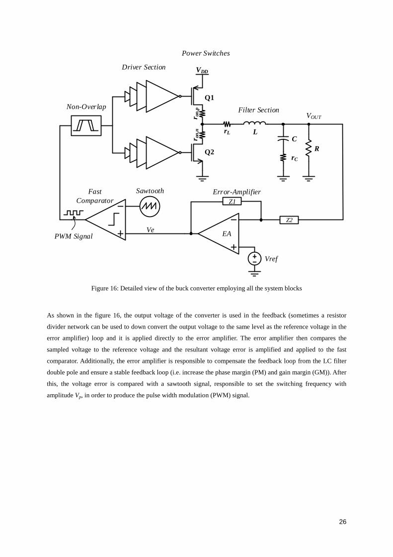
Figure 4: Buck converter waveforms for the (a) control, (b) inductor current, (c) inductor voltage and (d)
switching node, operating in the continuous conduction mode............................................................................. 10
Figure 5: Buck converter waveforms for the (a) control, (b) inductor current, (c) inductor voltage and (d)
switching node, operating at the discontinuous conduction mode .........................................................................11
Figure 6: Buck converter waveforms for the (a) control, (b) inductor current, (c) inductor voltage and (d)
switching node for the critical mode of operation................................................................................................. 12
Figure 7: (a) On-state of the synchronous buck converter. (b) Off-state of the synchronous buck converter. ...... 13
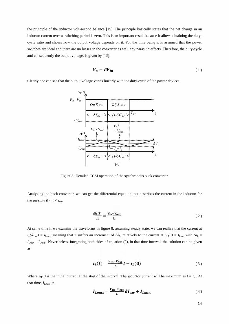
Figure 8: Detailed CCM operation of the synchronous buck converter. ............................................................... 14
Figure 9: Detailed DCM operation of the synchronous buck converter. ............................................................... 16
Figure 10: Equivalent circuit for the dead-time sub-interval conduction.............................................................. 16
Figure 11: A representative view of the buck converter output voltage ripple and inductor current ripple, for the
calculation of the output capacitor. ....................................................................................................................... 19
Figure 12: The equivalent buck converter circuit contemplating the conduction losses. ...................................... 20
Figure 21: Type II compensation circuit ............................................................................................................... 29
Figure 22: Type II asymptotic Bode plot............................................................................................................... 30
Figure 23: Type III compensation circuit. ............................................................................................................. 30
Figure 24: Type III asymptotic Bode plot ............................................................................................................. 31
Figure 25: Representation of the overall power stage block. ................................................................................ 33
xii
Figure 26: Determined values for the output filter used in the buck converter. .................................................... 34
Figure 27: Power switches showing the obtained channel width. ......................................................................... 35
Figure 28: Simulation showing the power switches on-resistance function of their width. .................................. 35
Figure 29: Power drivers consisting on a chain of inverters. ................................................................................ 37
Figure 30: The non-overlapping block consisting in a two NOR gates and two NOT gates. ................................ 38
Figure 31: The two non-overlapped signals to be applied at the input of the drivers............................................ 39
Figure 32: Test bench used to perform the PSS and PAC analysis in the buck converter. .................................... 41
Figure 33: Signals involved in the PWM wave generation. .................................................................................. 41
Figure 34: Open loop frequency response of the implemented buck converter. ................................................... 42
Figure 35: Open loop frequency response with no series resistance in the output inductor. ................................. 42
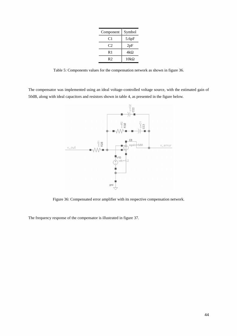
Figure 36: Compensated error amplifier with its respective compensation network. ........................................... 44
Figure 37: Frequency response of the designed compensator. .............................................................................. 45
Figure 38: Complete test bench used to perform the closed-loop feedback frequency response. ......................... 45
Figure 39: Closed Loop frequency response of the buck converter. ..................................................................... 46
Figure 40: Transient response comparison of the output voltage between the two crossover frequencies for a load
step of 50mA......................................................................................................................................................... 46
Figure 41: Comparison between the two closed loop frequency responses. ......................................................... 47
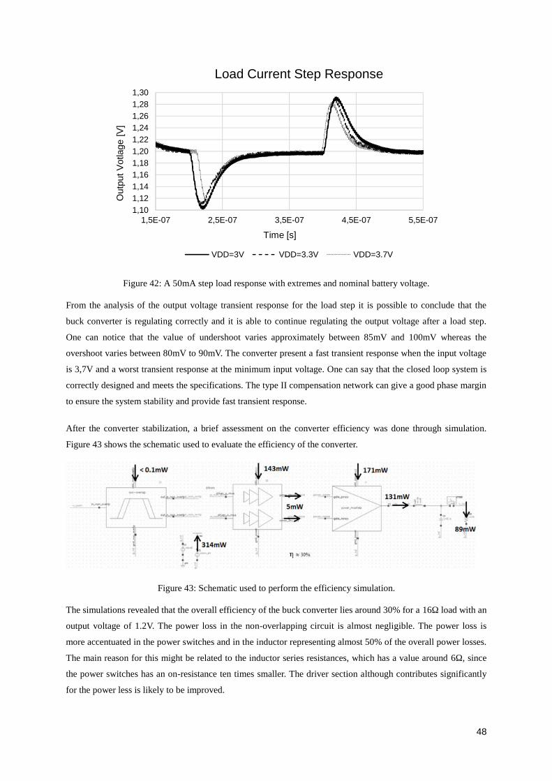
Figure 42: A 50mA step load response with extremes and nominal battery voltage. ............................................ 48
Figure 43: Schematic used to perform the efficiency simulation. ......................................................................... 48
Figure 74: Transient response of the buck converter for a load step of 50mA...................................................... 71
Figure 75: Transient response of the buck converter for line variations. .............................................................. 72
Figure 76: Transient response of the buck converter and BGVR for line variations............................................. 73
Figure 77: Transient response of the buck converter and BGVR without considering the line variation for the
bandgap voltage reference..................................................................................................................................... 73
Figure 78: Detailed view of the worst case transient response of the buck converter and BGVR without
considering the line variation for the bandgap voltage reference.......................................................................... 74
Figure 79: Detailed View of the floorplan of the die............................................................................................. 75
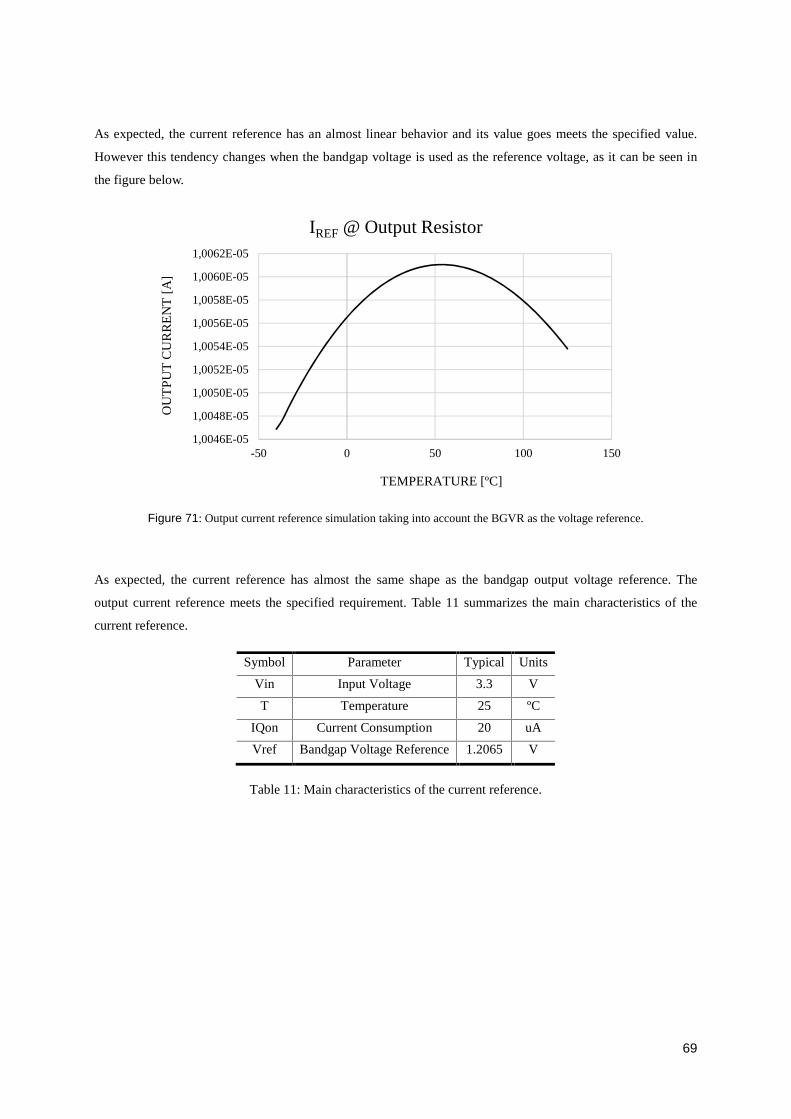
Figure 80: Detail of the single transistor that constitutes the power transistor ..................................................... 77
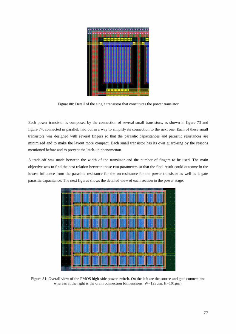
Figure 81: Overall view of the PMOS high-side power switch. On the left are the source and gate connections
whereas at the right is the drain connection (dimensions: W=123µm, H=101µm)............................................... 77
xiv
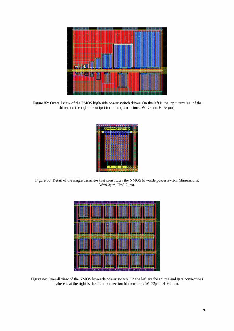
Figure 82: Overall view of the PMOS high-side power switch driver. On the left is the input terminal of the
driver, on the right the output terminal (dimensions: W=79µm, H=54µm). ......................................................... 78
Figure 83: Detail of the single transistor that constitutes the NMOS low-side power switch (dimensions:
Figure 84: Overall view of the NMOS low-side power switch. On the left are the source and gate connections
whereas at the right is the drain connection (dimensions: W=72µm, H=60µm)................................................... 78
Figure 85: Overall view of the NMOS low-side power switch driver. On the left is the input terminal of the
driver and at the right is the output terminal (dimensions: W=58µm, H=36µm).................................................. 79
Figure 86: Overall view of the power switches and their respective drivers......................................................... 80
Figure 87: Overall view of the bandgap voltage reference (dimensions: W=180µm, H=236µm). ....................... 80
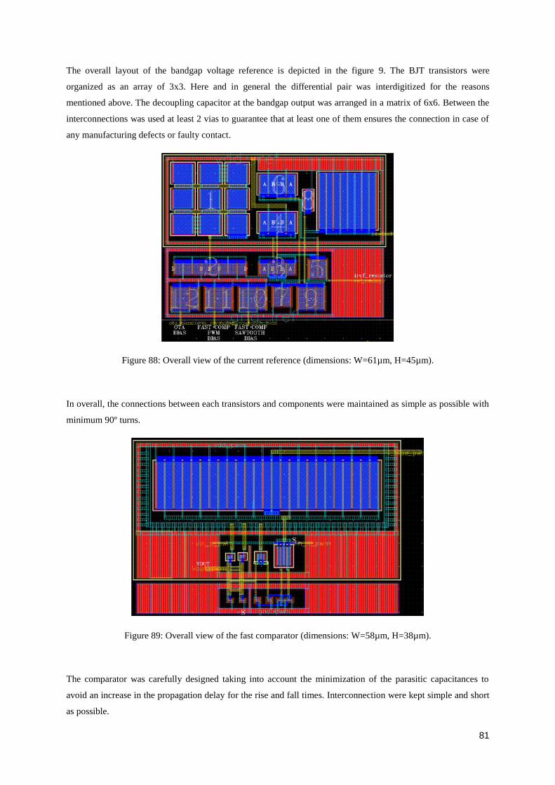
Figure 88: Overall view of the current reference (dimensions: W=61µm, H=45µm)........................................... 81
Figure 89: Overall view of the fast comparator (dimensions: W=58µm, H=38µm). ............................................ 81
Figure 90: Overall view of the MOSCAP (dimensions: W=755µm, H=781µm).................................................. 82
Figure 91: Overall view of the sawtooth generator (dimensions: W=40µm, H=35µm). ...................................... 82
Figure 92: Overall view of symmetrical operational transconductance amplifier................................................. 83
Figure 93: Overall view of the custom made metal track inductor (dimensions: W=335µm, H=335µm)............ 84
Figure 94: Overall view of the full chip (dimensions: W=1575µm, H=1575µm)................................................. 84
Figure 95: Post-layout test bench used to perform the post-layout simulation, including the pad connection as
well as the bonding wires...................................................................................................................................... 85
Figure 96: Post-layout buck converter operating at 75mA nominal output current with. ..................................... 86
Figure 97: Post-layout transient response of the buck converter for a load step of 50mA, from 75mA to 125mA.
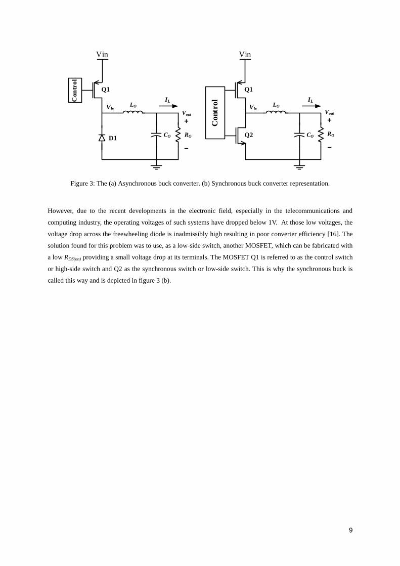
However, due to the recent developments in the electronic field, especially in the telecommunications and
computing industry, the operating voltages of such systems have dropped below 1V. At those low voltages, the
voltage drop across the freewheeling diode is inadmissibly high resulting in poor converter efficiency [16]. The
solution found for this problem was to use, as a low-side switch, another MOSFET, which can be fabricated with
a low RDS(on) providing a small voltage drop at its terminals. The MOSFET Q1 is referred to as the control switch
or high-side switch and Q2 as the synchronous switch or low-side switch. This is why the synchronous buck is
called this way and is depicted in figure 3 (b).
10
vL(t)
Vin - Vout
t
iL(t)
- Vout
t
IL=Io Δ IL
On State Off State
δTsw Tsw
δ(t)
t
Vin
t
vlx(t)
(a)
(b)
(c)
(d)
Figure 4: Buck converter waveforms for the (a) control, (b) inductor current, (c) inductor voltage and (d)
switching node, operating in the continuous conduction mode.
The buck converter can operate in two modes, those are, the continuous conduction mode (CCM) and the
discontinuous conduction mode (DCM), depending on the shape of the inductor current. In the CCM the inductor
current never goes to zero during the entire switching cycle as exemplified in figure 4, while the DCM is
characterized by the inductor current being zero during one portion of the switching cycle as depicted in figure 5.
It remains at zero for some time interval and starting from zero, increases until he reaches the peak value and
then returns to zero again, repeating each switching cycle.
11
vL(t)
Vin - Vout
t
iL(t)
- Vout
t
Δ IL
On State Off State
δTsw Tsw
δ(t)
t
vlx(t)
Vin
t
Vout
(a)
(b)
(c)
(d)
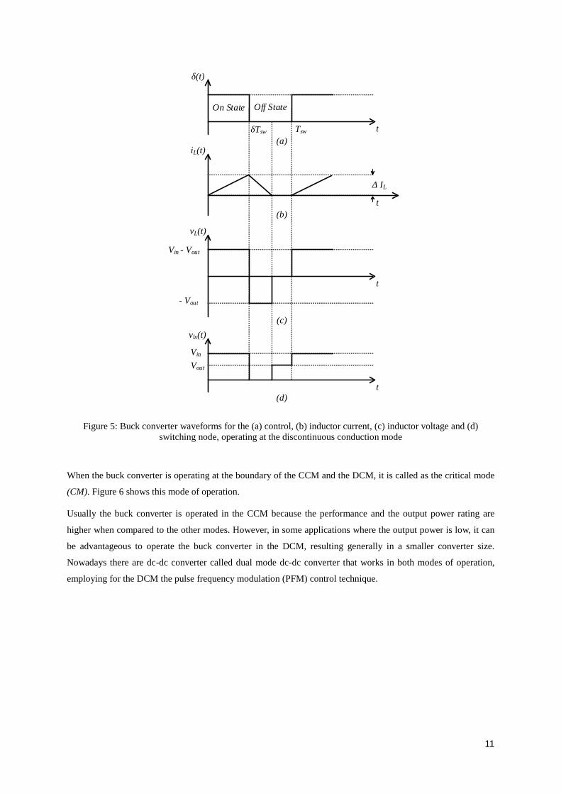
Figure 5: Buck converter waveforms for the (a) control, (b) inductor current, (c) inductor voltage and (d)switching node, operating at the discontinuous conduction mode
When the buck converter is operating at the boundary of the CCM and the DCM, it is called as the critical mode
(CM). Figure 6 shows this mode of operation.
Usually the buck converter is operated in the CCM because the performance and the output power rating are
higher when compared to the other modes. However, in some applications where the output power is low, it can
be advantageous to operate the buck converter in the DCM, resulting generally in a smaller converter size.
Nowadays there are dc-dc converter called dual mode dc-dc converter that works in both modes of operation,
employing for the DCM the pulse frequency modulation (PFM) control technique.
12
vL(t)
Vin - Vout
t
iL(t)
- Vout
t
IL=Io Δ IL
On State Off State
δTsw Tsw
δ(t)
t
Vin
t
vlx(t)
(a)
(b)
(c)
(d)
Figure 6: Buck converter waveforms for the (a) control, (b) inductor current, (c) inductor voltage and (d)switching node for the critical mode of operation.
In figure 7 is represented the two states that the circuit can take, the on-state and the off-state. The circuit is
composed by two MOSFETs, an inductor LO and capacitor CO. The inductor and capacitor will smooth the
current and voltage ripple, respectively, that goes to the load. The capacitor equivalent series resistance (ESR),
rC, and the inductor resistance, rL, are neglected for now. Finally, the load is represented by a resistor of value RO.
The operating principle analysis of the synchronous buck converter will be done assuming that the converter is
operating in the CCM. The buck converter is supplied by a DC voltage source of value Vin. This voltage is
chopped to the switching node Vlx with a square wave shape and then filtered by the second order LC low-pass
filter, converting it into dc output voltage.
13
SW1
LO
COSW2
IL
Vlx
Isw2
SW1
LO
COSW2
IL
Vlx
Isw1
Vin Vin
RO
Vout
RO
Vout
Figure 7: (a) On-state of the synchronous buck converter. (b) Off-state of the synchronous buck converter.
The SW1 and SW2 are turned on and off alternatively, complementarily to each other, with a certain switching
frequency fsw and duty cycle δ=ton/Tsw, where ton is the time interval when the switch SW1 is closed and Tsw is a
complete switching cycle. During the on-state, 0 < t < ton, as illustrated in figure 7 (a), the high-side switch SW1
is closed and the low-side switch SW2 is open. The power supply voltage is applied to the inductor and a voltage
is developed across it with a value of VL = Vin – Vout (assuming that there is no voltage drop across the high-side
switch). This potential difference, if positive, gives rise to a current in the inductor. The circuit waveforms are
shown in figure 7. As long as there will be a current flowing from the power supply to the load, the inductor will
store energy in its magnetic field, the capacitor will store energy in the electric field between its plates, and the
load will be fed.
Regarding the off-state, denoted as toff = (1- δ) Tsw, or ton < t < Tsw, the high-side switch SW1 will be open and
the low-side switch SW2 closed. The inductor will try to maintain his current flowing. During this period of time
the current decreases, because the voltage at his terminals is negative, of value VL = 0 – Vo < 0, (neglecting the
voltage drop across the low-side switch) since Vo > 0. The output voltage at the load terminals is always positive.
Please referrer to figure 8. The presence of the low-side switch allows an alternative path for the load current and
so for the inductor current, which cannot vary on a discontinuous way, flowing in the same direction. Without the
low-side switch SW2, the high-side switch SW1 could be destructed at the time of its cut-off.
2.2. Steady-State Analysis
The steady-state analysis is done for the operation in the CCM. A small reference to the DCM is made at the end
of this sub-chapter. For the steady-state analysis the principles of inductor volt-second balance and capacitor
charge balance are assumed. These are used so that the solution for the inductor currents and capacitor voltages
of the converter can be derived. Another useful approximation is the linear ripple approximation that facilitates
the steady state analysis. Steady-state means that the input voltage, output voltage and duty-cycle are not varying
with time. From this point onwards it will be possible to derive the filter elements of the converter.
As mentioned before, the buck converter changes the power supply voltage to a lower output voltage. This is
done by varying the duty-cycle of the converter. The derivation of the steady-state condition is made thanks to
14
the principle of the inductor volt-second balance [15]. The principle basically states that the net change in an
inductor current over a switching period is zero. This is an important result because it allows obtaining the duty-
cycle ratio and shows how the output voltage depends on it. For the time being it is assumed that the power
switches are ideal and there are no losses in the converter as well any parasitic effects. Therefore, the duty-cycle
and consequently the output voltage, is given by [15]:
= ( 1 )
Clearly one can see that the output voltage varies linearly with the duty-cycle of the power devices.
On State Off State
δTsw (1-δ)Tsw
vL(t)
Vin - Vout
t
δTsw (1-δ)Tsw
iL(t)
- Vout
t
ILmax
ILmin IL=Io
Vin - Vout
L- Vout
L
Δ IL
Tsw
(a)
(b)
Figure 8: Detailed CCM operation of the synchronous buck converter.
Analyzing the buck converter, we can get the differential equation that describes the current in the inductor for
the on-state 0 < t < ton:
( ) = ( 2 )
At same time if we examine the waveforms in figure 8, assuming steady state, we can realize that the current at
iL(δTsw) = iLmax, meaning that it suffers an increment of ΔiL, relatively to the current at iL (0) = ILmin with ΔiL =
ILmax – ILmin. Nevertheless, integrating both sides of equation (2), in that time interval, the solution can be given
as:
( ) = + ( ) ( 3 )
Where iL(0) is the initial current at the start of the interval. The inductor current will be maximum as t = ton. At
that time, ILmax is: = + ( 4 )
15
Now, considering the off-state, where ton < t < toff, when the high-side switch is off, the current in the inductor
completes its path through the low-side switch. Therefore, the equation that describes the current in the inductor
is: ( ) = − ( 5 )
Integrating both sides of equation (5), in that time interval, the solution is given as:
( ) = − + ( ) ( 6 )
Where iL(0) is the initial current at the start of the interval. The inductor current will be minimum at t = toff. At
that time, iLmin is:
= − ( − ) + ( 7 )
From (3) and (8) the incremental current ripple expression can be found to be:
= − = = ( − ) ( 8 )
Because the average current that flows into the inductor is the same as the one that goes to the load, we can
calculate the average current inductor as:
= = ( 9 )
The expression for the maximum and minimum currents that flows in the inductor can be now established. The
minimum current at the inductor, ILmin=iL (0), can be found by subtracting half of the total variation of the current
ΔIL to the average current of the inductor, which leads to:
= − = − ( − ) ( 10 )
And in the analogous way, ILmax=iL(δTsw), can be found by summing half of the total variation of the current ΔIL
to the average current of the inductor:
= + = + ( − ) ( 11 )
For an additional understanding refer again to figure 8. As mentioned before, the buck converter can operate in
the DCM under certain conditions. A brief description of the origins of this conduction mode is explained and
the duty-cycle conversion ratio is derived.
16
vL(t)
Vin - Vout
t
iL(t)
- Vout
t
Δ IL
(b)
(a)
δSW1Tsw
δSW2Tsw
δdtTsw
Vin - Vout
L
- Vout
L
ILmax
Figure 9: Detailed DCM operation of the synchronous buck converter.
While in the CCM the inductor current never goes to zero, the DCM is characterized by the inductor current
going to zero during one portion of the switching cycle. This affects greatly the properties of the converter, as for
an example, the conversion ratio becomes load dependent. Some issues regarding the converter dynamics are
also altered but it is a topic out of the scope of this work. For more information, refer to [15]. Typically this
mode occurs when we are in presence of large inductor current ripple and operating at light load, that is, the
converter is supplying a low output current. Since it is usually required that converter operate with their load
removed is normal to find them working under this condition. As illustrated in figure 9, there are now three sub-
intervals during the switching period Tsw. In the sub-interval δSW1Tsw, the high-side switch conducts, charging the
inductor and the capacitor while feeding the load at same time. The current increases from zero up to his
maximum value ILmax. In the next sub-interval δSW2Tsw, the low side-switch conducts. This time the
electromagnetic energy stored in the inductor is discharged into the output capacitor and the load, causing the
inductor current to decrease from its maximum value to zero. Finally, the remainder of the switching period,
δdtTsw, neither the high-side nor the low-side switches conduct, preventing IL to become negative as can be shown
in the figure below.
L
C R
VLIL
SW2
IO
Figure 10: Equivalent circuit for the dead-time sub-interval conduction.
After this sub-interval, every step will be repeated. With a few modifications, the same techniques and
approximations developed for the steady-state analysis of the CCM can be applied for this case [19], where the
new dc voltage transfer function is given by:
17
= = = ( 12 )
This introduces a new degree of freedom, yet with high inductor current ripple. In this relation it is possible to
verify that Vo/Vin<1.
2.2.1. Inductor Sizing
From (5) we can find the inductor value that guarantees a certain inductor current variation equals to ΔIL:
= = ( − ) ( 13 )
It can be proven that for a maximum ΔIL, the inductor has its maximum value for δ=1/2. From (13), the inductor
value is:
= = ( 14 )
This relation allows us to find the necessary inductor value to keep the maximum output current ripple bellow
the allowed maximum value for ΔiLmax.
However, if one needs to determine the minimum value of the inductor to ensure that the converter does not goes
to the DCM but stays in the limit of the CCM (critical mode), the ILmin ≥ 0, which means that:− ≥ ( 15 )
Therefore: − ( − ) ≥ ( 16 )
Leading to: ≥ ( − ) ( 17 )
This way one can ensure that the converter will work in the CCM if:≥ ( − ) ( 18 )
And in DCM if: ≤ ( − ) ( 19 )
18
2.2.2. Capacitor Sizing
As one can realize from figure 11, when the high-side switch is closed, that is, from 0 < t < ton, the charge
variation ΔQ supplied to the capacitor corresponds to the area of the triangle with base Tsw and height ΔiL/2:
∆ = = ( 20 )
Supposing that the output capacitor is assumed to be large enough and constant, ΔVo << Vo, as well as all the
ripple component in the inductor current flows through the capacitor, we get:
= → ∆ = ∆ ( 21 )
This means that the minimum filter capacitance required to reduce the ripple voltage bellow the specified value
is:
= ∆ ( ) = ∆ ( )( 22 )
This equation shows that the value of Co that guarantees a certain Vo /ΔVo is inversely proportional to the
switching frequency squared. Attending to [19]:
∆ = ( ) = ( − ) ( 23 )
Where,
= √ ( 24 )
It is another interesting way to explain how the voltage ripple can be minimized by selecting a corner frequency
of the low pass filter at the output of the buck converter such that fc << fsw. However one must be careful to
decide how big the output capacitor can be. Not only because it occupies a large area but, as it will be shown
ahead, because if the capacitor has a large ESR under some circumstances it can truly increase the output ripple
as it is represented in the figure below. The output voltage ripple here is represented as a slow moving sinusoidal
waveform, magnified for a better comprehension.
19
On State Off State
δTsw (1-δ)Tsw
vL(t)
Vin - Vout
t
δTsw (1-δ)Tsw
iL(t)
- Vout
t
ILmax
ILmin
IL=Io
ΔIL/2
Tsw
(a)
(b)
ΔQ
Tsw/2
δTsw (1-δ)Tsw
vC(t)
t
ΔVo
(c)
Vo
Figure 11: A representative view of the buck converter output voltage ripple and inductor current ripple, for thecalculation of the output capacitor.
2.2.3. Effects of Non-Idealities
Up until now we assumed that the buck converter was ideal and without losses. In fact, this is not true because
all these non-idealities influence the circuit behavior as well as all quantities that are processed in the converter,
namely the output voltage. The losses in the circuit are associated with the conduction losses and switching
losses as it will be seen more ahead. The conduction losses are related to the passive components, namely the
series resistance of the inductor, and with the on resistance of the high-side and low-side switches. Another
conduction loss, although not the most important, is associated with the ESR of the output capacitor. In figure 9
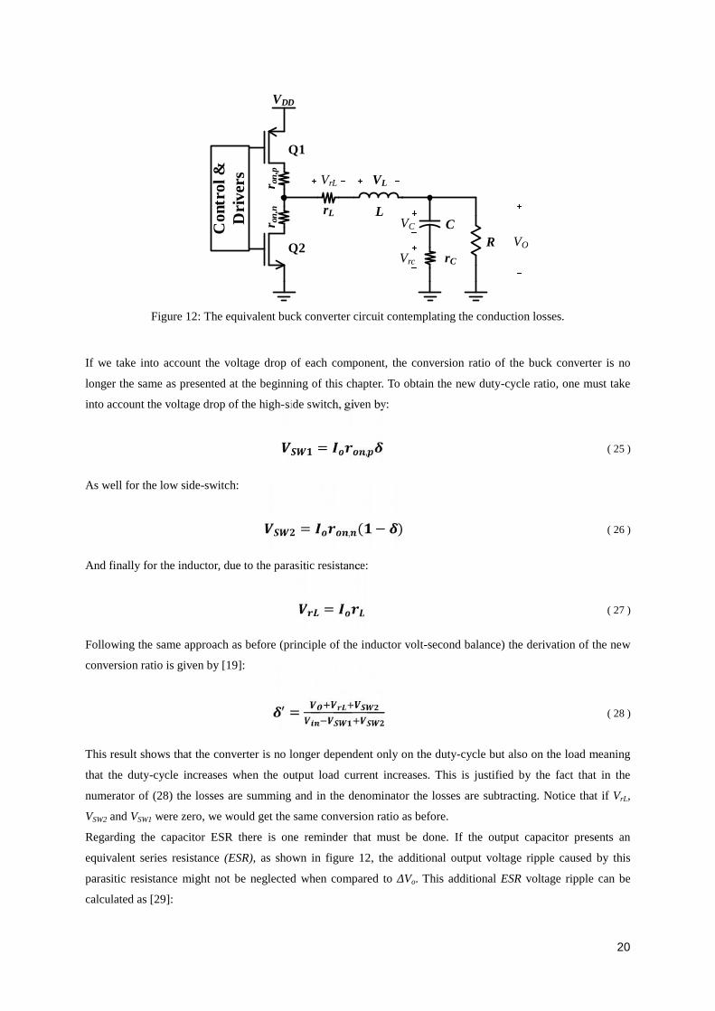
are presented the parasitic contribution for the considered conduction losses.
20
CR
rC
VC
Vrc
LrL
VL
VO
Q1
Q2
VDD
Con
trol
&D
rive
rs r on
,pr o
n,n
VrL
Figure 12: The equivalent buck converter circuit contemplating the conduction losses.
If we take into account the voltage drop of each component, the conversion ratio of the buck converter is no
longer the same as presented at the beginning of this chapter. To obtain the new duty-cycle ratio, one must take
into account the voltage drop of the high-side switch, given by:
= , ( 25 )
As well for the low side-switch:
= , ( − ) ( 26 )
And finally for the inductor, due to the parasitic resistance:
= ( 27 )
Following the same approach as before (principle of the inductor volt-second balance) the derivation of the new
conversion ratio is given by [19]:
= ( 28 )
This result shows that the converter is no longer dependent only on the duty-cycle but also on the load meaning
that the duty-cycle increases when the output load current increases. This is justified by the fact that in the
numerator of (28) the losses are summing and in the denominator the losses are subtracting. Notice that if VrL,
VSW2 and VSW1 were zero, we would get the same conversion ratio as before.
Regarding the capacitor ESR there is one reminder that must be done. If the output capacitor presents an
equivalent series resistance (ESR), as shown in figure 12, the additional output voltage ripple caused by this
parasitic resistance might not be neglected when compared to ΔVo. This additional ESR voltage ripple can be
calculated as [29]:
21
∆ = = ( − ) ( 29 )
The power dissipated on the ESR of the capacitor is proportional to the capacitor RMS current square. This
current shape is approximately equal to a triangular waveform of amplitude ΔiL/2, given by:
= √ ( 30 )
In order to minimize the power loss from the capacitor ESR, one must design a capacitor with the lowest ESR
value, capable of supporting ICRMS current, at the switching frequency. Another non-ideality related to the
capacitor is its equivalent series inductance (ESL), not represented in figure 12. The undesired effects caused by
the ESL are related to discontinuities in the output voltage at high frequency.
2.2.4. Efficiency and Power Loss Analysis
The efficiency and the power losses in a dc-dc converter are of great importance when designing a converter,
which means that a poor efficiency will be translated into excessive power dissipation and consequently a
considerable power waste. As mentioned before, the dc-dc converter losses are related to the static losses that are
related to the inductor, power switches, bonding-wire stray resistance and dynamic losses which basically
comprise the switching losses because of the charge and discharge of parasitic capacitances in the power devices.
This phenomenon occurs due to the hard switching event, where the current flows into the device, in its turn on
event, before the voltage across him collapses, as is roughly illustrated in the figure below. This type of losses is
proportional to the switching frequency.
VDSIDS
t
Figure 13: Mosfet hard-switching representation
The first source of losses to be analyzed is the conduction loss. The conduction losses basically occur when the
high-side or the low-side switches are conducting. They are calculated as the product between the square of the
transistor RMS current value that flows through him and its equivalent on-resistance. The expression that models
this resistance is obtained by the quadratic-model of the mosfet transistor considering that it is operating in the
triode region with a low VDS voltage [14]:
, = , ( 31 )
And
22
, = | | , ( 32 )
With βn=knW/L and βp=kpW/L respectably and kn,p=µn,pCox. However, it is important to tell that these equations
are more suitable to describe long channel MOSFETs. For short channel transistors, the models are far more
complex to make hand calculations and find only application in computational simulations. When the high-side
switch is conducting the associated conduction loss is given by [19]:
= , , ( 33 )
Where,
, = + ∆( 34 )
Or
, = ( 35 )
assuming the duty-cycle of the lossless converter and that the inductor current ripple is much smaller when
compared to the average inductor current, being this one equal to the output current in the steady-state operation.
Analogously, for the low-side switch, the conduction loss is:
= , , ( 36)
With
, = ( − ) + ∆( 37 )
Or
, = ( − ) ( 38 )
The other source of losses is the parasitic resistance of the inductor, ESR. This loss can be calculated as:
= ( 39 )
Where
23
= + ∆( 40 )
Finally, the last source of conduction loss is related to the body diodes of the switches. As it will be explained in
the next chapter, the high-side and low-side switches have an associated mechanism that prevents shoot-through
currents between the power supply and ground. This mechanism is known as dead-time generator which consists
of a non-overlap circuit that prevents both high-side and low-side switch from conducting simultaneously.
During this dead-time, both switches are supposed to be off, while the continuous inductor current flows through
the body diode of the low-side switch. When the body diode is conducting, its conduction loss can be calculated
as:
= ( 41 )
Where tdt is the total dead-time in one switching cycle. Please, do not confuse this dead-time with the dead-time
in DCM synchronous buck converters. If the dead-time generator is designed properly, the conduction loss from
the body-diode can be very small.
Now regarding the switching losses, these comprise the I-V overlap losses in the switch and the fCV2 losses,
which is directly proportional to the switching frequency. These losses are dominant at low load conditions and
at high frequencies. Moreover, these losses accounts with the turn-on and turn-off process. For sake of simplicity
the detailed mathematical treatment will not be presented. For more information refer to [21]. Assuming that the
turn-on and turn-off times are the same, the switching losses can be represented as:
= ( 42 )
Finally another switching loss is related to the gate drive. Essentially, the power dissipation in the gate drivers is
mostly due to the dynamic power used to charge and discharge the parasitic capacitor from the power devices.
This topic will not be discussed here. The global efficiency of the converter is found to be:
= = ∑ = ∑ ( 43 )
2.3. Buck Converter Feedback Control
A dc-dc converter must provide a regulated output voltage under several conditions such as load and input
voltage variations. Furthermore, the converter must ensure that the regulation is always achieved under process
variations, wide input voltage variations and different temperature range (PVT). However these are not the only
requisites when it comes to voltage regulation. There are some additional performance parameters that are
desired, such as, fast settling time, low overshoot and small ringing in the transient response.
24
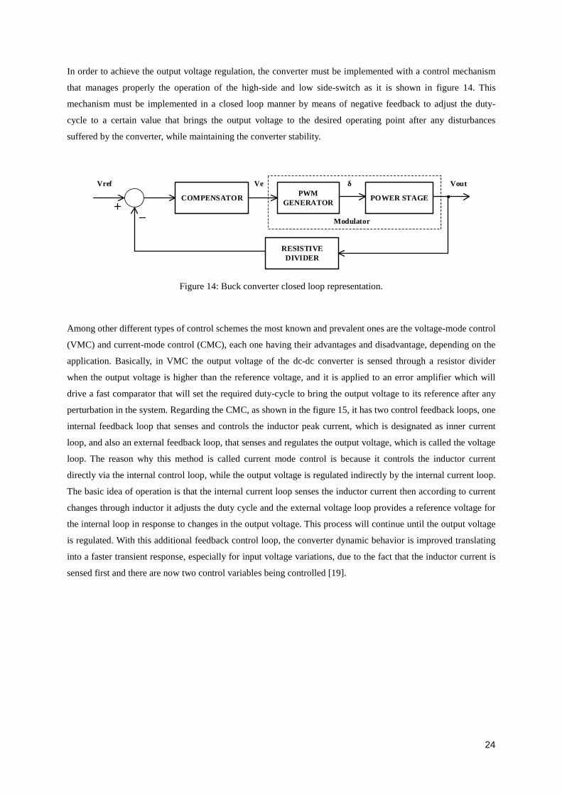
In order to achieve the output voltage regulation, the converter must be implemented with a control mechanism
that manages properly the operation of the high-side and low side-switch as it is shown in figure 14. This
mechanism must be implemented in a closed loop manner by means of negative feedback to adjust the duty-
cycle to a certain value that brings the output voltage to the desired operating point after any disturbances
suffered by the converter, while maintaining the converter stability.
Buck Converter Transient Response for a 50mA LoadStep
LOAD STEP IOUT VOUT
72
from 3.3V to 2.8V in 200ns was performed; afterwards an abruptly variation from 2.8V up to 4.2V and then from
4.2V to 2.8 was made in a 200ns interval. In the end a last line variation from 2.8V to 3.3 was accomplished in
200ns. The results are shown in the figure below.
Figure 75: Transient response of the buck converter for line variations.
Concerning the output voltage regulation, the worst case result was in the line variation from 2.8V up to 4.2V,
causing an overshoot of 185mV with 2.35µs of transient response followed by the variation from 3.3V to 4.2V
which presented an overshoot of 120mV with 1.35µs of transient response. In the other cases either the
overshoot or undershoot were below 90mV with a transient response below 1.35µs.
There is a one side note that worth some attention. The reference voltage from the BGVR is used in the feedback
control loop to set the desired output voltage reference and to generate the current reference. As we are varying
the input voltage of the converter and because this input voltage is supplying the BGVR there will be some error
introduced in the output voltage caused by the variation introduced by the BGVR due to line variation. Figure 76
shows the bandgap output voltage reference and the converter output voltage response to the line variation from
2.8V to 4.2V.
73
Figure 76: Transient response of the buck converter and BGVR for line variations.
This way, in order to evaluate the response of the system without the influence of the bandgap voltage reference
another line variation was performed for the worst case shown in figure 76, but now using a separately power
supply for the bandgap voltage reference. The results are shown below.
Figure 77: Transient response of the buck converter and BGVR without considering the line variation for thebandgap voltage reference.
74
In figure 78 it is possible to have a better look at the transient response.
Figure 78: Detailed view of the worst case transient response of the buck converter and BGVR withoutconsidering the line variation for the bandgap voltage reference.
As it is possible to realize, the system had a considerable improvement over the line transient response. The
controller is able to recover the output voltage in a very short time with a minimum overshoot and undershoot
effect. In worst case line variations, that was from 2.8V up to 4.2V the overshoot was below 50mV and the
converter was able to recover the output voltage within 450ns although with an output voltage error of 1.2%
when compared to its nominal operating output voltage.
75
5. Layout Implementation and Post-Layout Simulations
After the implementation of each block in the schematic view, this chapter will give emphasis to the layout
implementation and the top-level post-layout simulations. The layout of this system was implemented using the
standard CMOS UMC 130nm MM/RF technology. In first place, a careful planning of the floorplan was done, as
presented below, showing the location of the bond-pads and each functional cell. This floorplan serves as a guide
during the layout although it can be changed and revised accordingly whenever necessary.
VDD CONTROLEXT. R.VDDPOWER
VD
D P
OW
ER
GN
D P
OW
ER
GND POWER
GND CONTROL
GN
D C
AP
AC
ITO
RO
UT
PU
T
OUTPUTCAPACITOR
OUTPUTINDUCTOR
POWER STAGECONTROL
1570
µm
1570µm
Figure 79: Detailed View of the floorplan of the die.
In a dc-dc converter, the layout is of highest importance, especially when operating at very-high frequency
where the performance of the system can become degraded if a careless layout is done. Thus, some relevant
implementation details that can affect the functioning and performance of the converter must be taken into
76
account. Therefore some of the relevant layout practices used in this work are described, such as substrate noise
effects, power transistors layout, number of metal layers and their routing as well as the importance of keeping
the size of each cell as small as possible.
5.1. Substrate Noise Effects
One of the most important issues in the layout of this work is related to substrate noise since the dc-dc converter
has different blocks that generates electrical disturbing signals, like power switches operating at very high
frequency and their respective drivers. Hence the substrate is prone to noise injected by the switching behavior
of the power stage that can influence the performance of other analog blocks, as they share the same substrate.
These disturbances should be minimized as much as possible as it will be explained below. This source of noise
is the capacitive coupling between the interconnections and the substrate and junction capacitances between the
n-wells and the substrate.
5.2. Power Supply and Ground Planning
Because there are no perfect ground and power nodes inside the chip, the bonding wires inductance creates
crosstalk between different parts of the circuit and system. To minimize this effect the power supply was
separated into two rails, one for the power block and another for the control block. For the same reason different
ground rails were also used. Therefore each section sees its own noise, being the control noise very small when
compared to the one generated by the power stage. This solution implied the use of several pads, which leads to
an increase in the occupied area.
5.3. Power Transistors and Drivers Considerations
A special attention was given to the power transistor and their respective drivers from the perspective of isolating
each one with a guard-ring (depicted in the figure 73) as they are the major source of noise and susceptible to
inject majorities carrier’s (electrons and holes) into the substrate due to the switching activity.
As for an example, during the converter operation, the switching node Vlx, and therefore the VDS of the low-side
switch, can go below the substrate potential leading to some charge injection in the substrate. The same thing can
happen if that same switching node (or any other) voltage goes above the VDD voltage. Those voltage spikes can
be sufficient to directly bias the parasitic junctions between the drain/source and substrate/n-well.
The reason could be exactly because of the above mentioned switching behavior of the power transistors but also
because resistive power and ground path from the power PADs to the substrate and N-WELL. So additional
routing of the power and ground paths must be designed carefully.
Another issue created by the bonding wires is the generation of large di/dt values which gives rise to power
supply bouncing when large currents flows through, which can be dangerous if the voltages limits are exceeded.
77
Figure 80: Detail of the single transistor that constitutes the power transistor
Each power transistor is composed by the connection of several small transistors, as shown in figure 73 and
figure 74, connected in parallel, laid out in a way to simplify its connection to the next one. Each of these small
transistors was designed with several fingers so that the parasitic capacitances and parasitic resistances are
minimized and to make the layout more compact. Each small transistor has its own guard-ring by the reasons
mentioned before and to prevent the latch-up phenomenon.
A trade-off was made between the width of the transistor and the number of fingers to be used. The main
objective was to find the best relation between those two parameters so that the final result could outcome in the
lowest influence from the parasitic resistance for the on-resistance for the power transistor as well as it gate
parasitic capacitance. The next figures shows the detailed view of each section in the power stage.
Figure 81: Overall view of the PMOS high-side power switch. On the left are the source and gate connectionswhereas at the right is the drain connection (dimensions: W=123µm, H=101µm).
78
Figure 82: Overall view of the PMOS high-side power switch driver. On the left is the input terminal of thedriver, on the right the output terminal (dimensions: W=79µm, H=54µm).
Figure 83: Detail of the single transistor that constitutes the NMOS low-side power switch (dimensions:W=9.3µm, H=8.7µm).
Figure 84: Overall view of the NMOS low-side power switch. On the left are the source and gate connectionswhereas at the right is the drain connection (dimensions: W=72µm, H=60µm).
79
Figure 85: Overall view of the NMOS low-side power switch driver. On the left is the input terminal of thedriver and at the right is the output terminal (dimensions: W=58µm, H=36µm).
In the design of the power drivers, the gate of each transistor was designed with poly and metal 1 to reduce as
much as possible the high gate resistance to avoid large distributed RC delay effect.
5.4. Layout Implementation of Each BlockSome of the most known layout techniques [18] were taken into account. Generally, it was given attention to
symmetry for better matching, multi-finger transistors to reduce parasitic capacitances; current mirrors were
interdigitized as well as differential pairs instead of using common centroid technique, to avoid additional
parasitic capacitances. Whenever possible the source terminals of a multi-finger transistor were realized by the
outer fingers and the drain terminals by the inner fingers since those are critical nodes especially for the
differential pairs as they influence the speed of the amplifier. Overlapping between signals lines was avoided
unless impossible, and interconnections were kept as short as possible. In the next figures each block that
composes the dc-dc buck converter is shown. Interconnections with poly were avoided because of their parasitic
resistance and high parasitic capacitance to substrate. Routing over the gates of critical transistor and their
respective active areas is avoided. It was always given preference to short metal connection between each block
and prevent very long metal lines to keep the voltage drop very low. When that was not possible, the ones that
were longer were made wide enough and stacked with one or more metals through vias to at least neglect their
resistive effect.
80
Figure 86: Overall view of the power switches and their respective drivers
The overall layout of the power block is depicted in the figure 8. Metals were connected by as many vias as
possible to reduce the resistance and avoid current crowding in vias. For the power supply path, metal 1 up to
metal 5 were used to minimize the parasitic resistance and allow high current densities. The maximum width
used was 10µm to avoid slotting. The 90º corners are avoided in the drain output node since it is a critical node
where will be processed high current densities. Here it was used 8 metal layers, starting in metal 2 and gradually
increasing those metals up to metal 8. Several vias was used to interconnect the metal layers between them and
therefore reduce the parasitic resistance. Narrower paths were avoided in the path of high currents to avoid high
current densities or current crowding so as to avoid electromigration. The power transistors were arranged in a
way to get an array not too different from a square-like shape.
Figure 87: Overall view of the bandgap voltage reference (dimensions: W=180µm, H=236µm).
81
The overall layout of the bandgap voltage reference is depicted in the figure 9. The BJT transistors were
organized as an array of 3x3. Here and in general the differential pair was interdigitized for the reasons
mentioned above. The decoupling capacitor at the bandgap output was arranged in a matrix of 6x6. Between the
interconnections was used at least 2 vias to guarantee that at least one of them ensures the connection in case of
any manufacturing defects or faulty contact.
Figure 88: Overall view of the current reference (dimensions: W=61µm, H=45µm).
In overall, the connections between each transistors and components were maintained as simple as possible with
minimum 90º turns.
Figure 89: Overall view of the fast comparator (dimensions: W=58µm, H=38µm).
The comparator was carefully designed taking into account the minimization of the parasitic capacitances to
avoid an increase in the propagation delay for the rise and fall times. Interconnection were kept simple and short
as possible.
82
Figure 90: Overall view of the MOSCAP (dimensions: W=755µm, H=781µm).
Figure 91: Overall view of the sawtooth generator (dimensions: W=40µm, H=35µm).
An additional guard-ring around the capacitor was implemented.
83
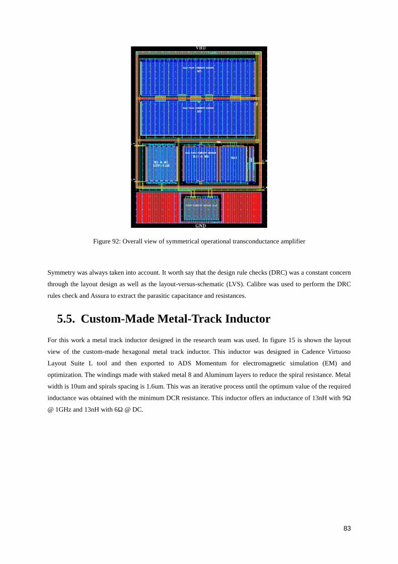
Figure 92: Overall view of symmetrical operational transconductance amplifier
Symmetry was always taken into account. It worth say that the design rule checks (DRC) was a constant concern
through the layout design as well as the layout-versus-schematic (LVS). Calibre was used to perform the DRC
rules check and Assura to extract the parasitic capacitance and resistances.
5.5. Custom-Made Metal-Track InductorFor this work a metal track inductor designed in the research team was used. In figure 15 is shown the layout
view of the custom-made hexagonal metal track inductor. This inductor was designed in Cadence Virtuoso
Layout Suite L tool and then exported to ADS Momentum for electromagnetic simulation (EM) and
optimization. The windings made with staked metal 8 and Aluminum layers to reduce the spiral resistance. Metal
width is 10um and spirals spacing is 1.6um. This was an iterative process until the optimum value of the required
inductance was obtained with the minimum DCR resistance. This inductor offers an inductance of 13nH with 9Ω
@ 1GHz and 13nH with 6Ω @ DC.
84
Figure 93: Overall view of the custom made metal track inductor (dimensions: W=335µm, H=335µm).
The DC resistance of 6Ω obtained with EM simulations is too pessimistic because the metals resistivity typical
values provided by the manufacturer are valid for a 1.5um width metal stripe. Also by comparing with similar
inductors provided by the foundry design kit, it is possible to see that they present around 6Ω resistance with
only metal 8 windings.
Figure 94: Overall view of the full chip (dimensions: W=1575µm, H=1575µm).
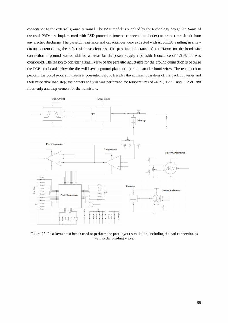
5.6. Post-Layout SimulationsIn this section the post-layout simulations of the overall dc-dc buck converter is presented. For the post-layout
simulations the bonding wires and PAD connections were considered. It contains an inductances and a
85
capacitance to the external ground terminal. The PAD model is supplied by the technology design kit. Some of
the used PADs are implemented with ESD protection (mosfet connected as diodes) to protect the circuit from
any electric discharge. The parasitic resistance and capacitances were extracted with ASSURA resulting in a new
circuit contemplating the effect of those elements. The parasitic inductance of 1.1nH/mm for the bond-wire
connection to ground was considered whereas for the power supply a parasitic inductance of 1.6nH/mm was
considered. The reason to consider a small value of the parasitic inductance for the ground connection is because
the PCB test-board below the die will have a ground plane that permits smaller bond-wires. The test bench to
perform the post-layout simulation is presented below. Besides the nominal operation of the buck converter and
their respective load step, the corners analysis was performed for temperatures of -40ºC, +25ºC and +125ºC and
ff, ss, snfp and fnsp corners for the transistors.
Figure 95: Post-layout test bench used to perform the post-layout simulation, including the pad connection aswell as the bonding wires.
86
5.6.1. Nominal Conditions of Operation
Figure 96: Post-layout buck converter operating at 75mA nominal output current with.
In the nominal operation of the buck converter with the RC extracted performed, one can notice that there is a
larger voltage ripple when compared to the results before layout. Here a ripple of 85mV is visible, which
corresponds to a 6% of the output voltage. This output voltage ripple can be related to the output capacitor that
was implemented through an array of mosfets connected as a capacitor (MOSCAP). As this type of capacitances
uses the gate of the mosfet, which is made of polysilicon, there might be some influences from the polysilicon
gate resistance along with the extracted R parameter (overall ESR) that contributes to output ripple. From the
point of view of the inductor current, it’s possible to appreciate a ripple around 110mA centered in the nominal
output current of 75mA. As long as the minimum inductor current is positive, the converter will be operating in
the CCM. For the nominal condition of operation of 3.3V of input voltage and 1.2V of output voltage into a load


![Homepage - MAC 5950 Sistemas Humano Computacionais ...sistemas-humano-computacionais.wdfiles.com/local... · Author: localadmin [ GROUPER ] Created Date: 8/15/2002 5:22:10 PM](https://static.documents.pub/doc/80x56/5f9765286be8da19ff51ed15/homepage-mac-5950-sistemas-humano-computacionais-sistemas-humano-author-localadmin.jpg)


