FULLY MONOLITHIC CMOS NICKEL MICROMECHANICAL RESONATOR OSCILLATOR FOR WIRELESS COMMUNICATIONS by Wen-Lung Huang A dissertation submitted in partial fulfillment of the requirements for the degree of Doctor of Philosophy (Electrical Engineering) in The University of Michigan 2008 Doctoral Committee: Professor Clark T.-C. Nguyen, Co-Chair Assistant Professor Michel M. Maharbiz, Co-Chair Professor Noel C. Perkins Assistant Professor Jamie D. Phillips
Transcript
FULLY MONOLITHIC CMOS NICKEL MICROMECHANICAL RESONATOR OSCILLATOR FOR WIRELESS COMMUNICATIONS
by
Wen-Lung Huang
A dissertation submitted in partial fulfillment of the requirements for the degree of
Doctor of Philosophy (Electrical Engineering)
in The University of Michigan 2008
Doctoral Committee:
Professor Clark T.-C. Nguyen, Co-Chair Assistant Professor Michel M. Maharbiz, Co-Chair Professor Noel C. Perkins Assistant Professor Jamie D. Phillips
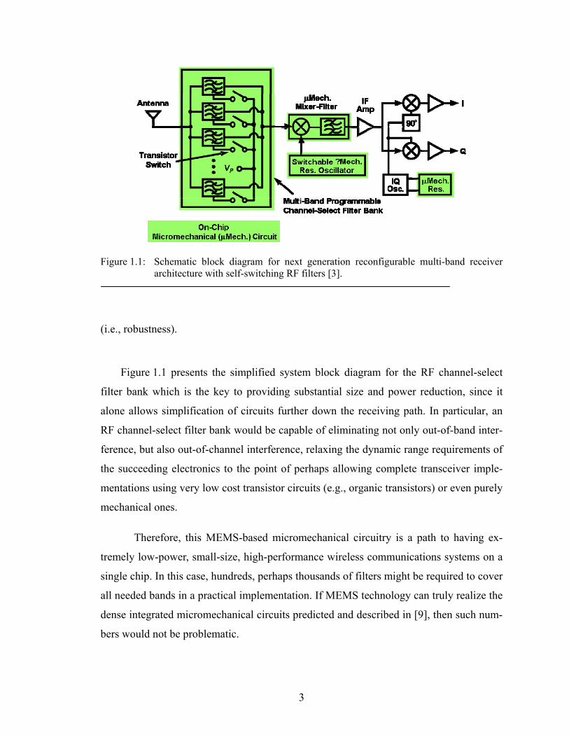
Figure 1.1: Schematic block diagram for next generation reconfigurable multi-band receiver architecture with self-switching RF filters [3]. ............................. 3
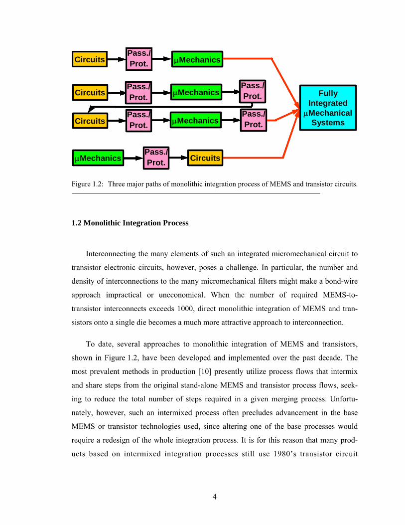
Figure 1.2: Three major paths of monolithic integration process of MEMS and transistor circuits......................................................................................... 4
Figure 1.3: Photo of the Analog Devices ADXL50 shows a micro-machined stand-alone accelerometer along with the appropriate signal conditioning circuitry and the zoomed SEM’s of a fabricated MEMS accelerometer..... 5
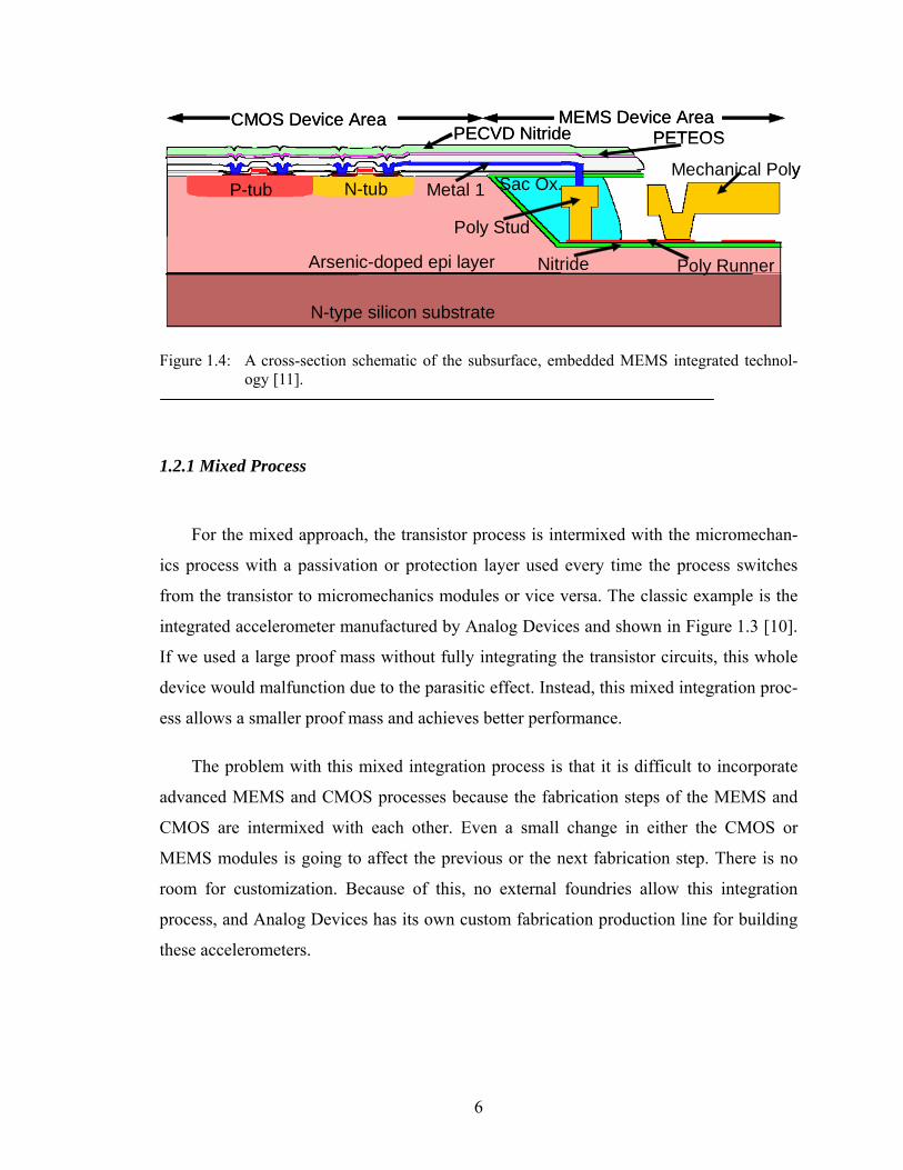
Figure 1.4: A cross-section schematic of the subsurface, embedded MEMS integrated technology [11]. .......................................................................................... 6
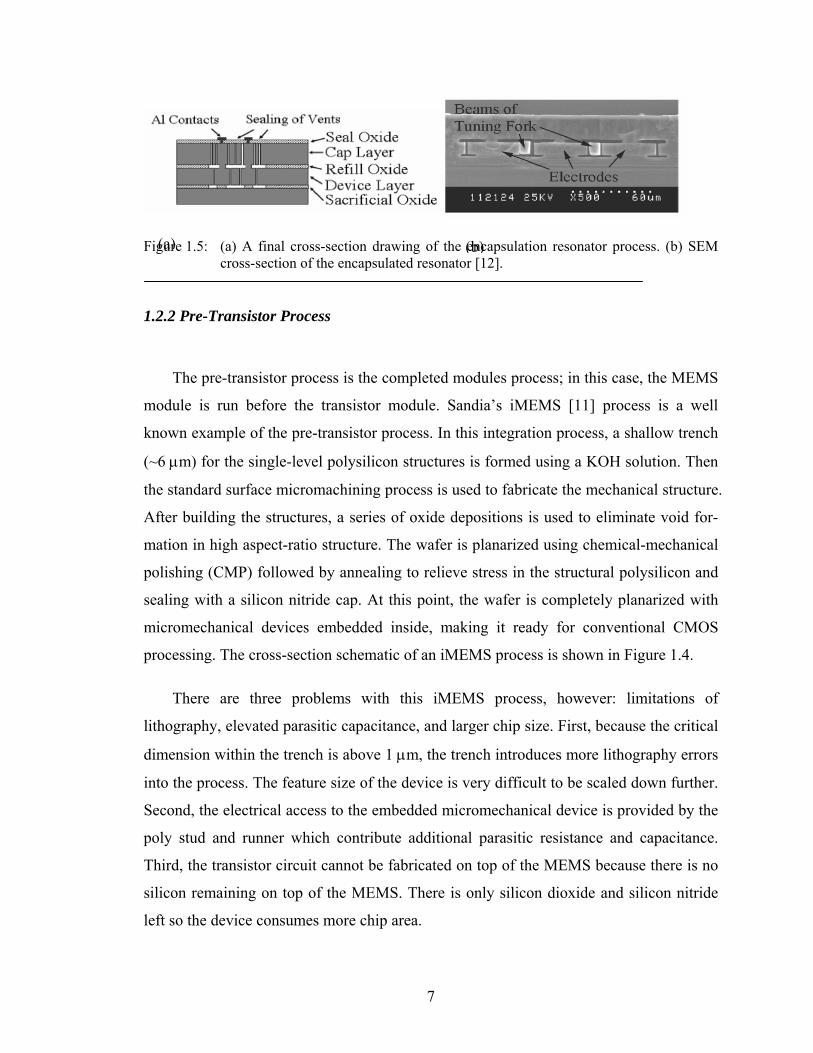
Figure 1.5: (a) A final cross-section drawing of the encapsulation resonator process. (b) SEM cross-section of the encapsulated resonator [12]. .............................. 7
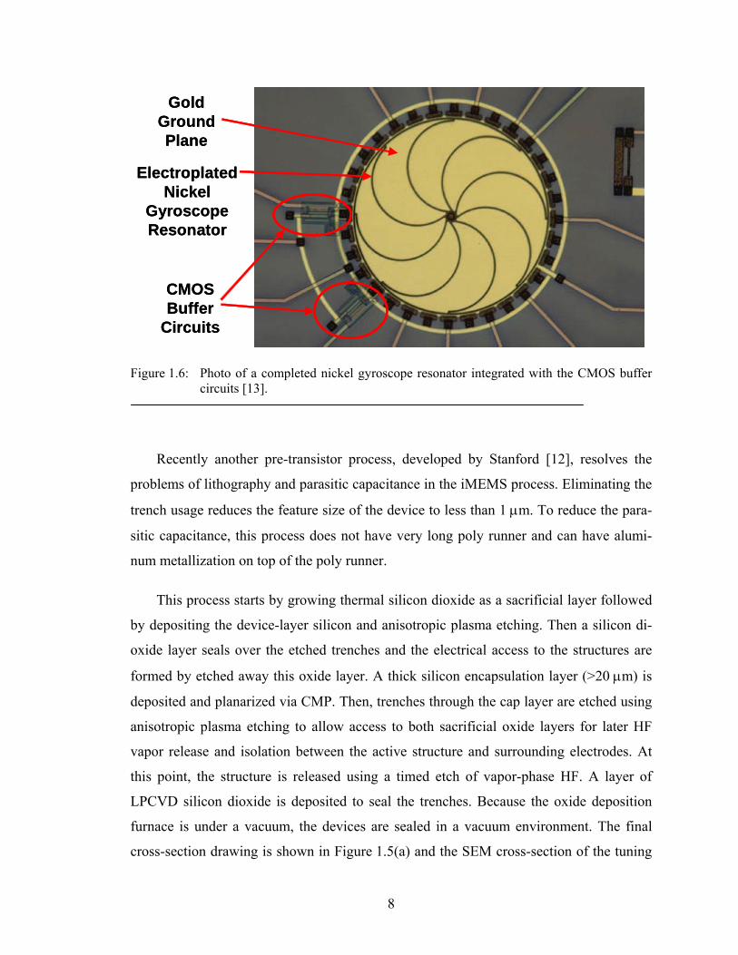
Figure 1.6: Photo of a completed nickel gyroscope resonator integrated with the CMOS buffer circuits [13]. ......................................................................... 8
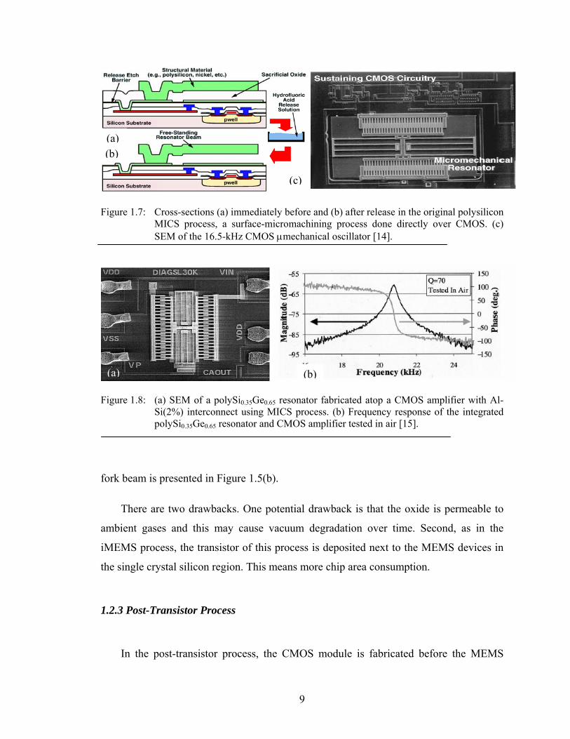
Figure 1.7: Cross-sections (a) immediately before and (b) after release in the original polysilicon MICS process, a surface-micromachining process done directly over CMOS. (c) SEM of the 16.5-kHz CMOS μmechanical oscillator [14]. ............................................................................................. 9
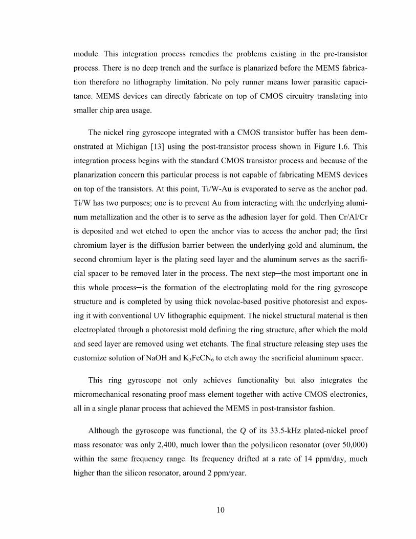
Figure 1.8: (a) SEM of a polySi0.35Ge0.65 resonator fabricated atop a CMOS amplifier with Al-Si(2%) interconnect using MICS process. (b) Frequency response of the integrated polySi0.35Ge0.65 resonator and CMOS amplifier tested in air [15]......................................................................................................... 9
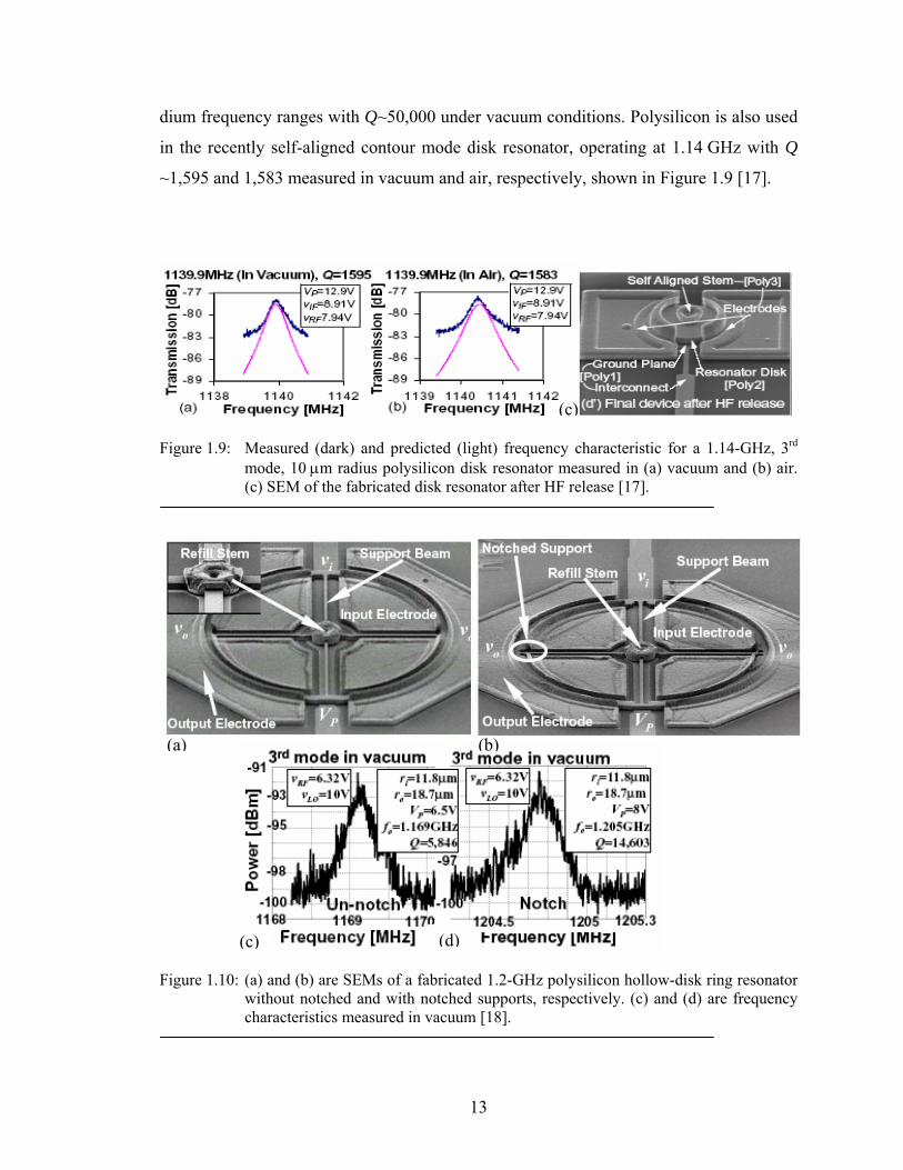
Figure 1.9: Measured (dark) and predicted (light) frequency characteristic for a 1.14-GHz, 3rd mode, 10 μm radius polysilicon disk resonator measured in (a) vacuum and (b) air. (c) SEM of the fabricated disk resonator after HF release [17]................................................................................................ 13
Figure 1.10: (a) and (b) are SEMs of a fabricated 1.2-GHz polysilicon hollow-disk ring resonator without notched and with notched supports, respectively. (c) and (d) are frequency characteristics measured in vacuum [18]. .................... 13
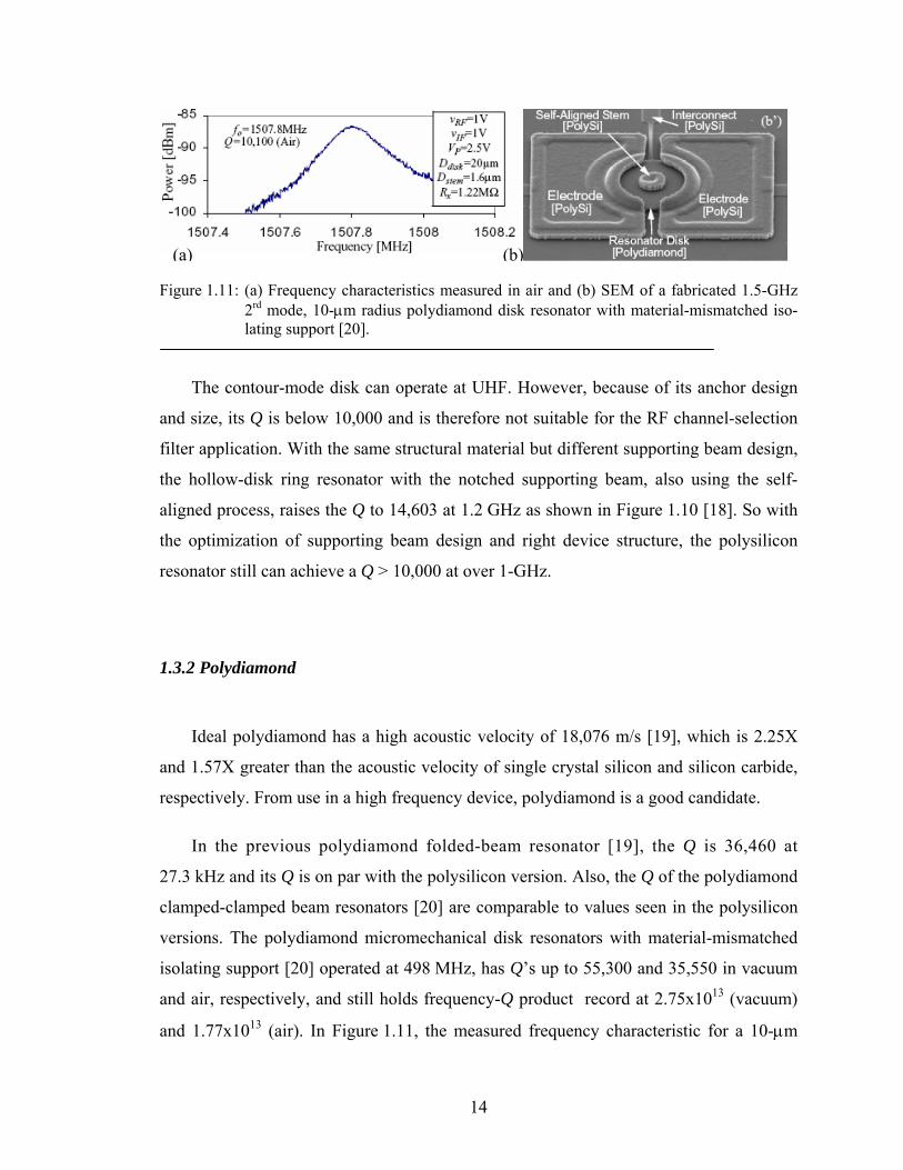
Figure 1.11: (a) Frequency characteristics measured in air and (b) SEM of a fabricated 1.5-GHz 2rd mode, 10-μm radius polydiamond disk resonator with
ix
material-mismatched isolating support [20]. ............................................ 14
Figure 1.12: (a) Poly-SiC Lamé-mode resonator with 195nm FIB-cut transducer gap. (b) The measured frequency characteristic using the fully differential electrode configuration [22]...................................................................... 15
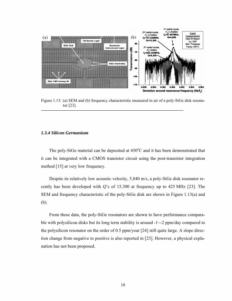
Figure 1.13: (a) SEM and (b) frequency characteristic measured in air of a poly-SiGe disk resonator [23]. ................................................................................... 16
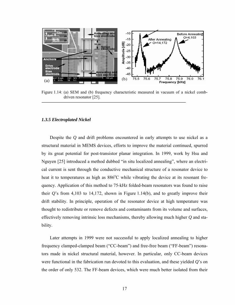
Figure 1.14: (a) SEM and (b) frequency characteristic measured in vacuum of a nickel comb-driven resonator [25]. ..................................................................... 17
Figure 1.15: General series-resonant oscillator circuit topology................................... 20
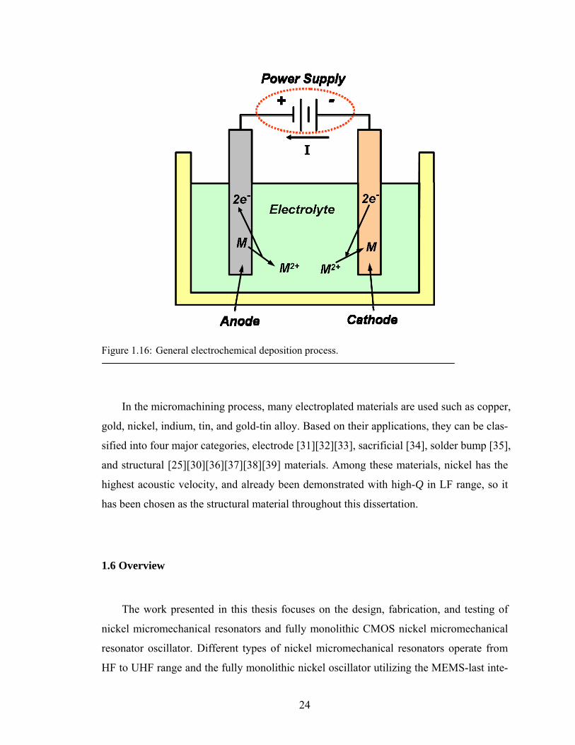
Figure 1.16: General electrochemical deposition process............................................. 24
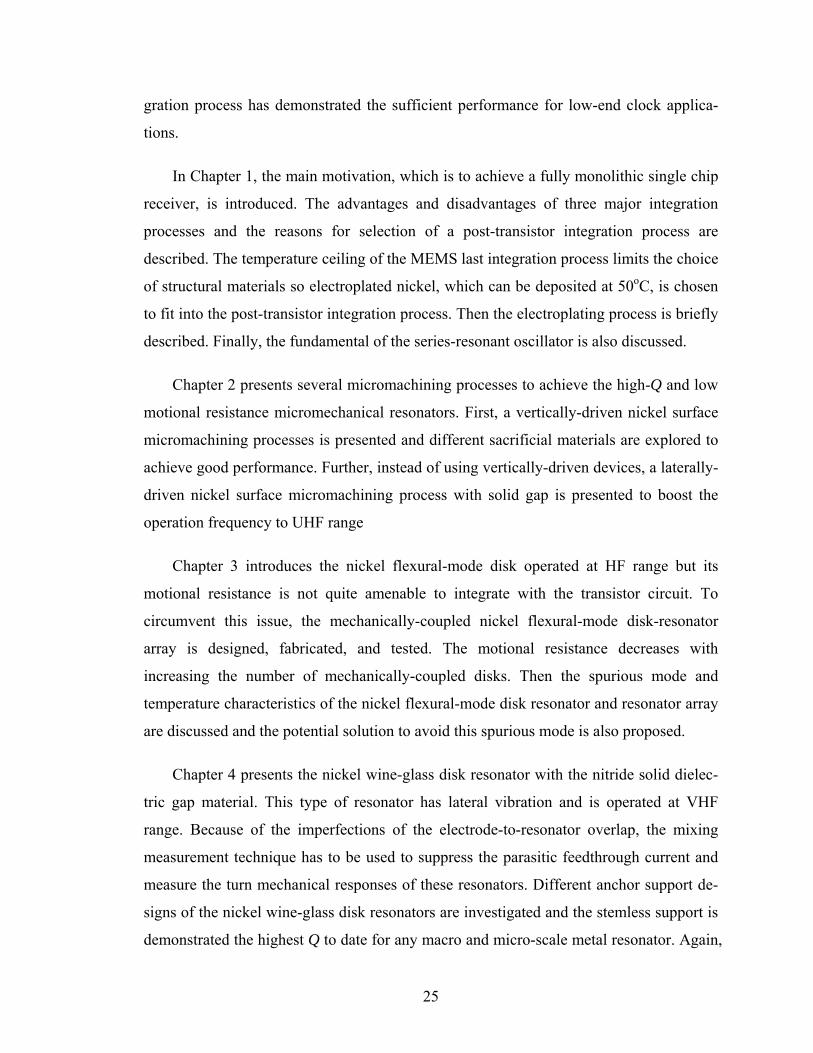
Figure 2.1: Cross sectional fabrication process flow for vertically-driven nickel flexural mode disk resonators with aluminum as sacrificial layer............ 29
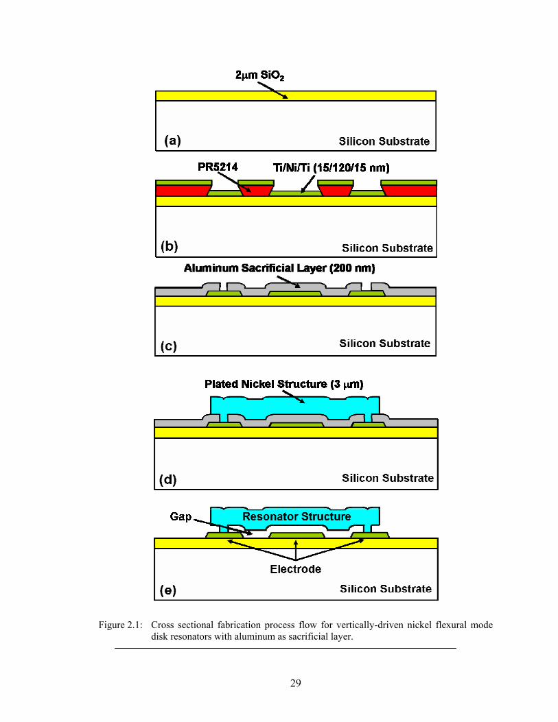
Figure 2.2: Step coverage on trenches in typical physical vapor deposition techniques is illustrated............................................................................................... 30
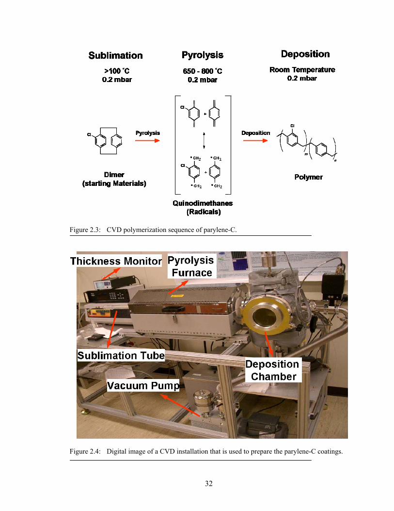
Figure 2.3: CVD polymerization sequence of parylene-C. ......................................... 32
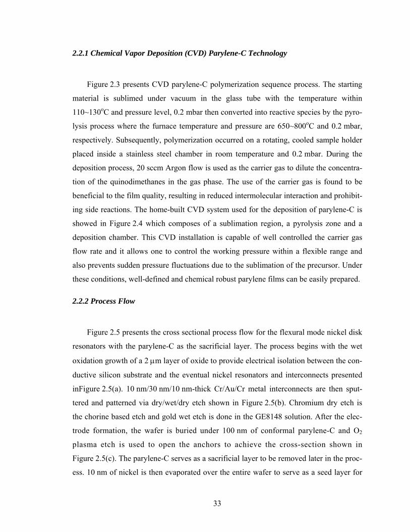
Figure 2.4: Digital image of a CVD installation that is used to prepare the parylene-C coatings. .................................................................................................... 32
Figure 2.5: Cross sectional fabrication process flow for vertically-driven nickel flexural mode disk resonators with parylene-C as sacrificial layer. ......... 34
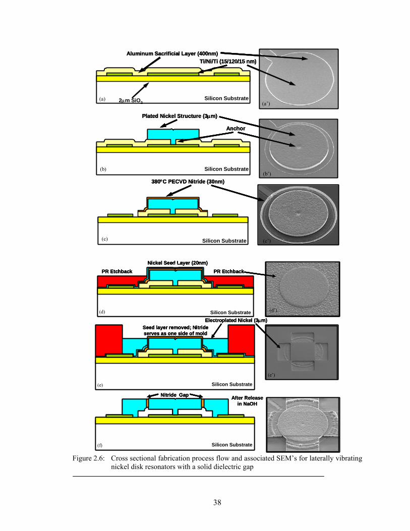
Figure 2.6: Cross sectional fabrication process flow and associated SEM’s for laterally vibrating nickel disk resonators with a solid dielectric gap...................... 38
Figure 2.7: (a) Globe-view and (b) gap-zoomed SEM’s of a fabricated nickel disk resonator supported by a stem anchored at its center................................ 39
Figure 3.1: (a) Perspective-view schematic of a flexural mode disk micromechanical resonator in a two-port bias configuration and (b) its top-view illustration with polar coordination............................................................................. 42
Figure 3.2: Mode shape of a flexural-mode side-supported disk resonator simulated via ANSYS................................................................................................ 43
Figure 3.3: LCR equivalent circuit modal of the flexural-mode disk resonator of Figure 3.1. ................................................................................................. 46
Figure 3.4: Simplified LCR equivalent circuit model presenting the real measurement setup of the flexural mode disk resonator. ................................................ 47
x
Figure 3.5: Final cross section of the nickel surface micromachining process for a flexural-mode disk micromechanical resonator. The completed process flows are described in section 2.1.1 and 2.2.2. ......................................... 48
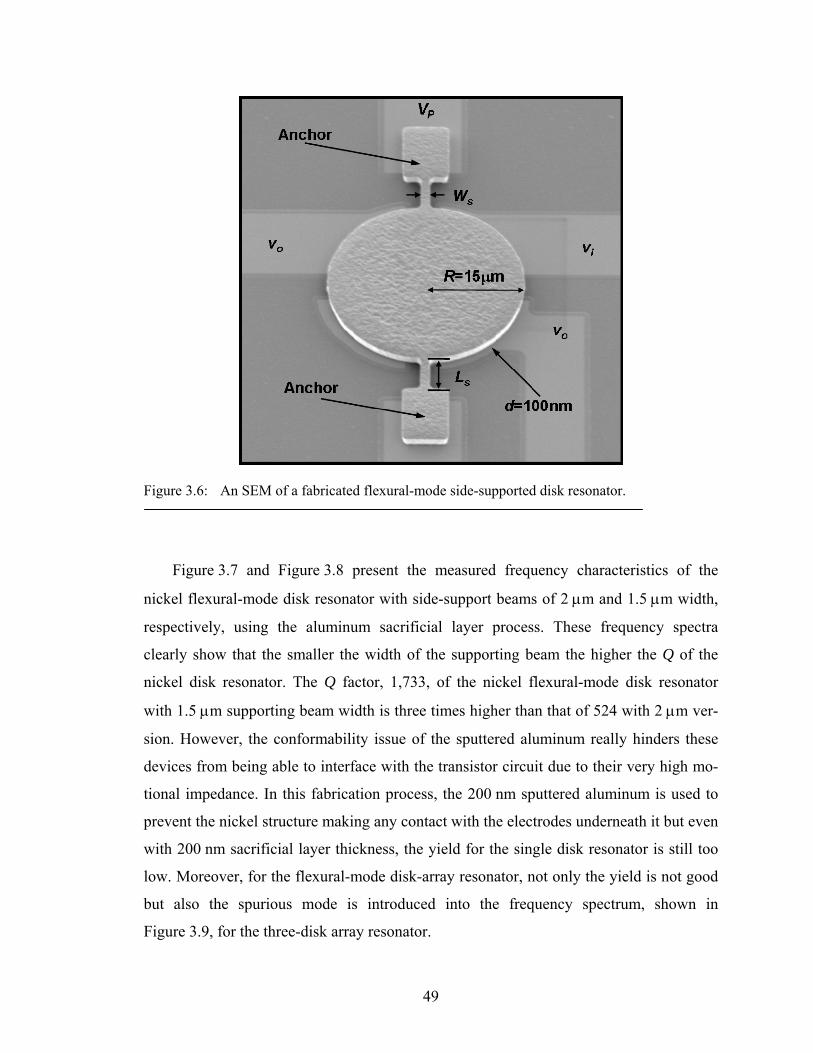
Figure 3.6: An SEM of a fabricated flexural-mode side-supported disk resonator..... 49
Figure 3.7: Measured open-loop frequency spectrum for the nickel flexural-mode disk resonator with 2 μm supporting beam width fabricated via the use of the aluminum as the sacrificial layer. ............................................................. 50
Figure 3.8: Measured open-loop frequency spectrum for the nickel flexural-mode disk resonator with 1.5 μm supporting beam width fabricated by using the aluminum as the sacrificial layer. ............................................................. 50
Figure 3.9: Measured open-loop frequency spectrum shown the spurious mode for the three nickel mechanically-coupled flexural-mode disks resonator array with 1.5 μm supporting beam width fabricated by using the aluminum as the sacrificial layer. ................................................................................... 51
Figure 3.10: Measured open-loop frequency spectrum for the nickel flexural-mode disk resonator with 1.5 μm supporting beam width fabricated by using the parylene-C as the sacrificial layer. ............................................................ 51
Figure 3.11: Perspective view schematic of a micromechanical flexural-mode disk resonator array, identifying key dimensions and showing a typical two-port bias and excitation configuration. ..................................................... 52
Figure 3.12: The flexural-mode shape of the disk array selected by properly phased electrostatic driving forces FD induced by the hookup in Figure 3.11 simulated via ANSYS. .............................................................................. 53
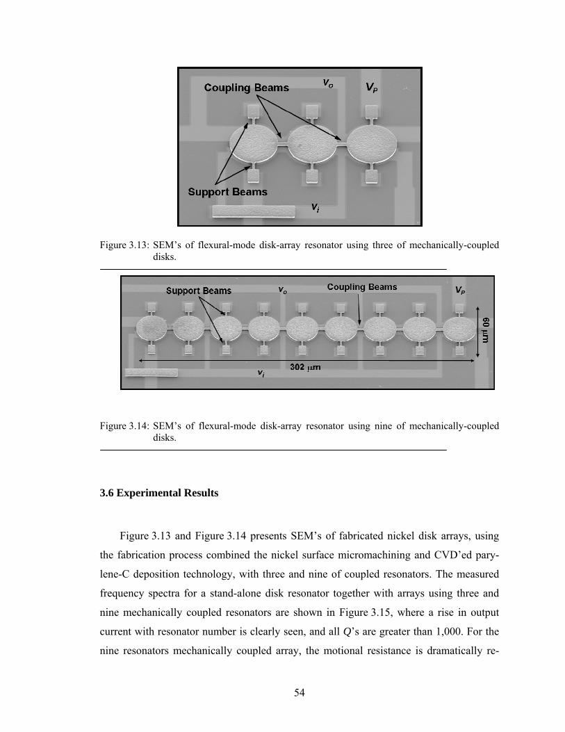
Figure 3.13: SEM’s of flexural-mode disk-array resonator using three of mechanically-coupled disks............................................................................................. 54
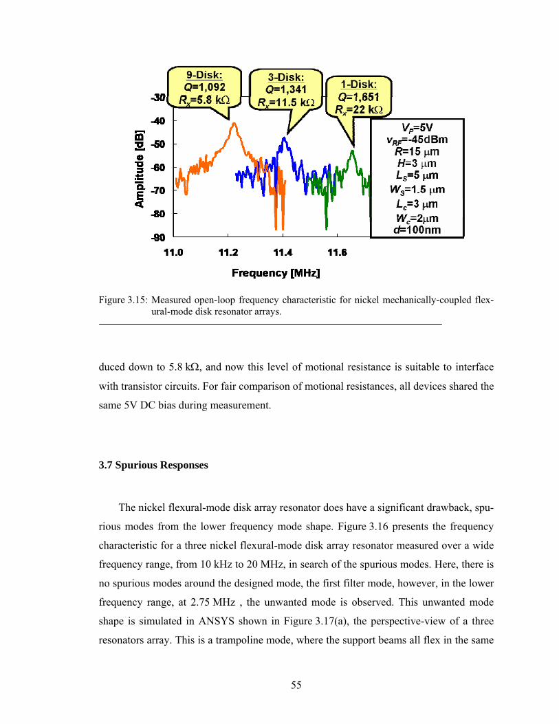
Figure 3.14: SEM’s of flexural-mode disk-array resonator using nine of mechanically-coupled disks............................................................................................. 54
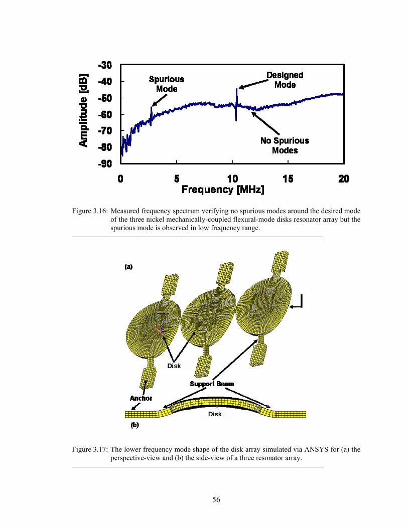
Figure 3.15: Measured open-loop frequency characteristic for nickel mechanically-coupled flexural-mode disk resonator arrays............................................ 55
Figure 3.16: Measured frequency spectrum verifying no spurious modes around the desired mode of the three nickel mechanically-coupled flexural-mode disks resonator array but the spurious mode is observed in low frequency range.......................................................................................................... 56
Figure 3.17: The lower frequency mode shape of the disk array simulated via ANSYS for (a) the perspective-view and (b) the side-view of a three resonator array. ......................................................................................................... 56
xi
Figure 3.18: A schematic of a flexural-mode single disk showing a fully differential drive and sense setup. ............................................................................... 57
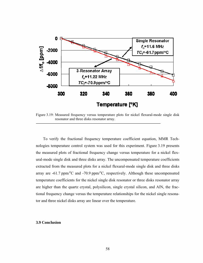
Figure 3.19: Measured frequency versus temperature plots for nickel flexural-mode single disk resonator and three disks resonator array. .............................. 58
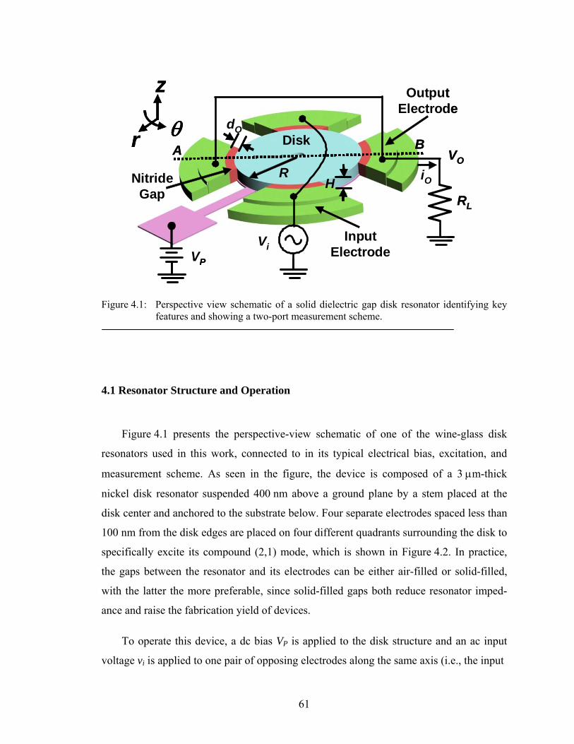
Figure 4.1: Perspective view schematic of a solid dielectric gap disk resonator identifying key features and showing a two-port measurement scheme. . 61
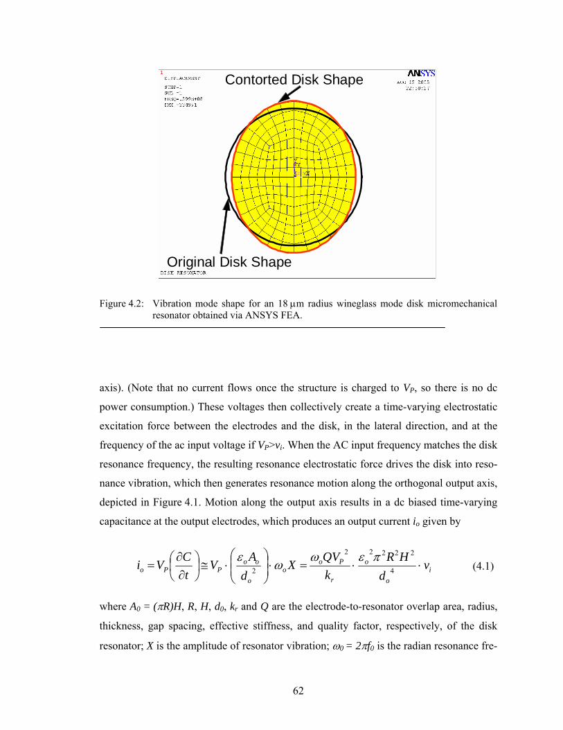
Figure 4.2: Vibration mode shape for an 18 μm radius wineglass mode disk micromechanical resonator obtained via ANSYS FEA. ........................... 62
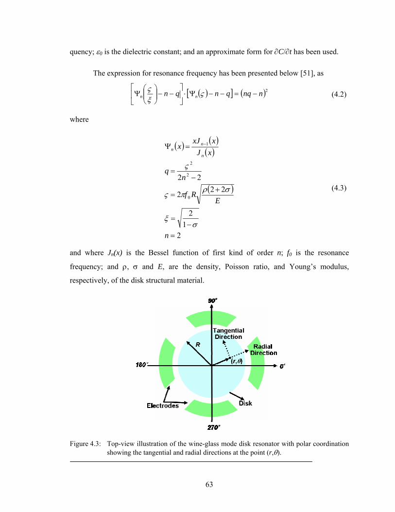
Figure 4.3: Top-view illustration of the wine-glass mode disk resonator with polar coordination showing the tangential and radial directions at the point (r,θ)................................................................................................................... 63
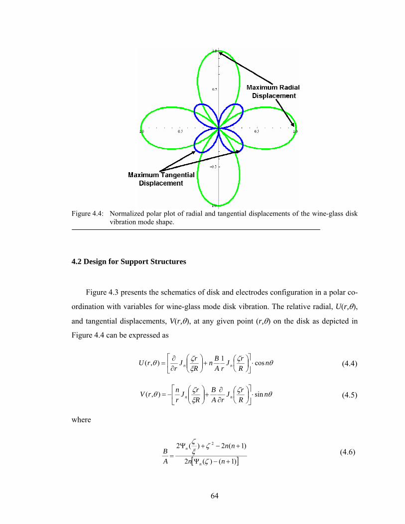
Figure 4.4: Normalized polar plot of radial and tangential displacements of the wine-glass disk vibration mode shape. .............................................................. 64
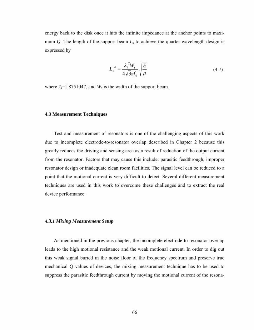
Figure 4.5: Electrical and mechanical signal plots illustrating conversion of off-resonance electrical signals at wLO and wRF down to a force at wIF. ......... 67
Figure 4.6: Schematic illustrating the mixing measurement setup, showing detailed connections between measurement instrumentations. .............................. 68
Figure 4.7: Depictions of the hook-up procedure for charge-biased measurement. (a) Charge-biasing the disk structure via a charged probe tip. (b) Electrical hook-up for mixing measurement of a charge-biased resonator............... 70
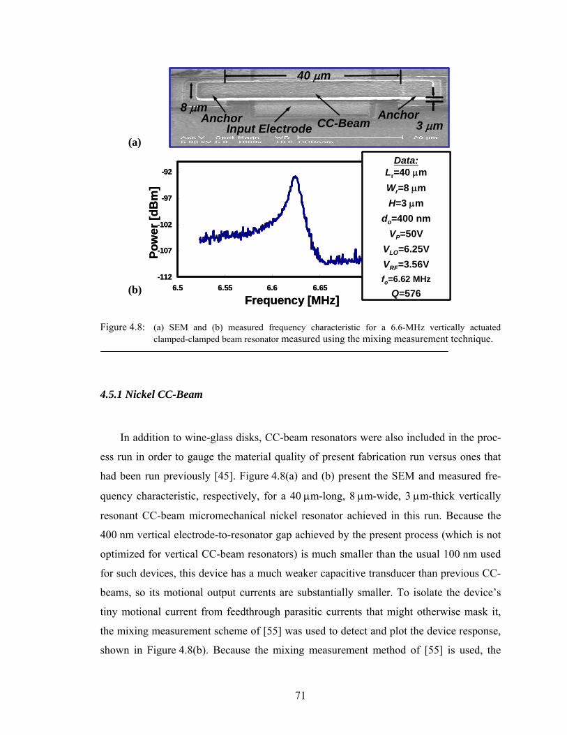
Figure 4.8: (a) SEM and (b) measured frequency characteristic for a 6.6-MHz vertically actuated clamped-clamped beam resonator measured using the mixing measurement technique. ............................................................... 71
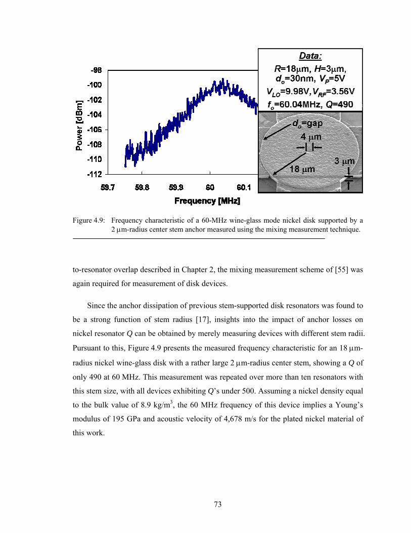
Figure 4.9: Frequency characteristic of a 60-MHz wine-glass mode nickel disk supported by a 2 μm-radius center stem anchor measured using the mixing measurement technique............................................................................. 73
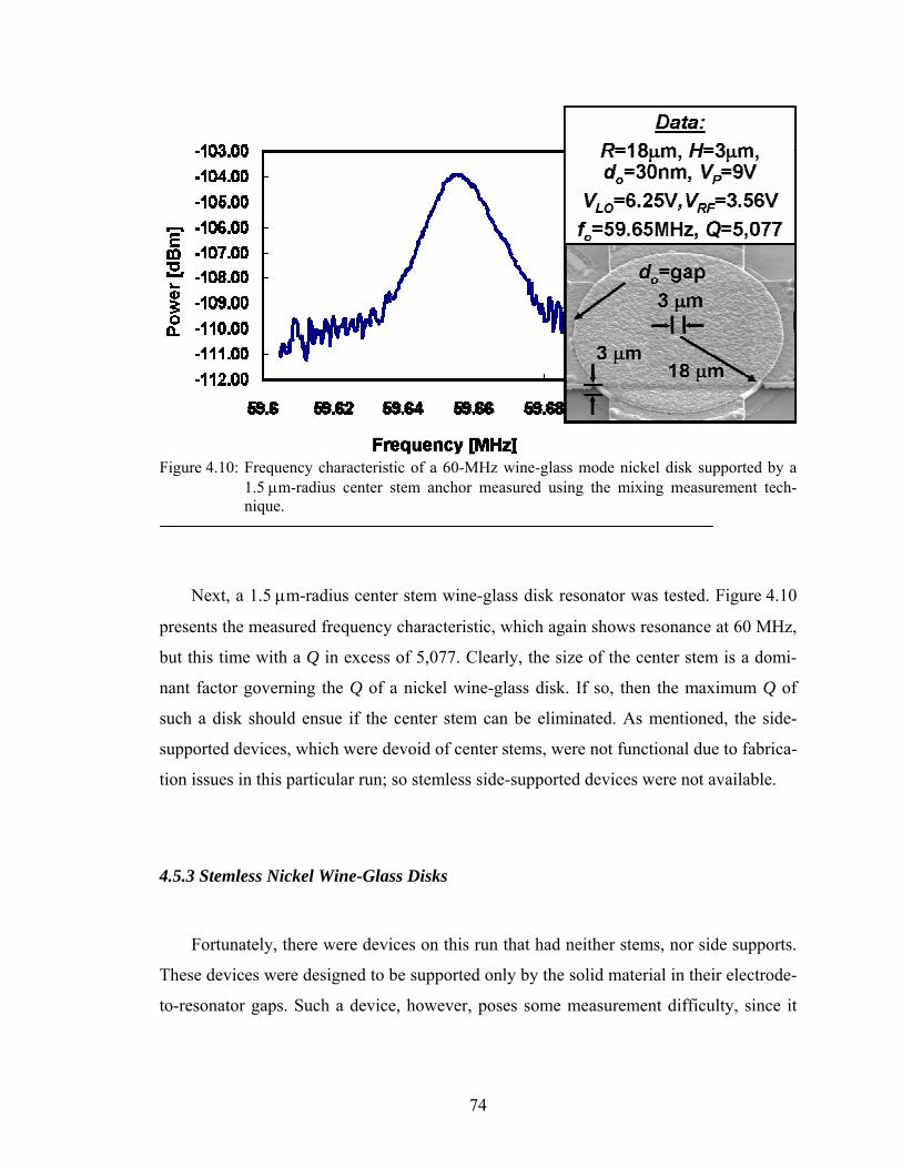
Figure 4.10: Frequency characteristic of a 60-MHz wine-glass mode nickel disk supported by a 1.5 μm-radius center stem anchor measured using the mixing measurement technique. ............................................................... 74
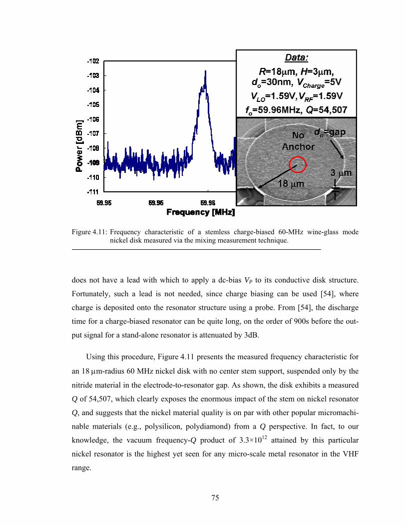
Figure 4.11: Frequency characteristic of a stemless charge-biased 60-MHz wine-glass mode nickel disk measured via the mixing measurement technique........ 75
Figure 4.12: Plot of resonance output amplitude versus discharging time for a charged-biased micromechanical nickel disk resonator.......................................... 76
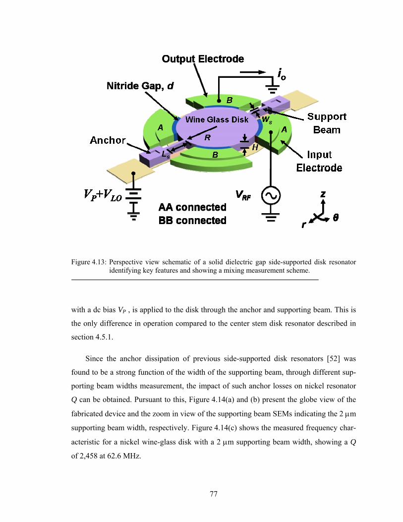
Figure 4.13: Perspective view schematic of a solid dielectric gap side-supported disk
xii
resonator identifying key features and showing a mixing measurement scheme. ..................................................................................................... 77
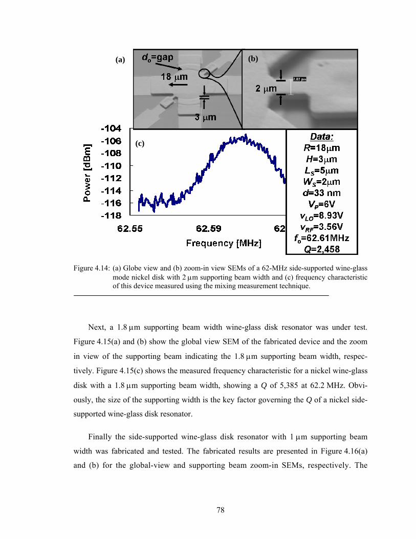
Figure 4.14: (a) Globe view and (b) zoom-in view SEMs of a 62-MHz side-supported wine-glass mode nickel disk with 2 μm supporting beam width and (c) frequency characteristic of this device measured using the mixing measurement technique............................................................................. 78
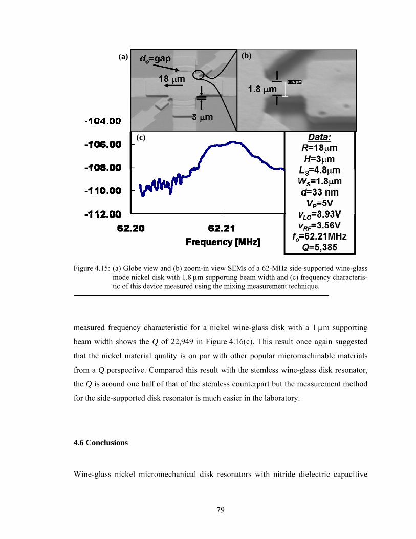
Figure 4.15: (a) Globe view and (b) zoom-in view SEMs of a 62-MHz side-supported wine-glass mode nickel disk with 1.8 μm supporting beam width and (c) frequency characteristic of this device measured using the mixing measurement technique............................................................................. 79
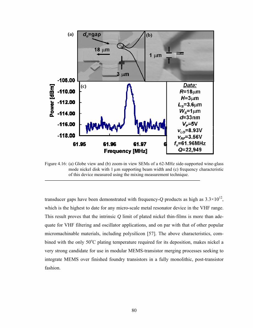
Figure 4.16: (a) Globe view and (b) zoom-in view SEMs of a 62-MHz side-supported wine-glass mode nickel disk with 1 μm supporting beam width and (c) frequency characteristic of this device measured using the mixing measurement technique............................................................................. 80
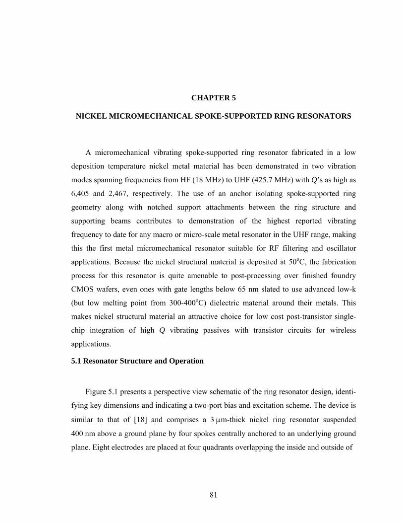
Figure 5.1: Perspective view schematic of a micromechanical spoke-supported ring resonator, identifying key dimensions and showing a typical two-port bias and excitation configuration. .................................................................... 82
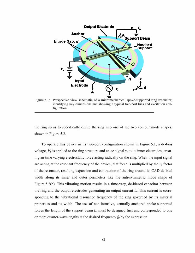
Figure 5.2: Finite element simulated (a) 1st contour mode (symmetric mode) and (b) 2nd contour mode shape (anti-symmetric mode) for the nickel ring resonator of Figure 5.1.............................................................................. 83
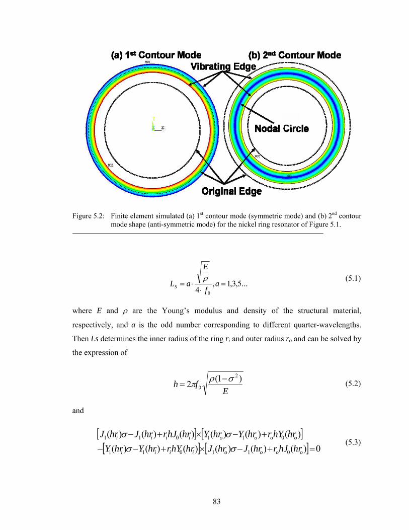
Figure 5.3: Finite element simulated mode shape for a nickel ring resonator and arrows relating points on a relative vibration displacement curve with locations on the ring.................................................................................. 85
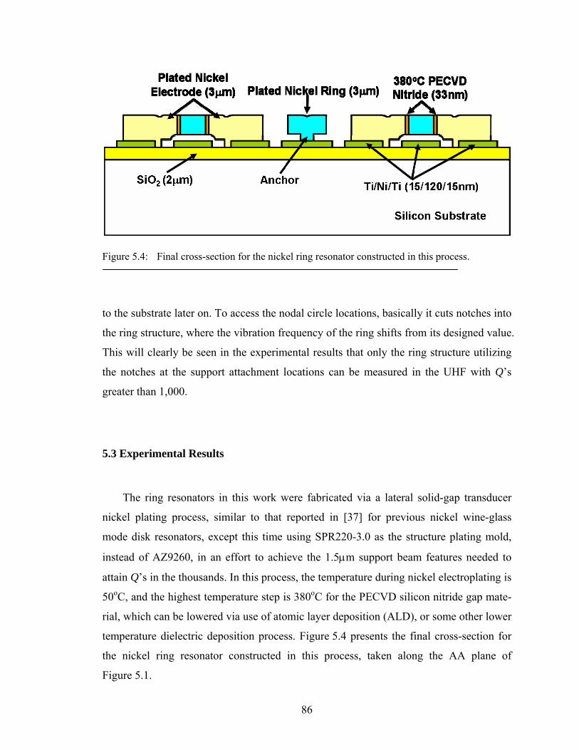
Figure 5.4: Final cross-section for the nickel ring resonator constructed in this process................................................................................................................... 86
Figure 5.5: Global-view SEM of the ring resonator and a zoom-in SEM on one of its direct support attachment locations. ......................................................... 87
Figure 5.6: Global-view SEM of the ring resonator and a zoom-in SEM on one of its notched support attachment locations....................................................... 88
Figure 5.7: Gap-zoomed SEM of the incomplete electrode-to resonator overlap....... 88
Figure 5.8: Frequency characteristic of a fabricated nickel ring resonator with direct support attachments operated at its first radial contour mode centered at 20.2 MHz, measured via a mixing measurement technique. .................... 89
Figure 5.9: Frequency characteristic of a fabricated nickel ring resonator with notched support attachments operated at its first radial contour mode centered at 18 MHz, measured via a mixing measurement technique. ....................... 89
xiii
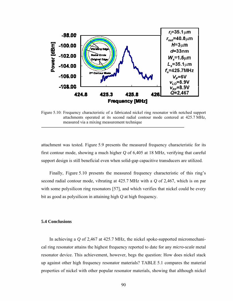
Figure 5.10: Frequency characteristic of a fabricated nickel ring resonator with notched support attachments operated at its second radial contour mode centered at 425.7 MHz, measured via a mixing measurement technique ................... 90
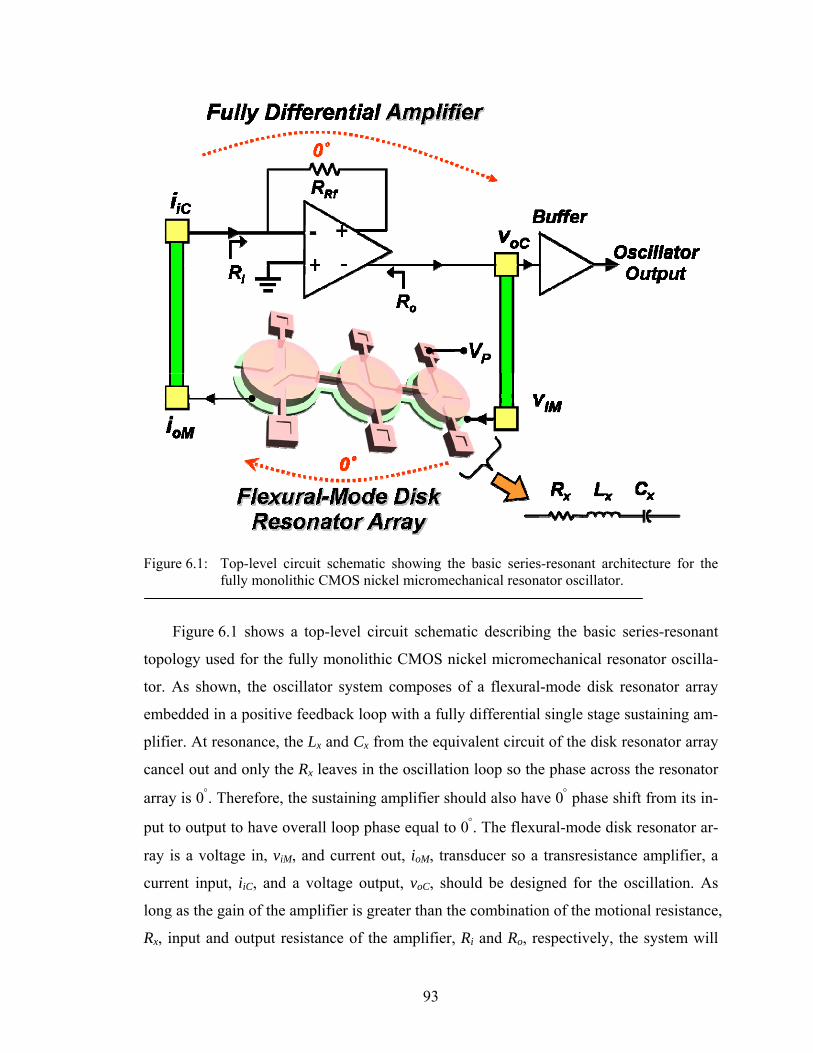
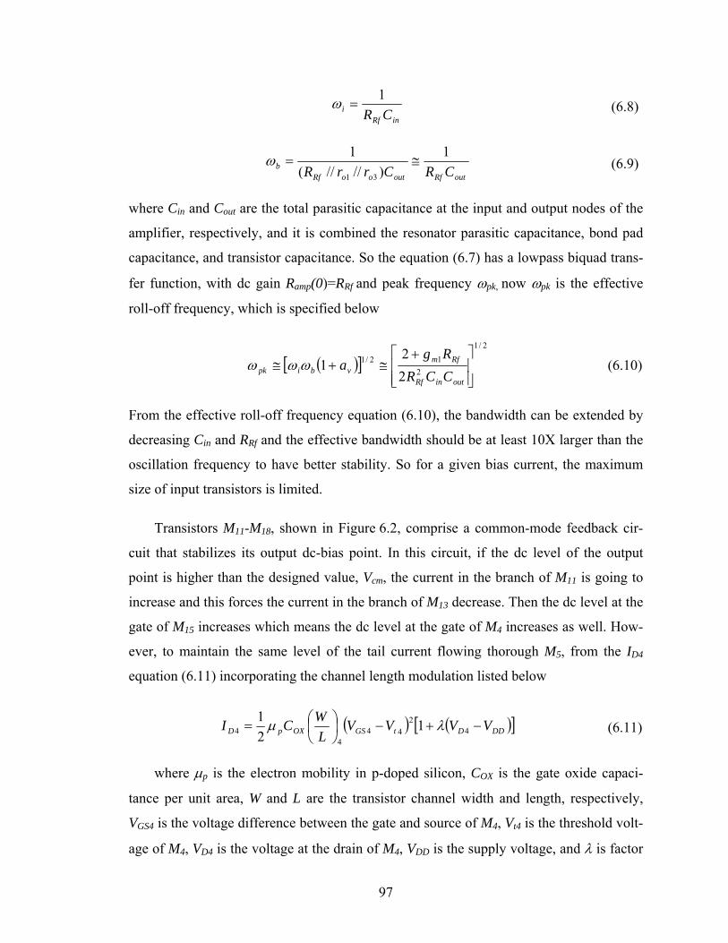
Figure 6.1: Top-level circuit schematic showing the basic series-resonant architecture for the fully monolithic CMOS nickel micromechanical resonator oscillator.................................................................................................... 93
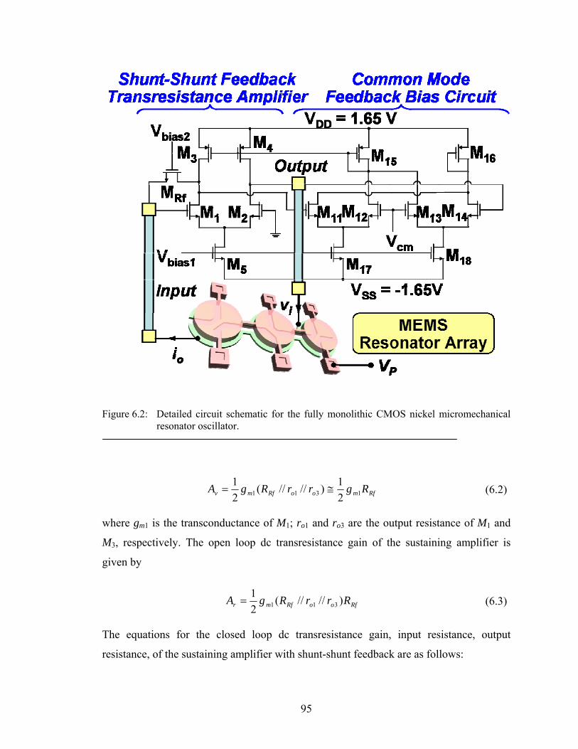
Figure 6.2: Detailed circuit schematic for the fully monolithic CMOS nickel micromechanical resonator oscillator. ...................................................... 95
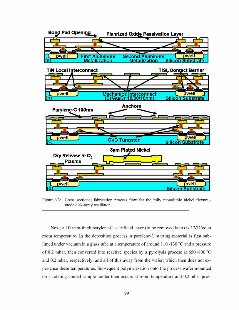
Figure 6.3: Cross sectional fabrication process flow for the fully monolithic nickel flexural-mode disk-array oscillator. .......................................................... 99
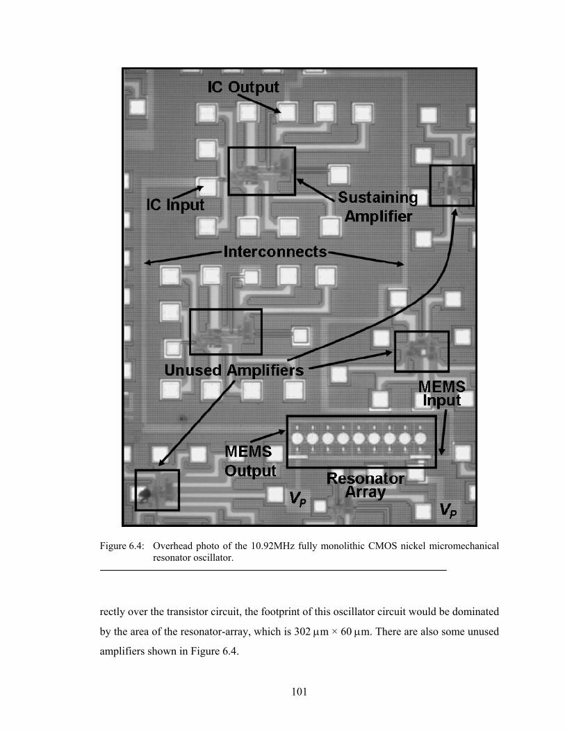
Figure 6.4: Overhead photo of the 10.92MHz fully monolithic CMOS nickel micromechanical resonator oscillator. .................................................... 101
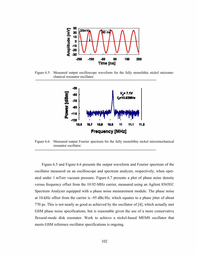
Figure 6.5: Measured output oscilloscope waveform for the fully monolithic nickel micromechanical resonator oscillator. .................................................... 102
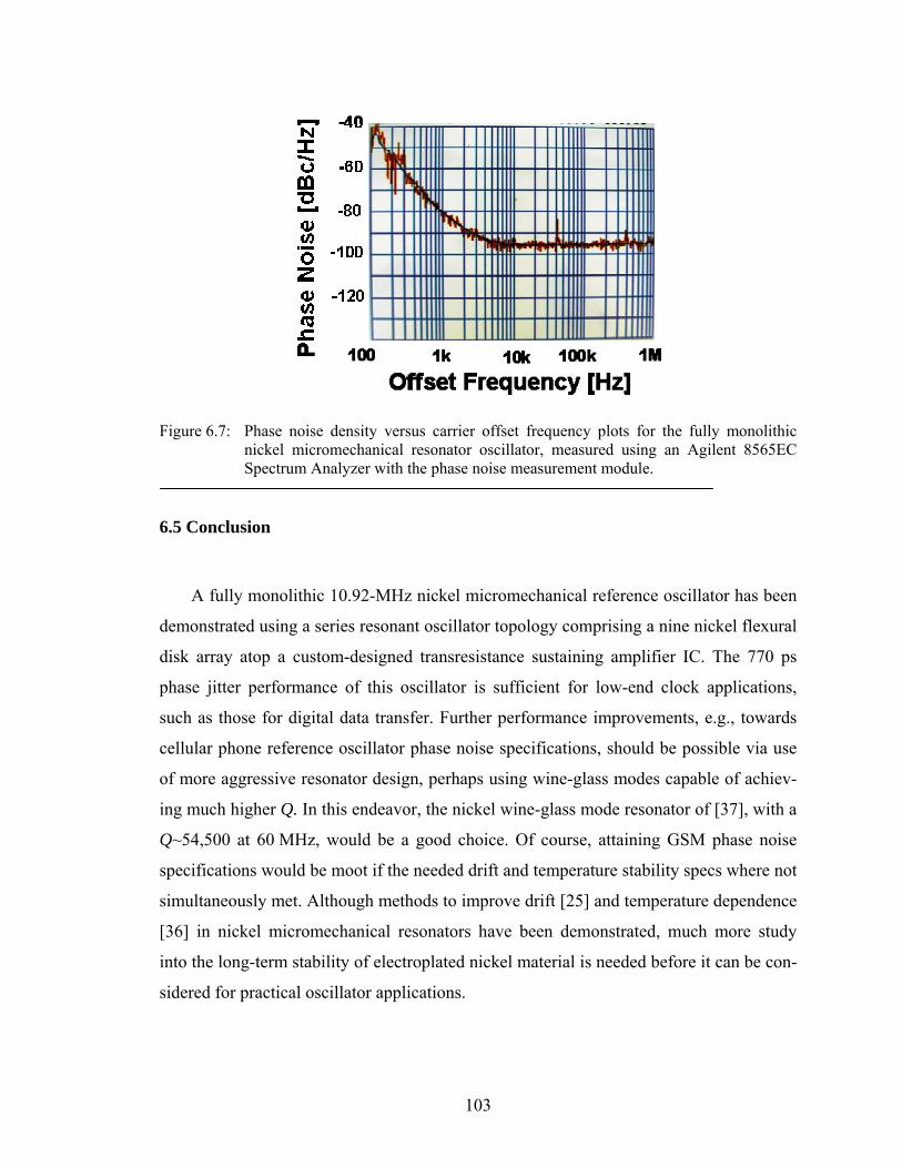
Figure 6.6: Measured output Fourier spectrum for the fully monolithic nickel micromechanical resonator oscillator. .................................................... 102
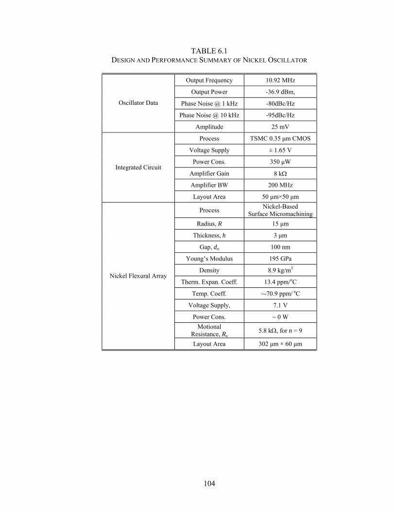
Figure 6.7: Phase noise density versus carrier offset frequency plots for the fully monolithic nickel micromechanical resonator oscillator, measured using an Agilent 8565EC Spectrum Analyzer with the phase noise measurement module. ................................................................................................... 103
xiv
LIST OF TABLES
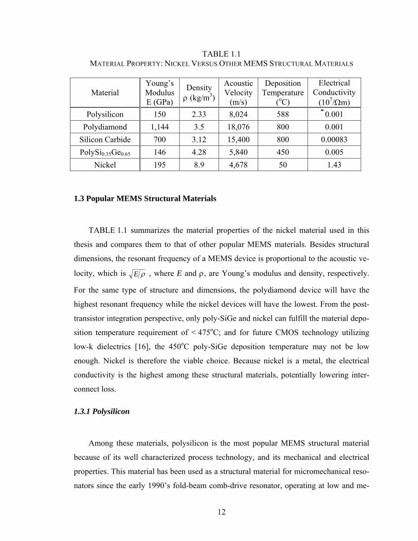
TABLE 1.1 Material Property: Nickel Versus Other MEMS Structural Materials...... 12
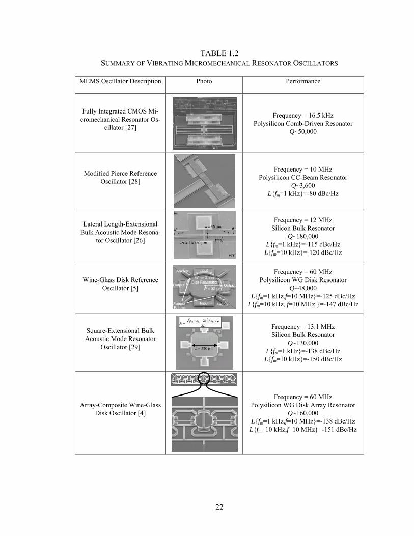
TABLE 1.2 Summary of Vibrating Micromechanical Resonator Oscillators ............. 22
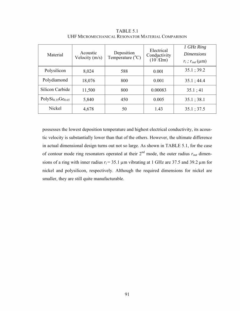
TABLE 5.1 UHF Micromechanical Resonator Material Comparison......................... 91
TABLE 6.1 Design and Performance Summary of Nickel Oscillator ....................... 104
xv
ABSTRACT
FULLY MONOLITHIC CMOS NICKEL MICROMECHANICAL RESONATOR OSCILLATOR FOR WIRELESS COMMUNICATIONS
by
Wen-Lung Huang
Co-Chairs: Clark T.-C. Nguyen and Michel M. Maharbiz
A nickel surface-micromachining technology offering various electrode-to-resonator
gap materials is presented that is particularly suitable for high-Q, low impedance MEMS-
based vibrating resonators. The low temperature of this nickel fabrication technology
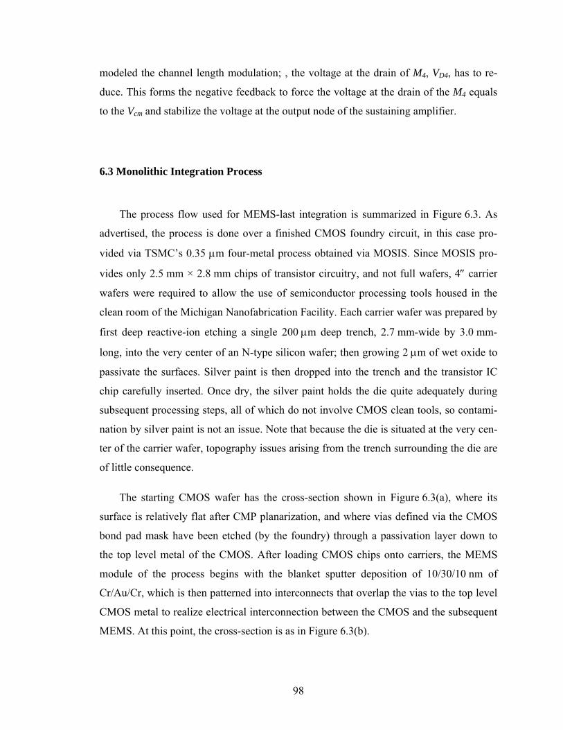
makes it amenable to post-processing over finished foundry CMOS wafers, even those
using advanced low-k, low temperature dielectrics around metallization to decrease inter-
connect capacitance. Such a MEMS-last process technology is used in this work to dem-
onstrate a fully monolithic MEMS-based oscillator comprised of a nickel disk resonator
array surface-micromachined over foundry CMOS.
To achieve resonator motional resistances below 5.8 kΩ with adequate quality factor,
a mechanically-coupled array of resonators is used that actually realizes a multi-pole fil-
ter structure, from which a single mode can be selected and other modes can be sup-
pressed by proper electrode phasing. To attain higher frequencies, a nickel wine-glass
xvi
mode disk resonator with a nitride capacitive transducer gaps was demonstrated at fre-
quencies approaching 60 MHz with Q’s as high as 54,507, which is the highest to date for
any micro-scale metal resonator in the VHF range. To boost frequencies to the UHF
range, vibrating nickel micromechanical spoke-supported ring resonators were demon-
strated at 425.7 MHz with Q’s as high as 2,467. These devices employed an anchor iso-
lating spoke-supported ring geometry along with notched support attachments between
the ring structure and supporting beams to achieve the highest reported vibrating fre-
quency to date for any micro-scale metal resonator.
Finally, a fully monolithic oscillator was achieved using MEMS-last integration to
fabricate a resonator array of nine nickel flexural-mode disks over foundry CMOS cir-
cuitry. The oscillator demonstrated a measured phase noise of -95 dBc/Hz at a 10 kHz
offset from its 10.92-MHz carrier frequency, which is adequate for some low-end timing
applications. This, together with its low power consumption of 350 μW, and the potential
for full integration of integrated circuits and MEMS devices onto a single chip, makes the
dium frequency ranges with Q~50,000 under vacuum conditions. Polysilicon is also used
in the recently self-aligned contour mode disk resonator, operating at 1.14 GHz with Q
~1,595 and 1,583 measured in vacuum and air, respectively, shown in Figure 1.9 [17].
Figure 1.9: Measured (dark) and predicted (light) frequency characteristic for a 1.14-GHz, 3rd
mode, 10 μm radius polysilicon disk resonator measured in (a) vacuum and (b) air. (c) SEM of the fabricated disk resonator after HF release [17].
Figure 1.10: (a) and (b) are SEMs of a fabricated 1.2-GHz polysilicon hollow-disk ring resonator
without notched and with notched supports, respectively. (c) and (d) are frequency characteristics measured in vacuum [18].
(c)
(a) (b)
(c) (d)
14
Figure 1.11: (a) Frequency characteristics measured in air and (b) SEM of a fabricated 1.5-GHz
2rd mode, 10-μm radius polydiamond disk resonator with material-mismatched iso-lating support [20].
The contour-mode disk can operate at UHF. However, because of its anchor design
and size, its Q is below 10,000 and is therefore not suitable for the RF channel-selection
filter application. With the same structural material but different supporting beam design,
the hollow-disk ring resonator with the notched supporting beam, also using the self-
aligned process, raises the Q to 14,603 at 1.2 GHz as shown in Figure 1.10 [18]. So with
the optimization of supporting beam design and right device structure, the polysilicon
resonator still can achieve a Q > 10,000 at over 1-GHz.
1.3.2 Polydiamond
Ideal polydiamond has a high acoustic velocity of 18,076 m/s [19], which is 2.25X
and 1.57X greater than the acoustic velocity of single crystal silicon and silicon carbide,
respectively. From use in a high frequency device, polydiamond is a good candidate.
In the previous polydiamond folded-beam resonator [19], the Q is 36,460 at
27.3 kHz and its Q is on par with the polysilicon version. Also, the Q of the polydiamond
clamped-clamped beam resonators [20] are comparable to values seen in the polysilicon
versions. The polydiamond micromechanical disk resonators with material-mismatched
isolating support [20] operated at 498 MHz, has Q’s up to 55,300 and 35,550 in vacuum
and air, respectively, and still holds frequency-Q product record at 2.75x10¹³ (vacuum)
and 1.77x10¹³ (air). In Figure 1.11, the measured frequency characteristic for a 10-μm
(a) (b)
15
Figure 1.12: (a) Poly-SiC Lamé-mode resonator with 195nm FIB-cut transducer gap. (b) The measured frequency characteristic using the fully differential electrode configuration [22].
radius diamond disk with 0.8 μm-radius stem, operating in second radial-contour mode at
1.51 GHz with Q’s of 10,100 in air on par with that in vacuum. At 1.51 GHz, 0.8 μm-
radius stem is not the optimum stem size design so higher Q should be able to attain with
the optimum stem design.
1.3.3 Silicon Carbide
Silicon carbide is an attractive structural material for RF MEMS and NEMS
application due to its relatively high acoustic velocity, 15,400 m/s and stable
physiochemical properties. The material properties of silicon carbide are better known
compared to that of polydiamond.
However, silicon carbide has low electrical conductivity resulting in a several MΩ
resistance in the resonator suspension. Also, the anchor degraded the measured Q of the
resonators. To accurately extract the real Q of SiC, either a thin layer of aluminum may
be deposited on top of the resonator [21] or the fully differential electrode configuration
[22] may be employed to reduce the electrical dissipative losses and enable the true mate-
rial Q to be measured. The SEM presented in Figure 1.12(a) is the poly-SiC Lamé reso-
nator [22] using a Focused Ion Beam (FIB) to cut through the structure and electrodes, to
form the electromechanical transducer gap. The measured frequency characteristic is
shown in Figure 1.12(b) with Q’s of 9,300 at 173.5 MHz.
(a) (b)
16
Figure 1.13: (a) SEM and (b) frequency characteristic measured in air of a poly-SiGe disk resona-
tor [23].
1.3.4 Silicon Germanium
The poly-SiGe material can be deposited at 450oC and it has been demonstrated that
it can be integrated with a CMOS transistor circuit using the post-transistor integration
method [15] at very low frequency.
Despite its relatively low acoustic velocity, 5,840 m/s, a poly-SiGe disk resonator re-
cently has been developed with Q’s of 15,300 at frequency up to 425 MHz [23]. The
SEM and frequency characteristic of the poly-SiGe disk are shown in Figure 1.13(a) and
(b).
From these data, the poly-SiGe resonators are shown to have performance compara-
ble with polysilicon disks but its long term stability is around -1~-2 ppm/day compared to
the polysilicon resonator on the order of 0.5 ppm/year [24] still quite large. A slope direc-
tion change from negative to positive is also reported in [23]. However, a physical expla-
nation has not been proposed.
(a) (b)
17
Figure 1.14: (a) SEM and (b) frequency characteristic measured in vacuum of a nickel comb-
driven resonator [25].
1.3.5 Electroplated Nickel
Despite the Q and drift problems encountered in early attempts to use nickel as a
structural material in MEMS devices, efforts to improve the material continued, spurred
by its great potential for post-transistor planar integration. In 1999, work by Hsu and
Nguyen [25] introduced a method dubbed “in situ localized annealing”, where an electri-
cal current is sent through the conductive mechanical structure of a resonator device to
heat it to temperatures as high as 886oC while vibrating the device at its resonant fre-
quency. Application of this method to 75-kHz folded-beam resonators was found to raise
their Q’s from 4,103 to 14,172, shown in Figure 1.14(b), and to greatly improve their
drift stability. In principle, operation of the resonator device at high temperature was
thought to redistribute or remove defects and contaminants from its volume and surfaces,
effectively removing intrinsic loss mechanisms, thereby allowing much higher Q and sta-
bility.
Later attempts in 1999 were not successful to apply localized annealing to higher
frequency clamped-clamped beam (“CC-beam”) and free-free beam (“FF-beam”) resona-
tors made in nickel structural material, however. In particular, only CC-beam devices
were functional in the fabrication run devoted to this evaluation, and these yielded Q’s on
the order of only 532. The FF-beam devices, which were much better isolated from their
(a)
18
anchors, were unfortunately not functional. Thus, at the time this work was discontinued
shortly after 2000, and it was uncertain whether the low Q’s of VHF CC-beam nickel
resonators were caused by anchor loss mechanisms or intrinsic material loss mechanisms.
1.4 MEMS Oscillators
In the present wireless communication transceiver, the bulky quartz crystal oscillator
used as the timing reference is one of the most difficult devices to miniaturize. So far, no
on-chip counterparts can match its performances of quality factor and temperature stabil-
ity. Recently, the vibrating micromechanical resonators based on the capacitively-
transduced surface-micromachined technology have the comparable performances, for
example, wine-glass disk resonators with Q’s exceeding 160,000 in vacuum, square-
extensional mode and lateral length-extensional single-crystal silicon resonators with Q’s
up to 130,000 and 180,000, respectively. MEMS oscillators based on each of the above
resonators have been demonstrated [4][5][26][29]. Despite some of them meeting the
GSM phase noise specifications of -130 dBc/Hz at 1 kHz offset from a 13 MHz carrier
and -150 dBc/Hz at far-from-carrier offsets, until now, none of these oscillators have
clear paths for future fully integrated versions. This thesis demonstrates the fully mono-
lithic CMOS nickel resonator oscillator utilizing the low deposition temperature of nickel
structural material and the MEMS-last integration approach, detailed in Chapter 6.
In the present section, the fundamentals for the series-resonant oscillator are
introduced, and previous works of MEMS oscillators are summarized.
1.4.1 Series –Resonant Oscillator Fundamentals
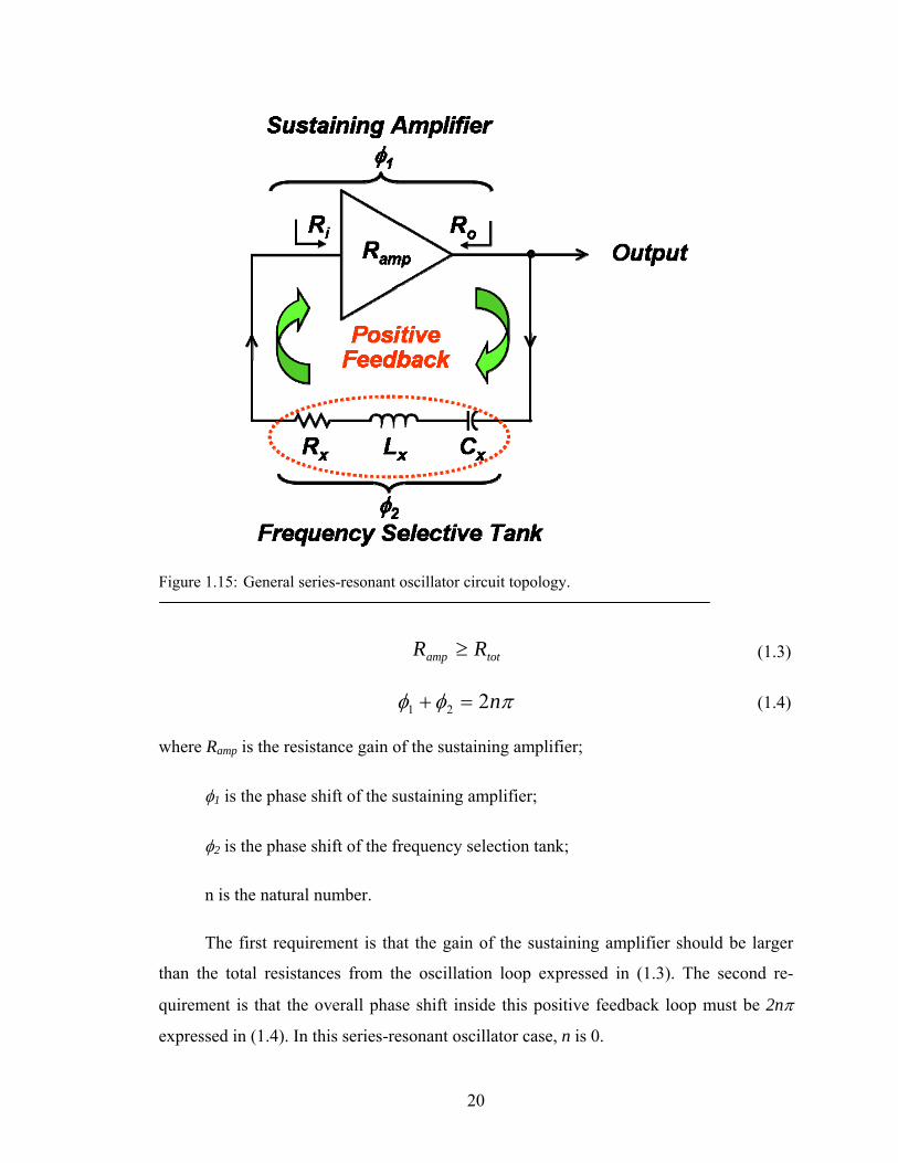
Figure 1.15 presents the top-level schematic of the oscillator circuit based on the se-
ries-resonant oscillator topology used in this thesis. The micromechanical resonators have
a voltage-in and current-out transfer function so the sustaining amplifier has to be de-
19
signed as the transresistance amplifier.
There are two advantages of using the transresistance amplifier: (1) better accommo-
dation of the relatively larger motional resistance of the resonator (~several kΩ), and (2)
small input and output resistances to retain the resonator’s high Qload as expressed in (1.1)
where Ri and Ro are the input and output resistances of the amplifier;
Rx is the motional resistance of the resonator;
Rtot is the total resistance within the oscillation loop;
Qresoantor is the unloaded Q of the resonator.
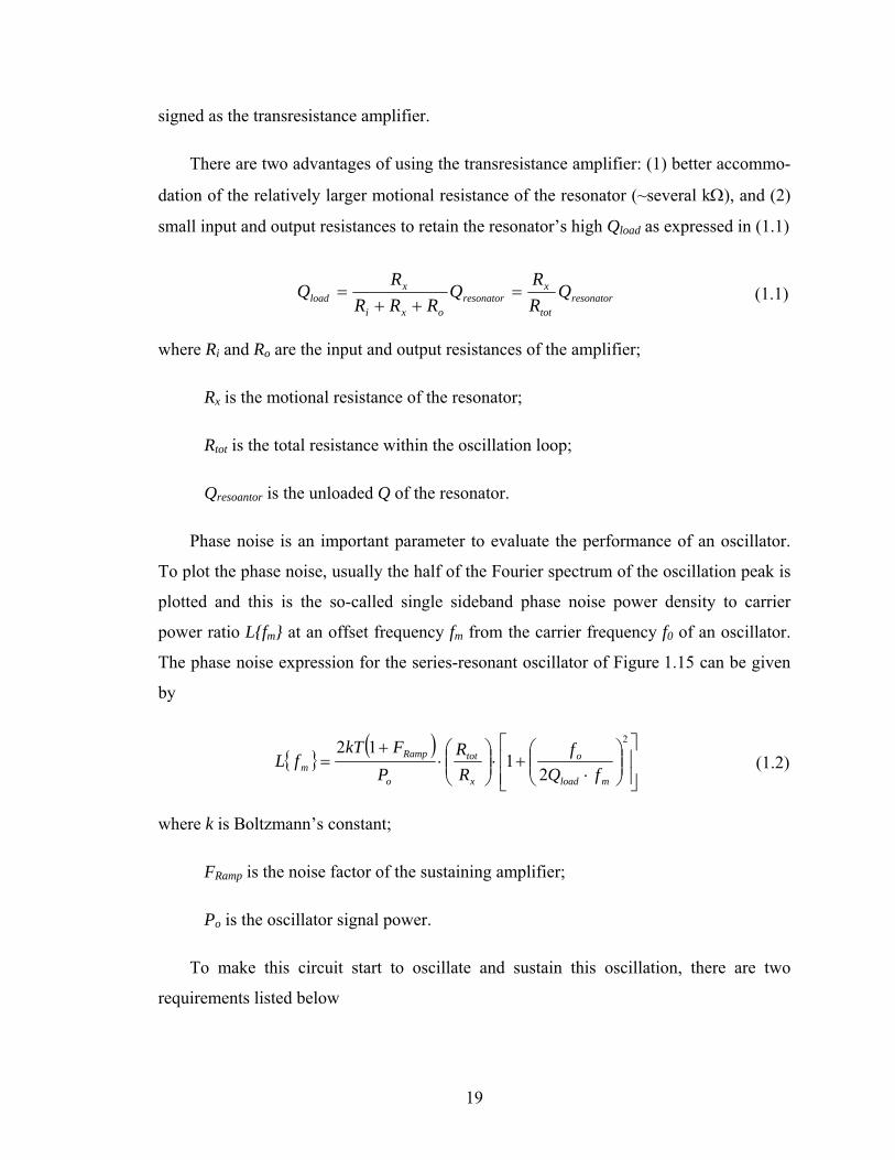
Phase noise is an important parameter to evaluate the performance of an oscillator.
To plot the phase noise, usually the half of the Fourier spectrum of the oscillation peak is
plotted and this is the so-called single sideband phase noise power density to carrier
power ratio L{fm} at an offset frequency fm from the carrier frequency f0 of an oscillator.
The phase noise expression for the series-resonant oscillator of Figure 1.15 can be given
by
{ } ( )⎥⎥⎦
⎤
⎢⎢⎣
⎡⎟⎟⎠
⎞⎜⎜⎝
⎛⋅
+⋅⎟⎟⎠
⎞⎜⎜⎝
⎛⋅
+=
2
21
12
mload
o
x
tot
o
Rampm fQ
fRR
PFkT
fL (1.2)
where k is Boltzmann’s constant;
FRamp is the noise factor of the sustaining amplifier;
Po is the oscillator signal power.
To make this circuit start to oscillate and sustain this oscillation, there are two
requirements listed below
resonatortot
xresonator
oxi
xload Q
RR
QRRR
RQ =
++= (1.1)
20
Figure 1.15: General series-resonant oscillator circuit topology.
where Ramp is the resistance gain of the sustaining amplifier;
φ1 is the phase shift of the sustaining amplifier;
φ2 is the phase shift of the frequency selection tank;
n is the natural number.
The first requirement is that the gain of the sustaining amplifier should be larger
than the total resistances from the oscillation loop expressed in (1.3). The second re-
quirement is that the overall phase shift inside this positive feedback loop must be 2nπ
expressed in (1.4). In this series-resonant oscillator case, n is 0.
totamp RR ≥ (1.3)
πφφ n221 =+ (1.4)
21
1.4.3 MEMS Reference Oscillator
Previous work on MEMS oscillators is summarized in TABLE 1.2. C. T.-C. Nguyen
demonstrated the first fully-integrated MEMS oscillator utilizing a comb-drive resonator
fabricated along side with an integrated circuit on a single chip in 1993. Despite its fully
integration, the oscillation frequency was only operated at 16.5 kHz not sufficient for any
wireless communication applications.
After this fully-integrated MEMS oscillator, research in the MEMS oscillator ceased
until 2001. S. Lee implemented his MEMS oscillator by combining the clamped-clamped
beam resonator with off-chip amplifiers to make a modified Pierce oscillator. This
oscillator operated at 10 MHz, sufficient for the communication systems, however, its
phase noise performances did not have adequate values. This is because the power
handling and Q of the clamped-clamped beam resonator are not high enough to meet the
GSM phase noise performance.
In 2002, T. Mattila demonstrated a bulk acoustic mode silicon micromechanical
resonator wire bonded a discrete amplifier on the board level to form a MEMS oscillator
with 12-MHz operating frequency. Despite the resonator’s high Q, 180,000, the phase
noise performance was still short of the GSM specifications. Besides this, the fabrication
process for this resonator is bulk micromachining and it is very difficult to fully integrate
with MEMS deices with transistor circuits.
In 2004, Y.-W. Lin used a wine-glass disk resonator with the custom-designed sin-
gle-stage zero-phase-shift sustaining amplifier and it barely satisfied the GSM phase
noise specification. The same year, V. Kaajakari demonstrated a micromechanical 13.1-
MHz bulk acoustic mode silicon resonator combined with a discrete amplifier to make a
MEMS oscillator that meets the GSM phase noise specifications.
22
TABLE 1.2 SUMMARY OF VIBRATING MICROMECHANICAL RESONATOR OSCILLATORS
Seed layer removed; Nitride serves as one side of mold
Silicon Substrate
(e’)
(f) Silicon Substrate
After Release in NaOH
Nitride Gap
(f) Silicon Substrate
After Release in NaOH
Nitride Gap
(d) Silicon Substrate
Nickel Seed Layer (20nm)PR Etchback PR Etchback
(d’)(d) Silicon Substrate
Nickel Seed Layer (20nm)PR Etchback PR Etchback
(d’)
Electroplated Nickel (3μm)
(e)
Seed layer removed; Nitride serves as one side of mold
Silicon Substrate
(e’)
Electroplated Nickel (3μm)
(e)
Seed layer removed; Nitride serves as one side of mold
Silicon Substrate
(e’)
Figure 2.6: Cross sectional fabrication process flow and associated SEM’s for laterally vibrating
nickel disk resonators with a solid dielectric gap
39
Output Electrode
R=18 μm
Anchor
Electrode
DiskResonator
30nm Nitride GapInputElectrode
Output Electrode
R=18 μm
Anchor
Electrode
DiskResonator
30nm Nitride GapInputElectrode
Figure 2.7: (a) Globe-view and (b) gap-zoomed SEM’s of a fabricated nickel disk resonator
supported by a stem anchored at its center.
Usually in the polysilicon disk process, either low pressure chemical vapor
deposition (LPCVD) high temperature silicon oxide or silicon nitride is used for air gap
and solid gap devices, respectively. Those materials are grown in the furnace tube under
the low process condition so the step coverage is conformal and their qualities are good
(no pin holes). However in the nickel resonator process described in the previous section,
those metals used for interconnect or structure cannot sustain those deposition
temperatures in the LPCVD steps. Instead of LPCVD, plasma enhanced chemical vapor
deposition (PECVD) nitride is used as the gap material and with this kind of gap material,
the step coverage and pin holes need to be reevaluated. According to process experience,
if the final electrode plating material changes from nickel to gold and 30-nm PECVD
nitride is used; all of the devices are shorted from the electrodes to the structure. This
phenomenon can be caused by either a lack of conformability or pin holes. In the future,
the PECVD nitride should be replaced with other high-k dielectrics that have better film
quality and step coverage.
(b)
(a)
40
2.4 Conclusions
A nickel surface micromachining technology combined with the parylene-C is
utilized to fabricate the flexural mode disk array device. This fabrication technology
really lowers down the devices’ impedance to a degree that those fabricated devices can
fully integrate on top of the integrated circuits. And a nickel surface micromachining
technology combined with the “solid” gap is also developed. This “solid” gap technology
demonstrated not only the highest Q in VHF range but also the highest reported vibrating
frequency ever measured to date for any macro- and micro-scale metal resonator.
41
CHAPTER 3
MECHANICALLY COUPLED NICKEL FLEXTURAL MODE N DISK-ARRAY RESONATORS
A nickel flexural-mode disk micromechanical resonator that utilizes a stemless, non-
intrusive suspension structure operates at HF range with Q’s >1,000. At the beginning,
the sputtered aluminum was used as the sacrificial layer; however, the conformability
issue not only hinders the progression of scaling down the gap from reducing the
motional impedance but also causes the spurious modes of the disk-array. To circumvent
these two issues, the sputtered aluminum sacrificial layer is replaced with the conformal
and pin-hole free parylene-C film.
Despite using the sacrificial parylene-C layer, the motional resistance of a single disk
resonator is still too high to interface with oscillator circuits. A mechanical coupled
flexural-mode disk array was designed to improve the motional resistance to a point
where disk array resonators constituted nine mechanically-coupled disks can now be fully
integrated with the transistor circuit to form the oscillation functionality presented in
Chapter 6. By mechanically coupling disk resonators, all of the disks vibrate at exactly
the same frequency and the array acts like a single resonator while still maintaining a
Q >1,000.
3.1 Resonator Structure and Operation
Figure 3.1(a) presents the perspective view schematic of a flexural-mode disk reso-
nator, connected in the typical a two-port bias excitation and measurement scheme. As
shown in this figure, the device consists of a 3 μm-thick nickel disk resonator suspended
100 nm above the input and output electrodes by two side-supported beams. These sup-
porting beams are placed at the disk’s nodal lines and anchored to the substrate
42
Figure 3.1: (a) Perspective-view schematic of a flexural mode disk micromechanical resonator
in a two-port bias configuration and (b) its top-view illustration with polar coordina-tion.
(a)
(b)
43
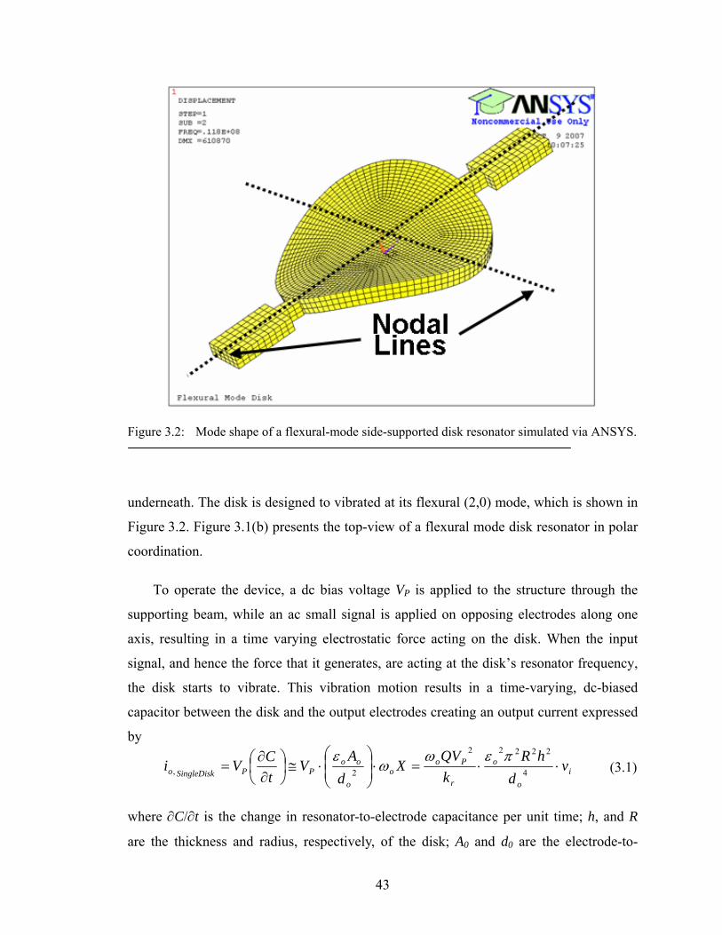
Figure 3.2: Mode shape of a flexural-mode side-supported disk resonator simulated via ANSYS.
underneath. The disk is designed to vibrated at its flexural (2,0) mode, which is shown in
Figure 3.2. Figure 3.1(b) presents the top-view of a flexural mode disk resonator in polar
coordination.
To operate the device, a dc bias voltage VP is applied to the structure through the
supporting beam, while an ac small signal is applied on opposing electrodes along one
axis, resulting in a time varying electrostatic force acting on the disk. When the input
signal, and hence the force that it generates, are acting at the disk’s resonator frequency,
the disk starts to vibrate. This vibration motion results in a time-varying, dc-biased
capacitor between the disk and the output electrodes creating an output current expressed
by
io
o
r
Poo
o
ooPPSingleDisko v
dhR
kQV
Xd
AV
tCVi ⋅⋅=⋅⎟
⎟⎠
⎞⎜⎜⎝
⎛⋅≅⎟
⎠⎞
⎜⎝⎛
∂∂
= 4
22222
2,πεω
ωε
(3.1)
where ∂C/∂t is the change in resonator-to-electrode capacitance per unit time; h, and R
are the thickness and radius, respectively, of the disk; A0 and d0 are the electrode-to-
44
resonator overlap area and static gap spacing, respectively; ε0 is the permittivity in vac-
uum; ω0=2πf0 is the radian resonance frequency; X is the amplitude of disk vibration; and
kr is the effective stiffness of the resonator.
As indicated in Figure 3.2, the mode shape of this flexural-mode side-supported disk
resonator has two nodal lines and two supporting beams that are attached to one of the
nodal lines. This supporting beam design is to minimize the energy losses to the substrate
and to maximum the high-Q operation.
3.2 Resonant Frequency Characteristics
The nominal resonance frequency fnom for a flexural mode disk resonator is governed
by [44]
ρE
Rhfnom 2253.0= (3.2)
where E and ρ are the Young’s modulus, and density, respectively, of its structural
material. The dc bias dependence of resonance frequency arises from a VP-dependent
electrical spring constant ke that subtract from the mechanical spring constant km and
yields the resonance frequency to the expression
m
enom
m
em
r
m
r
r
kk
fk
kkmk
mkf −=
−== 1
21
21
0 ππ (3.3)
where km and mr denote values at a particular location, so < ke/km> has to integrate over
the electrode area due to km’s location dependence.
The equation of < ke/km> is given by
[ ]∫∫ + ⋅=
outin AAm
oP
m
e drdrkrd
rVkk
2 3
2
),(),(θ
θθε
(3.4)
where Ain and Aout are the regions of overlap of the disk with its input and output elec-
45
trodes, respectively, as shown in Figure 3.1(b); d(r,θ) is the electrode-to-resonator gap
spacing which varies as a function of (r,θ) on the resonator due to the statically VP-
derived force that deflects the disk; km(r,θ) is the vertical stiffness when VP = 0 at a loca-
tion (r,θ) on the disk, which is given by
[ ] ),(2),( 2 θπθ rmfrk rnomm = (3.5)
where mr(r,θ) is the equivalent mass at a location (r,θ) on the disk and can be expressed
as [45]
[ ]
[ ][ ]2
),(
0 0
2),(
2 ),(
),(
),(21),(
θ
θθρ
θνθ
θ
rZ
drdrrZh
r
KErmnm
r
nmtotr
∫ ∫ ′′== (3.6)
where KEtot is the total kinetic energy in a vibrating disk; v(r,θ) is the velocity magnitude
at location (r,θ); Z(m,n)(r,θ) is the mode shape of the flexural-mode disk device and can be
expressed as [46]
)cos()()(),( ),(),(
),(),( θ
λλθ m
Rr
ICR
rJrZ nm
mnmnm
mnm ⎥⎦
⎤⎢⎣
⎡⋅+= (3.7)
where m and n are the numbers of nodal diameters and nodal circles, respectively; Jm and
Im are, respectively, ordinary and modified Bessel functions of the first kind of order m;
λ(m,n) is the frequency parameter; C(m,n) is the mode shape parameter and given by [46]
[ ][ ])()()1()(
)()()1()(
),(2
),(),(),(),(2
),(2
),(),(),(),(2
),(nmmnmmnmnmmnm
nmmnmmnmnmmnm
nm ImIIJmJJ
Cλλλνλλλλλνλλ
−′−−
−′−+= (3.8)
where v is the Poisson’s ratio of the disk material; mJ ′ and mI ′ are the derivatives of Jm and
Im, respectively. From (3.8), it is evident that this mode shape parameter, C(m,n), is af-
fected by Poisson’s ratio.
46
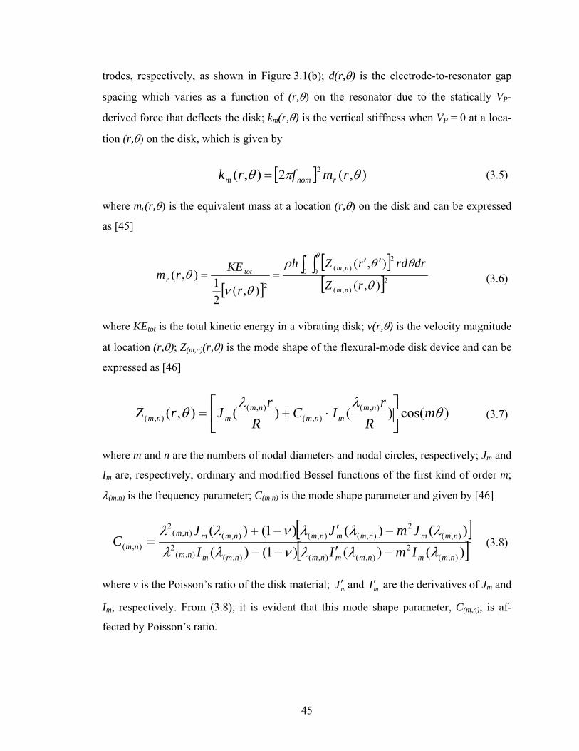
Figure 3.3: LCR equivalent circuit modal of the flexural-mode disk resonator of Figure 3.1.
So the equivalent mass at a location (r,θ) can be obtained by plugging (3.7) and (3.8)
into (3.6) and yields
[ ][ ]2
),(
0
2
0
2),(
),(
),(),(
θ
θθρθ
π
rZ
drdrrZhrm
nm
R
nm
r∫ ∫ ′′
= (3.9)
In this nickel flexural-mode disk case, m and n are equal to 2 and 0, respectively.
Then from [46], λ(2,0) is 2.31481 and C(2,0) is 0.21342 for Poisson’s ration v = 0.3, which
is close to the nickel’s Poisson’s ratio, 0.31.
3.3 Small-Signal Electrical Equivalent Circuit
To model and simulate the frequency characteristic of this disk resonator, an electri-
cal equivalent circuit is required, so Figure 3.3 presents this LCR equivalent circuit for
the flexural-mode disk resonator. The circuit elements and transformer ratios are derived
from the lumped mass, stiffness, damping, and voltage-to-force transfer function of the
flexural-mode disk, and can be expressed by
47
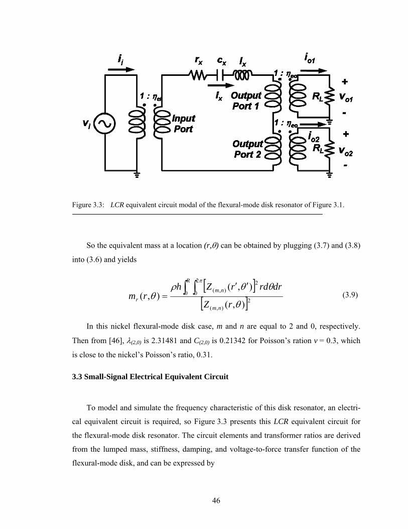
Figure 3.4: Simplified LCR equivalent circuit model presenting the real measurement setup of
the flexural mode disk resonator.
rerere
xre
xrex cQ
kmr
kcml ==== ,1, (3.10)
where mre, kre, and cre are the effective mass, stiffness, and damping, respectively, at the
highest velocity points, (R,π/4), (R,3π/4), (R,5π/4), and (R,7π/4) of the disk resonator.
In the equivalent circuit model of Figure 3.3, the transformer turn ratios for the input
and output ports can be given by the electromechanical coupling coefficients
[ ]2
12
),(
),(
),(),(),(),(
⎪⎭
⎪⎬⎫
⎪⎩
⎪⎨⎧
′′′′
′′=
∂∂
= ∫∫ ∫∫ θθθθε
θθ
ηrdrddrddrdk
rZrZ
VzCV reo
A Anm
nmPPe
in ini (3.11)
[ ]2
12
),(
),(
),(),(),(),(
⎪⎭
⎪⎬⎫
⎪⎩
⎪⎨⎧
′′′′
′′=
∂∂
= ∫∫ ∫∫ θθθθε
θθ
ηrdrddrddrdk
rZrZ
VzCV reo
A Anm
nmPPe
out outo (3.12)
As shown in Figure 3.1(b), there are two output electrodes with the identical electrode
area and this also reflects in Figure 3.3, showing two output ports with identical trans-
former turn ratio. For convenience, in the real measurement setup, usually these two out-
put electrodes are tied together via the wire bonding.
48
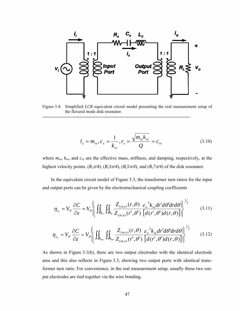
Figure 3.5: Final cross section of the nickel surface micromachining process for a flexural-mode
disk micromechanical resonator. The completed process flows are described in sec-tion 2.1.1 and 2.2.2.
To simplify the circuit of Figure 3.3 and reflect the real measurement setup of two
output electrodes wire-bonded together, Figure 3.4presents the simplified circuit with
only one output port and the transformer turn ratios are 1:1. The values of the model pa-
rameters in Figure 3.4 are given by
io
io
io ee
rex
re
eex
ee
rex
cRk
CmLηη
ηηηη 2
,2
,2
=== (3.13)
3.4 Experimental Results
The flexural-mode side-supported disk resonators were fabricated via the nickel sur-
face micromachining process described in section 2.1.1 and 2.2.2. Figure 3.5 presents the
final cross-section for the nickel flexural-mode disk resonator constructed in these proc-
esses. Figure 3.6 presents the global-view SEM of the flexural-mode disk resonator iden-
tifying key dimensions and this particular device was fabricated via the parylene-C sacri-
ficial layer process.
49
Figure 3.6: An SEM of a fabricated flexural-mode side-supported disk resonator.
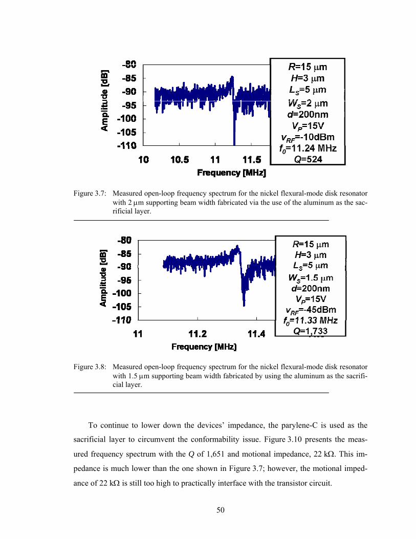
Figure 3.7 and Figure 3.8 present the measured frequency characteristics of the
nickel flexural-mode disk resonator with side-support beams of 2 μm and 1.5 μm width,
respectively, using the aluminum sacrificial layer process. These frequency spectra
clearly show that the smaller the width of the supporting beam the higher the Q of the
nickel disk resonator. The Q factor, 1,733, of the nickel flexural-mode disk resonator
with 1.5 μm supporting beam width is three times higher than that of 524 with 2 μm ver-
sion. However, the conformability issue of the sputtered aluminum really hinders these
devices from being able to interface with the transistor circuit due to their very high mo-
tional impedance. In this fabrication process, the 200 nm sputtered aluminum is used to
prevent the nickel structure making any contact with the electrodes underneath it but even
with 200 nm sacrificial layer thickness, the yield for the single disk resonator is still too
low. Moreover, for the flexural-mode disk-array resonator, not only the yield is not good
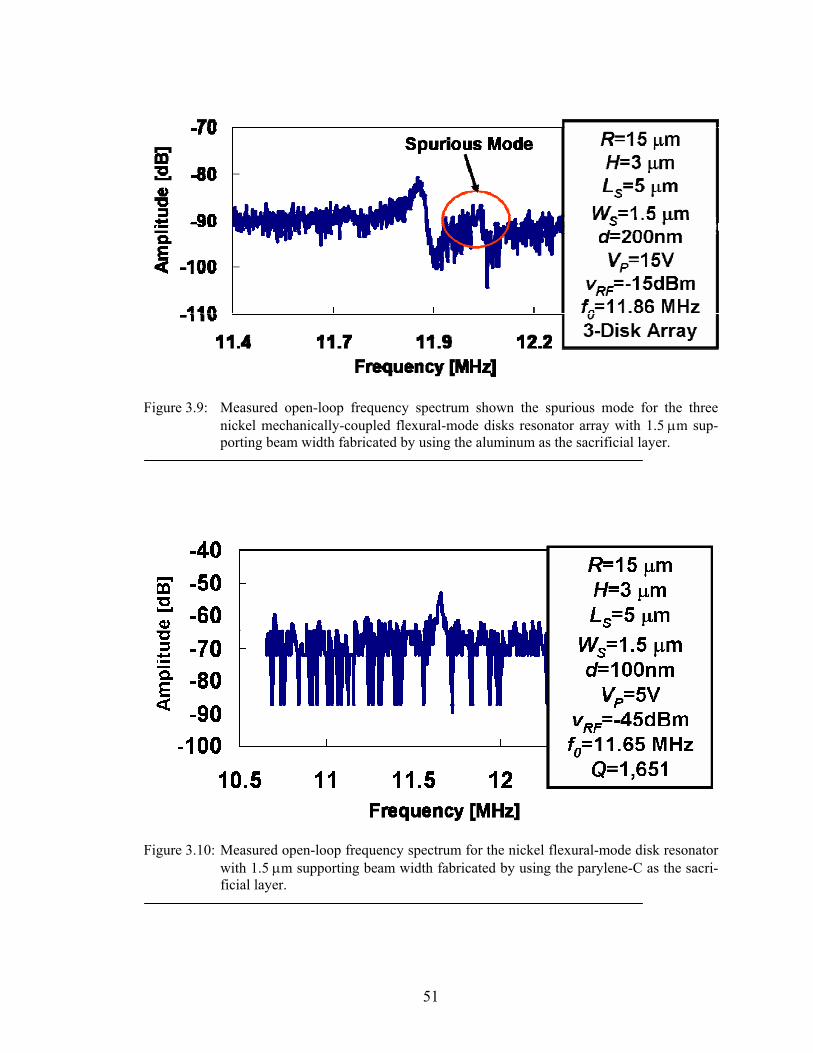
but also the spurious mode is introduced into the frequency spectrum, shown in
Figure 3.9, for the three-disk array resonator.
50
Figure 3.7: Measured open-loop frequency spectrum for the nickel flexural-mode disk resonator
with 2 μm supporting beam width fabricated via the use of the aluminum as the sac-rificial layer.
Figure 3.8: Measured open-loop frequency spectrum for the nickel flexural-mode disk resonator
with 1.5 μm supporting beam width fabricated by using the aluminum as the sacrifi-cial layer.
To continue to lower down the devices’ impedance, the parylene-C is used as the
sacrificial layer to circumvent the conformability issue. Figure 3.10 presents the meas-
ured frequency spectrum with the Q of 1,651 and motional impedance, 22 kΩ. This im-
pedance is much lower than the one shown in Figure 3.7; however, the motional imped-
ance of 22 kΩ is still too high to practically interface with the transistor circuit.
51
Figure 3.9: Measured open-loop frequency spectrum shown the spurious mode for the three
nickel mechanically-coupled flexural-mode disks resonator array with 1.5 μm sup-porting beam width fabricated by using the aluminum as the sacrificial layer.
Figure 3.10: Measured open-loop frequency spectrum for the nickel flexural-mode disk resonator
with 1.5 μm supporting beam width fabricated by using the parylene-C as the sacri-ficial layer.
52
Figure 3.11: Perspective view schematic of a micromechanical flexural-mode disk resonator ar-
ray, identifying key dimensions and showing a typical two-port bias and excitation configuration.
3.5 Mechanically Coupled Microresonator Array
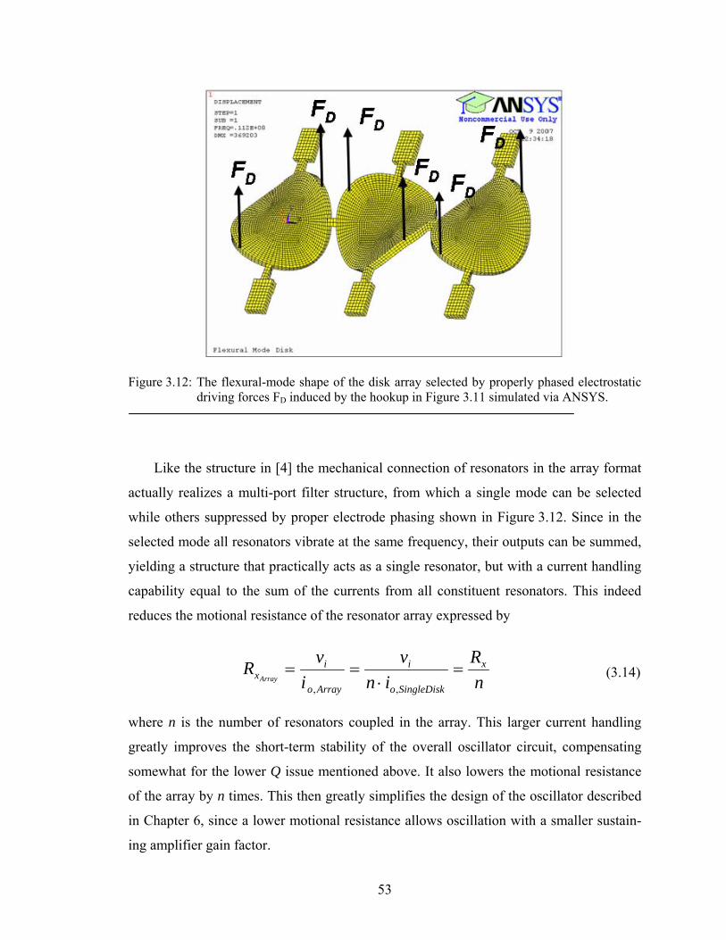
Figure 3.12 depicts the nickel flexural-mode disk resonator array connected in the
typical two-port bias scheme. Like the array of [4], this structure consists of several disk
resonators coupled by mechanical beams. Unlike the array of [4], which used the lateral
vibrating wine-glass mode resonators, the disks in the present array are designed to vi-
brate in the flexural mode used in [47]. Each disk has a radius of 15 μm and thickness of
3 μm, and is equipped with electrodes spaced d0 = 100 nm from the undersides of each of
its four quadrants that not only provide capacitive transduction, but also allow selection
of the resonator mode shape via proper phasing of signals applied to each quadrant.
53
Figure 3.12: The flexural-mode shape of the disk array selected by properly phased electrostatic
driving forces FD induced by the hookup in Figure 3.11 simulated via ANSYS.
Like the structure in [4] the mechanical connection of resonators in the array format
actually realizes a multi-port filter structure, from which a single mode can be selected
while others suppressed by proper electrode phasing shown in Figure 3.12. Since in the
selected mode all resonators vibrate at the same frequency, their outputs can be summed,
yielding a structure that practically acts as a single resonator, but with a current handling
capability equal to the sum of the currents from all constituent resonators. This indeed
reduces the motional resistance of the resonator array expressed by
nR
inv
ivR x
SingleDisko
i
Arrayo
ixArray
=⋅
==,,
(3.14)
where n is the number of resonators coupled in the array. This larger current handling
greatly improves the short-term stability of the overall oscillator circuit, compensating
somewhat for the lower Q issue mentioned above. It also lowers the motional resistance
of the array by n times. This then greatly simplifies the design of the oscillator described
in Chapter 6, since a lower motional resistance allows oscillation with a smaller sustain-
ing amplifier gain factor.
54
Figure 3.13: SEM’s of flexural-mode disk-array resonator using three of mechanically-coupled
disks.
Figure 3.14: SEM’s of flexural-mode disk-array resonator using nine of mechanically-coupled
disks.
3.6 Experimental Results
Figure 3.13 and Figure 3.14 presents SEM’s of fabricated nickel disk arrays, using
the fabrication process combined the nickel surface micromachining and CVD’ed pary-
lene-C deposition technology, with three and nine of coupled resonators. The measured
frequency spectra for a stand-alone disk resonator together with arrays using three and
nine mechanically coupled resonators are shown in Figure 3.15, where a rise in output
current with resonator number is clearly seen, and all Q’s are greater than 1,000. For the
nine resonators mechanically coupled array, the motional resistance is dramatically re-
55
Figure 3.15: Measured open-loop frequency characteristic for nickel mechanically-coupled flex-
ural-mode disk resonator arrays.
duced down to 5.8 kΩ, and now this level of motional resistance is suitable to interface
with transistor circuits. For fair comparison of motional resistances, all devices shared the
same 5V DC bias during measurement.
3.7 Spurious Responses
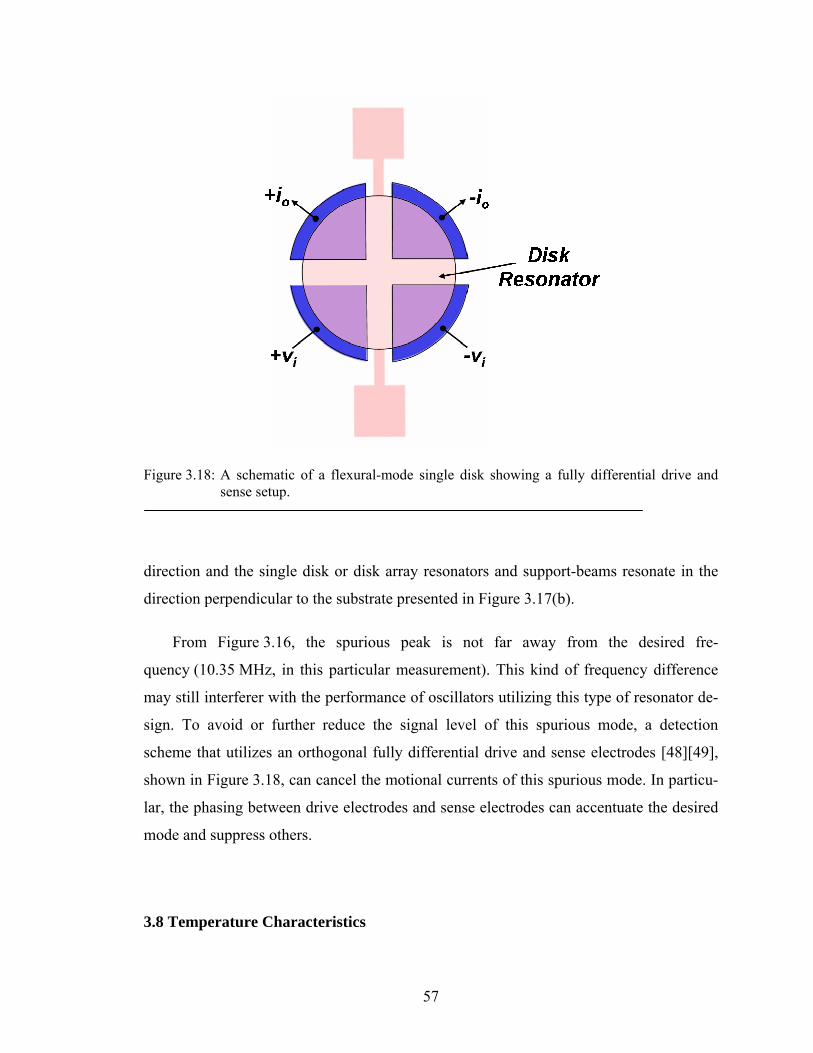
The nickel flexural-mode disk array resonator does have a significant drawback, spu-
rious modes from the lower frequency mode shape. Figure 3.16 presents the frequency
characteristic for a three nickel flexural-mode disk array resonator measured over a wide
frequency range, from 10 kHz to 20 MHz, in search of the spurious modes. Here, there is
no spurious modes around the designed mode, the first filter mode, however, in the lower
frequency range, at 2.75 MHz , the unwanted mode is observed. This unwanted mode
shape is simulated in ANSYS shown in Figure 3.17(a), the perspective-view of a three
resonators array. This is a trampoline mode, where the support beams all flex in the same
56
Figure 3.16: Measured frequency spectrum verifying no spurious modes around the desired mode
of the three nickel mechanically-coupled flexural-mode disks resonator array but the spurious mode is observed in low frequency range.
Figure 3.17: The lower frequency mode shape of the disk array simulated via ANSYS for (a) the
perspective-view and (b) the side-view of a three resonator array.
57
Figure 3.18: A schematic of a flexural-mode single disk showing a fully differential drive and
sense setup.
direction and the single disk or disk array resonators and support-beams resonate in the
direction perpendicular to the substrate presented in Figure 3.17(b).
From Figure 3.16, the spurious peak is not far away from the desired fre-
quency (10.35 MHz, in this particular measurement). This kind of frequency difference
may still interferer with the performance of oscillators utilizing this type of resonator de-
sign. To avoid or further reduce the signal level of this spurious mode, a detection
scheme that utilizes an orthogonal fully differential drive and sense electrodes [48][49],
shown in Figure 3.18, can cancel the motional currents of this spurious mode. In particu-
lar, the phasing between drive electrodes and sense electrodes can accentuate the desired
mode and suppress others.
3.8 Temperature Characteristics
58
Figure 3.19: Measured frequency versus temperature plots for nickel flexural-mode single disk
resonator and three disks resonator array.
To verify the fractional frequency temperature coefficient equation, MMR Tech-
nologies temperature control system was used for this experiment. Figure 3.19 presents
the measured plots of fractional frequency change versus temperature for a nickel flex-
ural-mode single disk and three disks array. The uncompensated temperature coefficients
extracted from the measured plots for a nickel flexural-mode single disk and three disks
array are -61.7 ppm/oC and -70.9 ppm/oC, respectively. Although these uncompensated
temperature coefficients for the nickel single disk resonator or three disks resonator array
are higher than the quartz crystal, polysilicon, single crystal silicon, and AlN, the frac-
tional frequency change versus the temperature relationships for the nickel single resona-
tor and three nickel disks array are linear over the temperature.
3.9 Conclusion
59
Nickel flexural-mode single disk resonators with the side-supported beams have
been demonstrated at frequency up to 11.6 MHz with the Q’s >1,000 and by using the
conformal and pin-hole free parylene-C as the sacrificial layer, the motional resistance
can be lowered down to 22 kΩ. The mechanically-coupled nickel resonator arrays have
been proved with motional resistances smaller than that of a single resonator by a factor
equal to the number of resonators used in the array. Especially, the motional resistance of
the nine nickel disks coupled resonator array has been improved to 5.8 kΩ, suitable to
integrate with the transistor circuits. This fully monolithic integration is described in
Chapter 6.
60
CHAPTER 4
NICKEL WINE-GLASS MODE DISK RESONATORS
Having described the HF micromechanical flexural-mode disk resonator array, its
resonant frequency is proportional and inversely proportional to the thickness and radius
of the disk, respectively. To increase the operating frequency, one can either increase the
thickness or reduce the radius. The issue of increasing the thickness is that the anchor loss
may become worse because of the vibration energy pumping through the anchor
vertically and the energy dissipating to the substrate, despite supporting at the nodal line.
And the drawback of reducing the disk radius is that it shrinks down the resonator-to-
electrode overlap area which eventually increases the motional resistance. This makes the
relatively high motional resistance of nickel flexural disk array compared to the quartz
crystal devices and makes it even harder to interface with other electronic circuits.
Pursuant to having resonators operating in VHF, a compound (2,1) mode disks, often
dubbed “wine-glass disks”, first introduced in [50], were designed to operate in the radial
mode instead of the flexural mode to reduce the anchor loss and boost the operating fre-
quency to VHF. The key for allowing the high-Q of these types of devices is the support
structures that better isolate the disks from their anchors. As described in [5] and [50], the
amount of isolation achieved is a strong function of (1) the size of the supporting center
stem; (2) whether or not a stem is even used; (3) the dimensions of any side supports; and
(4) the number and placement of side supports used. So in this Chapter, center stem and
stemless disks are demonstrated first and due to the resolution issue of the mask for this
particular run, side-supported disks are unable to test. But latter with the better resolution
mask from the commercial foundry, the side-supported devices are measurable. Again
both measurement results verify the theory of the support structures to preserve the high-
Q of nickel structural material.
61
RL
Input Electrode
Output Electrode
VP
Nitride Gap
iO
Vi
Disk
RH
A BVO
r
z
θ dO
RL
Input Electrode
Output Electrode
VP
Nitride Gap
iO
Vi
Disk
RH
A BA BVO
r
z
θr
z
θ dO
Figure 4.1: Perspective view schematic of a solid dielectric gap disk resonator identifying key
features and showing a two-port measurement scheme.
4.1 Resonator Structure and Operation
Figure 4.1 presents the perspective-view schematic of one of the wine-glass disk
resonators used in this work, connected to in its typical electrical bias, excitation, and
measurement scheme. As seen in the figure, the device is composed of a 3 μm-thick
nickel disk resonator suspended 400 nm above a ground plane by a stem placed at the
disk center and anchored to the substrate below. Four separate electrodes spaced less than
100 nm from the disk edges are placed on four different quadrants surrounding the disk to
specifically excite its compound (2,1) mode, which is shown in Figure 4.2. In practice,
the gaps between the resonator and its electrodes can be either air-filled or solid-filled,
with the latter the more preferable, since solid-filled gaps both reduce resonator imped-
ance and raise the fabrication yield of devices.
To operate this device, a dc bias VP is applied to the disk structure and an ac input
voltage vi is applied to one pair of opposing electrodes along the same axis (i.e., the input
62
Contorted Disk Shape
Original Disk Shape
Contorted Disk Shape
Original Disk Shape
Figure 4.2: Vibration mode shape for an 18 μm radius wineglass mode disk micromechanical
resonator obtained via ANSYS FEA.
axis). (Note that no current flows once the structure is charged to VP, so there is no dc
power consumption.) These voltages then collectively create a time-varying electrostatic
excitation force between the electrodes and the disk, in the lateral direction, and at the
frequency of the ac input voltage if VP>vi. When the AC input frequency matches the disk
resonance frequency, the resulting resonance electrostatic force drives the disk into reso-
nance vibration, which then generates resonance motion along the orthogonal output axis,
depicted in Figure 4.1. Motion along the output axis results in a dc biased time-varying
capacitance at the output electrodes, which produces an output current io given by
io
o
r
Poo
o
ooPPo v
dHR
kQVX
dAV
tCVi ⋅⋅=⋅⎟⎟
⎠
⎞⎜⎜⎝
⎛⋅≅⎟
⎠⎞
⎜⎝⎛
∂∂
= 4
22222
2
πεωωε (4.1)
where A0 = (πR)H, R, H, d0, kr and Q are the electrode-to-resonator overlap area, radius,
thickness, gap spacing, effective stiffness, and quality factor, respectively, of the disk
resonator; X is the amplitude of resonator vibration; ω0 = 2πf0 is the radian resonance fre-
63
quency; ε0 is the dielectric constant; and an approximate form for ∂C/∂t has been used.
The expression for resonance frequency has been presented below [51], as
( )[ ] ( )2nnqqnqn nn −=−−Ψ⋅⎥⎦
⎤⎢⎣
⎡−−⎟⎟
⎠
⎞⎜⎜⎝
⎛Ψ ς
ξς (4.2)
where
( ) ( )( )
( )
21
2
222
22
0
2
2
1
=−
=
+=
−=
=Ψ −
n
ERf
nq
xJxxJ
xn
nn
σξ
σρπς
ς
(4.3)
and where Jn(x) is the Bessel function of first kind of order n; f0 is the resonance
frequency; and ρ, σ and E, are the density, Poisson ratio, and Young’s modulus,
respectively, of the disk structural material.
Figure 4.3: Top-view illustration of the wine-glass mode disk resonator with polar coordination
showing the tangential and radial directions at the point (r,θ).
64
Figure 4.4: Normalized polar plot of radial and tangential displacements of the wine-glass disk
vibration mode shape.
4.2 Design for Support Structures
Figure 4.3 presents the schematics of disk and electrodes configuration in a polar co-
ordination with variables for wine-glass mode disk vibration. The relative radial, U(r,θ),
and tangential displacements, V(r,θ), at any given point (r,θ) on the disk as depicted in
Figure 4.4 can be expressed as
θζξζθ n
RrJ
rABn
RrJ
rrU nn cos1),( ⋅⎥
⎦
⎤⎢⎣
⎡⎟⎠⎞
⎜⎝⎛+⎟⎟
⎠
⎞⎜⎜⎝
⎛∂∂
= (4.4)
θζξζθ n
RrJ
rAB
RrJ
rnrV nn sin),( ⋅⎥
⎦
⎤⎢⎣
⎡⎟⎠⎞
⎜⎝⎛
∂∂
+⎟⎟⎠
⎞⎜⎜⎝
⎛−= (4.5)
where
[ ])1()(2
)1(2)(2 2
+−Ψ
+−+Ψ=
nn
nn
AB
n
n
ζ
ζξζ
(4.6)
65
B/A = -4.5236 when n = 2. The radial and tangential displacements showing in (4.4) and
(4.5) do not represent the real amount of displacements. However, plotting (4.4) and (4.5)
together in the same normalized polar coordinate shown in Figure 4.4, did help to under-
stand the relative magnitudes between the radial and tangential displacements. Compar-
ing the maximum radial and tangential displacements at 0° and at 45°, respectively, the
factor is 2.5. So unlike the radial contour mode disk, which only has aerial dilation, the
wine-glass mode disk exhibits both aerial as well as rotation, yielding a compound mode
shape with nodal points on the disk perimeter, and at the center of the disk. The wine-
glass mode shape allows for more flexibility in anchoring this structure compared with
the radial contour mode, hence, more degree of freedom to suppressing anchor-associated
energy losses.
This wine-glass disk design is quite suitable for anchor loss evaluation, since, as
shown in [50][52] the amount of anchor loss experienced by this particular design can be
specified by selection of the anchor type (i.e., center stem or side support), the number of
anchors, and the geometry of the anchors (i.e., stem size). So in this work, not only the
center stem is designed, fabricated, and tested but also the side-supported beams are util-
ized to minimize the anchor loss mechanism and preserve the high-Q of nickel microme-
chanical resonators.
From Figure 4.4, the center portion of the disk is motionless therefore for the center
stem designs, the stem sizes vary from stemless to 2 μm in radius. For the side-support
design, the support attachment points, 45°, 135°, 225°, and 315°, are so called quasi-nodal
points, no radial displacement but small tangential displacement. To isolate this tangen-
tial displacement energy loss through anchors to substrates, the side-supported beams
have to be designed to vibrate in a clamped-free flexural mode at the resonant frequency
of the wine-glass mode disks and their lengths are equal to the quarter-wavelength of the
wine-glass mode disk [50][53]. From the mechanical vibrational impedance perspective,
this quarter-wavelength supporting beam design transfers almost zero mechanical vibra-
tional impedance at the disk attachment points to the infinite mechanical vibrational im-
pedance at the anchor point. This allows the vibration energy from the tangential dis-
placement of the vibrating disk traveling through the supporting beam and reflects the
66
energy back to the disk once it hits the infinite impedance at the anchor points to maxi-
mum Q. The length of the support beam Ls to achieve the quarter-wavelength design is
expressed by
ρπλ E
fWL si
s0
22
34= (4.7)
where λi=1.8751047, and Ws is the width of the support beam.
4.3 Measurement Techniques
Test and measurement of resonators is one of the challenging aspects of this work
due to incomplete electrode-to-resonator overlap described in Chapter 2 because this
greatly reduces the driving and sensing area as a result of reduction of the output current
from the resonator. Factors that may cause this include: parasitic feedthrough, improper
resonator design or inadequate clean room facilities. The signal level can be reduced to a
point that the motional current is very difficult to detect. Several different measurement
techniques are used in this work to overcome these challenges and to extract the real
device performance.
4.3.1 Mixing Measurement Setup
As mentioned in the previous chapter, the incomplete electrode-to-resonator overlap
leads to the high motional resistance and the weak motional current. In order to dig out
this weak signal buried in the noise floor of the frequency spectrum and preserve true
mechanical Q values of devices, the mixing measurement technique has to be used to
suppress the parasitic feedthrough current by moving the motional current of the resona-
67
MechanicalSignal Input
ωLO
ωLO
ω
ω
ωo=ωLO - ωRFElectricalSignal Input
ωRF
ωRF
ResonatorResponse
ω o
MotionNo
Motion
No Motion
(Force)
MechanicalSignal InputMechanicalSignal Input
ωLO
ωLO
ω
ω
ωo=ωLO - ωRFωo=ωLO - ωRFElectricalSignal Input
ElectricalSignal Input
ωRFωRF
ωRFωRF
ResonatorResponseResonatorResponse
ω oω o
MotionMotionNo
Motion
No Motion No
Motion
No Motion
(Force)
Figure 4.5: Electrical and mechanical signal plots illustrating conversion of off-resonance elec-
trical signals at wLO and wRF down to a force at wIF.
tor away from them in the frequency domain. As depicted in Figure 4.5 and described
more detail in [7], a capacitive electromechanical resonator uses the square-law voltage-
to-force transfer function of its transducer to mix two signals and generates a mechanical
force at the IF frequency. Then the parasitic current will be greatly reduced in the IF fre-
quency range to allow the detectable motional current.
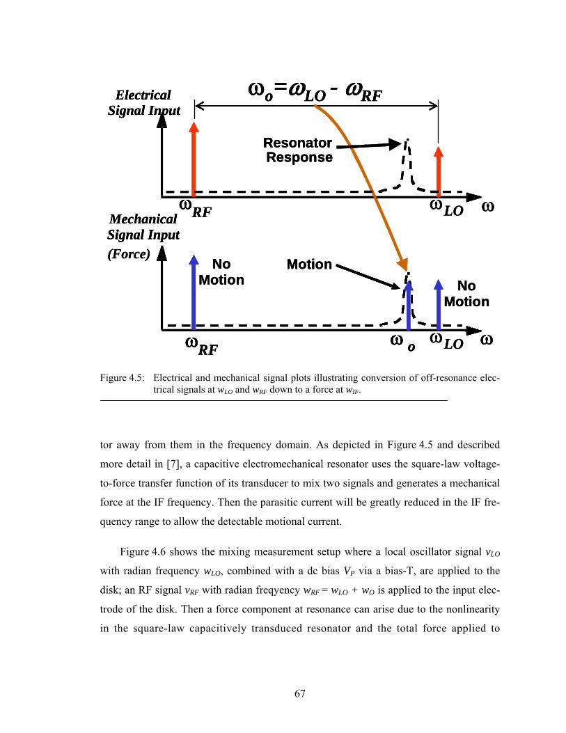
Figure 4.6 shows the mixing measurement setup where a local oscillator signal vLO
with radian frequency wLO, combined with a dc bias VP via a bias-T, are applied to the
disk; an RF signal vRF with radian freqyency wRF = wLO + wO is applied to the input elec-
trode of the disk. Then a force component at resonance can arise due to the nonlinearity
in the square-law capacitively transduced resonator and the total force applied to
where the mixed component of interest Fmix at resonant frequency has been singled out in
the last formula. This in-band force drives the disk resonator into vibration and the tested
resonator produces an output current tracing out a high Q bandpass biquad frequency
characteristic and fed into a spectrum analyzer in MAX HOLD mode, which records its
highest value as the RF signal is swept within a frequency span.
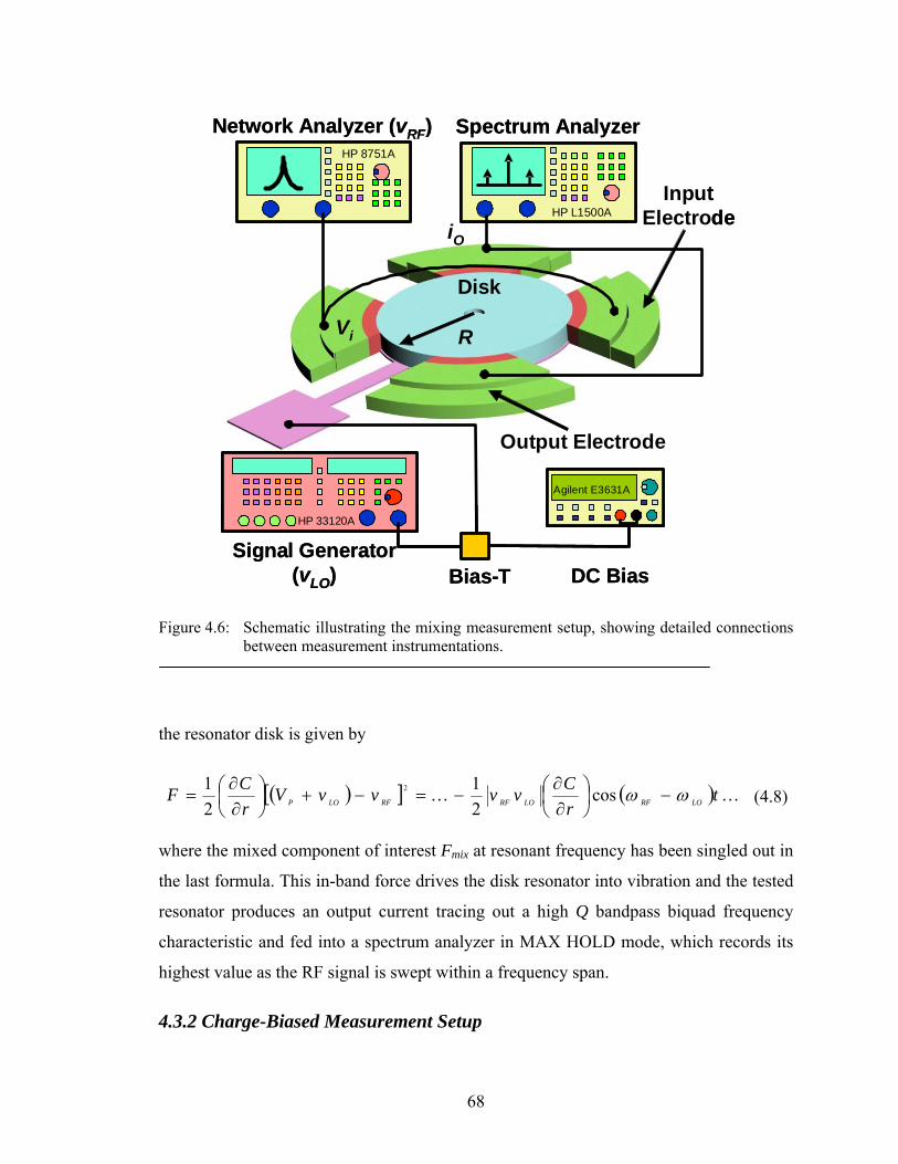
4.3.2 Charge-Biased Measurement Setup
69
In the laboratory, testing of charge-biased resonators was done via the procedure
summarized in Figure 4.7. Here, all electrodes surrounding the disk resonator are first
grounded; then a dc bias voltage Vcharge is applied to the electrode underneath the disk
structure. Next, a probe tip biased to Vcharge is gently touched to the side wall of the con-
ductive disk structure, charging it to Vcharge. Upon pulling the probe tip away from the
disk, the charge remains on the structure for a time governed by its leakage rate, which
from [54], has a time constant on the order of 40 minutes—plenty long enough to take
several high resolution measurement sweeps. Upon charging the resonator, the printed
circuit board on which the resonator die is mounted is then transferred from the probe
station into the custom built vacuum chamber and hooked up to the electrical
feedthroughs. Mixing measurement [55] then proceeds as usual, except that the local os-
cillator and RF signals must now be combined at the input, rather than added to the dc-
bias port of previous renditions.
4.5 Experimental Results
Disk devices were fabricated using the process flow described in Chapter 2, then
tested in a custom-built chamber that could be pumped down to pressures below 50 μTorr.
Pressures this low were needed to eliminate the influence of viscous gas damping on the
Q’s of the resonator devices [56], thereby eliminating gas damping as a mechanism for
Q-limiting, and hence, better elucidating other loss mechanisms. For testing, each die
containing many resonator devices was mounted on a printed circuit board that was then
placed into the test chamber. Individual devices were accessed by bond wiring to metal
traces on the board, and air-tight electrical feedthroughs into and out of the vacuum
chamber provided both dc and coaxial electrical interconnections between the board and
external measurement instrumentation.
70
VVChargeCharge
Floating Floating DiskDisk
ProbeProbe
VVChargeChargeInput Input
ElectrodeElectrode
Output ElectrodeOutput Electrode
Input Input ElectrodeElectrodeVVChargeCharge
vvLOLO + + vvRFRF
iiOORRLL
vvOO
Output ElectrodeOutput Electrode
VVChargeCharge
Floating Floating DiskDisk
ProbeProbe
VVChargeChargeInput Input
ElectrodeElectrode
Output ElectrodeOutput Electrode
Input Input ElectrodeElectrodeVVChargeCharge
vvLOLO + + vvRFRF
iiOORRLL
vvOO
iiOORRLL
vvOO
Output ElectrodeOutput Electrode
Figure 4.7: Depictions of the hook-up procedure for charge-biased measurement. (a) Charge-
biasing the disk structure via a charged probe tip. (b) Electrical hook-up for mixing measurement of a charge-biased resonator.
(a)
(b)
71
-112
-107
-102
-97
-92
6.5 6.55 6.6 6.65 6.7 6.75
Frequency [MHz]
Pow
er [d
Bm
]Data:
Lr=40 μmWr=8 μmH=3 μm
do=400 nmVP=50V
VLO=6.25VVRF=3.56Vfo=6.62 MHz
Q=576
8 μm3 μm
40 μm
Input Electrode CC-BeamAnchorAnchor
-112
-107
-102
-97
-92
6.5 6.55 6.6 6.65 6.7 6.75
Frequency [MHz]
Pow
er [d
Bm
]Data:
Lr=40 μmWr=8 μmH=3 μm
do=400 nmVP=50V
VLO=6.25VVRF=3.56Vfo=6.62 MHz
Q=576
8 μm3 μm
40 μm
Input Electrode CC-BeamAnchorAnchor
Figure 4.8: (a) SEM and (b) measured frequency characteristic for a 6.6-MHz vertically actuated
clamped-clamped beam resonator measured using the mixing measurement technique.
4.5.1 Nickel CC-Beam
In addition to wine-glass disks, CC-beam resonators were also included in the proc-
ess run in order to gauge the material quality of present fabrication run versus ones that
had been run previously [45]. Figure 4.8(a) and (b) present the SEM and measured fre-
quency characteristic, respectively, for a 40 μm-long, 8 μm-wide, 3 μm-thick vertically
resonant CC-beam micromechanical nickel resonator achieved in this run. Because the
400 nm vertical electrode-to-resonator gap achieved by the present process (which is not
optimized for vertical CC-beam resonators) is much smaller than the usual 100 nm used
for such devices, this device has a much weaker capacitive transducer than previous CC-
beams, so its motional output currents are substantially smaller. To isolate the device’s
tiny motional current from feedthrough parasitic currents that might otherwise mask it,
the mixing measurement scheme of [55] was used to detect and plot the device response,
shown in Figure 4.8(b). Because the mixing measurement method of [55] is used, the
(a)
(b)
72
units of the y-axis of Figure 4.8(b) are not dB’s, but rather power dBm’s, as measured by
a spectrum analyzer in MAX HOLD mode [55]. In addition, the very low dBm levels
seen in the data (and in data to follow) are caused by the impedance mismatch between
the kΩ resonators and the 50Ω input of the spectrum analyzer, and are not indicative of
actual device loss. The Q of the device gives a more accurate indication of its loss in a
matched circuit application (e.g., in a filter).
From the measured response, the Q of this device is only 576 at 6.62 MHz. This is
considerably lower than the 6,000-8,000 posted by previous 8.51-MHz polysilicon CC-
beam resonators [45]. Without careful consideration, one might conclude from this result
that nickel material has a lower intrinsic Q than polysilicon at HF to VHF frequencies.
Such a conclusion, however, would only be valid if the anchor losses known to dominate
the Q’s of polysilicon CC-beams were identical to those in the nickel ones. This might in
fact not be the case, since there is evidence that the attachment of nickel resonators to the
substrate at their anchors might not be as sturdy as their polysilicon counterparts. In par-
ticular, poor adhesion caused by the stress of the plated film between the structure and the
substrate might result in a weak anchor that ultimately dissipates more energy during vi-
bration. Thus, it is difficult to make any conclusions regarding loss mechanisms based on
CC-beam measurements.
4.5.2 Nickel Wine-Glass Disks With Stems
The anchor loss uncertainties posed by the above CC-beam device are not shared by
the wine-glass disk resonators of this work, since the latter possess supports structures
that better isolate the disks from their anchors. As described [50] and [52], the amount of
isolation achieved is a strong function of (1) the size of the supporting center stem; (2)
whether or not a stem is even used; (3) the dimensions of any side supports; and (4) the
number and placement of side supports used. Due to lithography issues during the fabri-
cation run, the side-supported devices of this work were not testable, and only stem-
supported devices were available for testing. In addition, due to the incomplete electrode-
73
Figure 4.9: Frequency characteristic of a 60-MHz wine-glass mode nickel disk supported by a
2 μm-radius center stem anchor measured using the mixing measurement technique.
to-resonator overlap described in Chapter 2, the mixing measurement scheme of [55] was
again required for measurement of disk devices.
Since the anchor dissipation of previous stem-supported disk resonators was found to
be a strong function of stem radius [17], insights into the impact of anchor losses on
nickel resonator Q can be obtained by merely measuring devices with different stem radii.
Pursuant to this, Figure 4.9 presents the measured frequency characteristic for an 18 μm-
radius nickel wine-glass disk with a rather large 2 μm-radius center stem, showing a Q of
only 490 at 60 MHz. This measurement was repeated over more than ten resonators with
this stem size, with all devices exhibiting Q’s under 500. Assuming a nickel density equal
to the bulk value of 8.9 kg/m3, the 60 MHz frequency of this device implies a Young’s
modulus of 195 GPa and acoustic velocity of 4,678 m/s for the plated nickel material of
this work.
74
Figure 4.10: Frequency characteristic of a 60-MHz wine-glass mode nickel disk supported by a
1.5 μm-radius center stem anchor measured using the mixing measurement tech-nique.
Next, a 1.5 μm-radius center stem wine-glass disk resonator was tested. Figure 4.10
presents the measured frequency characteristic, which again shows resonance at 60 MHz,
but this time with a Q in excess of 5,077. Clearly, the size of the center stem is a domi-
nant factor governing the Q of a nickel wine-glass disk. If so, then the maximum Q of
such a disk should ensue if the center stem can be eliminated. As mentioned, the side-
supported devices, which were devoid of center stems, were not functional due to fabrica-
tion issues in this particular run; so stemless side-supported devices were not available.
4.5.3 Stemless Nickel Wine-Glass Disks
Fortunately, there were devices on this run that had neither stems, nor side supports.
These devices were designed to be supported only by the solid material in their electrode-
to-resonator gaps. Such a device, however, poses some measurement difficulty, since it
75
Figure 4.11: Frequency characteristic of a stemless charge-biased 60-MHz wine-glass mode
nickel disk measured via the mixing measurement technique.
does not have a lead with which to apply a dc-bias VP to its conductive disk structure.
Fortunately, such a lead is not needed, since charge biasing can be used [54], where
charge is deposited onto the resonator structure using a probe. From [54], the discharge
time for a charge-biased resonator can be quite long, on the order of 900s before the out-
put signal for a stand-alone resonator is attenuated by 3dB.
Using this procedure, Figure 4.11 presents the measured frequency characteristic for
an 18 μm-radius 60 MHz nickel disk with no center stem support, suspended only by the
nitride material in the electrode-to-resonator gap. As shown, the disk exhibits a measured
Q of 54,507, which clearly exposes the enormous impact of the stem on nickel resonator
Q, and suggests that the nickel material quality is on par with other popular micromachi-
nable materials (e.g., polysilicon, polydiamond) from a Q perspective. In fact, to our
knowledge, the vacuum frequency-Q product of 3.3×10¹² attained by this particular
nickel resonator is the highest yet seen for any micro-scale metal resonator in the VHF
range.
76
-115
-113
-111
-109
-107
-105
-103
-101
0 100 200 300Res
onan
t Pea
k H
eigh
t [dB
m]
Elapsed Time [min]
3 dB attenuation at ~30min
-115
-113
-111
-109
-107
-105
-103
-101
0 100 200 300Res
onan
t Pea
k H
eigh
t [dB
m]
Elapsed Time [min]
3 dB attenuation at ~30min
Figure 4.12: Plot of resonance output amplitude versus discharging time for a charged-biased
micromechanical nickel disk resonator.
The use of charge biasing in the last experiment is intriguing, but begs the question:
How long before leakage currents discharge the effective charge-bias to the point of no-
ticeable performance degradation? To answer this, Figure 4.12 presents a measured plot
of resonant peak height versus time. As shown in the figure, leaky discharging of the
resonant structure in vacuum attenuates the output signal by 3 dB after 30 minutes, which
is plenty long enough to make measurements, and long enough to allow charge refreshing
via a very simple, low-power circuit.
4.5.4 Side-Supported Nickel Wine-Glass Disks
Latter the new mask set for the side-supported nickel wine-glass disk resonators is
from the commercial mask company instead of homemade from the Michigan Nanofabri-
cation Facility, so the resolution can really reduce down to 1 μm. As shown in
Figure 4.13, to operate this side-supported disk, a local oscillator signal vLO, combined
77
Figure 4.13: Perspective view schematic of a solid dielectric gap side-supported disk resonator
identifying key features and showing a mixing measurement scheme.
with a dc bias VP , is applied to the disk through the anchor and supporting beam. This is
the only difference in operation compared to the center stem disk resonator described in
section 4.5.1.
Since the anchor dissipation of previous side-supported disk resonators [52] was
found to be a strong function of the width of the supporting beam, through different sup-
porting beam widths measurement, the impact of such anchor losses on nickel resonator
Q can be obtained. Pursuant to this, Figure 4.14(a) and (b) present the globe view of the
fabricated device and the zoom in view of the supporting beam SEMs indicating the 2 μm
supporting beam width, respectively. Figure 4.14(c) shows the measured frequency char-
acteristic for a nickel wine-glass disk with a 2 μm supporting beam width, showing a Q
of 2,458 at 62.6 MHz.
78
Figure 4.14: (a) Globe view and (b) zoom-in view SEMs of a 62-MHz side-supported wine-glass
mode nickel disk with 2 μm supporting beam width and (c) frequency characteristic of this device measured using the mixing measurement technique.
Next, a 1.8 μm supporting beam width wine-glass disk resonator was under test.
Figure 4.15(a) and (b) show the global view SEM of the fabricated device and the zoom
in view of the supporting beam indicating the 1.8 μm supporting beam width, respec-
tively. Figure 4.15(c) shows the measured frequency characteristic for a nickel wine-glass
disk with a 1.8 μm supporting beam width, showing a Q of 5,385 at 62.2 MHz. Obvi-
ously, the size of the supporting width is the key factor governing the Q of a nickel side-
supported wine-glass disk resonator.
Finally the side-supported wine-glass disk resonator with 1 μm supporting beam
width was fabricated and tested. The fabricated results are presented in Figure 4.16(a)
and (b) for the global-view and supporting beam zoom-in SEMs, respectively. The
(a) (b)
(c)
79
Figure 4.15: (a) Globe view and (b) zoom-in view SEMs of a 62-MHz side-supported wine-glass
mode nickel disk with 1.8 μm supporting beam width and (c) frequency characteris-tic of this device measured using the mixing measurement technique.
measured frequency characteristic for a nickel wine-glass disk with a 1 μm supporting
beam width shows the Q of 22,949 in Figure 4.16(c). This result once again suggested
that the nickel material quality is on par with other popular micromachinable materials
from a Q perspective. Compared this result with the stemless wine-glass disk resonator,
the Q is around one half of that of the stemless counterpart but the measurement method
for the side-supported disk resonator is much easier in the laboratory.
4.6 Conclusions
Wine-glass nickel micromechanical disk resonators with nitride dielectric capacitive
(a) (b)
(c)
80
Figure 4.16: (a) Globe view and (b) zoom-in view SEMs of a 62-MHz side-supported wine-glass
mode nickel disk with 1 μm supporting beam width and (c) frequency characteristic of this device measured using the mixing measurement technique.
transducer gaps have been demonstrated with frequency-Q products as high as 3.3×10¹²,
which is the highest to date for any micro-scale metal resonator device in the VHF range.
This result proves that the intrinsic Q limit of plated nickel thin-films is more than ade-
quate for VHF filtering and oscillator applications, and on par with that of other popular
micromachinable materials, including polysilicon [57]. The above characteristics, com-
bined with the only 50oC plating temperature required for its deposition, makes nickel a
very strong candidate for use in modular MEMS-transistor merging processes seeking to
integrate MEMS over finished foundry transistors in a fully monolithic, post-transistor
fashion.
(a) (b)
(c)
81
CHAPTER 5
NICKEL MICROMECHANICAL SPOKE-SUPPORTED RING RESONATORS
A micromechanical vibrating spoke-supported ring resonator fabricated in a low
deposition temperature nickel metal material has been demonstrated in two vibration
modes spanning frequencies from HF (18 MHz) to UHF (425.7 MHz) with Q’s as high as
6,405 and 2,467, respectively. The use of an anchor isolating spoke-supported ring
geometry along with notched support attachments between the ring structure and
supporting beams contributes to demonstration of the highest reported vibrating
frequency to date for any macro or micro-scale metal resonator in the UHF range, making
this the first metal micromechanical resonator suitable for RF filtering and oscillator
applications. Because the nickel structural material is deposited at 50oC, the fabrication
process for this resonator is quite amenable to post-processing over finished foundry
CMOS wafers, even ones with gate lengths below 65 nm slated to use advanced low-k
(but low melting point from 300-400oC) dielectric material around their metals. This
makes nickel structural material an attractive choice for low cost post-transistor single-
chip integration of high Q vibrating passives with transistor circuits for wireless
applications. 5.1 Resonator Structure and Operation
Figure 5.1 presents a perspective view schematic of the ring resonator design, identi-
fying key dimensions and indicating a two-port bias and excitation scheme. The device is
similar to that of [18] and comprises a 3 μm-thick nickel ring resonator suspended
400 nm above a ground plane by four spokes centrally anchored to an underlying ground
plane. Eight electrodes are placed at four quadrants overlapping the inside and outside of
82
Figure 5.1: Perspective view schematic of a micromechanical spoke-supported ring resonator,
identifying key dimensions and showing a typical two-port bias and excitation con-figuration.
the ring so as to specifically excite the ring into one of the two contour mode shapes,
shown in Figure 5.2.
To operate this device in its two-port configuration shown in Figure 5.1, a dc-bias
voltage, Vp is applied to the ring structure and an ac signal vi to its inner electrodes, creat-
ing an time varying electrostatic force acting radically on the ring. When the input signal
are acting at the resonant frequency of the device, that force is multiplied by the Q factor
of the resonator, resulting expansion and contraction of the ring around its CAD-defined
width along its inner and outer perimeters like the anti-symmetric mode shape of
Figure 5.2(b). This vibrating motion results in a time-vary, dc-biased capacitor between
the ring and the output electrodes generating an output current io. This current is corre-
sponding to the vibrational resonance frequency of the ring governed by its material
properties and its width. The use of non-intrusive, centrally-anchored spoke-supported
forces the length of the support beam Ls must be designed first and corresponded to one
or more quarter-wavelengths at the desired frequency f0 by the expression
83
Figure 5.2: Finite element simulated (a) 1st contour mode (symmetric mode) and (b) 2nd contour mode shape (anti-symmetric mode) for the nickel ring resonator of Figure 5.1.
...5,3,1,4 0
=⋅
⋅= af
E
aLSρ
(5.1)
where E and ρ are the Young’s modulus and density of the structural material,
respectively, and a is the odd number corresponding to different quarter-wavelengths.
Then Ls determines the inner radius of the ring ri and outer radius ro and can be solved by
the expression of
Efh )1(2
2
0σρπ −
= (5.2)
and
[ ] [ ][ ] [ ] 0)()()()()()(
)()()()()()(
011011
011011
=+−×+−−+−×+−
ooooiiii
ooooiiii
hrhJrhrJhrJhrhYrhrYhrYhrhYrhrYhrYhrhJrhrJhrJ
σσσσ
(5.3)
84
where Ls, ri, and ro are identifying in Figure 5.1; σ is the Poisson ratio of the structural
material; and Jx and Yx are Bessel functions of the first and second kinds, respectively.
This resonant frequency equations for the first and second modes can be simplified down
to
( ) Errf
oiapprox
ρ+
≈2
.0 (5.4)
and
( ) Errf
ioapprox
ρ−
≈2
.0 (5.5)
,respectively.
From [58], the presence of a solid dielectric-filled gap between a lateral resonator
and its electrodes does not necessarily constitute a dominating loss mechanism that dic-
tates Q. The wine-glass device of [58] in fact achieved Q’s in excess of 35,000, despite
its use of solid gaps. Thus, for the present ring resonator design, one might initially as-
sume that losses contributed by its solid-gap resonator-to-electrode interface are impor-
tant only if the Q of the overall resonator is on the order of 35,000. From [58], this is not
the case even for UHF rings constructed of polysilicon.
5.2 Nodal Circle Attachment
Thus, even with solid-gap capacitive transducers, given that anchor losses generally
dominate the Q’s of previous air-gap UHF resonators, the use of lossless anchor design
for the present nickel ring resonator is still important and beneficial. The design of
Figure 5.1 thus features the isolating spoke-support design first detailed in [18], where
the spokes are dimensioned to correspond to a quarter-wavelength at the ring’s resonance
frequency, and where notches are used to better access the extensional contour mode
nodal circle, like that of Figure 5.2(b).
85
Figure 5.3: Finite element simulated mode shape for a nickel ring resonator and arrows relating
points on a relative vibration displacement curve with locations on the ring.
The key to attaining high Q at UHF frequency in nickel material is to minimize an-
chor losses. In the overall structure, the use of a centrally-located anchor with longitudi-
nal-mode, quarter-wavelength, radial support beams provides a degree balance and isola-
tion that greatly suppresses anchor losses to the substrate. In the effort of further mini-
mizing anchor losses, the location of the support beam attachment to the ring structure is
designed to attach to the ring’s nodal circle. From the finite element simulated mode
shape of the ring, the relative vibration displacement at the nodal circle is the smallest in
the whole ring structure and from the theory, there should be no displacement at the nodal
circle, shown in Figure 5.3. In theory, if the support beam is attached to the nodal circle
location, once the ring structure starts to vibrate, the vibration energy should preserve in-
side the ring instead of passing to the supporting beam and losing to the anchor.
However, due to the lithography tolerance, the nodal circle attachment location may
not exactly match the designed value after the fabrication, this attempt should further
reduce the vibration energy of the ring structure transmitted to the supporting beam and
lost
86
Figure 5.4: Final cross-section for the nickel ring resonator constructed in this process.
to the substrate later on. To access the nodal circle locations, basically it cuts notches into
the ring structure, where the vibration frequency of the ring shifts from its designed value.
This will clearly be seen in the experimental results that only the ring structure utilizing
the notches at the support attachment locations can be measured in the UHF with Q’s
greater than 1,000.
5.3 Experimental Results
The ring resonators in this work were fabricated via a lateral solid-gap transducer
nickel plating process, similar to that reported in [37] for previous nickel wine-glass
mode disk resonators, except this time using SPR220-3.0 as the structure plating mold,
instead of AZ9260, in an effort to achieve the 1.5μm support beam features needed to
attain Q’s in the thousands. In this process, the temperature during nickel electroplating is
50oC, and the highest temperature step is 380oC for the PECVD silicon nitride gap mate-
rial, which can be lowered via use of atomic layer deposition (ALD), or some other lower
temperature dielectric deposition process. Figure 5.4 presents the final cross-section for
the nickel ring resonator constructed in this process, taken along the AA plane of
Figure 5.1.
87
Figure 5.5: Global-view SEM of the ring resonator and a zoom-in SEM on one of its direct sup-
port attachment locations.
Figure 5.5 presents the global-view SEM of the ring resonator with an anchor at the
center and a zoom-in SEM on one of its direct support attachment locations. Figure 5.6
shows the SEM of a notched version of the ring resonator. Despite the use of a slower
electroplating rate during electrode formation, the electrodes for the ring devices of this
work still exhibited the same undercutting near the ring sidewalls seen in [37], and shown
in Figure 5.7. The resultant incomplete electrode-to-resonator overlap raised the motional
impedances of the rings to several hundred kΩ’s, which made direct two-port measure-
ment of the devices quite difficult, since the expected motional current ends up being
smaller than feedthrough currents at UHF. To circumvent this problem, a mixing meas-
urement technique [17] was used to test the nickel rings. Briefly, mixing suppresses the
impact of feedthrough currents by moving them away from motional currents in the fre-
quency domain.
88
Figure 5.6: Global-view SEM of the ring resonator and a zoom-in SEM on one of its notched
support attachment locations.
Figure 5.7: Gap-zoomed SEM of the incomplete electrode-to resonator overlap.
89
Figure 5.8: Frequency characteristic of a fabricated nickel ring resonator with direct support
attachments operated at its first radial contour mode centered at 20.2 MHz, meas-ured via a mixing measurement technique.
Figure 5.9: Frequency characteristic of a fabricated nickel ring resonator with notched support
attachments operated at its first radial contour mode centered at 18 MHz, measured via a mixing measurement technique.
Figure 5.8 presents the measured frequency spectrum for the first contour mode of a
ring resonator with direct-support attachments (as opposed to notched support), centered
at 20.2 MHz with a measured Q of 1,154. Next, a ring resonator with notched support
90
Figure 5.10: Frequency characteristic of a fabricated nickel ring resonator with notched support
attachments operated at its second radial contour mode centered at 425.7 MHz, measured via a mixing measurement technique
attachment was tested. Figure 5.9 presents the measured frequency characteristic for its
first contour mode, showing a much higher Q of 6,405 at 18 MHz, verifying that careful
support design is still beneficial even when solid-gap capacitive transducers are utilized.
Finally, Figure 5.10 presents the measured frequency characteristic of this ring’s
second radial contour mode, vibrating at 425.7 MHz with a Q of 2,467, which is on par
with some polysilicon ring resonators [57], and which verifies that nickel could be every
bit as good as polysilicon in attaining high Q at high frequency.
5.4 Conclusions
In achieving a Q of 2,467 at 425.7 MHz, the nickel spoke-supported micromechani-
cal ring resonator attains the highest frequency reported to date for any micro-scale metal
resonator device. This achievement, however, begs the question: How does nickel stack
up against other high frequency resonator materials? TABLE 5.1 compares the material
properties of nickel with other popular resonator materials, showing that although nickel
91
TABLE 5.1 UHF MICROMECHANICAL RESONATOR MATERIAL COMPARISON
Material Acoustic Velocity (m/s)
Deposition Temperature (oC)
Electrical Conductivity
(107/Ωm)
1 GHz Ring Dimensions ri ; rout (μm)
Polysilicon 8,024 588 0.001 35.1 ; 39.2
Polydiamond 18,076 800 0.001 35.1 ; 44.4
Silicon Carbide 11,500 800 0.00083 35.1 ; 41
PolySi0.35Ge0.65 5,840 450 0.005 35.1 ; 38.1
Nickel 4,678 50 1.43 35.1 ; 37.5
possesses the lowest deposition temperature and highest electrical conductivity, its acous-
tic velocity is substantially lower than that of the others. However, the ultimate difference
in actual dimensional design turns out not so large. As shown in TABLE 5.1, for the case
of contour mode ring resonators operated at their 2nd mode, the outer radius rout dimen-
sions of a ring with inner radius ri = 35.1 μm vibrating at 1 GHz are 37.5 and 39.2 μm for
nickel and polysilicon, respectively. Although the required dimensions for nickel are
[1] A. Mason, N. Yazdi, A. V. Chavan, K. Najafi, and K. D. Wise, “A generic mul-tielement microsystem for portable wireless applications (invited),” Proceedings IEEE, vol. 86, no. 8, pp. 1733-1746, Aug. 1998.
[2] J. M. Rabaey, J. Ammer, T. Karalar, S. Li, B. Otis, M. Sheets, and T. Tuan, “Pi-coRadios for wireless sensor networks: the next challenge in ultra-low power design,” Digest of Technical Papers, IEEE International Solid-State Circuits Conference, San Francisco, CA, Feb. 3-7, 2002, pp. 200-201.
[3] C. T.-C. Nguyen, “Vibrating RF MEMS for next generation wireless applications,” Proceedings, IEEE Custom Integrated Circuits Conference, Orlando, FL, Oct. 3-6, 2004, pp. 257-264.
[4] Y.-W. Lin, S.-S. Li, Z. Ren, and C. T.-C. Nguyen, “Low phase noise array-composite micromechanical wine-glass disk oscillator,” Technical Digest, IEEE Interna-tional Electron Devices Meeting, Washington, DC, Dec. 5-7, 2005, pp. 287-290.
[5] Y.-W. Lin, S. Lee, S.-S. Li, Y. Xie, Z. Ren, and C. T.-C. Nguyen, “Series-resonant VHF micromechanical resonator reference oscillators,” IEEE Journal of Solid-State Cir-cuits, vol. 39, no. 12, pp. 2477-2491, Dec. 2004.
[6] J. Wang, L. Yang, S. Pietrangelo, Z. Ren and C. T.-C. Nguyen, “RF MEMS resona-tors: getting the right frequency and Q,” Technical Digest, IEEE Compound Semiconduc-tor Integrated Circuit Symposium, Portland, OR, Oct. 14-17, 2007, pp. 1-4.
[7] A.-C. Wong and C. T.-C. Nguyen, “Micromechanical mixer-filters (“Mixlers”),” IEEE/ASME Journal of Microelectromechanical Systems, vol. 13, no. 1, pp. 100-112, Feb. 2004.
[8] P. Orsatti, F. Piazza, Q. Huang, “A 20-mA-receive, 55-mA-transmit, single-chip GSM transceiver in 0.25-μm CMOS,” IEEE Journal of Solid-State Circuits, vol. 34, no. 12, pp. 1869-1880, Dec. 1999.
[9] C. T.-C. Nguyen, “MEMS for frequency control and timing,” Proceedings, Joint International Frequency Control/Precision Time and Time Interval Symposium, Vancou-ver, Canada, Aug. 29-31, 2005, pp. 135-141.
[10] T. A. Core, W. K. Tsang, and S. J. Sherman, “Fabrication technology for an inte-grated surface-micromachined sensor,” Solid State Technology, vol. 36, pp. 39-47, Oct. 1993.
[11] J. H. Smith, S. Montague, J. J. Sniegowski, J. R. Murray, and P. J. McWhorter, “Embedded micromechanical devices for the monolithic integration of MEMS with CMOS,” Technical Digest, IEEE International Electron. Device Meeting., Washington
122
D.C., Dec. 10-13. 1995, pp. 609-612.
[12] R. N. Chandler, W.T. Park, H. Li, G. Yama, A. Partridge, M. Lutz, and T. W. Kenny, “Single wafer encapsulation of MEMS devices,” IEEE Transactions on Ad-vanced Packaging, vol. 26, no. 3, pp. 227-232, Aug. 2003.
[13] M. W. Putty and K. Najafi, “A micromachined vibrating ring gyroscope,” Techni-cal Digest, Solid-State Sensors and Actuators Workshop, Hilton Head, SC, June 13-16, 1994, pp. 213–220.
[14] C. T.-C. Nguyen and R. T. Howe, “An integrated CMOS micromechanical resona-tor high-Q oscillator,” IEEE Journal Solid-State Circuits., vol. 34, no. 4, pp. 440-455, Apr. 1999.
[15] A. E. Franke, J. M. Heck, T.-J. King, and R. T. Howe, “Polycrystalline silicon-germanium films for integrated microsystems,” IEEE/ASME Journal Microelectrome-chanical Systems, vol. 12, no. 2, pp. 160-171, Apr. 2003.
[16] G. Maier, “The search for low-ε and ultra-low-ε dielectrics: How far can you get with polymers? Part 1: Background,” IEEE Electrical Insulation Magazine, vol. 20, no. 2, pp. 6-17, Dec. 2004.
[17] J. Wang, Z. Ren, and C. T.-C. Nguyen, “1.156-GHz self-aligned vibrating micro-mechanical disk resonator,” IEEE Transactions on Ultrasonics, Ferroelectrics, and Fre-quency Control, vol. 51, no. 12, pp. 1607-1628, Dec. 2004.
[18] S.-S. Li, Y.-W. Lin, Y. Xie, Z. Ren, and C. T.-C. Nguyen, “Micromechanical hol-low-disk ring resonators,” Proceedings, 17th International IEEE Micro Electro Mechani-cal Systems Conference, Maastricht, The Netherlands, Jan. 25-29, 2004, pp. 821-824.
[19] J. Wang, J. E. Butler, D. S. Y. Hsu, and C. T.-C. Nguyen, “CVD polycrystalline diamond high-Q micromechanical resonators” Proceedings, 15th International IEEE Mi-cro Electro Mechanical Systems Conference, Las Vegas, NV, Jan. 20-24, 2002, pp. 657-660.
[20] J. Wang, J. E. Butler, T. Feygelson, and C. T.-C. Nguyen, “1.51-GHz polydiamond micromechanical disk resonator with impedance-mismatched isolating support,” Pro-ceedings, 17th International IEEE Micro Electro Mechanical Systems Conference, Maas-tricht, The Netherlands, Jan. 25-29, 2004, pp. 641-644.
[21] X. M. H. Huang, M. K. Prakash, C. A. Zorman, M. Mehregany, and M. L. Roukes, “Free-free beam silicon carbide nanomechanical resonators,” Digest of Technical Papers, 12th International Conference on Solid-State Sensors and Actuators (Transducers’03), Boston, Massachusetts, June 8-12, 2003, pp.342-343.
[22] S. A. Bhave, D. Gao, R. Maboudian, and R. T. Howe, “Fully-differential poly-SiC Lamé mode resonator and checkerboard filter,” Proceedings, 18th International IEEE Mi-cro Electro Mechanical Systems Conference, Miami, Florida, Jan. 30 - Feb. 3, 2005, pp.
123
223-226.
[23] E. P. Quévy, A. S. Paulo, E. Basol, R. T. Howe, T.-J. King, and J. Bokor, “Back-end-of-line poly-SiGe disk resonator,” Proceedings, 19th International IEEE Micro Elec-tro Mechanical Systems Conference, Istanbul, Turkey, Jan. 22-26, 2006, pp. 234-237.
[24] W.-T. Park, R. N. Candler, S. Kronmueller, M. Lutz, a. Partridge, G. Tama, and T. W. Kenny, “Wafer-scale film encapsulation of micromachined accelerometer,” Digest of Technical Papers, 12th International Conference on Solid-State Sensors and Actuators (Transducers’03), Boston, Massachusetts, June 8-12, 2003, pp. 1903-1906.
[25] W.-T. Hsu, S. Lee, and C. T.-C. Nguyen, “In situ localized annealing for contami-nation resistance and enhanced stability in nickel micromechanical resonators,” Digest of Technical Papers, 10th International Conference on Solid-State Sensors and Actuators (Transducers’99), Sendai, Japan, June 7-10, 1999, pp. 932-935.
[26] T. Mattila, J. Kiihamäki, T. Lamminmäki, O. Jaakkola, P. Rantakari, A. Oja, H. Seppä, H. Kattelus, and I. Tittonen, “A 12 MHz micromechanical bulk acoustic mode oscillator,” Sensors and Actuators A: Physical, vol. 101, no. 1, pp. 1-9, Sep. 2002.
[27] C. T.-C. Nguyen, and R. T. Howe “CMOS micromechanical resonator oscillator,” Technical Digest, IEEE International Electron Devices Meeting, Washington, DC, Dec. 5-8, 1993, pp. 199-202.
[28] S. Lee, M. U. Demirci, and C. T.-C. Nguyen, “A 10-MHz micromechanical resona-tor Pierce reference oscillator for communications,” Digest of Technical Papers, Interna-tional Conference on Solid-State Sensors and Actuators (Transducers’01), Munich, Ger-many, June 10-14, 2001, pp. 1094-1097.
[29] V. Kaajakari, T. Mattila, A. Oja, J. Kiihamäki, and H. Seppä, “Square-extensional mode single-crystal silicon micromechanical resonator for low-phase-noise oscillator ap-plications,” IEEE Electron Device Letters, vol. 25, no. 4, pp. 173-175, Apr. 2004.
[30] H. Guckel, K. Fischer, and E. Stiers, “Closed loop controlled, large throw, mag-netic linear microactuator with 1000μm structural height,” Proceedings, 11th International IEEE Micro Electro Mechanical Systems Conference, Heidelberg, Germany, Jan. 25-29, 1998, pp. 414-418.
[31] J.-B. Yoon, and C. T.-C. Nguyen, “A high-Q tunable micromechanical capacitor with movable dielectric for RF applications,” Technical Digest, IEEE International Elec-tron Devices Meeting, San Francisco, CA, Dec. 11-13, 2000, pp. 489-492.
[32] J. R. Clark, W.-T. Hsu, and C. T.-C. Nguyen, “High-Q VHF micromechanical con-tour-mode disk resonators,” Technical Digest, IEEE International Electron Devices Meet-ing, San Francisco, CA, Dec. 11-13, 2000, pp. 492-496.
[33] W.-T. Hsu, J. R. Clark, and C. T.-C. Nguyen, “Mechanically temperature-compensated flexural-mode micromechanical resonators,” Technical Digest, IEEE Inter-
124
national Electron Devices Meeting, San Francisco, CA, Dec. 11-13, 2000, pp. 399-402.
[34] W.-T. Hsu and C. T.-C. Nguyen, “Stiffness-compensated temperature-insensitive micromechanical resonators,” Proceedings, 15th International IEEE Conference on Micro Electro Mechanical Systems, Las Vegas, NV, Jan. 20-24, 2002, pp. 731-734.
[35] A.-C. Wong, Y. Xie, and C. T.-C. Nguyen, “A bonded-micro-platform technology for modular merging of RF MEMS and transistor circuits,” Digest of Technical Papers, 11th International Conference on Solid-State Sensors and Actuators (Transducers’01), Munich, Germany, June 10-14, 2001, pp. 992-995.
[36] W.-T. Hsu and C. T.-C. Nguyen, “Geometric stress compensation for enhanced thermal stability in micromechanical resonators,” Proceedings, IEEE International Ultra-sonics Symposium, Sendai, Japan, vol. 1, Oct. 5-8, 1998, pp. 945-948.
[37] W.-L. Huang, Z. Ren, and C. T.-C. Nguyen, “Nickel vibrating micromechanical disk resonator with solid dielectric capacitive-transducer gap,” Proceedings, IEEE Inter-national Frequency Control Symposium, Miami, FL, June 5-7, 2006, pp. 839-847.
[38] W.-L. Huang, S.-S. Li, Z. Ren, and C. T.-C. Nguyen, “UHF nickel micromechani-cal spoke-supported ring resonators,” Digest of Technical Papers, 14th International Con-ference on Solid-State Sensors and Actuators (Transducers’07), Lyon, France, June 11-14, 2007, pp. 323-326.
[39] W.-L. Huang, Z. Ren, Y.-W. Lin, H.-Y. Chen, J. Lahann, and C. T.-C. Nguyen, “Fully monolithic CMOS nickel micromechanical resonator oscillator,” Proceedings, 21st International IEEE Conference on Micro Electro Mechanical Systems, Tucson, AZ, Jan. 13-17, 2008.
[40] G. T. A. Kovacs, N. I. Maluf, and K. E. Peterson, “Bulk micromachining of sili-con,” Proceedings IEEE, vol. 86, no. 8, pp. 1536-1551, Aug. 1998.
[41] J. M. Bustillo, R. T. Howe, and Richard S. Muller, “Surface micromachining for microelectromechanical systems,” Proceedings IEEE, vol. 86, no. 8, pp. 1552-1574, Aug. 1998.
[42] G. T. Mulhern, D. S. Soane, and R. T. Howe, “Supercritical carbon dioxide drying of microstructures,” Proceedings, International Conference on Solid-State Sensors and Actuators (Transducers’93), Yokohama, Japan, June 7-10, 1993, pp. 296-299.
[43] M. J. Biercuk, D. J. Monsma, C. M. Marcus, J. S. Becker, and R. G. Gordon, “Low-temperature atomic-layer-deposition lift-off method for microelectronic and nanoelectronic applications,” Appl. Phys. Lett., vol. 83, no. 12, pp. 2405-2407, Sep. 2003.
[44] R. D. Blevins, Formulas for Natural Frequency and Mode Shape, Malabar, FL: Robert E. Krieger, 1984.
[45] F. D. Bannon III, J. R. Clark, and C. T.-C. Nguyen, “High-Q HF micro-
125
electromechanical filters,” IEEE Journal of Solid-State Circuits, vol. 35, no. 4, pp. 512-526, Apr. 2000.
[46] M. Amabili, A. Pasqualini, and G. Dalpiaz, “Natural frequencies and modes of free-edge circular plates vibrating in vacuum or in contact with liquid,” Journal of Sound and Vibrations, vol. 188, no. 5, pp. 685-699, Dec. 1995.
[47] M. U. Demirci and C. T.-C. Nguyen,, “Single-resonator fourth-order microme-chanical disk filters,” Proceedings, 18th International IEEE Conference on Micro Electro Mechanical Systems, Miami, FL, Jan. 30- Feb. 3, 2005, pp. 207-210.
[48] K. Wang and C. T.-C. Nguyen, “High-order medium frequency micromechanical electronic filters,” IEEE/ASME Journal of Microelectromechanical Systems, vol. 8, no. 4, pp. 534-557, Dec. 1999.
[49] Y. Xie, S.-S. Li, Y.-W. Lin, Z. Ren, and C. T.-C. Nguyen, “Spurious mode sup-pression in UHF micromechanical extensional wine-glass ring resonators,” Proceedings, 18th International IEEE Conference on Micro Electro Mechanical Systems, Miami, FL, Jan. 30- Feb. 3, 2005, pp. 219-222.
[50] M. A. Abdelmoneum, M. U. Demirci, and C. T.-C. Nguyen, “Stemless wine-glass-mode disk micromechanical resonators,” Proceedings, 16th International IEEE Confer-ence on Micro Electro Mechanical Systems, Kyoto, Japan, Jan. 19-23, 2003, pp. 698-701.
[51] M. Onoe, “Contour vibrations of isotropic circular plates,” Journal of Acoustical Society of America, vol. 28, no. 6, pp. 1158-1162, Nov. 1956.
[52] Y.-W. Lin, L.-W. Hung, S.-S. Li, Z. Ren, and C. T.-C. Nguyen, “Quality factor boosting via mechanically-coupled arraying,” Digest of Technical Papers, 14th Interna-tional Conference on Solid-State Sensors and Actuators (Transducers’07), Lyon, France, June 11-14, 2007, pp. 2453-2456.
[53] K. Wang, A.-C. Wong, and C. T.-C. Nguyen, “VHF free-free beam high-Q micro-mechanical resonators,” IEEE/ASME Journal of Microelectromechanical Systems, vol. 9, no. 3, pp. 347-360, Sept. 2000.
[54] S.-S. Li, Y.-W. Lin, Y. Xie, Z. Ren, and C. T.-C. Nguyen, “Charge-biased vibrating micromechanical resonators,” Proceedings, IEEE International Ultrasonic Symposium, Rotterdam, The Netherlands, vol. 3, Sep. 18-21, 2005, pp. 1596-1599.
[55] J. R. Clark, W.-T. Hsu, M. A. Abdelmoneum, and C. T.-C. Nguyen “High-Q UHF micromechanical radial-contour mode disk resonators,” IEEE/ASME Journal of Micro-electromechanical Systems, vol. 14, no. 6, pp. 1298-1310, Dec. 2005.
[56] H. Nathanson, W. E. newell, R. A. Wickstrom, and J. R. Davis, Jr., “The resonant gate transistor,” IEEE Transaction electron Devices, vol. ED-14, pp. 113-133, Mar. 1967.
[57] Y. Xie, S.-S. Li, Y.-W. Lin, Z. Ren, and C. T.-C. Nguyen, “UHF micromechanical
126
extensional wine-glass mode ring resonators,” Technical Digest, IEEE International Elec-tron Devices Meeting, Washington, DC, Dec. 8-10, 2003, pp. 953-956.
[58] Y.-W. Lin, S.-S. Li, Z. Ren, and C. T.-C. Nguyen, “Vibrating Micromechanical Resonators With Solid Dielectric Capacitive Transducer Gaps,” Proceedings, IEEE Joint International Frequency Control / Precision Time & Time Interval Symposium, Vancou-ver, Canada, Aug. 29-31, 2005, pp. 128-134.
[59] C. T.-C. Nguyen, Ph.D Thesis, University of California, Berkeley, 1994.
[60] C. T.-C. Nguyen and R. T. Howe, “An integrated CMOS micromechanical resona-tor high-Q oscillator,” IEEE Journal of Solid-State Circuits, vol. 34, no. 4, pp. 440-455, Apr. 1999.
[61] J. Lahann and R. Langer, ”Novel Poly(p-xylylenes): Thin films with tailored chemical and optical properties,” Macromolecules, vol. 35, no. 11, pp. 4380-4386, May 2002.
[62] M. E. Frerking, Crystal Oscillator Design and Temperature Compensation. New York: Van Nostrand Reinhold, 1978.
[63] H. Chandrahalim, D. Weinstein, L. F. Cheow, and S. A. Bhave, “Channel-select micromechanical filters using high-K dielectrically transduced MEMS resonators,” Pro-ceedings, 19th International IEEE Conference on Micro Electro Mechanical Systems, Is-tanbul, Turkey, Jan. 22-26, 2006, pp. 894-897.