FUNCTIONALIZATION OF EMBEDDED THIOL−ENE WAVEGUIDES FOR EVANESCENT WAVE-INDUCED FLUORESCENCE DETECTION IN A
MICROFLUIDIC DEVICE Nikolaj A. Feidenhans’l, Thomas Glasdam Jensen, Josiane P. Lafleur and Jörg P. Kutter*
DTU Nanotech, Technical University of Denmark, DENMARK. ABSTRACT
We demonstrate the use of functional surface groups inherently present on off-stoichiometric thiol−ene polymers, for site-specific immobilization of biomolecules and detection by evanescent wave-induced fluorescence. An optofluidic chip featuring an embedded thiol−ene waveguide was selectively functionalized with biotin using photografting. The biotin was used for immobilization of fluorescently labelled streptavidin, and experiments revealed a linear correlation between streptavidin concentration and fluorescent intensity. To further demonstrate the attractiveness of using thiol−ene for optofluidic devices, the optical properties of thiol−ene was evaluated by determining the transparency and refractive index of the cured polymer. KEYWORDS: Thiol−ene polymers, biomolecule immobilization, optofluidic chip
INTRODUCTION
The thiol−ene material has recently attracted a lot of attention for fabrication of optofluidic devices [1]. Among its interesting properties, thiol−ene is transparent across the visible spectrum and can be tailored to feature functional surface groups which allow one-step site-specific immobilization of capture molecules, e.g. biotin, to selectively bind biomolecules. Thiol−ene polymers are made from two monomers, one containing sulfhydryls groups (thiol) and one allyl groups (ene). The thiol−ene polymerization reaction is triggered by UV radiation which initiates a step-growth mechanism consuming the two monomers equally [2]. By altering the stoichiometric ratios of the monomers the result is an excess of functional groups, either thiols or enes, on the polymer surface [1], which can be used for covalently attaching biomolecules. The density of surface thiol groups on off-stoichiometric thiol−ene polymers can be modified to a similar range as that possible on silicon surfaces, but with the extensive chemical process reduced to a one-step reaction for attaching the biotin [3]. The use of thiol−ene polymers in optofluidic devices have only recently begun, but the use of stoichiometric thiol−ene as waveguide cores with a poly(dimethylsiloxane) (PDMS) cladding have demonstrated good light guiding properties [4]. Thus, thiol−ene is known to have a larger refractive index than PDMS (n = 1.4), but to our knowledge, it has not been explicitly determined.
Immobilization of biomolecules on the surface of a detection element, e.g. a waveguide, is an attractive approach for the development of sensitive and selective biosensors. This scheme is favourable as it congregates the target molecules directly on the excitation source, hereby increasing the local concentration and signal intensity. By utilizing evanescent wave-induced fluorescence (EWIF), only the molecules within a few hundred nanometers of the waveguide surface will be excited and fluoresce, while autofluorescence from the buffer is minimized [5].
EXPERIMENTAL
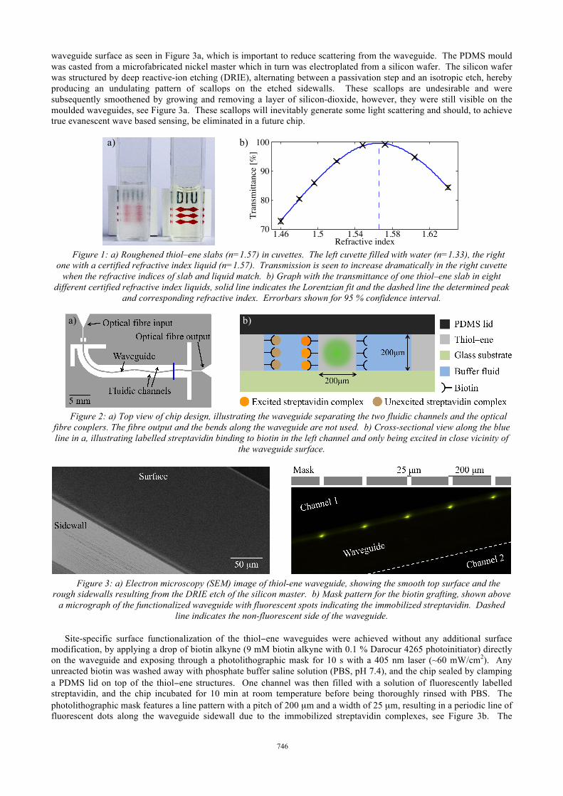
The refractive indices of thiol−ene slabs were determined by the modified immersion method developed by Nussbaumer et al. [6]. This method utilizes the concept of refractive index matching between a solid and a surrounding liquid, as the transmittance through a solid immersed in liquids of varying refractive indices peaks when the refractive index of solid and liquid match. By measuring the transmittance in a series of certified liquids, the refractive index is determined by a least square fit of a Lorentzian curve to the peak, enabling an accurate determination even when the exact index-matching liquid is not used. To increases the scattering for non-matching liquids, hereby making the peak more pronounced, the mould for the thiol−ene slabs were initially roughened with P80 sandpaper, providing a surface roughness of ±10 µm from the surface average. A simple illustration of the index matching concept resulting in increased transmittance is seen in Figure 1a, while a typical set of transmittance values and the corresponding Lorentzian fit is seen in Figure 1b. The refractive index of uncured thiol−ene mixtures were determined with an Abbé refractometer.
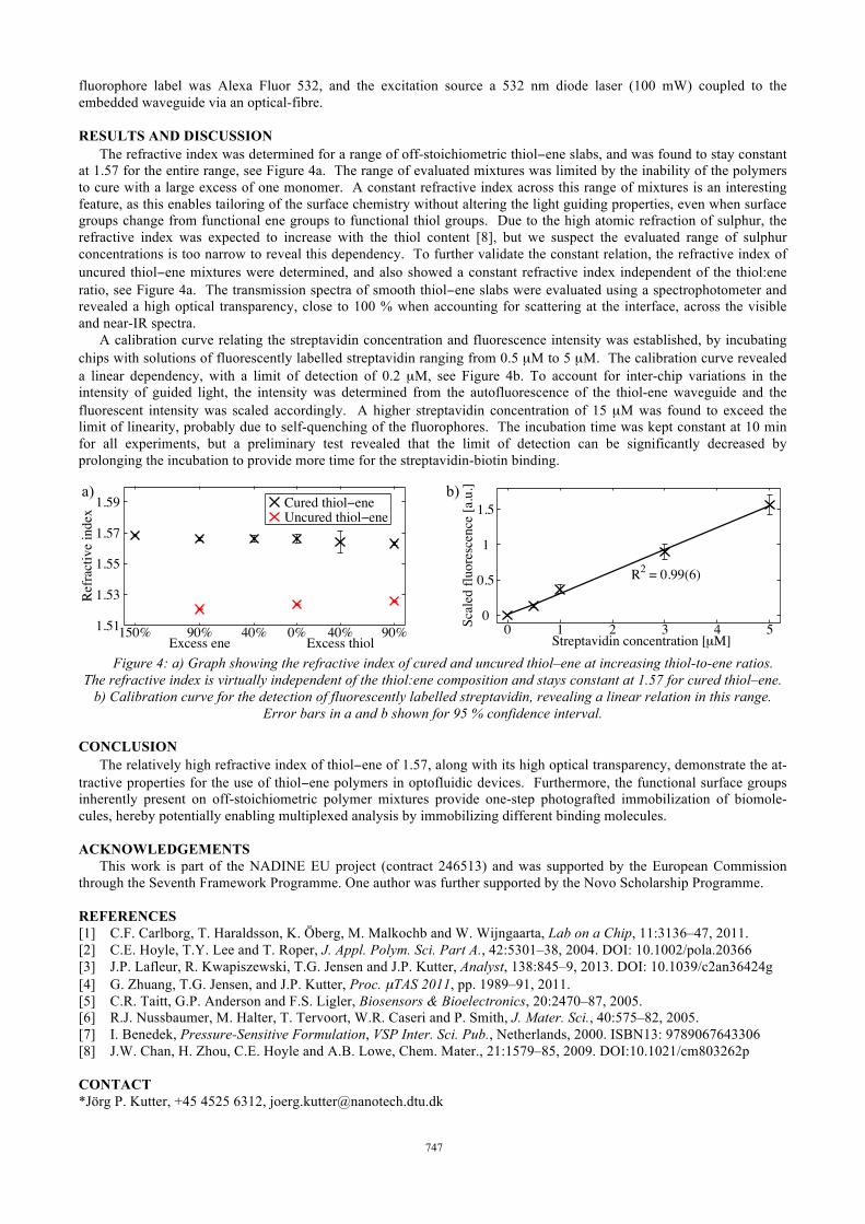
A thiol−ene chip was designed, featuring an embedded waveguide in contact with two fluidic channels and a coupling structure to connect the external optical fibres, see Figure 2a. A cross-section of the device is seen in Figure 2b, illustrating the covalently bonded biotin and immobilized streptavidin-fluorophore complexes on the waveguide surface. The thiol−ene chips were prepared on glass substrates by clamping a PDMS mould to the substrate and injecting the thiol−ene mixture into the mould cavities, followed by UV curing through the PDMS and an additional UV exposure after removing the PDMS to ensure complete bulk polymerization (3 min in total, ~40 mW/cm2 at 365 nm). The monomer ratios were adjusted to obtain 40 % excess thiol groups, providing a surface density of approximately 20 thiol-groups/nm2 [3]. The UV curing was performed in ambient air conditions, which can result in oxygen inhibiting the curing by forming alkyl-peroxy radicals that terminate the polymerization reaction [7]. This oxygen inhibition was avoided by using a UV source with high output intensity below 300 nm, as these wavelengths break the peroxide bonds and generate a reactive alkoxy radical which continues the polymerization reaction [7]. The result was a very smooth
waveguide surface as seen in Figure 3a, which is important to reduce scattering from the waveguide. The PDMS mould was casted from a microfabricated nickel master which in turn was electroplated from a silicon wafer. The silicon wafer was structured by deep reactive-ion etching (DRIE), alternating between a passivation step and an isotropic etch, hereby producing an undulating pattern of scallops on the etched sidewalls. These scallops are undesirable and were subsequently smoothened by growing and removing a layer of silicon-dioxide, however, they were still visible on the moulded waveguides, see Figure 3a. These scallops will inevitably generate some light scattering and should, to achieve true evanescent wave based sensing, be eliminated in a future chip.
70
80
90
100
1.46 1.5 1.54 1.58 1.62Refractive index
Tran
smitt
ance
[%]
Figure 1: a) Roughened thiol–ene slabs (n=1.57) in cuvettes. The left cuvette filled with water (n=1.33), the right
one with a certified refractive index liquid (n=1.57). Transmission is seen to increase dramatically in the right cuvette when the refractive indices of slab and liquid match. b) Graph with the transmittance of one thiol–ene slab in eight
different certified refractive index liquids, solid line indicates the Lorentzian fit and the dashed line the determined peak and corresponding refractive index. Errorbars shown for 95 % confidence interval.
Figure 2: a) Top view of chip design, illustrating the waveguide separating the two fluidic channels and the optical
fibre couplers. The fibre output and the bends along the waveguide are not used. b) Cross-sectional view along the blue line in a, illustrating labelled streptavidin binding to biotin in the left channel and only being excited in close vicinity of
the waveguide surface.
Figure 3: a) Electron microscopy (SEM) image of thiol-ene waveguide, showing the smooth top surface and the
rough sidewalls resulting from the DRIE etch of the silicon master. b) Mask pattern for the biotin grafting, shown above a micrograph of the functionalized waveguide with fluorescent spots indicating the immobilized streptavidin. Dashed
line indicates the non-fluorescent side of the waveguide.
Site-specific surface functionalization of the thiol−ene waveguides were achieved without any additional surface modification, by applying a drop of biotin alkyne (9 mM biotin alkyne with 0.1 % Darocur 4265 photoinitiator) directly on the waveguide and exposing through a photolithographic mask for 10 s with a 405 nm laser (~60 mW/cm2). Any unreacted biotin was washed away with phosphate buffer saline solution (PBS, pH 7.4), and the chip sealed by clamping a PDMS lid on top of the thiol−ene structures. One channel was then filled with a solution of fluorescently labelled streptavidin, and the chip incubated for 10 min at room temperature before being thoroughly rinsed with PBS. The photolithographic mask features a line pattern with a pitch of 200 µm and a width of 25 µm, resulting in a periodic line of fluorescent dots along the waveguide sidewall due to the immobilized streptavidin complexes, see Figure 3b. The
a) b)
a) b)
746
fluorophore label was Alexa Fluor 532, and the excitation source a 532 nm diode laser (100 mW) coupled to the embedded waveguide via an optical-fibre.
RESULTS AND DISCUSSION
The refractive index was determined for a range of off-stoichiometric thiol−ene slabs, and was found to stay constant at 1.57 for the entire range, see Figure 4a. The range of evaluated mixtures was limited by the inability of the polymers to cure with a large excess of one monomer. A constant refractive index across this range of mixtures is an interesting feature, as this enables tailoring of the surface chemistry without altering the light guiding properties, even when surface groups change from functional ene groups to functional thiol groups. Due to the high atomic refraction of sulphur, the refractive index was expected to increase with the thiol content [8], but we suspect the evaluated range of sulphur concentrations is too narrow to reveal this dependency. To further validate the constant relation, the refractive index of uncured thiol−ene mixtures were determined, and also showed a constant refractive index independent of the thiol:ene ratio, see Figure 4a. The transmission spectra of smooth thiol−ene slabs were evaluated using a spectrophotometer and revealed a high optical transparency, close to 100 % when accounting for scattering at the interface, across the visible and near-IR spectra.
A calibration curve relating the streptavidin concentration and fluorescence intensity was established, by incubating chips with solutions of fluorescently labelled streptavidin ranging from 0.5 µM to 5 µM. The calibration curve revealed a linear dependency, with a limit of detection of 0.2 µM, see Figure 4b. To account for inter-chip variations in the intensity of guided light, the intensity was determined from the autofluorescence of the thiol-ene waveguide and the fluorescent intensity was scaled accordingly. A higher streptavidin concentration of 15 µM was found to exceed the limit of linearity, probably due to self-quenching of the fluorophores. The incubation time was kept constant at 10 min for all experiments, but a preliminary test revealed that the limit of detection can be significantly decreased by prolonging the incubation to provide more time for the streptavidin-biotin binding.
1.51
1.53
1.55
1.57
1.59
150% 90% 40% 0% 40% 90%Excess ene Excess thiol
Ref
ract
ive
inde
x
Cured thiolïeneUncured thiolïene
R2 = 0.99(6)
0
0.5
1
1.5
0 1 2 3 4 5Streptavidin concentration [µM]
Scal
ed fl
uore
scen
ce [a
.u.]
Figure 4: a) Graph showing the refractive index of cured and uncured thiol–ene at increasing thiol-to-ene ratios.
The refractive index is virtually independent of the thiol:ene composition and stays constant at 1.57 for cured thiol–ene. b) Calibration curve for the detection of fluorescently labelled streptavidin, revealing a linear relation in this range.
Error bars in a and b shown for 95 % confidence interval.
CONCLUSION The relatively high refractive index of thiol−ene of 1.57, along with its high optical transparency, demonstrate the at-
tractive properties for the use of thiol−ene polymers in optofluidic devices. Furthermore, the functional surface groups inherently present on off-stoichiometric polymer mixtures provide one-step photografted immobilization of biomole-cules, hereby potentially enabling multiplexed analysis by immobilizing different binding molecules. ACKNOWLEDGEMENTS
This work is part of the NADINE EU project (contract 246513) and was supported by the European Commission through the Seventh Framework Programme. One author was further supported by the Novo Scholarship Programme. REFERENCES [1] C.F. Carlborg, T. Haraldsson, K. Öberg, M. Malkochb and W. Wijngaarta, Lab on a Chip, 11:3136–47, 2011. [2] C.E. Hoyle, T.Y. Lee and T. Roper, J. Appl. Polym. Sci. Part A., 42:5301–38, 2004. DOI: 10.1002/pola.20366 [3] J.P. Lafleur, R. Kwapiszewski, T.G. Jensen and J.P. Kutter, Analyst, 138:845–9, 2013. DOI: 10.1039/c2an36424g [4] G. Zhuang, T.G. Jensen, and J.P. Kutter, Proc. µTAS 2011, pp. 1989–91, 2011. [5] C.R. Taitt, G.P. Anderson and F.S. Ligler, Biosensors & Bioelectronics, 20:2470–87, 2005. [6] R.J. Nussbaumer, M. Halter, T. Tervoort, W.R. Caseri and P. Smith, J. Mater. Sci., 40:575–82, 2005. [7] I. Benedek, Pressure-Sensitive Formulation, VSP Inter. Sci. Pub., Netherlands, 2000. ISBN13: 9789067643306 [8] J.W. Chan, H. Zhou, C.E. Hoyle and A.B. Lowe, Chem. Mater., 21:1579–85, 2009. DOI:10.1021/cm803262p CONTACT *Jörg P. Kutter, +45 4525 6312, [email protected]


![Thiol-Ene Clickable Gelatin: A Platform Bioink for Multiple 3D Biofabrication Technologiesdownload.xuebalib.com/k3eyvSf1HRK.pdf · [3b,5] Thiol–ene click chemistry herein represents](https://static.documents.pub/doc/80x56/60e592cc65b892391f6cc759/thiol-ene-clickable-gelatin-a-platform-bioink-for-multiple-3d-biofabrication-3b5.jpg)


