27
Fundamentals of nanomaterials Lecture 5 Lecture 5 MTX9100 Nanomaterjalid OUTLINE - What can nanomaterials be? - What is a dimension? - Does size mean a lot? -What is a potential well? 1
Fundamentals of
nanomaterials
Lecture 5Lecture 5MTX9100
NanomaterjalidOUTLINE
-What can nanomaterials be?-What is a dimension? - Does size mean a lot?-What is a potential well?
1
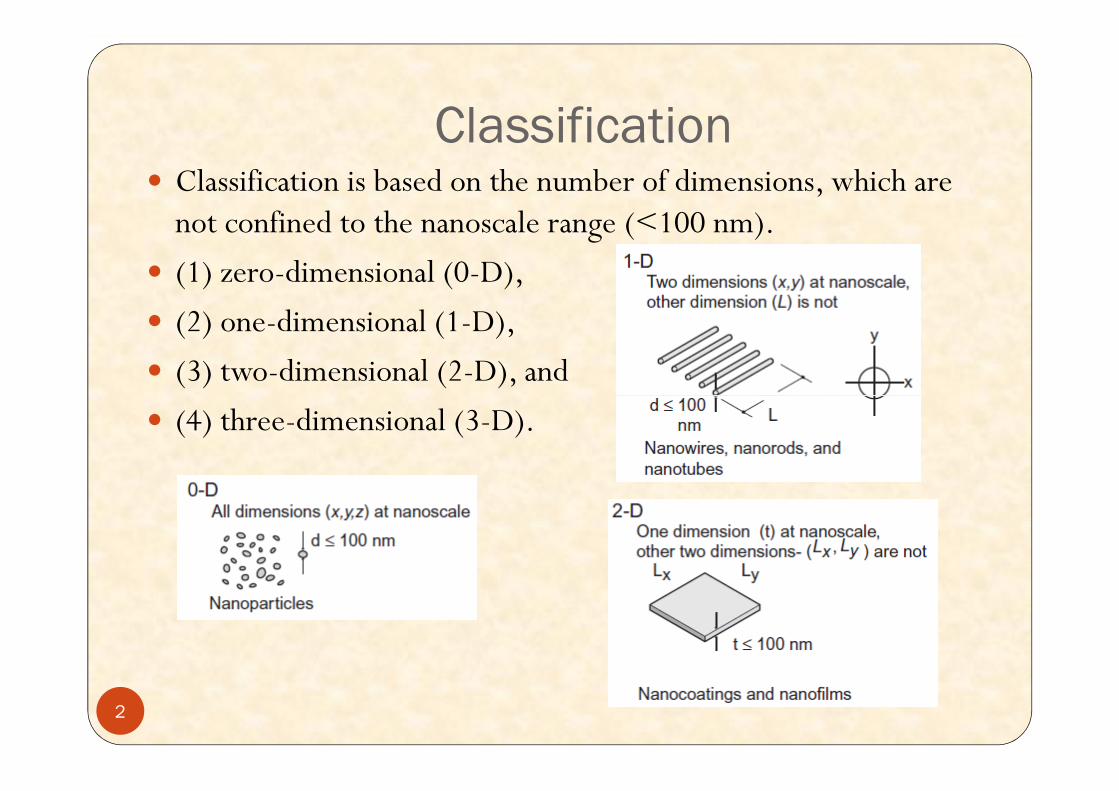
Classification� Classification is based on the number of dimensions, which are
not confined to the nanoscale range (<100 nm).
� (1) zero-dimensional (0-D),
� (2) one-dimensional (1-D),
� (3) two-dimensional (2-D), and
� (4) three-dimensional (3-D).
2

Zero-dimensional nanomaterials� Materials wherein all the dimensions are measured within the
nanoscale (no dimensions, or 0-D, are larger than 100 nm).� The most common representation of zero-dimensional
nanomaterials are nanoparticles.� Nanoparticles can:Nanoparticles
� Be amorphous or crystalline� Be single crystalline or polycrystalline� Be composed of single or multi-chemical elements� Exhibit various shapes and forms� Exist individually or incorporated in a matrix� Be metallic, ceramic, or polymeric
3

One-dimensional nanomaterials� One dimension that is outside the nanoscale. � This leads to needle like-shaped nanomaterials.� 1-D materials include nanotubes, nanorods, and nanowires.
� 1-D nanomaterials can be� 1-D nanomaterials can be� Amorphous or crystalline� Single crystalline or polycrystalline� Chemically pure or impure� Standalone materials or embedded in within another medium� Metallic, ceramic, or polymeric
4

Two-dimensional nanomaterials
� Two of the dimensions are not confined to the nanoscale.
� 2-D nanomaterials exhibit plate-like shapes.
� Two-dimensional nanomaterials include nanofilms, nanolayers, and nanocoatings.
� 2-D nanomaterials can be:� 2-D nanomaterials can be:
� Amorphous or crystalline
� Made up of various chemical compositions
� Used as a single layer or as multilayer structures
� Deposited on a substrate
� Integrated in a surrounding matrix material
� Metallic, ceramic, or polymeric5

Three-dimensional nanomaterials� Bulk nanomaterials are materials that are not confined to the
nanoscale in any dimension. These materials are thus characterized by having three arbitrarily dimensions above 100 nm.
� Materials possess a nanocrystalline structure or involve the presence of features at the nanoscale. presence of features at the nanoscale.
� In terms of nanocrystalline structure, bulk nanomaterials can be composed of a multiple arrangement of nanosize crystals, most typically in different orientations.
� With respect to the presence of features at the nanoscale, 3-D nanomaterials can contain dispersions of nanoparticles, bundles of nanowires, and nanotubes as well as multinanolayers.
6

ThreeThreeThreeThree----dimensional space showing the relationships dimensional space showing the relationships dimensional space showing the relationships dimensional space showing the relationships
among 0among 0among 0among 0----D, 1D, 1D, 1D, 1----D, 2D, 2D, 2D, 2----D, and D, and D, and D, and 3333----D D D D nanomaterialsnanomaterialsnanomaterialsnanomaterials....
7
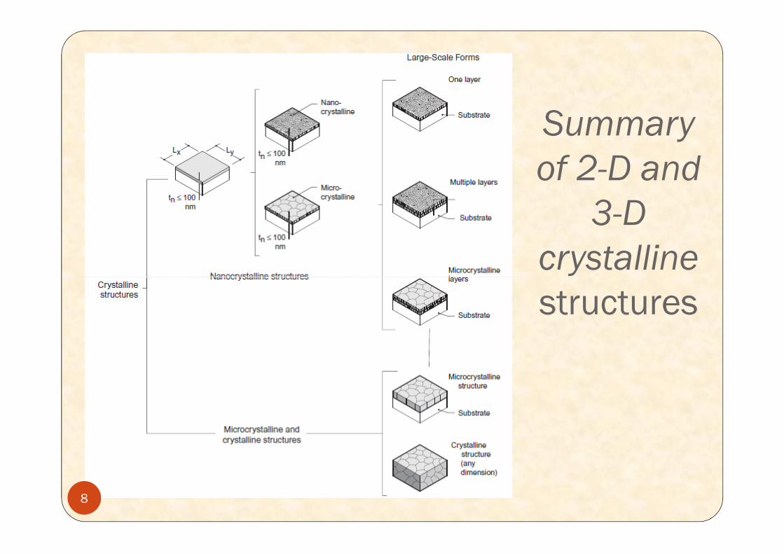
Summary
of 2-D and
3-D
crystalline crystalline
structures
8
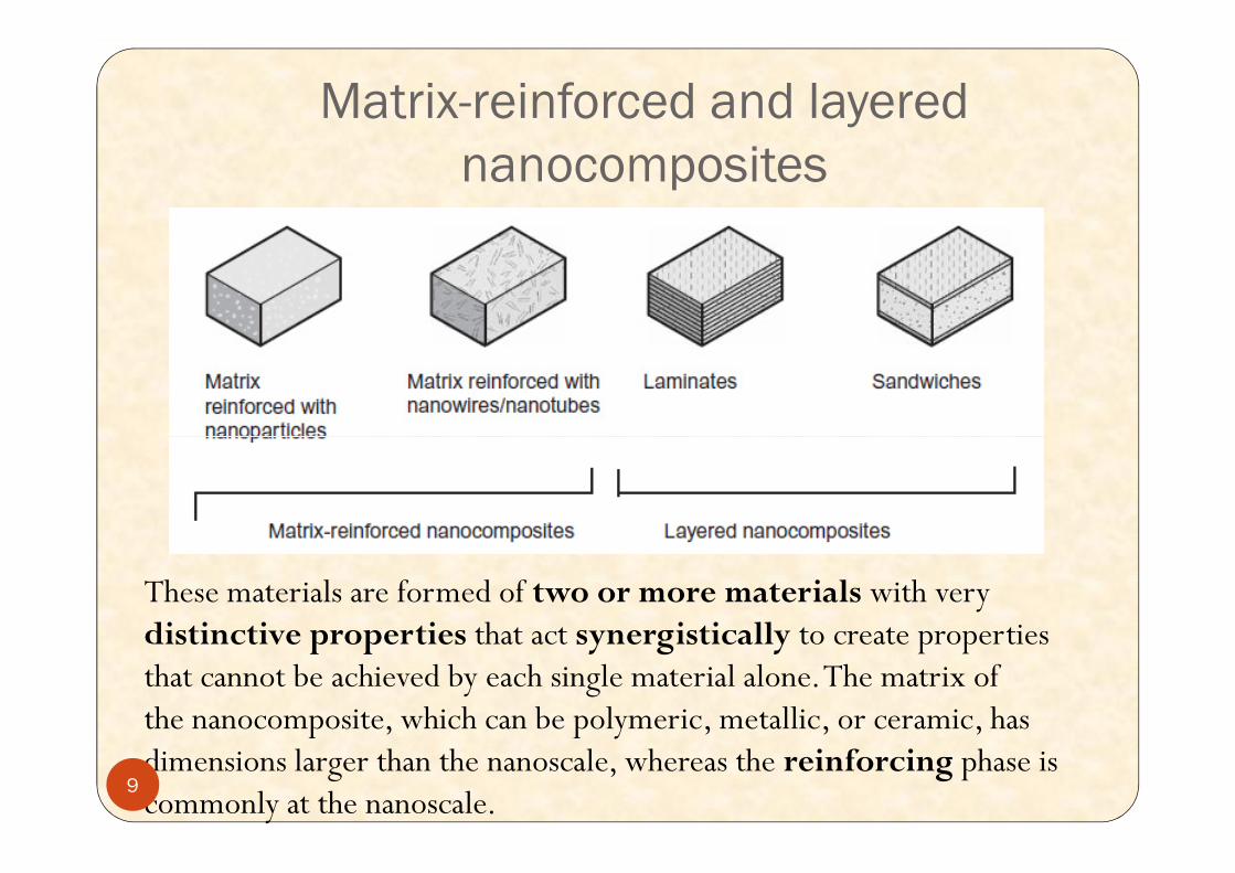
Matrix-reinforced and layered
nanocomposites
These materials are formed of two or more materials with verydistinctive properties that act synergistically to create propertiesthat cannot be achieved by each single material alone. The matrix ofthe nanocomposite, which can be polymeric, metallic, or ceramic, has dimensions larger than the nanoscale, whereas the reinforcing phase is commonly at the nanoscale.
9
Carbon� Carbon is a basic element of life
� Carbon is special because of its ability to bond to many elements in many different ways
� It is the sixth most abundant element in the universeuniverse
� The most known types of carbon materials: diamond; graphite; fullerenes; and carbon nanotubes
10

Carbon materialsCarbon materialsCarbon materialsCarbon materialsDiamond and Diamond and
graphite are two allotropes of carbon:
pure forms of the same element that differ in structure.
2s and 2p electrons available for bonding
11

DIAMOND- chemical bonding is purely covalent- highly symmetrical unit cell- extremely hard- low electrical conductivity- high thermal conductivity (superior)- optically transparent- used as gemstones and industrialgrinding, machining and cuttinggrinding, machining and cutting
12
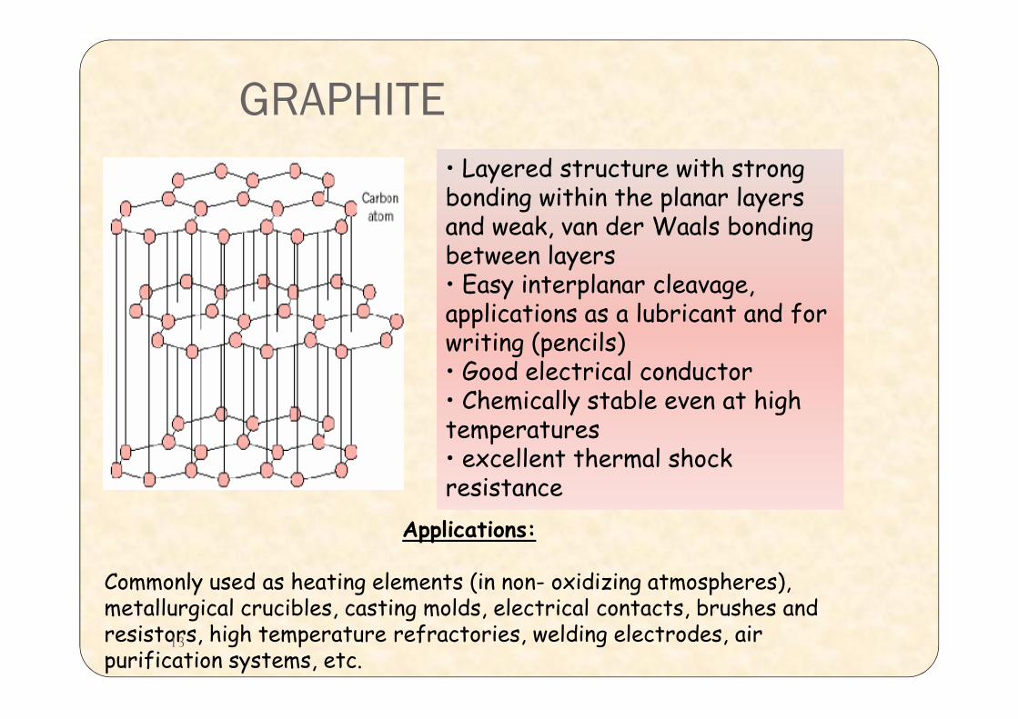
GRAPHITE
• Layered structure with strong bonding within the planar layers and weak, van der Waals bonding between layers• Easy interplanar cleavage, applications as a lubricant and forwriting (pencils)• Good electrical conductor• Good electrical conductor• Chemically stable even at high temperatures• excellent thermal shock resistance
Applications:
Commonly used as heating elements (in non- oxidizing atmospheres),metallurgical crucibles, casting molds, electrical contacts, brushes andresistors, high temperature refractories, welding electrodes, air purification systems, etc.
13
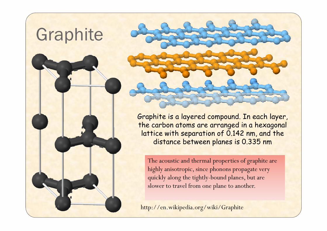
Graphite
Graphite is a layered compound. In each layer,
http://en.wikipedia.org/wiki/Graphite
Graphite is a layered compound. In each layer, the carbon atoms are arranged in a hexagonal lattice with separation of 0.142 nm, and the
distance between planes is 0.335 nm
The acoustic and thermal properties of graphite are highly anisotropic, since phonons propagate very quickly along the tightly-bound planes, but are slower to travel from one plane to another.
14

GrapheneGraphene is an one-atom-thick planar sheet of sp2-bonded carbonatoms that are densely packed in a honeycomb crystal lattice. It can be viewed as an atomic-scale chicken wire made of carbon atoms and their bonds
The carbon-carbon bond length in graphene is about 0.142 nm. Graphene is the basic structural element of some carbon allotropes including graphite, carbon nanotubes and fullerenes.
15

Allotropes of carbonAllotropes of carbonAllotropes of carbonAllotropes of carbon
a) diamond b) graphite c) lonsdaleite(hexagonal diamond)
d) - f) fullerenes
3D
0Dd) - f) fullerenes (C60, C540, C70);
g) amorphous carbon
h) carbon nanotube
Wikipedia16
1D
0D
2D - ???

17

SCIENCE, June 2010
� If there's a rock star in the world of materials, it's graphene: single-atom–thick sheets of carbon prized for its off-the-charts ability to conduct electrons and for being all but transparent.
� Those qualities make graphene a tantalizing alternative for use as a transparent conductor, the sort now found in use as a transparent conductor, the sort now found in everything from computer displays and flat panel TVs to ATM touch screens and solar cells.
� But the material has been tough to manufacture in anything larger than flakes a few centimeters across.
� Now researchers have managed to create rectangular sheets of graphene 76 centimeters in the diagonal direction and even use them to create a working touch-screen display
18

Quantum effects� The overall behavior of bulk crystalline materials changes when
the dimensions are reduced to the nanoscale. � For 0-D nanomaterials, where all the dimensions are at the
nanoscale, an electron is confined in 3-D space. No electron delocalization (freedom to move) occurs. For 1-D nanomaterials, electron confinement occurs in 2-D,
19
� For 1-D nanomaterials, electron confinement occurs in 2-D, whereas delocalization takes place along the long axis of the nanowire/rod/tube.
� In the case of 2-D nanomaterials, the conduction electrons will be confined across the thickness but delocalized in the plane of the sheet.

Electrons confinement� For 0-D nanomaterials the electrons are fully confined.
� For 3-D nanomaterials the electrons are fully delocalized.
� In 1-D and 2-D nanomaterials, electron confinement and delocalization coexist.
� The effect of confinement on the resulting energy states can
20
� The effect of confinement on the resulting energy states can be calculated by quantum mechanics, as the “particle in the box” problem. An electron is considered to exist inside of an infinitely deep potential well (region of negative energies), from which it cannot escape and is confined by the dimensions of the nanostructure.

Energies
21
where h¯ ≡ h/2π, h is Planck’s constant, m is the mass of the electron, L is the width (confinement) of the infinitely deep potential well, and nx, ny, and nz are the principal quantum numbers in the three dimensions x, y, and z.
The smaller the dimensions of the nanostructure (smaller L), the wider is the separation between the
energy levels, leading to a spectrum ofdiscreet energies.

What’s different at the nanoscale?What’s different at the nanoscale?What’s different at the nanoscale?What’s different at the nanoscale?
Each of the different sized arrangement of gold atoms absorbs and reflects light differently based on its energy
levels, which are determined by size and bonding arrangement. This is true for many materials when the
particles have a size that is less than 100 nanometers in at least one dimension.
22

Energy levels in infinite
quantum well
23

The finite potential well For the finite potential well, the solution to the Schrodinger equation gives a wavefunction with an exponentially decaying penetration into the classically forbidden region.
Confining a particle to a smaller space requires a larger confinement energy. Since the wavefunction penetration
effectively "enlarges the box", the finite well energy levels are lower than those
for the infinite well. for the infinite well.
The solution for -L/2 < x < L/2 and elsewhere must satisfy the equation
With the substitution
24

The finite potential well
25

Comparison of Infinite and Finite
Potential Wells
Eigenstates with E < V0 are bound or localized. Eigenstates with E > V0 are unbound or delocalized 26

Electron energy densityThe behavior of electrons in solids depends upon the distribution of energy among the electrons:
This distribution determines the probability that a given energy state will This distribution determines the probability that a given energy state will be occupied, but must be multiplied by the density of states function to weight the probability by the number of states available at a given energy.
Density of states in (a) metal, (b) semimetal (e.g.
graphite).
27


