Chalmers University of Technology Department of Microtechnology an Nanoscience Future and Emerging Semiconductor Technologies By Björn Carlberg, David Gustafsson, Erik Eriksson, Mohammad Najmzadeh, and Rashid Farivar (Group 5) A report submitted as a project work for the course “Semiconductor Materials Physics FMI040” 1
Transcript
Chalmers University of Technology
Department of Microtechnology an Nanoscience
Future and Emerging Semiconductor Technologies
By
Björn Carlberg, David Gustafsson, Erik Eriksson, Mohammad Najmzadeh, and Rashid Farivar
(Group 5)
A report submitted as a project work for the course “Semiconductor Materials Physics FMI040”
1
1. Molecular Electronics and Nanotechnology [1, 2, 3, 4, and 5] 1.1. Limitation of Silicon
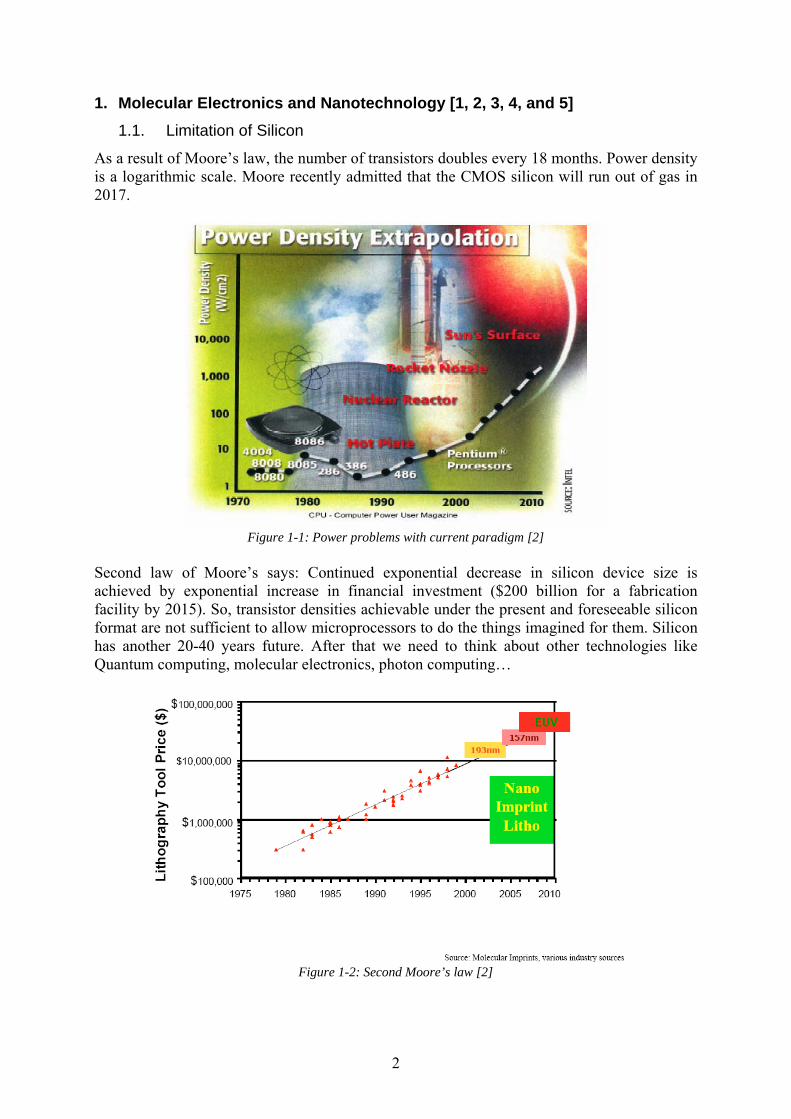
As a result of Moore’s law, the number of transistors doubles every 18 months. Power density is a logarithmic scale. Moore recently admitted that the CMOS silicon will run out of gas in 2017.
Figure 1-1: Power problems with current paradigm [2]
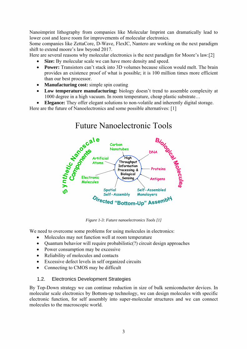
Second law of Moore’s says: Continued exponential decrease in silicon device size is achieved by exponential increase in financial investment ($200 billion for a fabrication facility by 2015). So, transistor densities achievable under the present and foreseeable silicon format are not sufficient to allow microprocessors to do the things imagined for them. Silicon has another 20-40 years future. After that we need to think about other technologies like Quantum computing, molecular electronics, photon computing…
Figure 1-2: Second Moore’s law [2]
2
Nanoimprint lithography from companies like Molecular Imprint can dramatically lead to lower cost and leave room for improvements of molecular electronics. Some companies like ZettaCore, D-Wave, FlexIC, Nantero are working on the next paradigm shift to extend moore’s law beyond 2017. Here are several reasons why molecular electronics is the next paradigm for Moore’s law:[2]
• Size: By molecular scale we can have more density and speed. • Power: Transistors can’t stack into 3D volumes because silicon would melt. The brain
provides an existence proof of what is possible; it is 100 million times more efficient than our best processor.
• Manufacturing cost: simple spin coating • Low temperature manufacturing: biology doesn’t trend to assemble complexity at
1000 degree in a high vacuum. In room temperature, cheap plastic substrate… • Elegance: They offer elegant solutions to non-volatile and inherently digital storage.
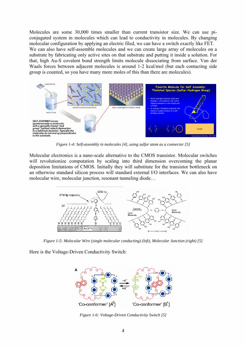
Here are the future of Nanoelectronics and some possible alternatives: [1]
Future Nanoelectronic Tools
Spatial Self-Assembly
Self-Assembled Monolayers
ArtificialAtoms
Carbon Nanotubes
DNA
Electronic Molecules
Proteins
Antigens
High Throughput Information Processing & Biological Sensing
Figure 1-3: Future nanoelectronics Tools [1]
We need to overcome some problems for using molecules in electronics:
• Molecules may not function well at room temperature • Quantum behavior will require probabilistic(?) circuit design approaches • Power consumption may be excessive • Reliability of molecules and contacts • Excessive defect levels in self organized circuits • Connecting to CMOS may be difficult 1.2. Electronics Development Strategies
By Top-Down strategy we can continue reduction in size of bulk semiconductor devices. In molecular scale electronics by Bottom-up technology, we can design molecules with specific electronic function, for self assembly into super-molecular structures and we can connect molecules to the macroscopic world.
3
Molecules are some 30,000 times smaller than current transistor size. We can use pi-conjugated system in molecules which can lead to conductivity in molecules. By changing molecular configuration by applying an electric filed, we can have a switch exactly like FET. We can also have self-assemble molecules and we can create large array of molecules on a substrate by fabricating only active sites on that substrate and putting it inside a solution. For that, high Au-S covalent bond strength limits molecule dissociating from surface. Van der Waals forces between adjacent molecules is around 1-2 kcal/mol (but each contacting side group is counted, so you have many more moles of this than there are molecules).
Supramolecular Chemistry, UAF, 2005
Favorite Molecule for Self Assembly: Favorite Molecule for Self Assembly: ThiolatedThiolated Species (SulfurSpecies (Sulfur--Hydrogen Group)Hydrogen Group)
• Bond strength between gold and thiolate = 44 kcal/mol, one of the highest between a non-metal and a metal
• In solution, thiolated molecule will bond to a gold surface in a self-limiting reaction
Gold!
Figure 1-4: Self-assembly in molecules [4], using sulfur atom as a connector [5]
Molecular electronics is a nano-scale alternative to the CMOS transistor. Molecular switches will revolutionize computation by scaling into third dimension overcoming the planar deposition limitations of CMOS. Initially they will substitute for the transistor bottleneck on an otherwise standard silicon process will standard external I/O interfaces. We can also have molecular wire, molecular junction, resonant tunneling diode…
Figure 1-5: Molecular Wire (single molecular conducting) (left), Molecular Junction (right) [5] Here is the Voltage-Driven Conductivity Switch:
Suspending carbon nanotubes above metal electrodes on silicon can create high density non-volatile memory chips. Carbon nanotubes are small (10atom wide), 30 times stronger than steel at 1/6 of weight, and perform the functions of wires, capacitors, and transistors with better speed, power, density and cost.
Electrode 2Electrode 1
CNT
VDS
VG
-0.1 0.0 0.1-20.0
-10.0
0.0
10.0
20.0
SETsSETs from from CNTsCNTs
I (nA
)
VDS (V)
4.2 K 15 K 27 K
-0.1 0 0.1
VSD (V)
20
10
0
-10
-20
I SD
(nA)
-35 -30 -250.0
1.0
2.0
3.0
4.0
5.0
I (nA
)
V (back gate) (V)
4.4 K 20 K 25 K 28 K 31 K 35 K
G
Figure 1-8: I-V characteristics curve for a CNT structure [1]
5
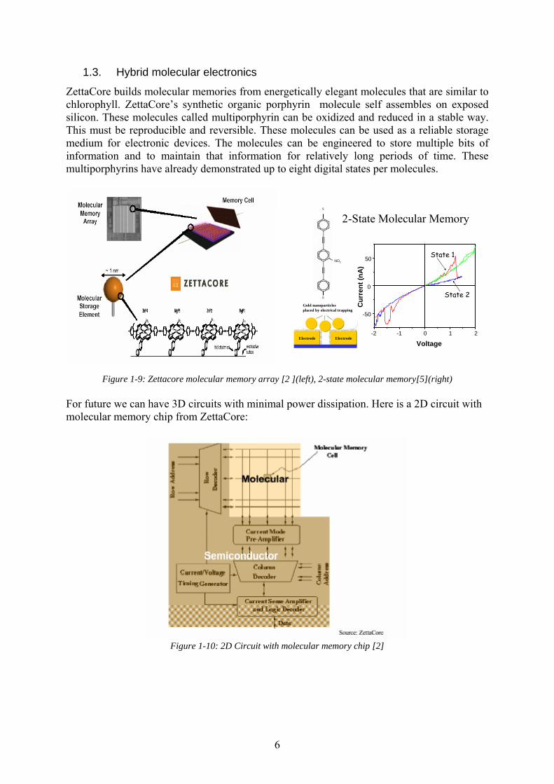
1.3. Hybrid molecular electronics
ZettaCore builds molecular memories from energetically elegant molecules that are similar to chlorophyll. ZettaCore’s synthetic organic porphyrin molecule self assembles on exposed silicon. These molecules called multiporphyrin can be oxidized and reduced in a stable way. This must be reproducible and reversible. These molecules can be used as a reliable storage medium for electronic devices. The molecules can be engineered to store multiple bits of information and to maintain that information for relatively long periods of time. These multiporphyrins have already demonstrated up to eight digital states per molecules.
For future we can have 3D circuits with minimal power dissipation. Here is a 2D circuit with molecular memory chip from ZettaCore:
Figure 1-10: 2D Circuit with molecular memory chip [2]
6
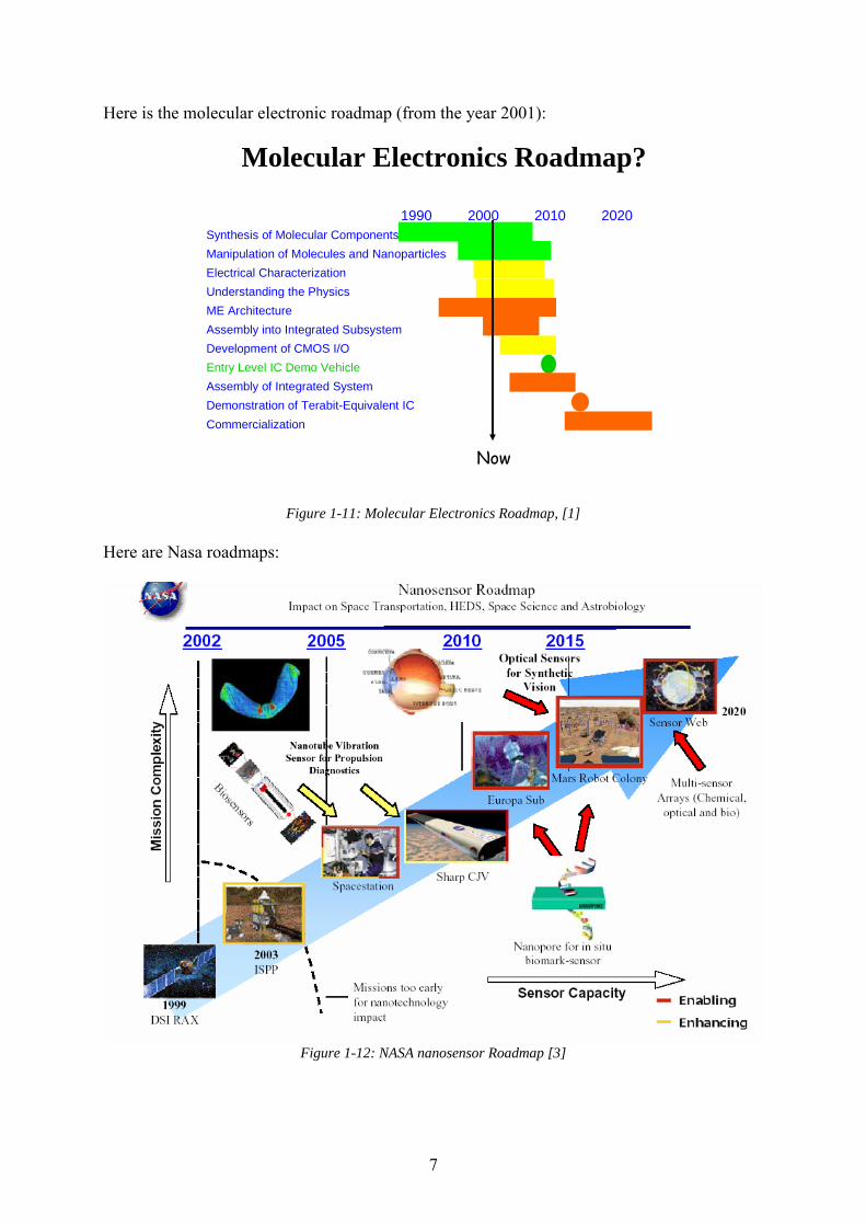
Here is the molecular electronic roadmap (from the year 2001):
Molecular Electronics Roadmap?
1990 2000 2010 2020Synthesis of Molecular ComponentsManipulation of Molecules and NanoparticlesElectrical CharacterizationUnderstanding the PhysicsME ArchitectureAssembly into Integrated SubsystemDevelopment of CMOS I/OEntry Level IC Demo VehicleAssembly of Integrated SystemDemonstration of Terabit-Equivalent ICCommercialization
Now
Figure 1-11: Molecular Electronics Roadmap, [1]
Here are Nasa roadmaps:
Figure 1-12: NASA nanosensor Roadmap [3]
7
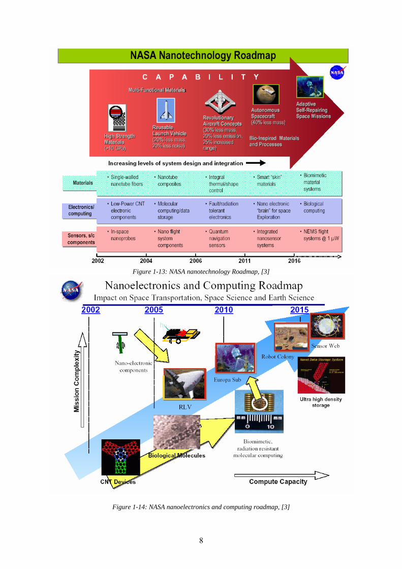
Figure 1-13: NASA nanotechnology Roadmap, [3]
Figure 1-14: NASA nanoelectronics and computing roadmap, [3]
8
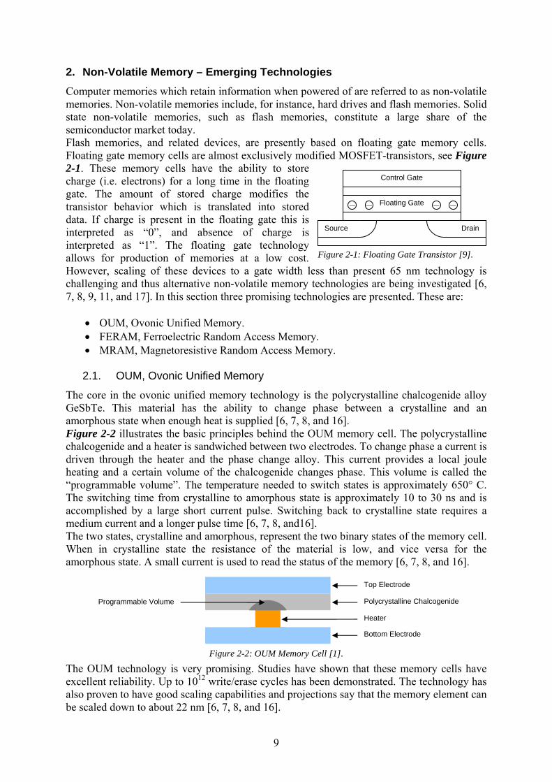
2. Non-Volatile Memory – Emerging Technologies Computer memories which retain information when powered of are referred to as non-volatile memories. Non-volatile memories include, for instance, hard drives and flash memories. Solid state non-volatile memories, such as flash memories, constitute a large share of the semiconductor market today. Flash memories, and related devices, are presently based on floating gate memory cells. Floating gate memory cells are almost exclusively modified MOSFET-transistors, see Figure 2-1. These memory cells have the ability to store charge (i.e. electrons) for a long time in the floating gate. The amount of stored charge modifies the transistor behavior which is translated into stored data. If charge is present in the floating gate this is interpreted as “0”, and absence of charge is interpreted as “1”. The floating gate technology allows for production of memories at a low cost. However, scaling of these devices to a gate width less than present 65 nm technology is challenging and thus alternative non-volatile memory technologies are being investigated [6, 7, 8, 9, 11, and 17]. In this section three promising technologies are presented. These are:
The core in the ovonic unified memory technology is the polycrystalline chalcogenide alloy GeSbTe. This material has the ability to change phase between a crystalline and an amorphous state when enough heat is supplied [6, 7, 8, and 16]. Figure 2-2 illustrates the basic principles behind the OUM memory cell. The polycrystalline chalcogenide and a heater is sandwiched between two electrodes. To change phase a current is driven through the heater and the phase change alloy. This current provides a local joule heating and a certain volume of the chalcogenide changes phase. This volume is called the “programmable volume”. The temperature needed to switch states is approximately 650° C. The switching time from crystalline to amorphous state is approximately 10 to 30 ns and is accomplished by a large short current pulse. Switching back to crystalline state requires a medium current and a longer pulse time [6, 7, 8, and16]. The two states, crystalline and amorphous, represent the two binary states of the memory cell. When in crystalline state the resistance of the material is low, and vice versa for the amorphous state. A small current is used to read the status of the memory [6, 7, 8, and 16]. Top Electrode
Figure 2-2: OUM Memory Cell [1]. The OUM technology is very promising. Studies have shown that these memory cells have excellent reliability. Up to 1012 write/erase cycles has been demonstrated. The technology has also proven to have good scaling capabilities and projections say that the memory element can be scaled down to about 22 nm [6, 7, 8, and 16].
9
Currently research is focused on the physics of the memory cell, reducing switching current and future manufacture of memory arrays [6, 7, 8, and 16].
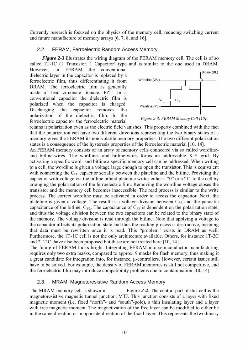
2.2. FERAM, Ferroelectric Random Access Memory
Figure 2-3 illustrates the wiring diagram of the FERAM memory cell. The cell is of so called 1T-1C (1 Transistor, 1 Capacitor) type and is similar to the one used in DRAM. However, in FERAM the conventional dielectric layer in the capacitor is replaced by a ferroelectric film, thus differentiating it from DRAM. The ferroelectric film is generally made of lead zirconate titanate, PZT. In a conventional capacitor the dielectric film is polarized when the capacitor is charged. Discharging the capacitor removes the polarization of the dielectric film. In the ferroelectric capacitor the ferroelectric material retains it polarization even as the electric field vanishes. This property combined with the fact that the polarization can have two different directions representing the two binary states of a memory gives the FERAM its non-volatile memory properties. The two different polarization states is a consequence of the hysteresis properties of the ferroelectric material [10, 14].
VC –
+
Bitline (BL)
CFE
Plateline (PL)
Wordline (WL)
Figure 2-3: FERAM Memory Cell [10].
An FERAM memory consists of an array of memory cells connected via so called wordline- and bitline-wires. The wordline- and bitline-wires forms an addressable X-Y grid. By activating a specific word- and bitline a specific memory cell can be addressed. When writing to a cell, the wordline is given a voltage large enough to open the transistor. This is equivalent with connecting the CFE capacitor serially between the plateline and the bitline. Providing the capacitor with voltage via the bitline or/and plateline writes either a “0” or a “1” to the cell by arranging the polarization of the ferroelectric film. Removing the wordline voltage closes the transistor and the memory cell becomes inaccessible. The read process is similar to the write process. The correct wordline must be activated in order to access the capacitor. Next, the plateline is given a voltage. The result is a voltage division between CFE and the parasitic capacitance of the bitline, CBL. The capacitance of CFE is dependent on the polarization state, and thus the voltage division between the two capacitors can be related to the binary state of the memory. The voltage division is read through the bitline. Note that applying a voltage to the capacitor affects its polarization state and thus the reading process is destructive, meaning that data must be rewritten once it is read. This “problem” exists in DRAM as well. Furthermore, the 1T-1C cell is not the only architecture available. Others, for instance 1T-2C and 2T-2C, have also been proposed but these are not treated here [10, 14]. The future of FERAM looks bright. Integrating FERAM into semiconductor manufacturing requires only two extra masks, compared to approx. 9 masks for flash memory, thus making it a great candidate for integration into, for instance, µ-controllers. However, certain issues still have to be solved. For example, the density of FERAM memories is still not competitive, and the ferroelectric film may introduce compatibility problems due to contamination [10, 14].
2.3. MRAM, Magnetoresistive Random Access Memory
The MRAM memory cell is shown in Figure 2-4. The central part of this cell is the magnetoresistive magnetic tunnel junction, MTJ. This junction consists of a layer with fixed magnetic moment (i.e. fixed “north”- and “south”-pole), a thin insulating layer and a layer with free magnetic moment. The magnetization of the free layer can be modified to either be in the same direction or in opposite direction of the fixed layer. This represents the two binary
10
states of the memory cell. A typical material for the free layer is NiFe. The insulation layer is typically made from aluminum oxide [12, 13, and 15]. As with FERAM, the cell is operated via a wordarray with the word- and bitlines perpendicular to each other. Thus, the array is X-Y-addressable and a particular memory cell is chosen by activating the correct word- and bitline. Writing to the cell is accomplished by driving current through the word- and bitline. The direction of the current determines the magnetic field around the conductor and this is used to affect the magnetization of the free layer in the desired direction. Only the cell which is affected by both the word- and bitline is subjected to enough magnetic flux to change the magnetization of the free layer. All other cells on the same lines remain unaffected. The reading operation is performed by first putting the transistor in on state and then biasing the bitline with approx. 0.3 V. A small current travels through the MTJ by tunneling of electrons through the thin insulating barrier. The current is proportional to the resistance of the MTJ. The resistance of the MTJ is dependent on the direction of the magnetization in the free layer relative to the fixed layer. Opposite direction gives a higher resistance and vice versa. Thus, the state of the memory cell can be determined by measuring the current in the bitline during the read operation [12, 13, and 15].
line and a bitline. The cells are placed in an
Wordline
Bitline
Tunnel Barrier Free Layer
Fixed Layer
Figure 2-4: MRAM Memory Cell [12].
As for the other discussed technologies, the MRAM technology has a future but some issues remain to be solved. One of these issues is related to current distribution in the word- and bitline during write operation. Another one is related to too low readout signal during read operation. However, fast progress is made due to great research efforts and prototypes have been demonstrated by both Infineon and NEC [12, 13, and 15].
2.4. Comparison between Emerging Memory Technologies
Table 2-1 provides a comparison between the technologies presented above. From the table it is obvious that OUM has a certain advantage over its competitors. The high write and read speed combined with excellent endurance and scaling is factors that provide this advantage. Technology OUM MRAM FERAM Endurance Write / Read >1012 / ∞ >1012 / ∞ 1012 / 1012
Read Non-destructive Non-destructive Destructive Direct Overwrite Yes Yes Yes Bit / Byte Write / Erase Yes Yes Yes Programming Energy Low Medium Medium Write / Erase / Read Time 10 ns / 50 ns / 20 ns 30 ns / 30 ns / 30 ns 80 ns / 80 ns / 80 ns Transistors High performance High performance Low performance CMOS Logic Compatibility Good Unknown High Voltage Required New Materials Yes Yes Yes Scalability Limits Lithography Current density Polarizable capacitor Multi-bit Storage Yes No No 3D Potential Yes Unknown Unknown Relative Cost Per Bit Low Unknown High
Table 2-1: Comparison Between Emerging Memory Technologies [2].
11
3. Spintronics
3.1. Introduction
As the downscaling of microelectronic devices continues the technology will, according to the famous Moore’s Law, in the next decade reach the fundamental limit of the atomic size [19]. Consequently, scientists are looking for new technologies that will enable increasing circuit performance after the limit is reached. Recently, researchers have begun considering the use of the electronic spin as information carrier, which offers a way to develop a new generation of devices combining standard microelectronics with spin-dependent effects [20]. These new devices would have advantages of nonvolatility, increased data processing speed, decreased electric power consumption and increased integration densities compared to the conventional semiconductor devices. Since the spin is already defined on a single electron, these devices should be able to downscale to very small dimensions [21].
3.2. Spin Devices
The discovery in 1988 of the giant magnetoresistive effect (GMR) is considered as the beginning of the new spin-based electronics, or spintronics, technology [20]. The effect is observed in thin-film materials of alternate ferromagnetic and nonmagnetic layers. The resistance of the material is high when the magnetic moments in the ferromagnetic layers are antialigned and low when they are aligned. A so called spin valve is a GMR-based device consisting of two ferromagnetic layers (alloys of nickel, iron and cobalt) sandwiching a thin layer of a nonmagnetic metal (usually copper). One of the two magnetic layers is ”pinned”, meaning that the magnetization in that layer is relatively insensitive to external magnetic fields. The other layer is called the”free” layer and its magnetization can be changed by application of relatively small fields. When the magnetization in the two layers change from parallel to antiparallel the resistance in the spin valve typically rises between 5 and 10%. The magnetic tunnel junction (MTJ) is another spin device consisting of two ferromagnetic layers separated by an insulator, commonly aluminium oxide [21]. Like the spin valve this tri-layer structure show a difference in resistance depending on the alignment of the magnetic moments in the ferromagnetic layers. The MTJ shows a 20 to 40% change in magnetoresistance, and requires a saturating magnetic field somewhat less than the GMR structure. GMR and MTJ structures are finding a growing number of applications, such as magnetic field sensors, read heads for hard drives, galvanic insulators and magnetoresistive random access memories (MRAMs). GMR spin valve read heads are already on the commercial market. Devices have developed rapidly the past few years and several possible effects have been suggested to improve the magnetoresistive effect to several hundreds of percents, with the ultimate promise of on-off devices controlled by magnetism.
3.3. Semiconductor spintronic devices
One of the earliest proposals for a semiconductor spintronic device was the spin-polarized field-effect transistor (spin-FET), in which the source and drain contacts are ferromagnetic materials injecting and detecting spin-polarized electrons transported in a high-mobility channel [22]. The conductance of the FET would depend on the electronic spin orientation in the channel, which would be controlled by the gate voltage relative to the magnetization of the drain contact, thus producing a spin-based mode of operation. If the magnetization of the
12
source and drain are independently controlled, such a device would offer the additional functiionality and the new level of operation of a virtual fourth terminal. This and other device concepts, such as spin-dependent resonant tunnelling diodes (spin-RTDs), gated spin coherent devices and spin-polarized light-emitting diodes (spin-LEDs) have stimulated a large interest in this rapidly growing field. The problem of efficient electrical injection of spin-polarized carriers into the semiconductor has been the critical issue preventing the realization of these devices [20, 22, 23, 24, and 26].
3.4. Materials
Materials combining the properties of ferromagnets and semiconductors has been a long-standing goal but hard to achieve due to differences in crystal structure and chemical bonding [20]. Ferromagnetic semiconductors with Curie temperatures above room temperature would have the advantage of providing spin-polarized carrier sources and easy integration into semiconductor devices, therefore identifying these materials is a key challenge for the developement of spintronics [25]. Most ferromagnetic semiconductor devices consist of a ferromagnetic layer between semiconductor layers, so the compatibility of the materials at these heterointerfaces is critical. Several alloys including EuO, CdCr2Se4, GaMnAs, InMnAs and GeMn are ferromagnetic, however with Curie temperatures below 200 K, and have been used to make spin device structures. Other materials, like MnAs, ZnO and GaN, have Curie temperatures near room temperature, but carrier mediated spin polarization has not yet been demonstated [20, 25].
3.5. Spin injection
The successful application of a wide range of possible spin-dependent phenomena in semiconductor systems requires effective and efficient electrical methods for injection of highly spin-polarized electrons [20, 23]. This has provided a difficult challenge [24, 26]. A number of groups have attempted to inject spin-polarized carriers from a ferromagnetic metal contact into a semiconductor and reported effects only around 1% [22, 23]. Model calculations have indicated that that the basic obstacle comes from the large difference in conductivity between the metal and semiconductor. It was suggested that this conductivity mismatch obstacle could be circumvented by the insertion of a tunnel barrier between the metal and the semiconductor [23]. However, the Schottky barrier formation between the metal and semiconductor provides a natural potential barrier, and by heavily doping the semiconductor surface during MBE growth the depletion width can be made thin enough for tunnelling to occur [26]. This approach avoids the pinhole problem of a barrier layer. The principle has been successfully demonstrated in 2003 using an epitaxial Fe film on an AlGaAs/GaAs quantum well spin-LED heterostructure, and electron spin polarizations of 32% were reported [26]. There is also a large dependence of surface quality, step edges tend to reduce injection efficiency near them by a factor of six [24]. For effective injection the choice of ferromagnetic metal for a given semiconductor is limited by symmetry requirements between electronic states at the Fermi level, but Fe has been effectively demonstrated for a number of II-VI and III-V semiconductors [25].
3.6. Outlook
Electrical spin injection that a few year ago seemed to be one of the main remaining obstacles of spintronics is now probably on the way of being solved [24]. Techniques for highly efficient spin injection with planar contacts are being developed by several groups and will
13
maybe prove successful in the near future. The next steps will be the efficient manipulation of the spin orientation and the building of spin memories and logic devices. The ability to preserve coherent spin states in conventional semiconductors and quantum dots may eventually enable quantum computing in the solid state [26]. 4. Emerging Basic Device and Material Technologies
4.1. GaN
Up to this day the most well-known/successful application of GaN is probably Blue laser diodes. Before the GaN laser SiC where used, but because it has an indirect bandgap the brightness will not be good enough. Since the blue light laser have shorter wavelength than other laser this give the possibility to store more data in optical disc storage devices. The Blue light laser are having its big commercial breakthrough just now, with blue ray disc as a possible successor to the DVD. [32] Another important application will be for transistors.
4.2. HEMT/HEFT
GaAs, with a bandgap of 1.42eV, is commonly used for High Electron Mobility Transistors (HEMT) today [28]. Wide band gap semiconductors like SiC and GaN will be able to work in high power/high temperature applications. Important properties are high breakdown voltage and high saturation velocity (see Table 4-1 for a comparison of three semiconducting materials). [29] An example of a GaN HEMT would be a sample with GaN deposited on a substrate (usually sapphire or SiC). On top of that a layer of AlGaN is created; last gates and source drain material are placed on top. [31]
Figure 4-1
14
An interesting topic that is being addressed by Kao et al. [31] is what could be used as a suitable gate insulator material on a HFET that would give for example improved carrier density in the channel. They tested the four different sample setups shown in Figure 4-1, With a thin layer of LT-GaN(GaN grown at low temperatures), SiO2 or Si3N4 on top of the samples. The carrier concentration where obtained with the help of hall-effect measurements. Figure 4-2 shows the result and LT-GaN turns out to be the best choice. This is to be compared with GaN grown in higher temperature that will instead give an increase in carrier concentration. This nice effect from LT-GaN is accredited to the deep acceptor states that come from a high density of structural defects. The sample with LT-GaN also shows much higher values for saturation current. The cut of frequency of a sample without an insulating layer and one with LT-GaN where also compared, yielding fT of 9.7 and 19.4 Ghz respectively. These values promote LT-GaN as a good choice for insulating layer of AlGaN/GaN FET's in the future. [31]
Figure 4-2
Material GaAs GaN SiC(6C)
Band gap(eV) 1.42 3.4 2.9
Breakdown voltage 0.4 5 4
Saturation velocity 6*106 2.7*107 2*107
Table 4-1
4.3. MESFET
Yoshida et al. [30] performed tests on Metal Semiconductor Field-Effect Transistors (MESFET's) in a high temperature environment. The MESFET consisted of GaN on a Sapphire substrate with a thin layer of Si-doped GaN on top. On top of this Drain, Source and Gate metals were created. They studied FET characteristics in samples that where kept at 400°C for 1000 h. After this the sample where examined at 350°C by applying a Drain-Source current. The measurement where done for 150 h and no change in Ids where observed. This shows that GaN based transistors works very well in high temperature environments. This could be compared with similar devices based on GaAs that will have problems working in temperatures higher then 250°C [29]
4.4. ZnO
Zinc oxide is a wide bandgap (3.2 eV) material that has several interesting application possibilities. Blue LED's, gas sensors and Thin Film Transistors (TFT) are some examples. [33]
15
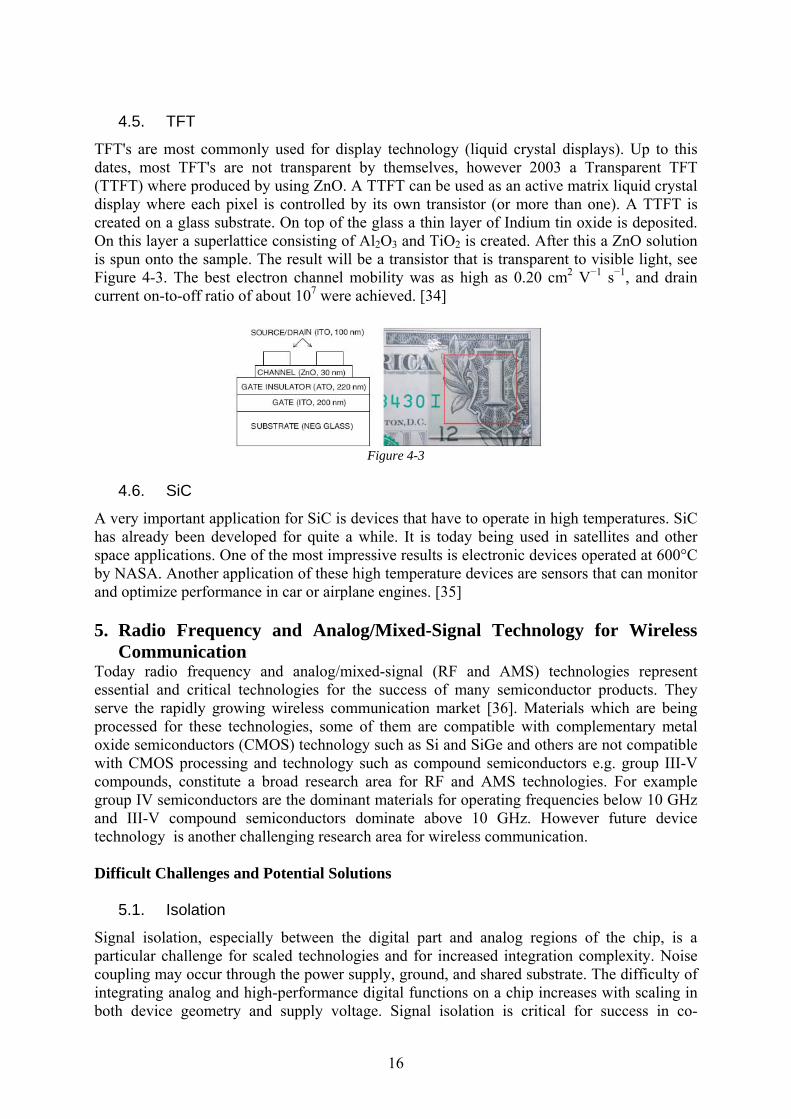
4.5. TFT
TFT's are most commonly used for display technology (liquid crystal displays). Up to this dates, most TFT's are not transparent by themselves, however 2003 a Transparent TFT (TTFT) where produced by using ZnO. A TTFT can be used as an active matrix liquid crystal display where each pixel is controlled by its own transistor (or more than one). A TTFT is created on a glass substrate. On top of the glass a thin layer of Indium tin oxide is deposited. On this layer a superlattice consisting of Al2O3 and TiO2 is created. After this a ZnO solution is spun onto the sample. The result will be a transistor that is transparent to visible light, see Figure 4-3. The best electron channel mobility was as high as 0.20 cm2 V−1 s−1, and drain current on-to-off ratio of about 107 were achieved. [34]
Figure 4-3
4.6. SiC
A very important application for SiC is devices that have to operate in high temperatures. SiC has already been developed for quite a while. It is today being used in satellites and other space applications. One of the most impressive results is electronic devices operated at 600°C by NASA. Another application of these high temperature devices are sensors that can monitor and optimize performance in car or airplane engines. [35] 5. Radio Frequency and Analog/Mixed-Signal Technology for Wireless
Communication Today radio frequency and analog/mixed-signal (RF and AMS) technologies represent essential and critical technologies for the success of many semiconductor products. They serve the rapidly growing wireless communication market [36]. Materials which are being processed for these technologies, some of them are compatible with complementary metal oxide semiconductors (CMOS) technology such as Si and SiGe and others are not compatible with CMOS processing and technology such as compound semiconductors e.g. group III-V compounds, constitute a broad research area for RF and AMS technologies. For example group IV semiconductors are the dominant materials for operating frequencies below 10 GHz and III-V compound semiconductors dominate above 10 GHz. However future device technology is another challenging research area for wireless communication. Difficult Challenges and Potential Solutions
5.1. Isolation
Signal isolation, especially between the digital part and analog regions of the chip, is a particular challenge for scaled technologies and for increased integration complexity. Noise coupling may occur through the power supply, ground, and shared substrate. The difficulty of integrating analog and high-performance digital functions on a chip increases with scaling in both device geometry and supply voltage. Signal isolation is critical for success in co-
16
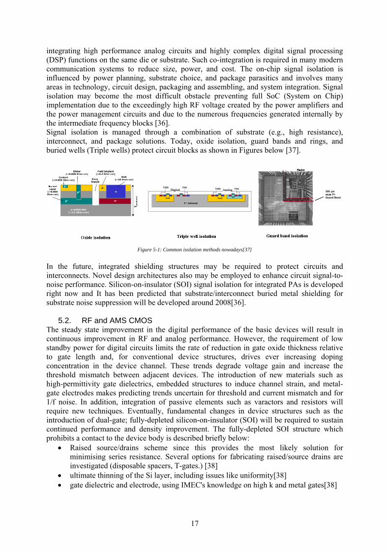
integrating high performance analog circuits and highly complex digital signal processing (DSP) functions on the same die or substrate. Such co-integration is required in many modern communication systems to reduce size, power, and cost. The on-chip signal isolation is influenced by power planning, substrate choice, and package parasitics and involves many areas in technology, circuit design, packaging and assembling, and system integration. Signal isolation may become the most difficult obstacle preventing full SoC (System on Chip) implementation due to the exceedingly high RF voltage created by the power amplifiers and the power management circuits and due to the numerous frequencies generated internally by the intermediate frequency blocks [36]. Signal isolation is managed through a combination of substrate (e.g., high resistance), interconnect, and package solutions. Today, oxide isolation, guard bands and rings, and buried wells (Triple wells) protect circuit blocks as shown in Figures below [37].
Figure 5-1: Common isolation methods nowadays[37]
In the future, integrated shielding structures may be required to protect circuits and interconnects. Novel design architectures also may be employed to enhance circuit signal-to-noise performance. Silicon-on-insulator (SOI) signal isolation for integrated PAs is developed right now and It has been predicted that substrate/interconnect buried metal shielding for substrate noise suppression will be developed around 2008[36].
5.2. RF and AMS CMOS The steady state improvement in the digital performance of the basic devices will result in continuous improvement in RF and analog performance. However, the requirement of low standby power for digital circuits limits the rate of reduction in gate oxide thickness relative to gate length and, for conventional device structures, drives ever increasing doping concentration in the device channel. These trends degrade voltage gain and increase the threshold mismatch between adjacent devices. The introduction of new materials such as high-permittivity gate dielectrics, embedded structures to induce channel strain, and metal-gate electrodes makes predicting trends uncertain for threshold and current mismatch and for 1/f noise. In addition, integration of passive elements such as varactors and resistors will require new techniques. Eventually, fundamental changes in device structures such as the introduction of dual-gate; fully-depleted silicon-on-insulator (SOI) will be required to sustain continued performance and density improvement. The fully-depleted SOI structure which prohibits a contact to the device body is described briefly below:
• Raised source/drains scheme since this provides the most likely solution for minimising series resistance. Several options for fabricating raised/source drains are investigated (disposable spacers, T-gates.) [38]
• ultimate thinning of the Si layer, including issues like uniformity[38] • gate dielectric and electrode, using IMEC's knowledge on high k and metal gates[38]
17
Figure 5-2: TEM cross-section of the FDSOI MOSFET with raised S/D scheme. [38] Thus, the electrical characteristics of these devices are different from that of conventional CMOS. Therefore, the fabrication of conventional precision analog and RF driver devices and resistors and varactors may require separate process steps with the attendant increase in die cost. Finally, the steady state reduction in analog supply voltage poses a significant circuit design challenge [36]. The introduction of metal gates may reduce threshold mismatch due to variations in gate doping and will increase Fmax due to decreased gate resistance. The introduction of channel strain to increase device current should enable improvements in precision analog and RF driver performance with little or no degradation in other characteristics. Fully-depleted, dual-gate SOI has low channel doping relative to conventional CMOS structures and so may have reduced mismatch. In addition, this structure will offer reduced drain conductance with an attendant increase in voltage-gain and Fmax. The multiple threshold voltages that enable optimization of digital power-delay will also offer design options for mixed-signal and RF applications[37].
5.3. RF and AMS bipolar devices Near-term challenges for BiCMOS technology include reducing the cost of BiCMOS technology while improving power and the increased difficulty with integrating bipolar devices in aggressively scaled CMOS due to conflicting thermal budget requirements. The major long-term challenge for BiCMOS technology includes enabling the scaling of bipolar power supply to reduce power consumption versus CMOS technology.
Figure 5-3: TEM picture of a SiGe BiCMOS device cross section [39]
18
Along with RFCMOS, SiGe has established itself as one of the key technologies of choice for cellular receivers. Its superior noise figure, gain characteristics, and state of the art 1/f noise properties allow extremely efficient and compact receiver block designs. Bipolar performance shows an aggressive roadmap for the Ft and Fmax improvement. This improvement will be accomplished up to an Ft of about 300 GHz for bipolar devices by techniques that continue to push both vertical and lateral scaling. Vertical scaling is likely to be accomplished with evolutionary improvement in current equipment and techniques and the addition of carbon doping. Beyond Ft of about 300 GHz, it is likely that more advanced epitaxial techniques will be required, such as atomic layer epitaxy. Beyond an Ft of about 400 GHz, it is likely that additional materials and dopants will need to be introduced. Lateral scaling will borrow heavily from techniques being adopted for digital CMOS and is not likely to add any more requirements than those for scaling of digital CMOS.
[2] “Transcending Moore’s Law with molecular electronics and nanotechnology”, 2004, www.dfj.com/files/TranscendingMoore.pdf
[3] http://www.ipt.arc.nasa.gov/Graphics/nanotech_nasamissions.pdf[4] http://www.mtmi.vu.lt/pfk/funkc_dariniai/nanostructures/molec_computer.htm[5] www.uaf.edu/chem/467Sp05/lecture15.PPT[6] S. Lai, Current status of the phase change memory and its future, International Electron Devices
Meeting, 2003-12-09. [7] S. Lai, T. Lowrey, OUM – A 180 nm Nonvolatile Memory Cell Element Technology For Stand Alone
and Embedded Applications, Proceedings of IEEE International Electron Devices Meeting (IEDM), 2001-12-05.
[8] M. Gill, T. Lowrey, J. Park, Ovonic Unified Memory – A High-performance Nonvolatile Memory Technology for Stand Alone Memory and Embedded Applications, Proceedings of 2002 IEEE International Solid State Circuits Conference, 2002-02-04.
[9] G. Atwood, A. Fazio, D. Mills, B. Reaves, Intel StrataFlashTM Memory Technology Overview, http://www.intel.com/technology/silicon/flash.htm, accessed 2006-05-10.
[10] A. Sheikholeslami, P. G. Gulak, A survey of circuit innovations in Ferroelectric random-access memories, Proceedings of the IEEE, Vol. 88, no. 3, pp. 667 – 689, 2005-05.
[11] International Technology Roadmap for Semiconductors, 2005 Edition, http://www.itrs.net/Common/2005ITRS/Home2005.htm, accessed 2006-05-10.
[12] J. Åkerman, Toward a Universal Memory, Science Magazine, Vol. 308, no. 5721, pp. 508 – 510, 2005-04-22.
[13] R. Butner, Computing Unplugged, http://www.research.ibm.com/thinkresearch/pages/2001/20010202_mram.shtml, accessed 2005-05-10.
1488-1495 [21] Technology Roadmap for Nanoelectronics, 1999 Edition,
http://cordis.europa.eu/esprit/src/melna-rm.htm [22] Jonker, B. T. et al., ”Electrical Spin Injection and Transport in Semiconductor Spintronic Devices”,
Mater. Res. Soc. Bull. 28 (2003) 740–748 [23] Rashba, E.I., ”Theory of electrical spin injection: Tunnel contacts as a solution of the conductivity
mismatch problem”, Phys. Rev. B. 62 (2000) R16267-R16270 [24] Oestreich M., "Injection of spin for electronics", Physics in Action, Physics World, p.23, August 2001 [25] International Technology Roadmap for Semiconductors, 2005 Edition,
http://www.itrs.net/Common/2005ITRS/Home2005.htm, accessed 2006-05-11. [26] Ohno, Y. et al., ”Electrical spin injection in a ferromagnetic semiconductor heterostructure”, Nature
402 (1999) 790-792 [27] Hanbicki, A.T. et al., ”Analysis of the transport process providing spin injection through
an Fe/AlGaAs Schottky barrier”, Appl. Phys. Lett. 82 (2003) 4092-4094 [28] 1. S. J. Pearton “GaN and related materials 2, Optoelectronic properties of semiconductors and
superlattices” ISBN 90-5699-685-1 (2000) [29] S.Yoshidaa, J. Suzuki “Reliability of metal semiconductor field-effect transistor
using GaN at high temperature” Journal of Applied Physics 84 , 2940 (1998) [30] Y. Chang, Y. Zhang, Y. Zhang, K.Y. Tong “A thermal model for static current characteristics of
AlGaN/GaN high electron mobility transistors including self-heating effect” Journal of Applied Physics 99, (2006)
[31] C. J. Kao, M.C Chen, C. J. Tun, G. C. Chi, J. K. Sheu, W. C. Lai, M. L. Lee, F. Ren, S. J. Pearton, “Comparison of low-temperature GaN, SiO2, and SiNx as gate insulators
on AlGaN/GaN heterostructure field-effect transistors” Journal of Applied Physics 98, (2005) [32] Gallium Nitride, http://en.wikipedia.org/wiki/GaN, accessed 2005-05-13. [33] Zinc Oxide http://en.wikipedia.org/wiki/ZnO, accessed 2005-05-13. [34] B. J. Norris, J. Anderson, J. F. Wager, D. A. Keszler, “Spin-coated zinc oxide transparent