57
Kelin Kuhn / IWCE / Beijing / 2009 1 Moore's Law past 32nm: Future Challenges in Device Scaling Kelin J. Kuhn Intel Fellow Director of Advanced Device Technology Intel Corporation

Kelin Kuhn / IWCE / Beijing / 2009 1
Moore's Law past 32nm: Future Challenges in Device Scaling
Kelin J. KuhnIntel Fellow
Director of Advanced Device Technology Intel Corporation

Kelin Kuhn / IWCE / Beijing / 2009 2
Agenda
• History• Architecture • Capacitance • Resistance • HiK-MG• Orientation• Strain• Strain + Orientation• Summary© 2009 Jupiterimages
Kelin Kuhn / IWCE / Beijing / 2009 3
Agenda
• History• Architecture • Capacitance • Resistance • HiK-MG• Orientation• Strain• Strain + Orientation• Summary© 2009 Jupiterimages
Kelin Kuhn / IWCE / Beijing / 2009 4
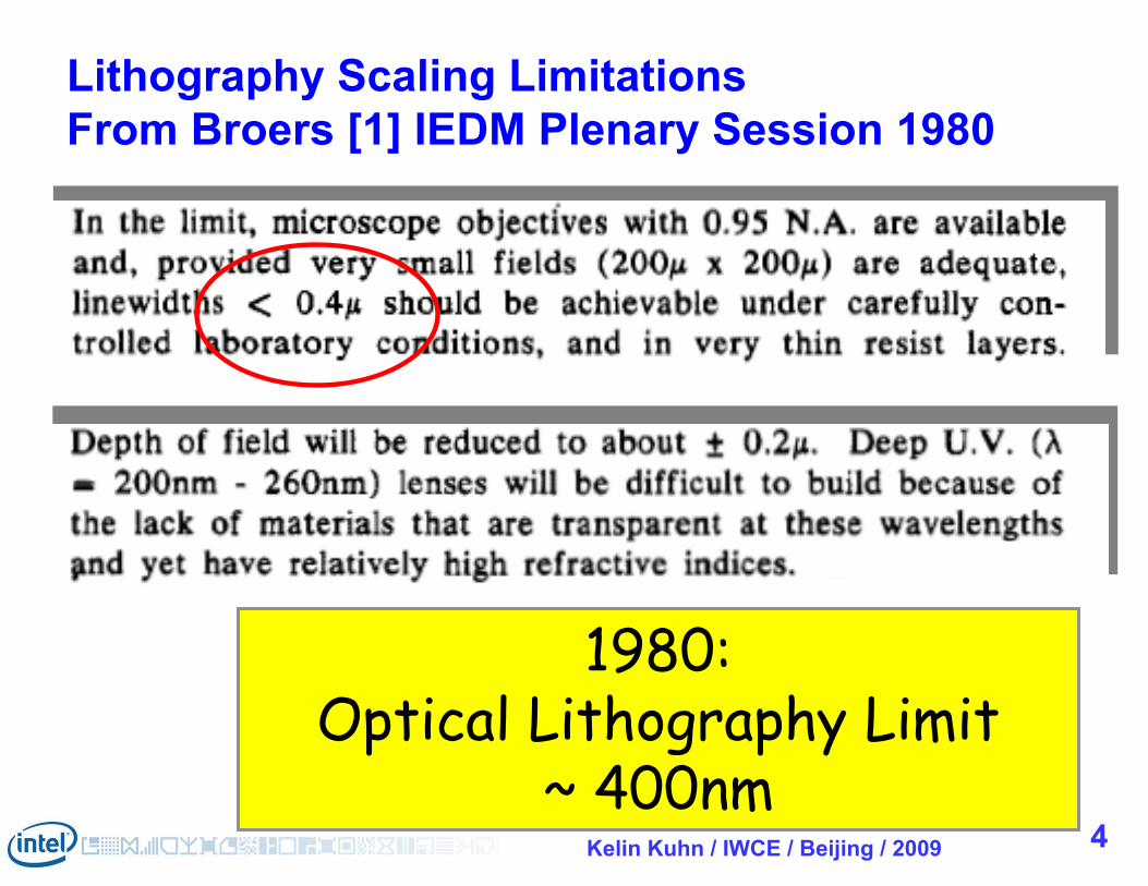
Lithography Scaling LimitationsFrom Broers [1] IEDM Plenary Session 1980
1980: Optical Lithography Limit
~ 400nm

Kelin Kuhn / IWCE / Beijing / 2009 5
Transistor Scaling LimitationsFrom Meindl [2] IEDM Plenary Session 1983
1983: Transistor architecture limit
200-400nm (SCE)

Kelin Kuhn / IWCE / Beijing / 2009 6
Transistor Scaling LimitationsFrom Heilmeier [4] IEDM Plenary Session 1984
1984: Transistor architecture limit300-500nm (laundry list of reasons…)

Kelin Kuhn / IWCE / Beijing / 2009 7
Moore’s Law Scaling
~300nm
~500nm
1983-84 limits on gate size, are commensurate with the dimensions
of 2008’s entire 32nm SRAM cell! 0.01
0.1
1
10
1970 1980 1990 2000 2010 2020
Mic
rons
45nm65nm
32nmFeature Size0.7x every 2 years
CPU Transistor Count2x every 2 years
103
105
109
107
Transistor dimensions scale to improve performance,reduce power, and reduce cost per transistor
Kelin Kuhn / IWCE / Beijing / 2009 8
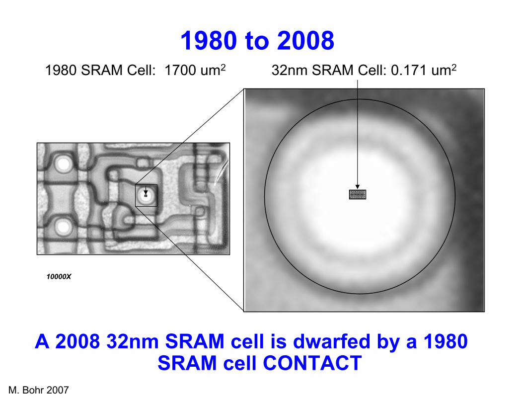
1980 SRAM Cell: 1700 um2 32nm SRAM Cell: 0.171 um2
M. Bohr 2007
A 2008 32nm SRAM cell is dwarfed by a 1980 SRAM cell CONTACT
1980 to 2008
10000X

Kelin Kuhn / IWCE / Beijing / 2009 9
Agenda
• History• Architecture• Capacitance • Resistance • HiK-MG• Orientation• Strain• Strain + Orientation• Summary© 2009 Jupiterimages

Kelin Kuhn / IWCE / Beijing / 2009 10
Planar Challenges
p+ poly
p+ ESD
p+ poly
p+ ESD
p+ poly
p+ ESD
Channel (Higher mobility channel arch.)
PMOS strain (Pitch scalable strain
solution)
Gate(SCE limitations)
Channel(Variation with high doping)
NMOS strain(Pitch scalable strain
solution)
Capacitance (Increased fringe to
contact/facet)
K. Kuhn – IEDM 2008
Kelin Kuhn / IWCE / Beijing / 2009 11
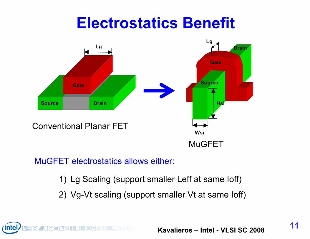
Electrostatics Benefit
1) Lg Scaling (support smaller Leff at same Ioff)
2) Vg-Vt scaling (support smaller Vt at same Ioff)
MuGFET electrostatics allows either:
Gate
Source Drain
Lg
Conventional Planar FET
Lg
Hsi
Gate
Source
Drain
Wsi
MuGFET
Kavalieros – Intel - VLSI SC 2008 [2]

Kelin Kuhn / IWCE / Beijing / 2009 12
Additional MuGFET Challenges
Rext: (Xj/Wsi
limitations)
Small fin pitch (2 generation scale?)
Fin/gate fidelity on 3’D(Patterning/etch) Gate wraparound
(Endcap coverage)
Topology(Polish / etch challenges)
Fin Strain engr.(Effective strain
transfer from a fin into the channel)
Variation(Mitigating RSD but acquiring Hsi/Wsi/epi)
Capacitance (Increased fringe to
contact/facet)
K. Kuhn – IEDM 2008

Kelin Kuhn / IWCE / Beijing / 2009 13
Agenda
• History• Architecture• Capacitance• Resistance • HiK-MG• Orientation• Strain• Strain + Orientation• Summary© 2009 Jupiterimages

Kelin Kuhn / IWCE / Beijing / 2009 14
Planar Capacitive Elements
Cjunction
Area junction
Gated-edge junction
Cfringe to Contact
Cfringe to facet
Cchannel componentof Cgate
Cxud - device component of Cov
(XUD-based)
Cfringe to diffusion (of/if)
K. Kuhn – IEDM 2008

Kelin Kuhn / IWCE / Beijing / 2009 15
Planar Capacitive Elements
Cfringe to Contact
“Golden” days of scaling:Who worried about Cfringe?
0%
5%
10%
15%
0 200 400GENERATION
PER
CEN
T C
FRIN
GE
PROCESS GENERATION (nm)
K. Kuhn – IEDM 2008K. Kuhn – IEDM 2008

Kelin Kuhn / IWCE / Beijing / 2009 16
Planar Capacitive Elements
Cfringe to Contact
Cfringe to facet
Cfringe to facet
“Silver” days of scaling: Introduction of epi:Increased fringe due to facet
0%
5%
10%
15%
0 200 400GENERATION
PER
CEN
T C
FRIN
GE
Epi facet
PROCESS GENERATION (nm)
K. Kuhn – IEDM 2008K. Kuhn – IEDM 2008

Kelin Kuhn / IWCE / Beijing / 2009 17
Planar Capacitive Elements
Cfringe to facet
Cfringe to Contact
“Bronze” days of scalingGate and contact CD dimensions scaling slower than
contacted gate pitch – fringe matters
0%
5%
10%
15%
0 200 400GENERATION
PER
CEN
T C
FRIN
GE
Reduced CON/GATE scale
PROCESS GENERATION (nm)
K. Kuhn – IEDM 2008K. Kuhn – IEDM 2008

Kelin Kuhn / IWCE / Beijing / 2009 18
Innovative Spacer Technologies
SPACER REMOVALLiow – NUS Singapore
EDL 2008 [11]
SiBCN (Low-K) SPACERKo –TSMC
VLSI 2008 [12]
37

Kelin Kuhn / IWCE / Beijing / 2009 19
Agenda
• History• Architecture• Capacitance• Resistance • HiK-MG• Orientation• Strain• Strain + Orientation• Summary© 2009 Jupiterimages

Kelin Kuhn / IWCE / Beijing / 2009 20
Planar Resistive Elements
RACCUMULATION
RSPREADING
REPI
RCONTACT
RINTERFACE
RSILICIDE
RACCUMULATION
RSPREADING
REPI
RCONTACT
RINTERFACE
RSILICIDE

Kelin Kuhn / IWCE / Beijing / 2009 21
Technology trends Xj/Tsi, Lg, Racc
ITRS 2007 [10]
05
101520253035
2000 2010 2020
TECHNOLOGY YEAR
XJ/ T
si(n
m),
Lga
te(n
m)
0%
10%
20%
30%
40%
IDEA
L R
acc/
(Vdd
/Idsa
t)
Lg
XJ “Tsi”
Rratio

Kelin Kuhn / IWCE / Beijing / 2009 22
Advanced Laser Anneal Technologies
Yamamoto – Fujitsu - IEDM 2007 [15]Multiple laser spikes + RTA
Ortolland – IMEC - VLSI 2008 [16]Non-melt LSA with adv. gate stacks
-0.8
-0.6
-0.4
-0.2
0
0.2
0.4
0.6
0.8
0.01 0.1 1Physical gate length [µm]
Vth
sat [
V] Spike onlyLaser only
nMOS
pMOS
FUSI
As 3KeV T15
B 0.5KeV T0
1.E-09
1.E-08
1.E-07
1.E-06
1.E-05
0 200 400 600Ion [µA/µm]
Ioff
[A/µ
m]
Spike onlyLow PowerMedium PowerHigh Power
pMOSFUSI
Laser Power Increase
FUSI RPG MIPSGate Last Gate last Gate first
@ L
DD
& H
alo
impl
ant s
tep
@ e
nd o
f pr
oces
s
poly
ALD - Metal
Metal footing

Kelin Kuhn / IWCE / Beijing / 2009 23
Low Barrier Height Contacts
.concdopingSubstrateND
)(SBHHeightBarrierSchottkyq B
• Limited additional improvement with Rsilicide(NiSi has the lowest known resistivity at 10.5 ohm-cm)
• SBH optimization has potential for Rinterface reduction
D
B
NqR expinterface
AR 1interface
areaContactA R ACCUMULATION
RSPREADING
REPI
RCONTACT
RINTERFACE
RSILICIDE

Kelin Kuhn / IWCE / Beijing / 2009 24
Schottky theory vs. experimental SBHs for metals on nSiMukherjee – Intel
nSi
(e.v
.)
Si Mid-Gap
0.1
0.1
0.3
0.5
0.7
0.9
1.1
1.3
1 2 3 4 5 6 7 8 9 10 11 12 13 14 15 16 17 18 19 20 21 22 23 24 25
Schottky theoryExperiment
Lanthanides
4th period transition metals
6th period transition metals
5th period transition metals
Ti22;4
V23;4
Cr24;4
Nb41;5
Zr40;5
Y39;5
Ni28;4
Co27;4Fe
26;4Mn25;4
Pt78;6
Ir77;6
Os76;4
Re75;6
W74;6
Ta73;6Hf
72;6
Er68;6
Dy66;6
Gd64;6
Pd46;5
Rh45;5Ru
44;5Mo42;5
Yb70;6
Desired for PMOS
Desired for NMOS
Fermi level pinned to mid-gap for most metals on Si
K. Kuhn – IEDM 2008

Kelin Kuhn / IWCE / Beijing / 2009 25
Lee –NUS-SingaporeIEDM 2006 [18]Ni-alloy silicides
Alloy and Implant Modifications to Silicides
Zhang – KTH SwedenEDL 2007 [20]
Implant modification of SBH(SB FET paper)
NiSiPtSi

Kelin Kuhn / IWCE / Beijing / 2009 26
Agenda
• History• Architecture• Capacitance• Resistance • HiK-MG• Orientation• Strain• Strain + Orientation• Summary© 2009 Jupiterimages

Kelin Kuhn / IWCE / Beijing / 2009 27
• High-k gate dielectric – Reduced gate leakage– Continued TOX scaling
• High-k gate dielectric – Reduced reliability– Reduced mobility
• Metal gates– Eliminate polysilicon depletion– Resolve VT pinning for high-k
gate dielectrics
• Metal gates– Dual bandedge workfunctions– Thermal stability– Process integration
BENEFITS CHALLENGES
High-k Metal Gate
Kelin Kuhn / IWCE / Beijing / 2009 28
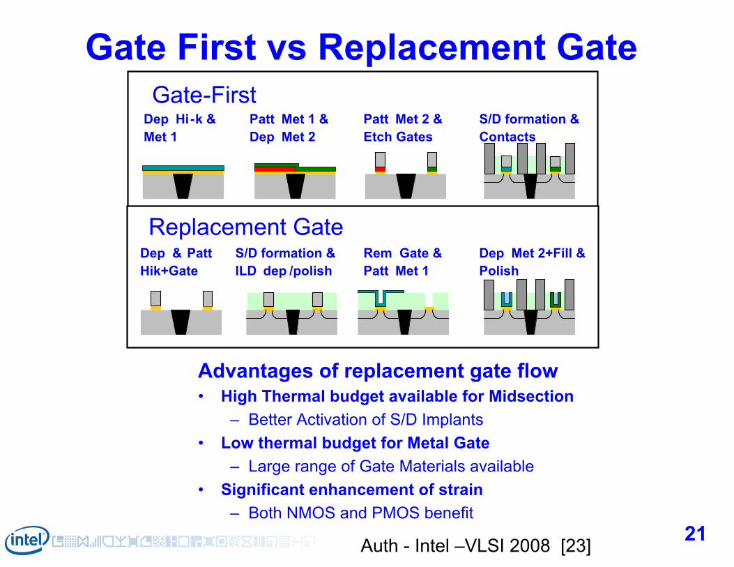
Gate First vs Replacement Gate
Advantages of replacement gate flow• High Thermal budget available for Midsection
– Better Activation of S/D Implants• Low thermal budget for Metal Gate
– Large range of Gate Materials available• Significant enhancement of strain
– Both NMOS and PMOS benefit
Gate-FirstDep Hi-k & Met 1
Patt Met 1 & Dep Met 2
Patt Met 2 & Etch Gates
S/D formation & Contacts
Dep & PattHik+Gate
S/D formation &ILD dep /polish
Rem Gate & Patt Met 1
Dep Met 2+Fill &Polish
Replacement Gate
21Auth - Intel –VLSI 2008 [23]

Kelin Kuhn / IWCE / Beijing / 2009 29
High-k/MG enables 0.7X ToxE scaling while reducing Ig > >25X for NMOS and 1000X for PMOS
65nm: Bai 2004 IEDM
0.00001
0.0001
0.001
0.01
0.1
1
10
100
-1.2 -0.8 -0.4 0 0.4 0.8 1.2
VGS (V)
Nor
mal
ized
Gat
e Le
akag
e
SiON/Poly 65nm
HiK+MG45nm
NMOS PMOS
HiK+MG45nm
SiON/Poly 65nm
Mistry - Intel - IEDM 2007 [8]
High-k Metal Gate: ToxE and Ig
Fanout = 2
3
4
5
6
7
8
9
10 100 1000 10000IOFFN + IOFFP (nA/um)
DEL
AY
PER
STA
GE
(pS)
65nm @ 1.2V
45nm @1.1V
FO=2 delay of 5.1 ps at IOFFN = IOFFP = 100 nA/mm 23% better than 65 nm at the same leakage and 100mV lower Vcc.

Kelin Kuhn / IWCE / Beijing / 2009 30
32nm Transistor Performance vs. Gate Pitch
Highest reported drive current at tightest reported gate pitchSimultaneous performance and density improvement [9]
90nm: Mistry, 2004 VLSI65nm: Tyagi, 2005 IEDM45nm: Mistry, 2007 IEDM32nm: Natarajan, 2008 IEDM
1001000 Contacted Gate Pitch (nm)
IDSA
T (m
A/u
m)
0.0
0.2
0.4
0.6
0.8
1.0
1.2
1.4
1.6
PMOS
160nm (45nm)
220nm (65nm)
320nm (90nm)
1.0V, 100 nA/m
Gate Pitch (Generation)
112.5nm (32nm)
1001000
IDSA
T (m
A/u
m)
0.4
0.6
0.8
1.0
1.2
1.4
1.6
PMOS
NMOS
160nm (45nm)
220nm (65nm)
320nm (90nm)
1.0V, 100 nA/m
Gate Pitch (Generation)
112.5nm (32nm)

Kelin Kuhn / IWCE / Beijing / 2009
FOUR GENERATION COMPARISON
45nm: 1st gen. HiK-MG [8]
32nm:2nd gen. HiK-MG [9]
1
10
100
1000
0.4 0.5 0.6 0.7 0.8 0.9 1.0 1.1 1.2 1.3
90 nm
1.4 1.5 1.6
1 1.2 1.4 1.61
10
100
1000
0.8 0.9 1.1 1.3 1.5 1.8 2.01.7 1.9
65 nm
90 nm
NMOS Ion-Ioff Vdd=1.0V
Idsat (mA/um)
Ioff
(nA
/um
)Io
ff( n
A/u
m)
45 nm1st Hi-K MG
PMOS Ion-Ioff Vdd=1.0V
65 nm
32 nm2nd Hi-K MG
45 nm1st Hi-K MG
32 nm2nd Hi-K MG

Kelin Kuhn / IWCE / Beijing / 2009 32
Agenda
• History• Architecture• Capacitance• Resistance • HiK-MG• Orientation• Strain• Strain + Orientation• Summary© 2009 Jupiterimages

Kelin Kuhn / IWCE / Beijing / 2009 33
(110) surface – top down(100) surface – top down
HH
Non-standard
(110) Surface
Three possible channel directions<110> <111> and <100>
<110>
<110>
<100>
(100)
<100>
<110>
<111>
(110)
MASTAR [46]
<100>
Standard wafer / direction(100) Surface / <110> channel
(100) Surface / <100> (a “45 degree” wafer)
Both <110> directions are the same.
<110>
<100>
<110>
<111>
<110>
LengthLength

Kelin Kuhn / IWCE / Beijing / 2009 34
OVERALL BEST? (100) and (110) comparisons (no strain)NMOS (100) <110>, PMOS (110) <110>
Chang - IBMTED 2004 [26]
Yang – AMD/IBM EDST 2007 [27]
Sato [25]Phys. Rev. (1971)
elec
tron
hole

Kelin Kuhn / IWCE / Beijing / 2009 35
Put NMOS at 45degrees to
PMOS?
(110) Surface
PMOS VERTICAL DEVICES on (100)
(110) surface <110> channel results when a VFET is fabricated on typical (100) Si - good for PMOS, not for NMOS
<110> channel
Chang - IBM –TED 2004 [54]
Put NMOS at 45degrees to
PMOS?
(110) Surface
PMOS VERTICAL DEVICES on (100)
(110) surface <110> channel results when a VFET is fabricated on typical (100) Si - good for PMOS, not for NMOS
<110> channel
Chang - IBM –TED 2004 [54]

Kelin Kuhn / IWCE / Beijing / 2009 36
Put NMOS at 45degrees to
PMOS?Put NMOS at 45degrees to
PMOS?
NMOS VERTICAL DEVICES on (100)
(100) Surface
Put NMOS at 45degrees to
PMOS?Put NMOS at 45degrees to
PMOS?
NMOS VERTICAL DEVICES on (100)
(100) Surface
(100) surface <100> channel for a VFET fabricated at 45 degrees typical (100) Si – very challenging for lithography at 22nm node
(100) surface <100> channel for a VFET fabricated at 45 degrees typical (100) Si – very challenging for lithography at 22nm node
<100> channel
Chang - Berkeley Proc. IEEE 2003 [56]
<100> channel
Chang - Berkeley Proc. IEEE 2003 [26]

Kelin Kuhn / IWCE / Beijing / 2009 37
Early HOT
Yang – IBMIEDM 2003 [27]
First HOT
Yang – AMD/IBMVLSI 2004HOT RO
IoffN + IoffP (A)
Elegant solution!
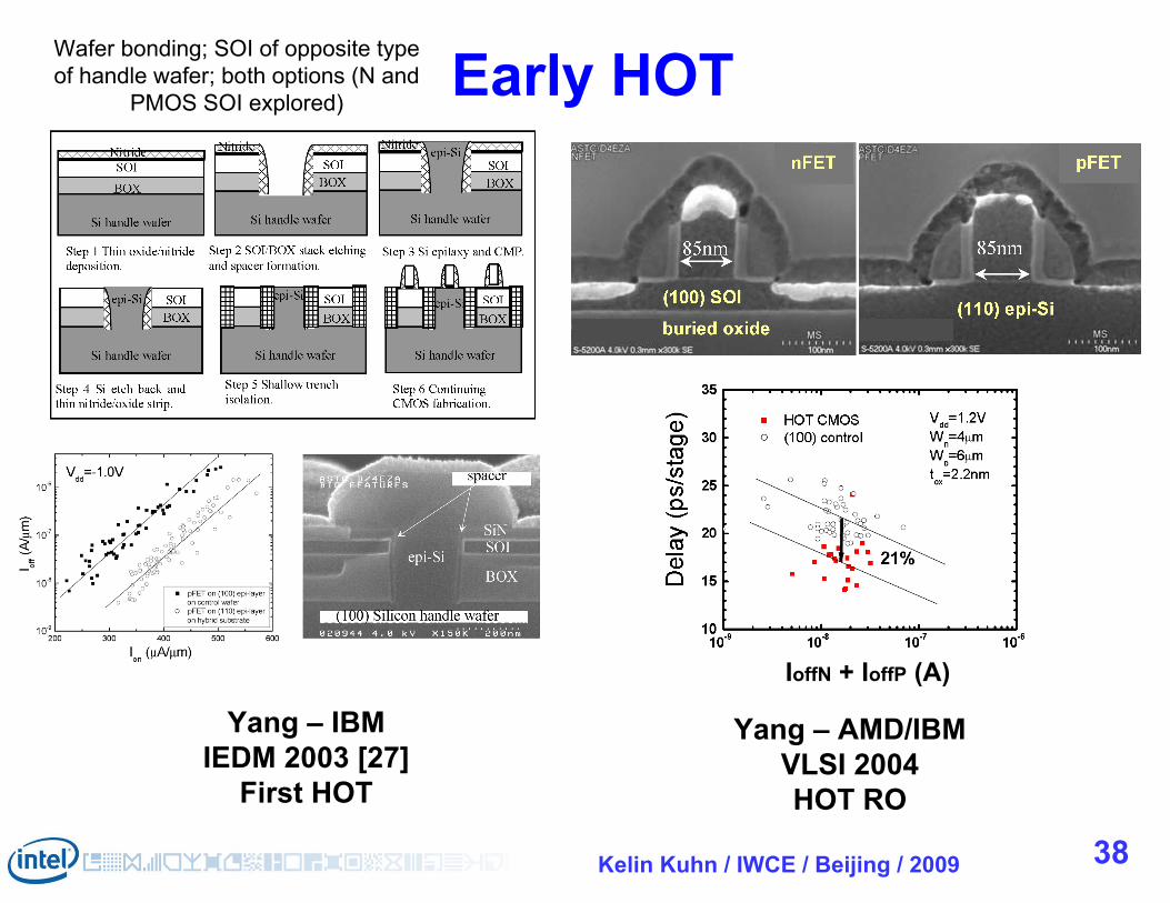
Kelin Kuhn / IWCE / Beijing / 2009 38
Early HOT
Yang – IBMIEDM 2003 [27]
First HOT
IoffN + IoffP (A)
Wafer bonding; SOI of opposite type of handle wafer; both options (N and
PMOS SOI explored)
Yang – AMD/IBMVLSI 2004HOT RO

Kelin Kuhn / IWCE / Beijing / 2009 39
HOT architecture options
Sung – IBMIEDM 2005 [28]
Direct silicon-bond HOT
Yang – IBM VLSI 2006 [29]~Dual SOI HOT
SuperHot

Kelin Kuhn / IWCE / Beijing / 2009 40
Agenda
• History• Architecture• Capacitance• Resistance • HiK-MG• Orientation• Strain• Strain + Orientation• Summary© 2009 Jupiterimages

Kelin Kuhn / IWCE / Beijing / 2009 41
Strain: Importance in scaling
Strain (first introduced at 90nm) is a critical ingredient in modern transistor scaling
130nm 90nm 65nm 45nm 32nm
PMOS
Cha
nnel
str
ain

Kelin Kuhn / IWCE / Beijing / 2009 42
Electron mobility enhancement: Biaxial
Welser – Stanford IEDM 1992/1994 [30]
Strained Si/Relaxed SiGe
Hoyt – MITIEDM 2002 [31]
Strained Si/Relaxed SiGe
Rim – IBMVLSI 2002 [32]
Strained Si/Relaxed SiGe
SiO2Drain Source
Relaxed Si0.7 Ge0.3
Strained Si
Relaxed Graded Si1-yGey layer y = 0 to 0.3
n+ n+100 Å
1 µm
n+ poly
~~ ~~
Si substrate
0.80
1.0
1.2
1.4
1.6
1.8
2.0
0.0 0.10 0.20 0.30 0.40
Welser IEDM '94
Tezuka, VLSI '02
Rim, VLSI '01Currie, 2001 [14]
Welser IEDM '92
Mob
ility
enha
ncem
ent r
atio
Substrate Ge fraction, x
Calc. for strained Si (phonon-limited)
0.80
1.0
1.2
1.4
1.6
1.8
2.0
0.0 0.10 0.20 0.30 0.400.80
1.0
1.2
1.4
1.6
1.8
2.0
0.0 0.10 0.20 0.30 0.40
Welser IEDM '94
Tezuka, VLSI '02
Rim, VLSI '01Currie, 2001 [14]
Welser IEDM '92
Mob
ility
enha
ncem
ent r
atio
Substrate Ge fraction, x
Calc. for strained Si (phonon-limited)

Kelin Kuhn / IWCE / Beijing / 2009 43
Electron mobility enhancement: Biaxial
Welser – Stanford IEDM 1992/1994 [30]
Strained Si/Relaxed SiGe
Hoyt – MITIEDM 2002 [31]
Strained Si/Relaxed SiGe
Rim – IBMVLSI 2002 [32]
Strained Si/Relaxed SiGe
SiO2Drain Source
Relaxed Si0.7 Ge0.3
Strained Si
Relaxed Graded Si1-yGey layer y = 0 to 0.3
n+ n+100 Å
1 µm
n+ poly
~~ ~~
Si substrate
Exploring and controlling the lower VT associated with
short channel strained NMOS
Further quantifying the strain enhancement, including
vertical effective field and doping
Kelin Kuhn / IWCE / Beijing / 2009 44
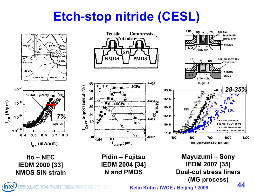
Etch-stop nitride (CESL)
Mayuzumi – SonyIEDM 2007 [35]
Dual-cut stress liners(MG process)
28-35%
Pidin – FujitsuIEDM 2004 [34]N and PMOS
Ito – NECIEDM 2000 [33]
NMOS SiN strain
7%

Kelin Kuhn / IWCE / Beijing / 2009 45
Thompson – IntelIEDM 2002 / 2004 [6]
Ghani – Intel IEDM 2003 [36]
ChidambaramTI / Applied Materials
VLSI - 2004 [37]
Embedded SiGe (PMOS)

Kelin Kuhn / IWCE / Beijing / 2009 46
Embedded SiGe (PMOS)
Ohta – FujitsuIEDM 2005 [39]
Profile engr.
Zhang – FreescaleVLSI 2005 [40]Thin body SOI
Lee - IBMIEDM 2005 [38]SOI and e-SiGe
~20%
~14% RO delay

Kelin Kuhn / IWCE / Beijing / 2009 47
Enhanced PMOS strain: Gate last HiK-MG
Auth – Intel VLSI 2008 [23]
Before gate removal After gate removal
Wang – SonyVLSI 2007 [41]
14% RMG

Kelin Kuhn / IWCE / Beijing / 2009 48
Stress Memorization (SMT)
Ota – MitsubishiIEDM 2002 [42]
NMOS SMT
Chen – TSMC VLSI 2004 [43]
NMOS SMT
Wei – AMDVLSI 2007 [44]Multiple liners
>27%
11-15%

Kelin Kuhn / IWCE / Beijing / 2009 49
SMT enhancement with HiK-MGKubicek – IMEC – VLSI 2008 [45]
From the paper: “… the gain from traditional stress boosters (CESL,
embedded-SiGe, channel orientation) was maintained on High-κ/Metal gate..”

Kelin Kuhn / IWCE / Beijing / 2009 50
Embedded Si:C (NMOS)
Yang –IBM IEDM 2008
In-situ epi P-SiC
Liu – IBMVLSI 2007 [47]Implant + SPE
Ang – NUS-SingaporeIEDM 2004 [46]
Selective epi SiC (undoped)
~9% from SiC
6% from SiC

Kelin Kuhn / IWCE / Beijing / 2009 51
Metal stress (gate and contact)
Auth – IntelVLSI 2008 [23]
Kang – SematechIEDM 2006 [49]
NMOS PMOS
Different gate stack Raised S/D
+10%
1
10
100
1000
0.70 0.90 1.10 1.30Idsat(mA/m)
Ioff
(nA
/m
)
Tensile ContactControl
VDD = 1.0V
+10%
1
10
100
1000
0.70 0.90 1.10 1.30Idsat(mA/m)Idsat(mA
+5%
1
10
100
1000
0.9 1.1 1.3 1.5Idsat(mA/m)
Ioff
(nA
/m
)
Compressive GateControl
VDD = 1.0V
+5%
1
10
100
1000
0.9 1.1 1.3 1.5Idsat(mA
5.4-6.5%

Kelin Kuhn / IWCE / Beijing / 2009 52
• History• Architecture• Capacitance• Resistance • HiK-MG• Orientation• Strain• Strain + Orientation• Summary
Agenda
© 2009 Jupiterimages

Kelin Kuhn / IWCE / Beijing / 2009 53
Strain and OrientationPiezoresistive coefficient as a function of direction
NMOS PMOS
Udo – Infineon – Proc. IEEE Sensors 2004

Kelin Kuhn / IWCE / Beijing / 2009 54
Krishnamohan – Stanford – IEDM 2008
Kelin Kuhn / IWCE / Beijing / 2009 55
Agenda
• History• Architecture• Capacitance• Resistance • HiK-MG• Orientation• Strain• Strain + Orientation• Summary© 2009 Jupiterimages

Kelin Kuhn / IWCE / Beijing / 2009 56
“Looking in the Crystal Ball”
Low risk – evolutionary change – large suite of proven successful options
Further enhancements in strain technology
High risk – significant challenges with parasitic R, parasitic C and strain
MuGFETs
Medium-high risk – low-k FE dielectrics pose significant process challenges
Reduction in MOS parasitic capacitance
Medium risk – new annealing technologies, RE/NM silicide options
Reduction in MOS parasitic resistance
Medium risk – requires some solution to the (100)<110>N vs (110)/<110>P issue
Optimized substrate and channel orientation
Low risk – continual improvement – driven by strong research/development efforts
Further enhancements in HiK-MG technology
COMMENTSCHANGE

Kelin Kuhn / IWCE / Beijing / 2009 57
Q&A
© 2009 Jupiterimages


![Introduction NXDN IWCE 2019 FINAL.ppt [互換モード] 201… · Title: Microsoft PowerPoint - Introduction_NXDN_IWCE 2019_FINAL.ppt [互換モード] Author: i34096 Created Date:](https://static.documents.pub/doc/80x56/5fa66aa332c9481a2b166c53/introduction-nxdn-iwce-2019-finalppt-fff-201-title-microsoft-powerpoint.jpg)


