Page 1
FYS3410 - Vår 2014 (Kondenserte fasers fysikk) http://www.uio.no/studier/emner/matnat/fys/FYS3410/v14/index.html
Pensum: Solid State Physics by Philip Hofmann (Chapters 1-7 and 11)
Andrej Kuznetsov
delivery address: Department of Physics, PB 1048 Blindern, 0316 OSLO
Tel: +47-22857762,
e-post: [email protected]
visiting address: MiNaLab, Gaustadaleen 23c
Page 2
Lecture schedule (based on P.Hofmann’s Solid State Physics,chapters 1-7 and 11)
Module I – Periodic Structures and Defects 20/1 Introduction. Crystal bonding. Periodicity and lattices, reciprocal space 4h
21/1 Laue condition, Ewald construction, interpretation of a diffraction experimen 2h
22/1 Bragg planes and Brillouin zones (BZ) 2h
23/1 Elastic strain and structural defects 2h
23/1 Atomic diffusion and summary of Module I 2h
Module II - Phonons 03/2 Vibrations, phonons, density of states, and Planck distribution 4h
04/2 Lattice heat capacity: Dulong-Petit, Einstien and Debye models 2h
05/2 Comparison of different models 2h
06/2 Thermal conductivity 2h
07/2 Thermal expansion and summary of Module II 2h
Module III – Electrons 24/2 Free electron gas (FEG) versus Free electron Fermi gas (FEFG) 4h
25/2 Effect of temperature – Fermi- Dirac distribution 2h
26/2 FEFG in 2D and 1D, and DOS in nanostructures 2h
27/2 Origin of the band gap and nearly free electron model 2h
28/2 Number of orbitals in a band and general form of the electronic states 2h
Module IV – Semiconductors 10/3 Energy bands and effective mass method 4h
11/3 Density of states in 3D semiconductors and nanostructures 2h
12/3 Intrinsic semiconductors 2h
13/3 Impurity states in semiconductors and carrier statistics 2h
14/3 p-n junctions and optoelectronic devices 2h
Page 3
Lecture 18: Energy bands in solids
• Bloch theorem
• Kronig-Penney model
• Empty lattice approximation
• Number of states in a band and filing of the bands
• Interpretation of the effective mass
• Effective mass method for hydrogen-like impurities
Page 4
Lecture 18: Energy bands in solids
• Origin of the band gap and Bloch theorem
• Kronig-Penney model
• Empty lattice approximation
• Number of states in a band and filing of the bands
• Interpretation of the effective mass
• Effective mass method for hydrogen-like impurities
Page 5
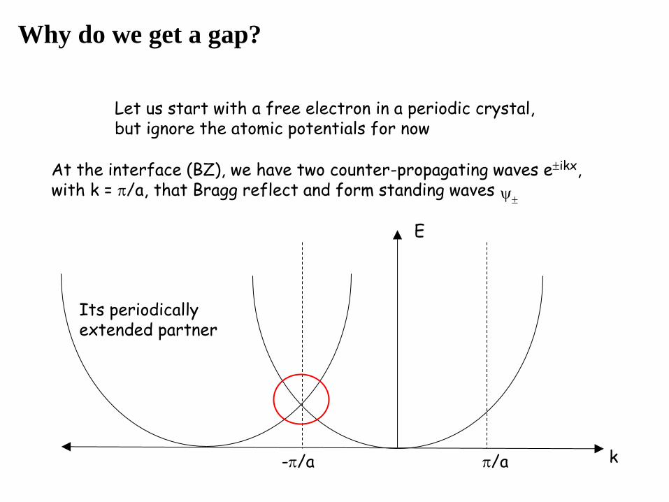
Why do we get a gap?
E
k p/a -p/a
At the interface (BZ), we have two counter-propagating waves eikx, with k = p/a, that Bragg reflect and form standing waves y
Its periodically extended partner
Let us start with a free electron in a periodic crystal, but ignore the atomic potentials for now
Page 6
Why do we get a gap?
E
k p/a -p/a
y- y+
Its periodically extended partner
y+ ~ cos(px/a) peaks at atomic sites
y- ~ sin(px/a) peaks in between
Page 7
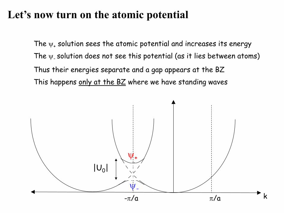
Let’s now turn on the atomic potential
The y+ solution sees the atomic potential and increases its energy
The y- solution does not see this potential (as it lies between atoms)
Thus their energies separate and a gap appears at the BZ
k p/a -p/a
y+
y-
|U0|
This happens only at the BZ where we have standing waves
Page 8
Bloch theorem
If V(r) is periodic with the periodicity of the lattice, then
the solutions of the one-electron Schrödinger eq.
Where uk(r) is periodic with the periodicity of the direct lattice.
uk(r) = uk(r+T); T is the translation vector of lattice.
“ The eigenfunctions of the wave equation for a periodic potential
are the product of a plane wave exp(ik·r) times a function uk(r)
with the periodicity of the crystal lattice.”
Page 9
Lecture 18: Energy bands in solids
• Origin of the band gap and Bloch theorem
• Kronig-Penney model
• Empty lattice approximation
• Number of states in a band and filing of the bands
• Interpretation of the effective mass
• Effective mass method for hydrogen-like impurities
Page 10
• Kronig and Penney assumed that an electron
experiences an infinite one-dimensional array of finite
potential wells.
• Each potential well models attraction to an atom in the
lattice, so the size of the wells must correspond roughly
to the lattice spacing.
Kronig-Penney Model
Page 11
• An effective way to understand the energy gap in
semiconductors is to model the interaction between
the electrons and the lattice of atoms.
• R. de L. Kronig and W. G. Penney developed a
useful one-dimensional model of the electron lattice
interaction in 1931.
Kronig-Penney Model
Page 12
• Since the electrons are not free their energies are less
than the height V0 of each of the potentials, but the
electron is essentially free in the gap 0 < x < a, where
it has a wave function of the form
where the wave number k is given by the usual
relation:
Kronig-Penney Model
Page 13
• In the region between a < x < a + b the electron can
tunnel through and the wave function loses its
oscillatory solution and becomes exponential:
Kronig-Penney Model
Page 14
• The left-hand side is limited to values between +1 and
−1 for all values of K.
• Plotting this it is observed there exist restricted (shaded)
forbidden zones for solutions.
Kronig-Penney Model
Page 15
• Matching solutions at the boundary, Kronig and
Penney find
Here K is another wave number. Let’s label the
equation above as KPE – Kronig-Penney equation
Kronig-Penney Model
Page 16
(a) Plot of the left side of Equation
(KPE) versus ka for κ2ba / 2 = 3π / 2.
Allowed energy values must
correspond to the values of k for
for which the plotted
function lies between -1 and +1.
Forbidden values are shaded in light
blue.
(b) The corresponding plot of energy
versus ka for κ2ba / 2 = 3π / 2, showing
the forbidden energy zones (gaps).
Kronig-Penney Model
Page 17
Lecture 18: Energy bands in solids
• Origin of the band gap and Bloch theorem
• Kronig-Penney model
• Empty lattice approximation
• Number of states in a band and filing of the bands
• Interpretation of the effective mass
• Effective mass method for hydrogen-like impurities
Page 18
Suppose that we have empty lattice where the periodic
V(x)=0. Then the e-s in the lattice are free, so that
Empty lattice approximation
Page 19
in 3-dim.
Empty lattice approximation
Page 20
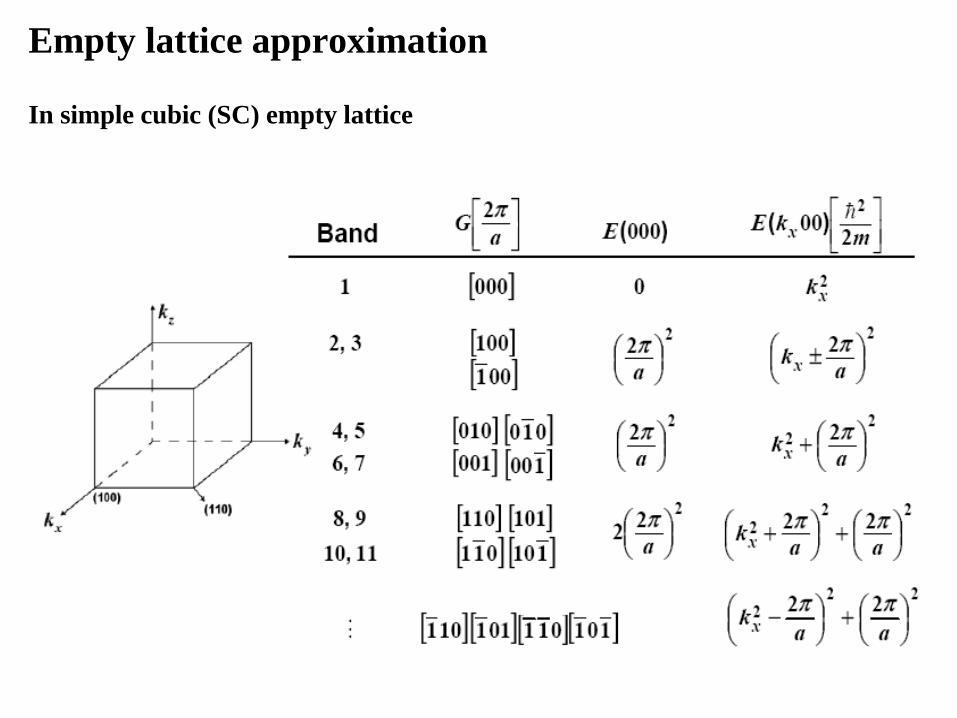
In simple cubic (SC) empty lattice
Empty lattice approximation
Page 21
Everything can be described
within the 1st B.Z.
Empty lattice approximation
Page 22
Lecture 18: Energy bands in solids
• Origin of the band gap and Bloch theorem
• Kronig-Penney model
• Empty lattice approximation
• Number of states in a band and filing of the bands
• Interpretation of the effective mass
• Effective mass method for hydrogen-like impurities
Page 23
k →
E
→
d
p
E
→
d
p2
[100] [110]
k →
Effective gap
o90Sin dk
p
p
Sin d
nk
o45Sin dk
p
Number of states in a band
Page 24
Monovalent metals
Divalent metals
Monovalent metals: Ag, Cu, Au → 1 e in the outermost orbital
outermost energy band is only half filled
Divalent metals: Mg, Be → overlapping conduction and valence bands
they conduct even if the valence band is full
Trivalent metals: Al → similar to monovalent metals!!!
outermost energy band is only half filled !!!
Filing of the bands
Page 25
SEMICONDUCTORS and ISOLATORS
Band gap
Elements of the 4th column (C, Si, Ge, Sn, Pb) → valence band full but no
overlap of valence and conduction bands
Diamond → PE as strong function of the position in the crystal
Band gap is 5.4 eV
Down the 4th column the outermost orbital is farther away from the nucleus
and less bound the electron is less strong a function of the position
in the crystal reducing band gap down the column
Filing of the bands
Page 26
Multiple Quantum Wells (MQWs) for advanced LEDs
MQWs
Single quantum well - repetitions of
ZnO/ZnCdO/ZnO periods
Page 27
Lecture 18: Energy bands in solids
• Origin of the band gap and Bloch theorem
• Kronig-Penney model
• Empty lattice approximation
• Number of states in a band and filing of the bands
• Interpretation of the effective mass
• Effective mass method for hydrogen-like impurities
Page 28
• The electron is subject to internal forces from the
lattice (ions and core electrons) AND external forces
such as electric fields
• In a crystal lattice, the net force may be opposite the
external force, however:
+ + + + +
Ep(x)
-
Fext =-qE
Fint =-dEp/dx
Internal and external forces affecting an electron in crystal
Page 29
• electron acceleration is not equal to Fext/me, but rather…
• a = (Fext + Fint)/me == Fext/m*
• The dispersion relation E(K) compensates for the internal
forces due to the crystal and allows us to use classical
concepts for the electron as long as its mass is taken as m*
+ + + + +
Ep(x)
-
Fext =-qE
Fint =-dEp/dx
Internal and external forces affecting an electron in crystal
Page 30
Hole - an electron near the top of an energy band
• The hole can be understood as an electron with negative effective mass
• An electron near the top of an energy band will have a negative effective mass
• A negatively charged particle with a negative mass will be accelerated like a positive particle with a positive mass (a hole!)
p/a
E(K)
K
F = m*a = QE
Without the crystal lattice, the hole would not exist!
The hole is a pure consequence of the periodic potential
operating in the crystal!!!
Page 31
E(K) and E(x)
p/a
E(K)
K
conduction band
valence band
EC
EV +
-
x
E(x)
Eg
Page 32
Generation and Recombination of electron-hole pairs
conduction band
valence band
EC
EV +
-
x
E(x)
+
-
Page 33
MQWs
Single quantum well - repetitions of
ZnO/ZnCdO/ZnO periods
Generation and Recombination of electron-hole pairs
Page 34
a
b
x
y
p/a
E(Kx)
Kx
p/b
E(Ky)
Ky
Different lattice spacings lead to different curvatures for E(K)
and effective masses that depend on the direction of motion.
Real 3D lattices, e.g. FCC, BCC, diamond, etc.
Page 35
light m*
(larger d2E/dK2)
heavy m*
(smaller d2E/dK2)
Real 3D lattices, e.g. FCC, BCC, diamond, etc.
21
, 2
1c ij
i j
Em
k k
Page 36
Real 3D lattices, e.g. FCC, BCC, diamond, etc.
Ge
Si
GaAs
Page 37
• energy (E) and momentum (ħK) must be conserved
• energy is released when a quasi-free electron recombines with a hole in the valence band:
ΔE = Eg
– does this energy produce light (photon) or heat (phonon)?
• indirect bandgap: ΔK is large
– but for a direct bandgap: ΔK=0
• photons have very low momentum
– but lattice vibrations (heat, phonons) have large momentum
• Conclusion: recombination (e-+h+) creates
– light in direct bandgap materials (GaAs, GaN, etc)
– heat in indirect bandgap materials (Si, Ge)
Direct and inderect band gap in semiconductors
Page 38
Motion of free electrons
0 d d
mdt dt
p r
F p
0
E E E E Eˆ ˆ ˆ ˆˆ ˆ x
x x y z
x x y z
pv v x v y v z x y z
m p p p p
v =
p
px
E(p) Consider free electron
0
Dispersion relation
Newton’s law of motion
2 2 21
0 2 2 2
E E E=
x y z
mp p p
2 2 2 2
0 0 0E / 2 =( + + ) / 2 x y zp m p p p m m p v
Velocity
Mass
Page 39
Effective mass
23
0 02, 1
31
, 0
, 1
1( ) ( )( ) ...
2
1... ( )
2
g i i j j
i j i j
g c ij i j i i i
i j
EE E k k k k
k k
E m p p p k k
k
E
ky
kx
k0
C.B. minimum
kox
koy
23
0 0
, 1
1( ) ( )( ) ...
2g i i j j
i j i j
EE E k k k k
k k
k
Taylor series near CB minimum
Effective mass tensor 2
1
, 2
1c ij
i j
Em
k k
Page 40
Density of states
kx
kz
ky
Parallelepiped of Volume V=LxLyLz
Allowed states satisfy boundary conditions: 2i i ik L np
Each state occupies volume in k space
3 3 18 /( ) 8k x y zV L L L V p p
Consider a conduction valley along x or [100] direction
2 22 2 2 2
( )2 2 2
yx zg
L T T
kk kE k E
m m m
2 22 2 2 2
12 ( ) 2 ( ) 2 ( )
yx z
L g T g T g
kk k
m E E m E E m E E
2 2 2
2 ( ) 2 ( ) 2 ( ), = , = ;
L g T g T g
x y z
m E E m E E m E Ea a a
Half axes
The volume in k-space containing energies less than E
3/ 2
1/ 2 3/ 2
2
4 4 2( ) ( )
3 3k x y z L T gV E a a a m m E Ep p
Page 41
Density of states
kx
kz
ky
3/ 2
1/ 2 3/ 2
2
4 2( ) ( )
3k L T gV E m m E Ep
3/ 2
1/ 2 3/ 2
2 2
2( ) 2 ( ) / ( )
3k k L T c
VN E V E V m m E E
p
Number of states with energies less than E
Multiply by number of valleys -G , divide by volume take derivative
3/ 23/ 2 *1 1/ 2 1/ 2 1/ 2
2 2 2 2
2( ) 2 1( ) ( ) ( )
2 2
nc L T g g
mN E Gg E G V m m E E E E
E p p
Number of states per unit volume per unit energy –density of states
Effective D.O.S. mass 1/3
* 2/3 2
n L Tm G m m
In GaAs *
n cm m
Page 42
Density of states in the valence band
k
E
3/ 23/ 23/ 2 **1/ 2 1/ 2 1/ 2
2 2 2 2 2 2
22 21 1 1( ) ( ) ( )
2 2 2
plh hhv lh hh
mm mg E g E g E E E E
p p p
Count energy down
Effective D.O.S. mass is 2/3
* 3/ 2 3/ 2 ~p hh lh hhm m m m
Page 43
Lecture 18: Energy bands in periodic crystalls
• Origin of the band gap and Bloch theorem
• Kronig-Penney model
• Empty lattice approximation
• Number of states in a band and filing of the bands
• Interpretation of the effective mass
• Effective mass method for hydrogen-like impurities in semiconductors
Page 44
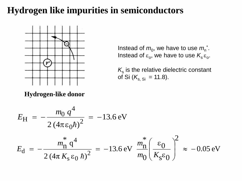
Hydrogen like impurities in semiconductors
d
Hydrogen-like donor Hydrogen atom
P donor in Si can be modeled as hydrogen-like atom
Page 45
Hydrogen atom - Bohr model
222
0
42
2
0
2
0
22
0
2
2
0
2
2
0
2
22
0
22
0
2
0
2
0
2
2
2
2
0
1
2)4(
2)4( :energy Total
242
1 :energy Kinetic
44 :energy Potential
4
1
4
4)(44
...3,2,1 ,for 4
1
n
emZEK
r
ZeVKE
r
ZemvK
r
Zedr
r
ZeV
n
Ze
mr
nv
mZe
nr
mr
n
mr
nmrrmvZe
nnmvrLr
vm
r
Ze
r
pp
p
pp
p
p
ppp
p
Page 46
Hydrogen atom - Bohr model
eV613)4(2 2
0
40
H .qm
E p
Page 47
eV0.05
2
0s
0
0
*neV613
) π(42
q*n
20s
4
d
Km
m.
K
mE
eV613)4(2 2
0
40
H .qm
E p
Instead of m0, we have to use mn*.
Instead of o, we have to use Ks o.
Ks is the relative dielectric constant
of Si (Ks, Si = 11.8).
Hydrogen-like donor
Hydrogen like impurities in semiconductors
Page 48
Lecture schedule (based on P.Hofmann’s Solid State Physics,chapters 1-7 and 11)
Module I – Periodic Structures and Defects 20/1 Introduction. Crystal bonding. Periodicity and lattices, reciprocal space 4h
21/1 Laue condition, Ewald construction, interpretation of a diffraction experimen 2h
22/1 Bragg planes and Brillouin zones (BZ) 2h
23/1 Elastic strain and structural defects 2h
23/1 Atomic diffusion and summary of Module I 2h
Module II - Phonons 03/2 Vibrations, phonons, density of states, and Planck distribution 4h
04/2 Lattice heat capacity: Dulong-Petit, Einstien and Debye models 2h
05/2 Comparison of different models 2h
06/2 Thermal conductivity 2h
07/2 Thermal expansion and summary of Module II 2h
Module III – Electrons 24/2 Free electron gas (FEG) versus Free electron Fermi gas (FEFG) 4h
25/2 Effect of temperature – Fermi- Dirac distribution 2h
26/2 FEFG in 2D and 1D, and DOS in nanostructures 2h
27/2 Origin of the band gap and nearly free electron model 2h
28/2 Number of orbitals in a band and general form of the electronic states 2h
Module IV – Semiconductors 10/3 Energy bands and effective mass method 4h
11/3 Energy band structure (continuation) 2h
12/3 Intrinsic semiconductors 2h
13/3 Impurity states in semiconductors and carrier statistics 2h
14/3 p-n junctions and optoelectronic devices 2h
Page 49
Lecture 19: Energy band structure (continuation)
• Dynamics of electrons in a band
• Band-to-band transitions
Page 50
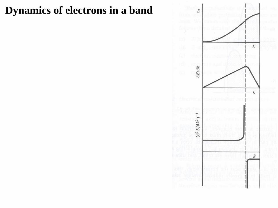
Dynamics of electrons in a band
The external electric field causes a change in the k vectors of all electrons:
Eedt
kdF
If the electrons are in a partially filled band, this
will break the symmetry of electron states in the
1st BZ and produce a net current. But if they are in
a filled band, even though all electrons change k
vectors, the symmetry remains, so J = 0.
E
kx
ap
ap
v
kx
When an electron reaches the 1st BZ edge (at k =
p/a) it immediately reappears at the opposite edge
(k = -p/a) and continues to increase its k value.
As an electron’s k value increases, its velocity
increases, then decreases to zero and then becomes
negative when it re-emerges at k = -p/a!!
E e
dt
k d
Page 51
Dynamics of electrons in a band
Page 52
52
Band-to-band transitions
Page 53
valence
band
conduction
band
Band-to-band transitions
Page 54
gap size
(eV)
InSb 0.18
InAs 0.36
Ge 0.67
Si 1.11
GaAs 1.43
SiC 2.3
diamond 5.5
MgF2 11
valence
band
conduction
band
Band-to-band transitions
Page 55
valence
band
conduction
band
Band-to-band transitions
Page 56
electrons in the conduction band (CB)
missing electrons (holes) in the valence band (VB)
Band-to-band transitions
Page 57
Band-to-band transitions
Page 58
VB maximum
as E=0
conduction band
valence band
free electrons Band-to-band transitions
Page 59
electrons in the conduction band (CB)
missing electrons (holes) in the valence band (VB)
Band-to-band transitions
Page 60
for the conduction band
for the valence band
Both are Boltzmann distributions!
This is called the non-degenerate case.
Band-to-band transitions
Page 61
Band-to-band transitions
Page 62
VBM
CBM
μ
Band-to-band transitions
Page 63
In quantum wells
Band-to-band transitions
Page 64
FYS3410 - Vår 2014 (Kondenserte fasers fysikk) http://www.uio.no/studier/emner/matnat/fys/FYS3410/v14/index.html
Pensum: Solid State Physics by Philip Hofmann (Chapters 1-7 and 11)
Andrej Kuznetsov
delivery address: Department of Physics, PB 1048 Blindern, 0316 OSLO
Tel: +47-22857762,
e-post: [email protected]
visiting address: MiNaLab, Gaustadaleen 23c
Page 65
Lecture schedule (based on P.Hofmann’s Solid State Physics,chapters 1-7 and 11)
Module I – Periodic Structures and Defects 20/1 Introduction. Crystal bonding. Periodicity and lattices, reciprocal space 4h
21/1 Laue condition, Ewald construction, interpretation of a diffraction experimen 2h
22/1 Bragg planes and Brillouin zones (BZ) 2h
23/1 Elastic strain and structural defects 2h
23/1 Atomic diffusion and summary of Module I 2h
Module II - Phonons 03/2 Vibrations, phonons, density of states, and Planck distribution 4h
04/2 Lattice heat capacity: Dulong-Petit, Einstien and Debye models 2h
05/2 Comparison of different models 2h
06/2 Thermal conductivity 2h
07/2 Thermal expansion and summary of Module II 2h
Module III – Electrons 24/2 Free electron gas (FEG) versus Free electron Fermi gas (FEFG) 4h
25/2 Effect of temperature – Fermi- Dirac distribution 2h
26/2 FEFG in 2D and 1D, and DOS in nanostructures 2h
27/2 Origin of the band gap and nearly free electron model 2h
28/2 Number of orbitals in a band and general form of the electronic states 2h
Module IV – Semiconductors 10/3 Energy bands and effective mass method 4h
11/3 Energy bands (continuation) 2h
12/3 Intrinsic semiconductors 2h
13/3 Impurity states in semiconductors and carrier statistics 2h
14/3 p-n junctions and optoelectronic devices 2h
Page 66
Lecture 21: Impurity states in semiconductors and carrier statistics
• Intrinsic and extrinsic semiconductors
• hydrogen-like impurities
• n- and p-type semiconductors
• equilibrium charge carrier concentration
• carriers in non-eqilibrium conditions: diffusion, generation and recombination
Page 67
Lecture 21: Impurity states in semiconductors and carrier statistics
• Intrinsic and extrinsic semiconductors
• hydrogen-like impurities
• n- and p-type semiconductors
• equilibrium charge carrier concentration
• carriers in non-eqilibrium conditions: diffusion, generation and recombination
Page 68
Intrinsic and extrinsic semiconductors
Page 69
iE
pi
ni
Eg
iE
p0
n0
Eg
iE
p0
n0
Eg
Intrinsic and extrinsic semiconductors
Page 70
p0
n0
Eg
Ed
Ei
EID nd
Intrinsic and extrinsic semiconductors
Page 71
Lecture 21: Impurity states in semiconductors and carrier statistics
• Intrinsic and extrinsic semiconductors
• hydrogen-like impurities
• n- and p-type semiconductors
• equilibrium charge carrier concentration
• carriers in non-eqilibrium conditions: diffusion, generation and recombination
Page 72
Hydrogen like impurities in semiconductors
d
Hydrogen-like donor Hydrogen atom
P donor in Si can be modeled as hydrogen-like atom
Page 73
Hydrogen atom - Bohr model
222
0
42
2
0
2
0
22
0
2
2
0
2
2
0
2
22
0
22
0
2
0
2
0
2
2
2
2
0
1
2)4(
2)4( :energy Total
242
1 :energy Kinetic
44 :energy Potential
4
1
4
4)(44
...3,2,1 ,for 4
1
n
emZEK
r
ZeVKE
r
ZemvK
r
Zedr
r
ZeV
n
Ze
mr
nv
mZe
nr
mr
n
mr
nmrrmvZe
nnmvrLr
vm
r
Ze
r
pp
p
pp
p
p
ppp
p
Page 74
Hydrogen atom - Bohr model
eV613)4(2 2
0
40
H .qm
E p
Page 75
eV0.05
2
0s
0
0
*neV613
) π(42
q*n
20s
4
d
Km
m.
K
mE
eV613)4(2 2
0
40
H .qm
E p
Instead of m0, we have to use mn*.
Instead of o, we have to use Ks o.
Ks is the relative dielectric constant
of Si (Ks, Si = 11.8).
Hydrogen-like donor
Hydrogen like impurities in semiconductors
Page 76
p0=0
n0=0
Eg
Ed
Ei
EID
p0
n0
Eg
Ed
Ei
EID nd
Hydrogen like impurities in semiconductors
Page 77
Lecture 21: Impurity states in semiconductors and carrier statistics
• Intrinsic and extrinsic semiconductors
• hydrogen-like impurities
• n- and p-type semiconductors
• equilibrium charge carrier concentration
• carriers in non-eqilibrium conditions: diffusion, generation and recombination
Page 78
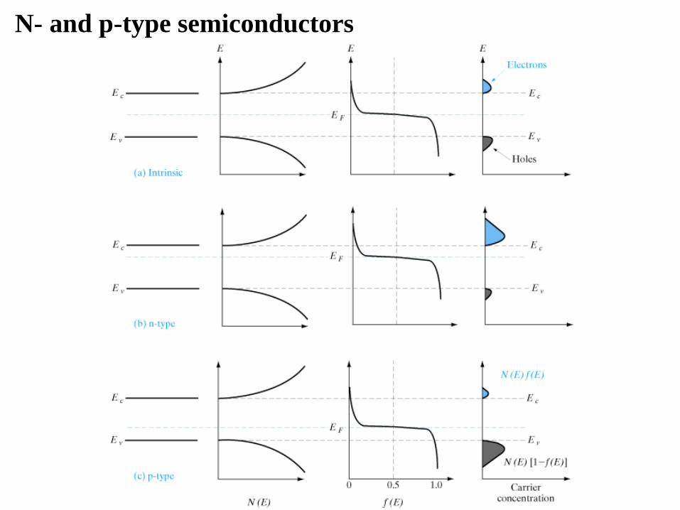
a) Energy level diagrams showing the excitation of an electron from the valence band to the conduction band.
The resultant free electron can freely move under the application of electric field.
b) Equal electron & hole concentrations in an intrinsic semiconductor created by the thermal excitation of
electrons across the band gap
N- and p-type semiconductors
Intrinsic semiconductor
Page 79
a) Donor level in an n-type semiconductor.
b) The ionization of donor impurities creates an increased electron concentration distribution.
N- and p-type semiconductors
n-type Semiconductor
Page 80
a) Acceptor level in an p-type semiconductor.
b) The ionization of acceptor impurities creates an increased hole concentration distribution
N- and p-type semiconductors
p-type Semiconductor
Page 81
N- and p-type semiconductors
Page 82
• Intrinsic material: A perfect material with no impurities.
• Extrinsic material: donor or acceptor type semiconductors.
• Majority carriers: electrons in n-type or holes in p-type.
• Minority carriers: holes in n-type or electrons in p-type.
)2
exp(Tk
Enpn
B
g
i
ly.respective ionsconcentrat intrinsic & hole electron, theare && inpn
e.Temperatur is energy, gap theis TEg
2
inpn
N- and p-type semiconductors
Page 83
donor: impurity atom that increases n
acceptor: impurity atom that increases p
N-type material: contains more electrons than holes
P-type material: contains more holes than electrons
majority carrier: the most abundant carrier
minority carrier: the least abundant carrier
intrinsic semiconductor: n = p = ni
extrinsic semiconductor: doped semiconductor
N- and p-type semiconductors
Page 84
Lecture 21: Impurity states in semiconductors and carrier statistics
• Intrinsic and extrinsic semiconductors
• hydrogen-like impurities
• n- and p-type semiconductors
• equilibrium charge carrier concentration
• carriers in non-eqilibrium conditions: diffusion, generation and recombination
Page 85
Consider conditions for charge neutrality.
The net charge in a small portion of a uniformly doped semiconductor
should be zero. Otherwise, there will be a net flow of charge from one
point to another resulting in current flow (that is against out assumption
of thermal equilibrium).
Charge/cm3 = q p – q n + q ND+ q NA
= 0 or
p – n + ND+ NA
= 0
where ND+ = # of ionized donors/cm3 and NA
= # of ionized acceptors
per cm3. Assuming total ionization of dopants, we can write:
Equilibrium charge carrier concentration in semiconductors
Page 86
Assume a non-degenerately doped semiconductor and assume total ionization of
dopants. Then,
n p = ni2 ; electron concentration hole concentration = ni
2
p n + ND NA = 0; net charge in a given volume is zero.
Solve for n and p in terms of ND and NA
We get:
(ni2 / n) n + ND NA = 0
n2 n (ND NA) ni2 = 0
Solve this quadratic equation for the free electron concentration, n.
From n p = ni2 equation, calculate free hole concentration, p.
Equilibrium charge carrier concentration in semiconductors
Page 87
• Intrinsic semiconductor:
ND= 0 and NA = 0 p = n = ni
• Doped semiconductors where | ND NA | >> ni
n = ND NA ; p = ni2 / n if ND > NA
p = NA ND ; n = ni2 / p if NA > ND
• Compensated semiconductor
n = p = ni when ni >> | ND NA |
When | ND NA | is comparable to ni,, we need to use the charge neutrality
equation to determine n and p.
Equilibrium charge carrier concentration in semiconductors
Page 88
33
17
20
0
2
0 1025.210
1025.2
cmn
np i
kTiEFE
enn i
)(
0
eVn
nkTEE
i
iF 407.0105.1
10ln0259.0ln
10
17
0
Si is doped with 1017 As Atom/cm3. What is the equilibrium
hole concentra-tion p0 at 300°K? Where is EF relative to Ei
Example
Equilibrium charge carrier concentration in semiconductors
Page 89
0 0a dn N p N
Equilibrium charge carrier concentration in semiconductors
Page 90
Lecture 21: Impurity states in semiconductors and carrier statistics
• Intrinsic and extrinsic semiconductors
• hydrogen-like impurities
• n- and p-type semiconductors
• equilibrium charge carrier concentration
• carriers in non-eqilibrium conditions: diffusion, generation and recombination
Page 91
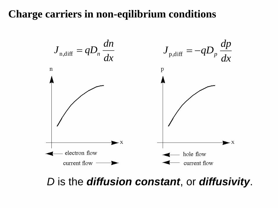
Particles diffuse from regions of higher concentration to regions of lower concentration region, due to random thermal motion.
Charge carriers in non-eqilibrium conditions
Page 92
dx
dnqDJ ndiffn,
dx
dpqDJ pdiffp,
D is the diffusion constant, or diffusivity.
Charge carriers in non-eqilibrium conditions
Page 93
dx
dnqDqnJJJ nndiffndriftnn ε ,,
dx
dpqDqpJJJ ppdiffpdriftpp ε ,,
pn JJJ
Charge carriers in non-eqilibrium conditions
Page 94
• The position of EF relative to the band edges is determined
by the carrier concentrations, which is determined by the
net dopant concentration.
• In equilibrium EF is constant; therefore, the band-edge
energies vary with position in a non-uniformly doped
semiconductor:
Ev(x)
Ec(x)
EF
Charge carriers in non-eqilibrium conditions
Page 95
The ratio of carrier densities at two points depends exponentially on
the potential difference between these points:
1
2i2i112
1
2
i
1
i
2i2i1
i
2Fi2
i
1Fi1
i
1i1F
ln1
lnlnln Therefore
ln Similarly,
ln ln
n
n
q
kTEE
qVV
n
nkT
n
n
n
nkTEE
n
nkTEE
n
nkTEE
n
nkTEE
Charge carriers in non-eqilibrium conditions
Page 96
n-type semiconductor
Decreasing donor concentration
Ec(x)
Ef
Ev(x)
dx
dEe
kT
N
dx
dn ckTEEc Fc /)(
dx
dE
kT
n c
kTEE
cFceNn
/)(
Consider a piece of a non-uniformly doped semiconductor:
Ev(x)
Ec(x)
EF
εqkT
n
Charge carriers in non-eqilibrium conditions
Page 97
If the dopant concentration profile varies gradually with position, then the majority-carrier concentration distribution does not differ much from the dopant concentration distribution.
– n-type material:
– p-type material:
in n-type material
)()()( AD xNxNxn
)()()( DA xNxNxp
)()()()( AD xnxNxpxN
dx
dN
Nq
kT
dx
dn
nq
kT D
D
11
Charge carriers in non-eqilibrium conditions
Page 98
Band-to-Band R-G Center Impact Ionization
Charge carriers in non-eqilibrium conditions
Page 99
Direct R-G Center Auger
Charge carriers in non-eqilibrium conditions
Page 100
Little change in momentum
is required for
recombination
momentum is conserved
by photon emission
Large change in momentum
is required for recombination
momentum is conserved by
phonon + photon emission
Energy (E) vs. momentum (ħk) Diagrams
Direct: Indirect:
Charge carriers in non-eqilibrium conditions
Page 101
0nnn
0ppp
Charge neutrality condition:
pn
equilibrium values
Charge carriers in non-eqilibrium conditions
Page 102
• Often the disturbance from equilibrium is small, such that
the majority-carrier concentration is not affected
significantly:
– For an n-type material:
– For a p-type material:
However, the minority carrier concentration can be
significantly affected.
so |||| 00 nnnpn
so |||| 00 ppppn
Charge carriers in non-eqilibrium conditions
Page 103
n
n
t
n
p
p
t
p
for electrons in p-type material
for holes in n-type material
Consider a semiconductor with no current flow in which
thermal equilibrium is disturbed by the sudden creation
of excess holes and electrons.
Charge carriers in non-eqilibrium conditions
Page 104
Uniformly doped p-type and n-
type semiconductors before the junction is formed. Internal electric-field occurs in
a depletion region of a p-n
junction in thermal equilibrium
Charge carriers in non-eqilibrium conditions