FYS4260/FYS9260: Microsystems and Electronics Packaging and Interconnect Introduction to MEMS technology and processes Micro-electromechanical systems, or MEMS, are micro-scale machines which are manufactured using manufacturing techniques developed for the semiconductor industry. Image credit: Sandia National Labs.
Transcript
FYS4260/FYS9260: Microsystems and Electronics Packaging and Interconnect
Introduction to MEMS technology and processes
Micro-electromechanical systems, or MEMS, are micro-scale machines which are manufactured using manufacturing techniques developed for the
semiconductor industry. Image credit: Sandia National Labs.
– Tummula Fundamentals of Microsystems Packaging, Chapter 14: Fundamentals of Microelectromechanical Systems
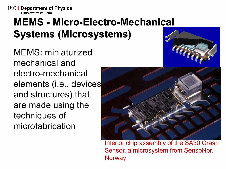
MEMS - Micro-Electro-Mechanical Systems (Microsystems)
MEMS: miniaturized mechanical and electro-mechanical elements (i.e., devices and structures) that are made using the techniques of microfabrication.
Interior chip assembly of the SA30 Crash Sensor, a microsystem from SensoNor, Norway
Introducing the super-hero of this lecture: Silicon • Measured by mass, silicon makes up
27.7% of the Earth's crust and is the second most abundant element in the crust, with only oxygen having a greater abundance
• To properly control the quantum mechanical properties, the purity of the silicon must be very high. Bulk silicon wafers used at the beginning of the integrated circuit making process must first be refined to a purity of 99.9999999% often referred to as "9N" for "9 nines", a process which requires repeated applications of refining technology.
FYS4260/FYS9260 Frode Strisland 4
Monocrystalline silicon ingot grown by the Czochralski processh
"Monokristalines Silizium für die Waferherstellung". Licensed under CC BY-SA 3.0 via Wikimedia Commons - http://commons.wikimedia.org/wiki/File:Monokristalines_Silizium_f%C3%BCr_die_Waferherstellung.jpg#/media/File:Monokristalines_Silizium_f%C3%BCr_die_Waferherstellung.jpg
Silicon is a IV-semiconductor Silicon is located directly beneath carbon Silicon is stable as a crystalline material, but also exist as polycrystalline and amorphous FYS4260/FYS9260 Frode Strisland 5
Silicon in the periodic table
Silicon crystal processing
FYS4260/FYS9260 Frode Strisland 6
"Czochralski Process" by Twisp - Own work,This vector image was created with Inkscape.. Licensed under Public Domain via Wikimedia Commons - http://commons.wikimedia.org/wiki/File:Czochralski_Process.svg#/media/File:Czochralski_Process.svg
Silicon has a face-centered cubic structure (diamond structure) with two atoms associated with each lattice point of the unit cube. One atom is located in position with xyz coordinates (0, 0, 0), the other in position (a/4, a/4, a/4), a being the basic unit cell length.
FYS4260/FYS9260 Frode Strisland 7
"Diamond Cubic-F lattice animation" by original uploader: Brian0918 - http://www.msm.cam.ac.uk/phase-trans/2003/MP1.crystals/MP1.crystals.html ; English Wikipedia. Licensed under CC0 via Wikimedia Commons - http://commons.wikimedia.org/wiki/File:Diamond_Cubic-F_lattice_animation.gif#/media/File:Diamond_Cubic-F_lattice_animation.gif
Diamond cubic crystal structure for silicon
Silicon crystal structure
x yz
3
2
2
1
1
12
Electronic Pack….. Chapter 9 Micro Structure Technology and Micromachined Devices
Slide 8
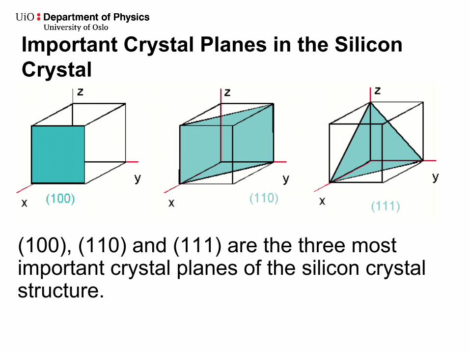
The orientation of of different crystal planes in the basic unit cell can be described by the Miller indices (hkl) between parentheses with each plane defined by a vector description (hx + ky + lz) of the direction perpendicular to that plane. This is related to a coordinate system oriented in parallel with the side edges of the basic cell, with the Miller indices reduced to the smallest possible integers with the same ratio.
Miller Indices for a Plane in a Crystal
Important Crystal Planes in the Silicon Crystal
(100), (110) and (111) are the three most important crystal planes of the silicon crystal structure.
• The (111) plane is the most densely packaged. • No dangling bonds makes this plane most
From http://www.cem.msu.edu/~cem924sg/LowIndexPlanes.html
FYS4260/FYS9260 Frode Strisland 11
Slicing of silicon rods into wires
1. Shaping by grinding
FYS4260/FYS9260 Frode Strisland 12
3. Wafer slicing process using cutting wires (diamond impregnated wires or wires with a grinding slurry)
2. Attachment of silicon rod to wax and wire cut
4. Wafers ready for processing – 4 to 12 inch diameter are standard
Silicon as a Mechanical Material Characteristics
Single Crystal Silicon Stainless Spring Steel
Units
Ultimate Strength
ca. 7,0*109
ca. 2,0*109
N/m2
Yield Strength
ca. 7,0*109
ca. 1,0*109
N/m2
Young's Modulus of Elasticity ca. 1,7*1011
ca. 1,9*1011
N/m2
Shear Modulus
ca. 6,2*1010
ca. 8,2*1010
N/m2
Knoop Hardness
ca. 8,5*109
ca. 6,6*109
N/m2
Density
2,3*103
7,9*103
Kg/m3
Thermal Conductivity 1,6*102
0,33*102
W/m°C
Thermal Expansion
3*10-6
12*10-6
m/m°C
Chemical Resistance Excellent
Fair
Corrosion Resistance Excellent
Fair
Silicon as an Electronic Material Property Value Unit Atomic Number
14
-
Atomic Weight
28,1
-
Atoms per Unit Volume
5 x 10²²
#/cm3
Energy Gap ( 300 °K )
1,1
eV
Intrinsic Resistivity
2,3 x 10⁵ ohm cm
Relative Dielectric Constant
11,7
-
Electron Mobility
1350
cm2/Vsec
Hole Mobility
480
cm2/Vsec
Breakdown Voltage
30
V/µm
In summary - Silicon is a fantastic material! • Structured/crystalline • Mechanically strong • Electrically modifiable through doping • The main work horse of the main bulk of IC and
MEMS devices
FYS4260/FYS9260 Frode Strisland 15
MEMS PROCESSES
FYS4260/FYS9260 Frode Strisland 16
MEMS technology builds on several Batch Processes Adapted from Microelectronics/ IC Technology with no or Minor Modifications: • Photolithography • Spin coating • Etching techniques • Diffusion of dopants • Implantation • Epitaxy • Chemical vapour deposition (CVD) • Thin film technology • Thick film technology
FYS4260/FYS9260 Frode Strisland 17
Batch Processes Mainly Developed for Micromachined Devices
• Bulk micromachining • Surface micromachining • Deep Reactive Ion Etching
Key processes in the clean room • High temperature processes in
furnaces at 400 - 1200 °C
• Deposit various thin layers on the surface
• Etch thin layers
• Making patterns on the wafers
• Etch 3-dimensional structures in the silicon wafer
• Various characterization equipment
• Bond wafers to form a stack
But first – what is a batch process, and why is this important? • The word batch means a group or a pile of something
that can be considered as a unique/consistent within the group
• IC and MEMS batch processing is done on two levels; – Wafer level; produce many devices simultaneously on a
single wafer – Multi-wafer batch processing, e.g. parallell etching of
several wafers at the same time • Driving force for batch processing: $ £ €…
– Faster throughput through expensive machinery – More consistent output
FYS4260/FYS9260 Frode Strisland 20
FYS4260/FYS9260 Frode Strisland 21 21
Short recap: Photolitography
UV-light
Mask
FYS4260/FYS9260 Frode Strisland 22 22
Short intro to micromachining Etching
• RIE (reactive ion etching) • Wet etch
Plasma discharge
Reactive ions (F-, Cl-, O2-,…)
Introduction to microfabrication/microstructuring
• Bulk micromachining: Wet etching based approach taking advantage of the full wafer thickness (subtractive process)
• Surface micromachining: Surface micromachining uses layers deposited on the surface of a substrate as the structural materials, rather than using the substrate itself (additive process)
• High aspect ratio (HAR) silicon micromachining are becoming increasingly important: It combines surface micromachining approaches with deep reactive ion etching forming deep structures in the wafer
FYS4260/FYS9260 Frode Strisland 23
Wet etching • The fundamental reactions are electrochemical in nature. • Holes are injected from the etching solution into the
silicon and Si-atoms are ionized to Si+. • Hydroxyl (OH-) from the etching solution reacts with Si+ to
hydrated silicon. • Hydrated silicon reacts with a complexing agent in the
etching solution to form a soluble reaction product. • The soluble reaction product is dissolved into the etching
solution and carried away from the etching site on the silicon surface into the solution.
• All in all, silicon is etched and the reactant products are diluted into the etching solution.
FYS4260/FYS9260 Frode Strisland 24
A Typical Etching Dewar for Wet Chemical Etching of Silicon
Isotropic* etching • Typical wet isotropic silicon etches are either organic or inorganic
acids such as acetic acid (CH3COOH) or hydrogenfluorid (HF) or mixtures together with water. Often a complexing agent is needed transforming the oxidized product into soluble species.
• By using selective etching techniques in combination with etching time some sort of dimensional control of the etched structure can be obtained. By using spray etching, agitation or light enhanced etching preferred etching directions can be obtained.
• Generally, dimensional accuracy below approximately 30 µm are very hard to achieve, making wet isotropic etching a less favourable and less used method for micromechanics in silicon compared to anisotropic etching.
FYS4260/FYS9260 Frode Strisland 26
*) Isotropic: Similar in all directions
Isotropic etching: Example of etchants and etch rates
FYS4260/FYS9260 Frode Strisland 27
Etchant (Diluent)
Typical Compositions
Temperature [ °C ]
Etch Rate [ µm/ min ]
HF HNO3 CH3COOH + water
10 ml 30 ml 80 ml
22
0,7 - 3,0
HF HNO3 CH3COOH + water
25 ml 50 ml 25 ml
22
40
HF HNO3 CH3COOH + water
9 ml 75 ml 30 ml
22
7,0
A Typical Isotropic Etch Cavity
Isotropic etch cavity in a silicon chip with a square masking film opening. The result is an underetched etch pit with rounded structures.
• An anisotropic etching solution or orientation -dependent etching solution will attack the various crystal directions in single crystal silicon with different speed. Orientation effects during this type of preferential etch have been attributed to crystallographic properties. One explanation is that the atomic bonds in some planes are more exposed than in some others. A suitable designed etching agent will thus attack and strip away certain plane orientations more quickly than others.
• Typical wet anisotropic silicon etches are organic or inorganic alkaline solutions used at elevated temperatures, such as a mixture of ethylene diamine, pyrocatechol and water (EDP-etch) or potassium hydroxide and water (KOH-etch), or tetra-methyl-ammonium-hydroxide (TMAH).. Hydrazine-water mixture are also popular anisotropic silicon etchants.
• These typical anisotropic etching solutions are all characterized by an extremely slow etching speed in the <111> directions of single crystal silicon
Anisotropic Etching of Silicon
Anisotropic Etching of Silicon Etchant (Diluent)
Typical Composition
Temp. [ °C ]
Etch Rate µm/min
Anisotropic Etch Ratio (100)/(111)
Masking Film
Ethylene- diamine Pyrocatechol Water
750 ml 120 gram 100 ml
115
0,75
35:1
SiO2 (2Å/min) Si3N4 (1Å/min) Metals : Au, Cr, Cu, Ta
Ethylene- diamine Pyrocatechol Water
750 ml 120 gram 240 ml
115
1.25
35:1
SiO2 (2Å/min) Si3N4 (1Å/min) Metals : Au, Cr, Cu, Ta
KOH Water & Isopropyl
44 gram 100ml
85
1.4
400:1
SiO2(14Å/min) Si3N4 (1Å/min)
KOH Water & Isopropyl
50 gram 100ml
50
1.0
400:1
SiO2 (14Å/min) Si3N4 (1Å/min)
TMAH Water & Isopropyl
220 gram 780ml
90
1.
100:1
SiO2 (??Å/min)or Si3N4 (0,5 – 2,5 Å/min)
• Lateral etch rate as a function of crystal direction on (110) silicon wafers for an EDP-etch.
• The composition of the etchant was 1l ethylene-diamine, 133 ml water, 160 gram pyrocatechol and 6 gram pyrazine.
• The dashed (111) directions are all equivalent with the (111) direction in single crystal silicon.
Anisotropic Lateral Etch Rate
80 micrometer/hour is around 1.3 micrometer/min
Anisotropic Etch Cavity in (100) Silicon
Anisotropic etch cavity in (100) silicon with a square masking film opening oriented in parallel with the <110> direction. Due to the four-fold symmetry of the slow-etching (111) planes, sideways etching is stopped giving a cavity with four sloped sidewalls. The photography shows such an etched cavity.
Controlling etching depth
1. Estimate and establish etch rates – gives accuracies of ±10-20 micrometer.
2. Chemical selective techniques stopping the etch when an impurity doped chemical resistive layer is reached. Accuracy is typical ±3 micrometer.
3. Electrochemical selective techniques stopping the etch towards a biased p-n junction. This enhances passivation very effectively, giving a typical accuracy of ±1 micrometer.
Surface Micromachining • Surface micromachining can be
defined as a set of methods to make three-dimensional surface structures, with deposition of thin films as additive technique and selective etching of the deposited thin films as subtractive techniques.
• In practice, single crystal silicon wafer is the dominant substrate material, and chemical vapor deposited (CVD) polysilicon is mostly used as the material making up the three-dimensional surface structures.
Surface-micromachined diffraction grating with actuation
Surface Micromachining, continued • A main advantage, compared to bulk micromachining, is that it
does not need double sided processing (back side processing) of the wafers.
• The main additive deposition techniques are evaporation, sputtering, chemical vapor deposition (CVD), and variants of these.
• The main subtractive methods are selective wet etching and dry plasma etching.
• Photolitography is used for pattern definition. • The use of sacrificial layers is important. With this method,
etching of the sacrificial layers underneath non-etched thin film structures can be done. In this way several three-dimensional surface structures can be made, such as cavities, supported microbeams, microstrings, diaphragms, lateral mobile microelements etc.
Surface micromachining example: Cantilever beam
FYS4260/FYS9260 Frode Strisland 36
Surface micromachining is used in making a cantilever: the structural layer is polysilicon, which is released by etching and removing totally the sacrificial layer below, which in this case is silicon oxide. Example from http://81.161.252.57/ipci/courses/technology/inde_374.htm
Surface micromachining example
FYS4260/FYS9260 Frode Strisland 37
Surface micromachining example (2)
FYS4260/FYS9260 Frode Strisland 38
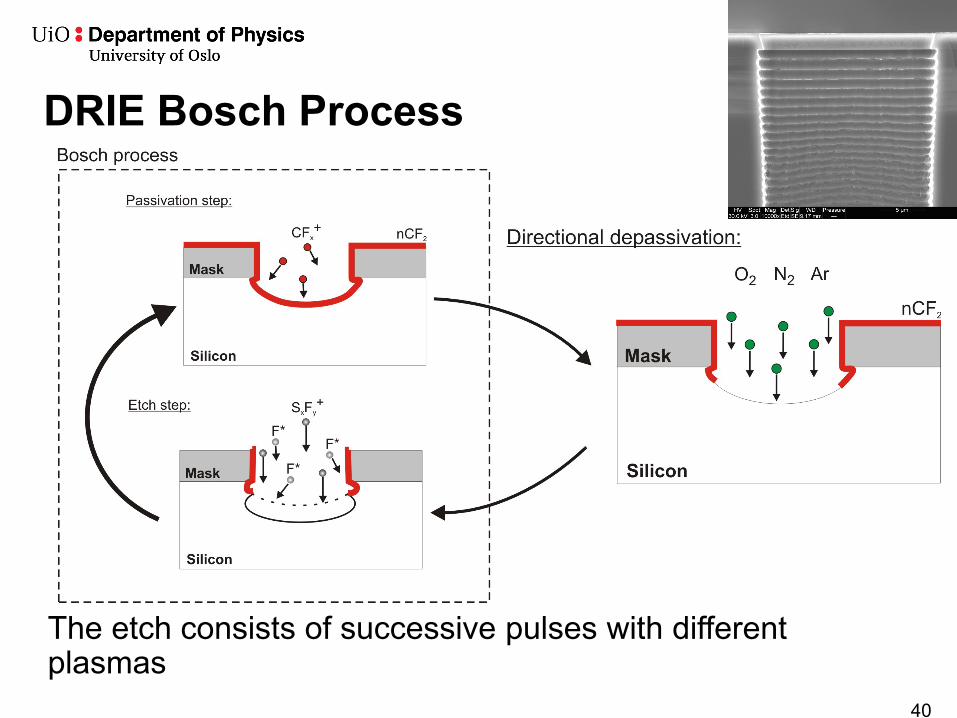
Deep Reactive Ion Etching
• Deep RIE is a highly anisotropic etch process used to create deep penetration, steep-sided holes and trenches in wafers/substrates, typically with high aspect ratios.
• The Bosch-process is the main technique in use
FYS4260/FYS9260 Frode Strisland 39
40
DRIE Bosch Process
The etch consists of successive pulses with different plasmas
DRIE Etching Example: Microfluidic channels for biomedical applications
FYS4260/FYS9260 Frode Strisland 43 43
DRIE example: Vertical electrical feedthrough
• RIE etching from the lower side • POCl3 + oxidation insulation • Poly-Si in hole
1 µm polysilicon
1.2 µm aluminum
FYS4260/FYS9260 Frode Strisland 44
Etched grooves using (a) anisotropic etchants, (b) isotropic etchants, (c) Reactive Ion Etching (RIE) From: http://terpconnect.umd.edu/~sandborn/research/JPL_MEMS/microeng_bulk.html
Summary: Silicon wafer etching techniques
Wafer bonding: Joining wafers
• Anodic Bonding • Direct Wafer Bonding
– Fusion Bonding – Plasma activated bonding
• Metallurgical methods for bonding
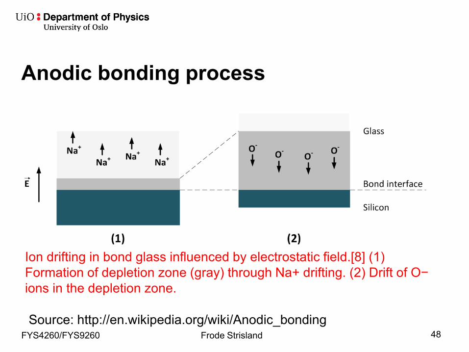
Anodic bonding
Anodic bonding is a wafer bonding process to hermetically seal glass to either silicon or metal without introducing an intermediate layer. This bonding technique is also known as field assisted bonding or electrostatic sealing
FYS4260/FYS9260 Frode Strisland 46
Example of chip made from glass-silicon-glass anodic bonding
Anodic bonding geometry
In anodic bonding, an electrical field is applied to cause ion drift in the (borosilicate) glass which in turn causes bonding
FYS4260/FYS9260 Frode Strisland 47
Scheme of anodic bonding procedure. The top tool works as a cathode and the chunk as anode. The process parameter are bond voltage UB, current limitation IB and bond temperature TB.
Ion drifting in bond glass influenced by electrostatic field.[8] (1) Formation of depletion zone (gray) through Na+ drifting. (2) Drift of O− ions in the depletion zone.
Direct wafer bonding: (Fusion bonding) • Direct bonding describes a wafer bonding
process without any additional intermediate layers. The bonding process is based on chemical bonds between two surfaces.
• Important that joined surfaces have low roughness level (at atomical levels e.g. 3-5 Å) and are planar
FYS4260/FYS9260 Frode Strisland 49
Metallurgical approaches to wafer bonding Soldering/bracing approaches can be used to join wafers. The most common example is the use of deposited gold on wafers, following by an annealing step. The minimum in the liquidus line in the Au-Si phase diagram is at 363 C for 19 at % Si.
FYS4260/FYS9260 Frode Strisland 50
Sensor and actuator principles on a MEMS scale Many fundamental priniciples are applied, including: • Piezoresistivity: Change of resistivity due to a
mechanical force • Capacitive: Change in capacitance due to
changes in mechanical geometry • Piezoelectricity: An applied mechanical force
causes an electrical current • Magnetostriction: Change of resistivity due to a
magnetic field. FYS4260/FYS9260 Frode Strisland 51
52
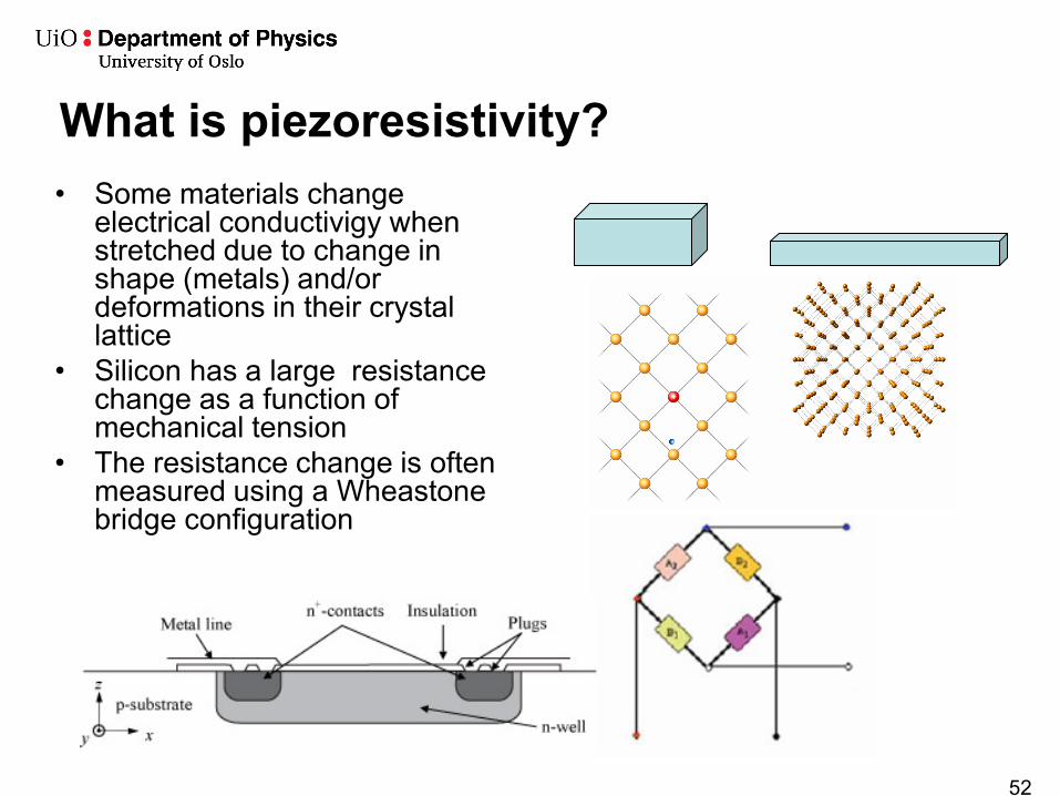
What is piezoresistivity? • Some materials change
electrical conductivigy when stretched due to change in shape (metals) and/or deformations in their crystal lattice
• Silicon has a large resistance change as a function of mechanical tension
• The resistance change is often measured using a Wheastone bridge configuration
Case: MEMS Accelerometer
• Strategy: Measure acceleration from the effect on an inertial mass M.
53
Piezoresistive appraoch
FYS4260/FYS9260 Frode Strisland 54
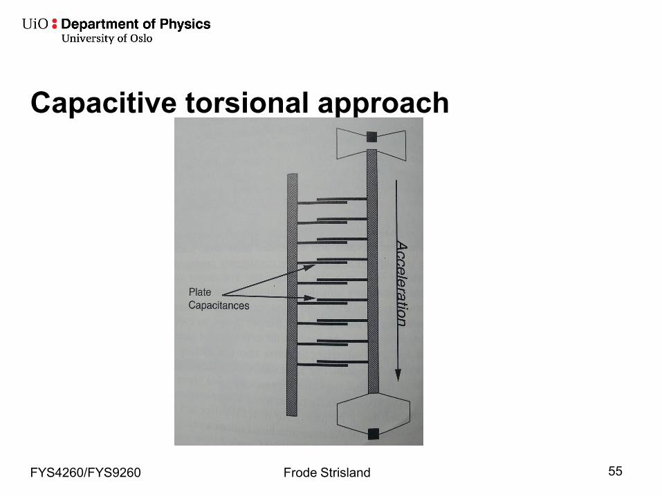
Torsion sensitive axis
Capacitive torsional approach
FYS4260/FYS9260 Frode Strisland 55
Realization of torsional MEMS accelerometer
FYS4260/FYS9260 Frode Strisland 56
Packaging of MEMS: What is the difference from ordinary electronics? • The MEMS package must protect the
micromachined parts in broad ranging environments.
• It must also provide interconnects to electrical signals
• In several cases, provide access to, and interaction withh the external environment.
• We will now exemplify this with a MEMS pressure sensor
FYS4260/FYS9260 Frode Strisland 57
Generic pressure sensor package
FYS4260/FYS9260 Frode Strisland 58
Requirements on a MEMS pressure sensor • The package must ensure that the sensing
device is in intimate contact with the pressurized medium, yet protected from any harmful substances
• Packaging must facilitate access to electrical signals and fluid interconnects.
FYS4260/FYS9260 Frode Strisland 59
Packaging induced stress is a key issue in MEMS • Mechanical sensors will give incorrect
measurements if (thermal) stresses from the package affect the sensitive MEMS components
• Drift in package stresses over time will affect device calibration
FYS4260/FYS9260 Frode Strisland 60
End of lecture: Introduction to MEMS • Important issues:
– You should now have an overview of MEMS processes and sensor principles
– You should also understand why MEMS packaging has additional challenges for the packaging engineer