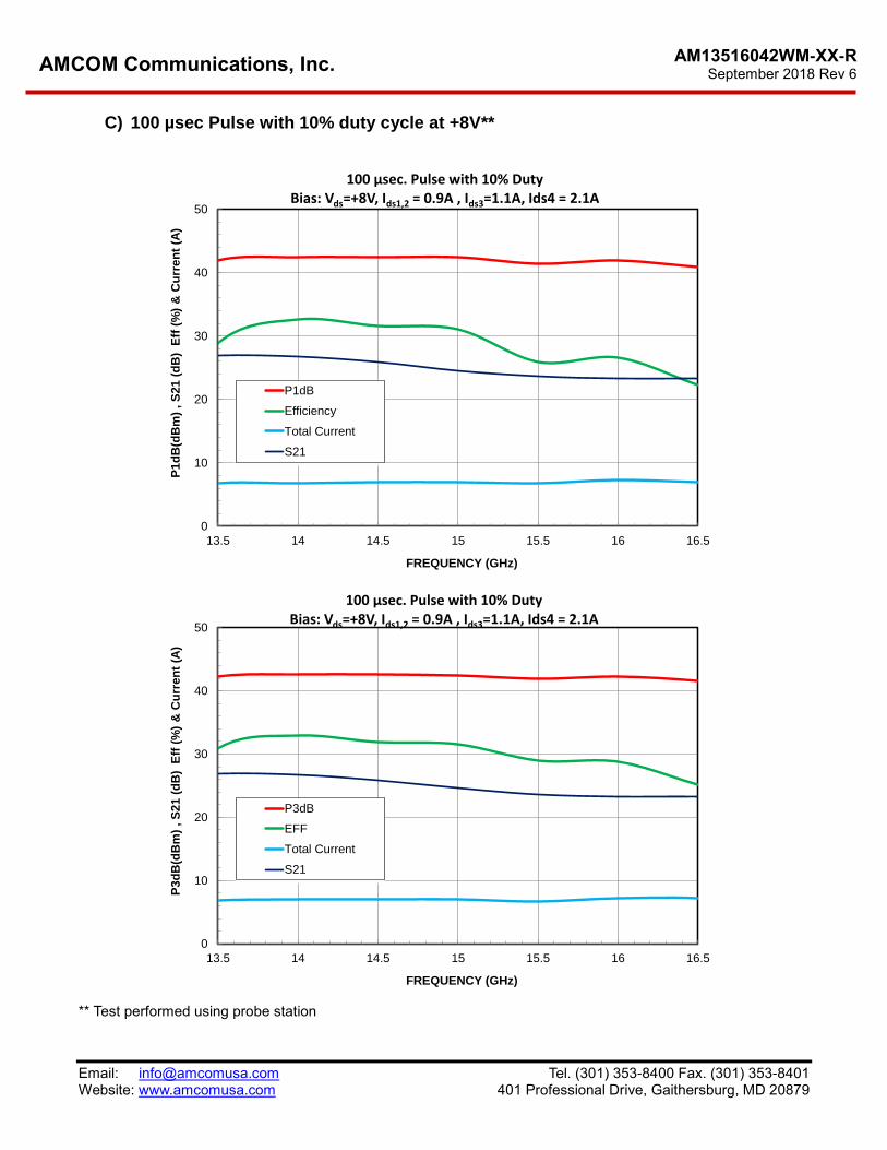
+ All Categories
Home > Documents > GaAs MMIC Power Amplifier - AMCOMUSA · GaAs MMIC Power Amplifier for VSAT & ITU Applications ......

GaAs MMIC Power Amplifier - AMCOMUSA · GaAs MMIC Power Amplifier for VSAT & ITU Applications ......

Date post: 03-Oct-2018
Category:
Upload: lecong
View: 234 times
Download: 0 times
Share this document with a friend
10
Email: [email protected] Tel. (301) 353-8400 Fax. (301) 353-8401 Website: www.amcomusa.com 401 Professional Drive, Gaithersburg, MD 20879 AM13516042WM-XX-R September 2018 Rev 6 GaAs MMIC Power Amplifier for VSAT & ITU Applications DESCRIPTION AMCOM’s AM13516042WM-00-R is a Ku-band GaAs MMIC power amplifier designed for VSAT ground station transmitter applications. It has 23dB small signal gain, and 41dBm (12.6W) P3dB CW output power over the 13.75 to 14.5GHz VSAT band at 8V bias. Under pulsed condition, It has 42dBm (15W) P3dB with 30% PAE. The MMIC PA can also be operated up to 16GHz with over 20dB small signal gain, 40dBm P3dB CW output power and for other ITU band applications such as 14GHz-14.5GHz fixed satellite service (Earth-to-space) for feeder links for the broadcasting satellite service. This frequency band is also applicable to the land mobile satellite service (earth-to-space) on a secondary basis. This product can also be used in 15.4GHz – 15.7GHz for fixed satellite service for connection between earth stations. AM13516042WM-SO-R is the packaged version of the MMIC. TYPICAL PERFORMANCE * (CW bias is Vds = +7V, Idsq1&2 = 1A, Idsq3&4 = 2A ; Bias for 100 µsec. pulse width & 10% duty cycle, is +8V, Idq 1&2 =0.75A, Idq 3&4 =1.5A) Parameters Minimum Typical ** Maximum Frequency Band 1 13.75-14.5GHz Small Signal Gain 23dB Gain Ripple ± 1dB ± 2.0dB P3dB CW / (Pulsed) 10W / (12W) 12W / (15W) Efficiency @ P3dB CW / (Pulsed) 25% / (30%) Frequency Band 2 13.75-16.5GHz Small Signal Gain 22dB Gain Ripple ± 2dB ± 3.0dB P3dB CW / (Pulsed) 7W / (10W) 10W / (15W) Efficiency @ P3dB CW / (Pulsed) 22% / (30%) Input Return Loss 10dB Output Return Loss 5dB Thermal Resistance 1.5°C/W * Specifications subject to change without notice. ** Current may change from lot to lot. Adjust Vgs to reach Idsq1,2=1A, Idsq3,4=2A. *** MMIC could be operated from 5V to 8V without noticeable change in small signal gain performance. APPLICATIONS VSAT ground terminal Fixed satellite service (Earth-to-space) for feeder links Fixed satellite service for connection between earth stations Satellite communications FEATURES Wide bandwidth from 13.5 to 16.0 GHz 42dBm (At 3dB gain compression) of CW output power High gain, 23dB Input /Output matched to 50 Ohms
Transcript

Email: [email protected] Tel. (301) 353-8400 Fax. (301) 353-8401 Website: www.amcomusa.com 401 Professional Drive, Gaithersburg, MD 20879

AM13516042WM-XX-R

September 2018 Rev 6

GaAs MMIC Power Amplifier for VSAT & ITU Applications

DESCRIPTION

AMCOM’s AM13516042WM-00-R is a Ku-band GaAs MMIC power amplifier designed for VSAT ground station

transmitter applications. It has 23dB small signal gain, and 41dBm (12.6W) P3dB CW output power over the 13.75

to 14.5GHz VSAT band at 8V bias. Under pulsed condition, It has 42dBm (15W) P3dB with 30% PAE. The MMIC PA

can also be operated up to 16GHz with over 20dB small signal gain, 40dBm P3dB CW output power and for other

ITU band applications such as 14GHz-14.5GHz fixed satellite service (Earth-to-space) for feeder links for the

broadcasting satellite service. This frequency band is also applicable to the land mobile satellite service

(earth-to-space) on a secondary basis. This product can also be used in 15.4GHz – 15.7GHz for fixed satellite

service for connection between earth stations. AM13516042WM-SO-R is the packaged version of the MMIC.

TYPICAL PERFORMANCE* (CW bias is Vds = +7V, Idsq1&2 = 1A, Idsq3&4 = 2A ; Bias for 100 µsec. pulse width

& 10% duty cycle, is +8V, Idq 1&2 =0.75A, Idq 3&4 =1.5A)

Parameters Minimum Typical ** Maximum

Frequency Band 1 13.75-14.5GHz

Small Signal Gain 23dB

Gain Ripple ± 1dB ± 2.0dB

P3dB CW / (Pulsed) 10W / (12W) 12W / (15W)

Efficiency @ P3dB CW / (Pulsed) 25% / (30%)

Frequency Band 2 13.75-16.5GHz

Small Signal Gain 22dB

Gain Ripple ± 2dB ± 3.0dB

P3dB CW / (Pulsed) 7W / (10W) 10W / (15W)

Efficiency @ P3dB CW / (Pulsed) 22% / (30%)

Input Return Loss 10dB

Output Return Loss 5dB

Thermal Resistance 1.5°C/W

* Specifications subject to change without notice.

** Current may change from lot to lot. Adjust Vgs to reach Idsq1,2=1A, Idsq3,4=2A.

*** MMIC could be operated from 5V to 8V without noticeable change in small signal gain performance.

APPLICATIONS

• VSAT ground terminal

• Fixed satellite service (Earth-to-space) for

feeder links

• Fixed satellite service for connection between

earth stations

• Satellite communications

• 2-way radio

FEATURES

• Wide bandwidth from 13.5 to 16.0 GHz

• 42dBm (At 3dB gain compression) of CW

output power

• High gain, 23dB

• Input /Output matched to 50 Ohms

AMCOM Communications, Inc.

Email: [email protected] Tel. (301) 353-8400 Fax. (301) 353-8401 Website: www.amcomusa.com 401 Professional Drive, Gaithersburg, MD 20879

AM13516042WM-XX-R September 2018 Rev 6

ABSOLUTE MAXIMUM RATING

* De-rate the maximum power dissipation to 40W at 85C

SMALL SIGNAL PARAMETERS

-40

-30

-20

-10

0

10

20

30

40

12 13 14 15 16 17 18

Gain

& R

etu

rn L

osses (

dB

)

Frequency (GHz)

Gain

Input RL

Output RL

Parameters Symbol Rating

Drain source voltage Vds1,2 , Vds3,4 9V

Gate source voltage Vgg -3V

Drain source current Idsq1,2 1.5A

Drain source current Idsq3,4 3A

Continuous dissipation at 25ºC Pt 50W*

Channel temperature Tch 175C

Operating temperature Top -55C to +85C

Storage temperature Tsto -55C to +135C

AMCOM Communications, Inc.

Email: [email protected] Tel. (301) 353-8400 Fax. (301) 353-8401 Website: www.amcomusa.com 401 Professional Drive, Gaithersburg, MD 20879

AM13516042WM-XX-R September 2018 Rev 6

POWER DATA*

A) CW Power at +7V

0

10

20

30

40

50

13.5 14 14.5 15 15.5 16 16.5

Ga

in (

dB

) &

P1

dB

(d

Bm

)

Frequency (GHz)

P1dB (Drain Voltage =+7V, Quiescent Current =3A)

S21

P1dB

Gain (1dB)

EFF

IDS

0

10

20

30

40

50

13.5 14 14.5 15 15.5 16 16.5

Ga

in (

dB

) &

P3

dB

(d

Bm

)

Frequency (GHz)

P3dB (Drain Voltage =+7V, Quiescent Current =3A)

S21

Psat

GAIN (3dB)

EFF

IDS

AMCOM Communications, Inc.

Email: [email protected] Tel. (301) 353-8400 Fax. (301) 353-8401 Website: www.amcomusa.com 401 Professional Drive, Gaithersburg, MD 20879

AM13516042WM-XX-R September 2018 Rev 6

B) CW Power at +6V

* Data corrected for test fixture input and output loss (0.7dB at input and 0.7dB at output)

0

10

20

30

40

50

13.5 14 14.5 15 15.5 16 16.5

Ga

in (

dB

) &

P1

dB

(d

Bm

)

Frequency (GHz)

P1dB (Drain Voltage =+6V, Quiescent Current =3A)

S21

P1dB

Gain (1dB)

EFF

IDS

0

10

20

30

40

50

13.5 14 14.5 15 15.5 16 16.5

Gain

(dB

) &

P3dB

(dB

m)

Frequency (GHz)

P3dB (Drain Voltage =+6V, Quiescent Current =3A)

S21

Psat

GAIN (3dB)

EFF

IDS

AMCOM Communications, Inc.

Email: [email protected] Tel. (301) 353-8400 Fax. (301) 353-8401 Website: www.amcomusa.com 401 Professional Drive, Gaithersburg, MD 20879

AM13516042WM-XX-R September 2018 Rev 6

C) 100 µsec Pulse with 10% duty cycle at +8V**

** Test performed using probe station

0

10

20

30

40

50

13.5 14 14.5 15 15.5 16 16.5

P1d

B(d

Bm

) , S

21 (

dB

) E

ff (

%)

& C

urr

en

t (A

)

FREQUENCY (GHz)

100 µsec. Pulse with 10% DutyBias: Vds=+8V, Ids1,2 = 0.9A , Ids3=1.1A, Ids4 = 2.1A

P1dB

Efficiency

Total Current

S21

0

10

20

30

40

50

13.5 14 14.5 15 15.5 16 16.5

P3

dB

(dB

m)

, S

21

(d

B)

Eff

(%

) &

Cu

rre

nt

(A)

FREQUENCY (GHz)

100 µsec. Pulse with 10% DutyBias: Vds=+8V, Ids1,2 = 0.9A , Ids3=1.1A, Ids4 = 2.1A

P3dB

EFF

Total Current

S21

AMCOM Communications, Inc.

Email: [email protected] Tel. (301) 353-8400 Fax. (301) 353-8401 Website: www.amcomusa.com 401 Professional Drive, Gaithersburg, MD 20879

AM13516042WM-XX-R September 2018 Rev 6

INTERMODULATION DATA

-50

-40

-30

-20

-10

0

0

10

20

30

40

50

0 5 10 15 203rd

IM

D (

dB

c)

Pout (d

Bm

)

Pin (dBm)

C/I3 at 14.0GHz

Pout(dBm)

C/I3

-50

-40

-30

-20

-10

0

0

10

20

30

40

50

0 5 10 15 20

3rd

IM

D (

dB

c)

Pout (d

Bm

)Pin (dBm)

C/I3 at 15.0GHz

Pout(dBm)

C/I3

-50

-40

-30

-20

-10

0

0

10

20

30

40

50

0 5 10 15 20

3rd

IM

D (

dB

c)

Pout (d

Bm

)

Pin (dBm)

C/I3 at 16.0GHz

Pout(dBm)

C/I3

AMCOM Communications, Inc.

Email: [email protected] Tel. (301) 353-8400 Fax. (301) 353-8401 Website: www.amcomusa.com 401 Professional Drive, Gaithersburg, MD 20879

AM13516042WM-XX-R September 2018 Rev 6

CHIP OUTLINE*

* Dimensions in inch

Vgs3Vds3 Vds4Vgs3

Vgs1 Vds1 Vgs2 Vds2 Vds3 Vds4Vgs3

RF in RF out

Vgs1 Vds1 Vgs2 Vds2

AMCOM Communications, Inc.

Email: [email protected] Tel. (301) 353-8400 Fax. (301) 353-8401 Website: www.amcomusa.com 401 Professional Drive, Gaithersburg, MD 20879

AM13516042WM-XX-R September 2018 Rev 6

AM135

16042

SO PACKAGE OUTLINE

Pin Layout

AM135

16042

Pin No. Function Bias

1 Vds1,2 +8V

2 Vgs1,2 -1V

3 RF in NA

4 Vgs1,2 -1V

5 Vds1,2 +8V

6 Vgs3,4 -1V

7 Vds3,4 +8V

8 RF out NA

9 Vds3,4 +8V

10 Vgs3,4 -1V

AMCOM Communications, Inc.

Email: [email protected] Tel. (301) 353-8400 Fax. (301) 353-8401 Website: www.amcomusa.com 401 Professional Drive, Gaithersburg, MD 20879

AM13516042WM-XX-R September 2018 Rev 6

CHIP TEST FIXTURE

Notes:

1. Use epoxy to mount PCB, and eutectic soldering to mount chip.

2. C1=1µF (Dipped Radial Tantalum), C4=100uF (Aluminum Electrolytic) C3=1000pF, C3=20pF R1=50ohms,

R2=10ohms, R3=5ohms.

3. This TF is designed for pulsing the gates, so if pulsing the drains instead, C1 and C4 have to be moved to the

gate DC connectors.

4. All SMT Caps & Resistors are 0402 size (except C1 & C4).

5. Don’t apply Vds1,2,3,4 without proper negative voltages on corresponding gates.

Notes:

1- Use epoxy to mount PCB, and Eutectic soldering to mount chip

2- C1=1uF(Dipped Radial Tantalum),C4=100uF(Aluminum Electrolytic) ,

C2=1000pF, C3=20pF, R1=50ohms, R2=10ohms, R3=5ohms

3- All SMT Caps (except C1 & C4) & Resistors are 0402 size

1 2 3 4 5 6 7 8

16 15 14 13 12 11 10 9

5.2 x 5.1 mm

Chip

10mils 4350

D0007-1963

AMCOM Communications, Inc.

Email: [email protected] Tel. (301) 353-8400 Fax. (301) 353-8401 Website: www.amcomusa.com 401 Professional Drive, Gaithersburg, MD 20879

AM13516042WM-XX-R September 2018 Rev 6

PACKAGE TEST FIXTURE

Notes:

1. Use epoxy to mount PCB.

2. C1=1µF (Dipped Radial Tantalum), C4=100uF (Aluminum Electrolytic) C6=20pF, C7=1000pF, C8=0.47µF,

R1=50ohms, R2=10ohms, R3=5ohms.

3. This TF is designed for pulsing the gates, so if pulsing the drains instead, C1 and C4 have to be moved to the

gate DC connectors.

4. All SMT Caps & Resistors are 0603 size (except C1 & C4). C8 is size 0805.

5. Don’t apply Vds1,2,3,4 without proper negative voltages on corresponding gates.

AM135

16042


Recommended