37
GaAs nanostructures on Si Stefano Sanguinetti LNESS and Dipartimento di Scienza dei Materiali Università di Milano Bicocca, Milano, Italy
| Date post: | 07-Apr-2018 |
| Category: |
Documents |
| Upload: | trinhkhanh |
| View: | 217 times |
| Download: | 1 times |

GaAs nanostructures on SiStefano Sanguinetti
LNESS and Dipartimento di Scienza dei MaterialiUniversità di Milano Bicocca, Milano, Italy
Progress in photonicsOctober 16th
FirenzeOUTLINE
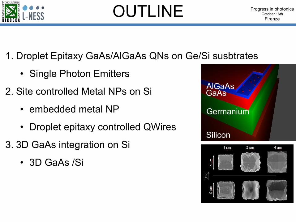
1. Droplet Epitaxy GaAs/AlGaAs QNs on Ge/Si susbtrates
• Single Photon Emitters
2. Site controlled Metal NPs on Si
• embedded metal NP
• Droplet epitaxy controlled QWires
3. 3D GaAs integration on Si
• 3D GaAs /Si
Silicon
Germanium
GaAsAlGaAs
Progress in photonicsOctober 16th
Firenze
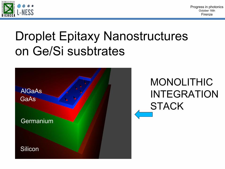
Droplet Epitaxy Nanostructures on Ge/Si susbtrates
Silicon
Germanium
GaAsAlGaAs
MONOLITHIC INTEGRATION STACK
Progress in photonicsOctober 16th
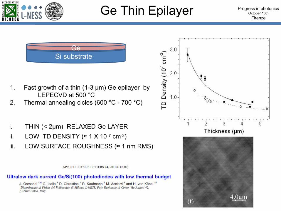
FirenzeGe Thin Epilayer
i. THIN (< 2µm) RELAXED Ge LAYERii. LOW TD DENSITY (≈ 1 X 10 7 cm-2)iii. LOW SURFACE ROUGHNESS (≈ 1 nm RMS)
4.0µm (f)
Ge
1. Fast growth of a thin (1-3 µm) Ge epilayer by LEPECVD at 500 °C
2. Thermal annealing cicles (600 °C - 700 °C)
Si substrate
Progress in photonicsOctober 16th
Firenze
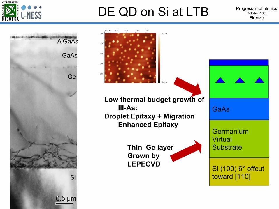
GaAs
Germanium VirtualSubstrate
Si (100) 6° offcut toward [110]
Thin Ge layerGrown by LEPECVD
Low thermal budget growth of III-As:
Droplet Epitaxy + Migration Enhanced Epitaxy
DE QD on Si at LTB
AlGaAs
GaAs
Ge
Si

1.
Al,Ga, In
2.
N, P, As, Sb
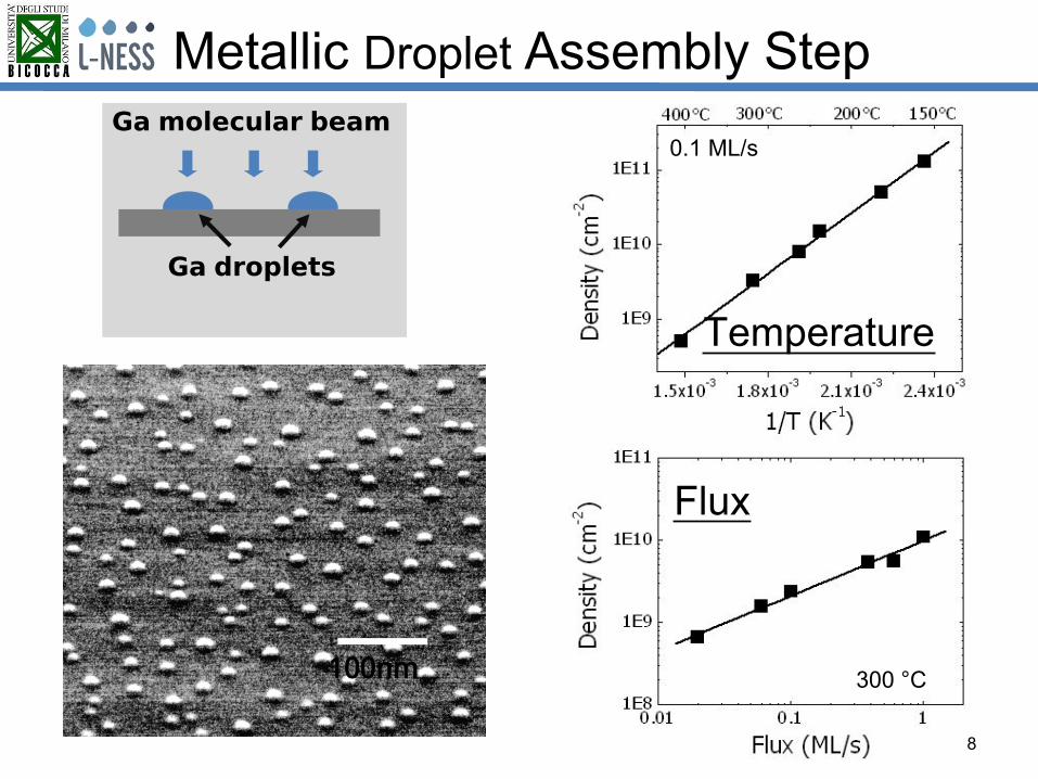
Droplet size, density and distribution control by1.Flux2.Coverage3.Substrate Temperature
Nanostructure morphologycontrol by:1.Flux2.Substrate Temperature
Group III reservoir
deposition (droplets)
III-V crystallization under group V
flux
DE – an MBE two steps process for QN
AdvantagesAdvantages1. Strain independence2. Shape control3. Independent size and density control4. Large Variety of Substrates (including Si)5. Nucleation site position control
6
AlGaA
s
AlGaA
s
GaAs

20 years development
500 nm500 nm
ON Si AND GeON Si AND Ge
MoleculeQUANTUM DOT:QUANTUM DOT:
Circular Exagonal Elongated
Triangular
Arrow
(311) A(311) A (100)(100)(100)(100) (100)(100) (111)A(111)A (111)A(111)A
SingleSingle Multiple ConcentricMultiple ConcentricQUANTUM RING:QUANTUM RING:
Ring-DiskRing-DiskDOT-DiskDOT-Disk
Dot-RingDot-RingDot-DRingDot-DRing
COUPLED NANO-COUPLED NANO-STRUCTURESSTRUCTURES
100nm
Flux
Temperature
0.1 ML/s
300 °C
Ga droplets
Ga molecular beam
8
Metallic Droplet Assembly Step
Progress in photonicsOctober 16th
Firenze
10/25/2015
1.688 1.696 1.704 1.712 1.720
Energy (eV)
10 K
30 K
50 K
70 K
90 K
110 K
130 K
150 KIntensity (arb. units)
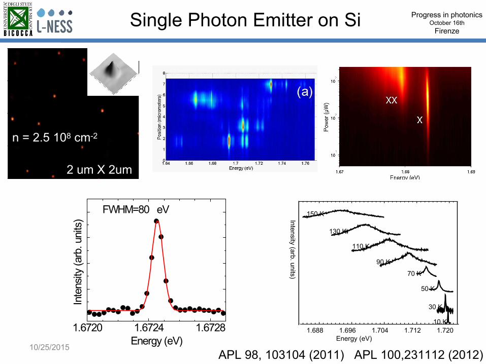
APL 100 (23), 231112 (2012)1.6720 1.6724 1.6728
Inte
nsity
(arb
. uni
ts)
Energy (eV)
FWHM=80 eV
Single Photon Emitter on Si
APL 98, 103104 (2011) APL 100,231112 (2012)
2 um X 2um
n = 2.5 108 cm-2

Progress in photonicsOctober 16th
Firenze
-40 -20 0 20 40
0.25
0.50
0.75
1.00
1.25
1.69 1.70
g(2) ()
Time (ns)
g(2)(0)=0.16
Inte
nsity
(arb
. uni
ts)
Energy (eV)
HBT Measurement at 15 K
-40 -20 0 20 400.0
0.5
1.0
1.5
nT [ns]
gT(2)[0] = 0.17 =0.1
START
STOP
50%BEAMSPLITTER
CORRELATOR
PHOTONSOURCE
DETECTOR 2(STOP)
DETECTOR 1(START)
HISTOGRAM:START-STOPDELAY
Channel
Cou
nts
START
STOP
50%BEAMSPLITTER
CORRELATOR
PHOTONSOURCE
DETECTOR 2(STOP)
DETECTOR 1(START)
HISTOGRAM:START-STOPDELAY
Channel
Cou
nts
DE-QDs on Ge/SiDE-QDs on GaAson Si
on GaAs

Progress in photonicsOctober 16th
Firenze
START
STOP
50%BEAMSPLITTER
CORRELATOR
PHOTONSOURCE
DETECTOR 2(STOP)
DETECTOR 1(START)
HISTOGRAM:START-STOPDELAY
Channel
Cou
nts
START
STOP
50%BEAMSPLITTER
CORRELATOR
PHOTONSOURCE
DETECTOR 2(STOP)
DETECTOR 1(START)
HISTOGRAM:START-STOPDELAY
Channel
Cou
nts
HBT interferometer:second ordercorrelation function
0≤g 2(τ=0 )<1
HBT at 80 K
Progress in photonicsOctober 16th
Firenze
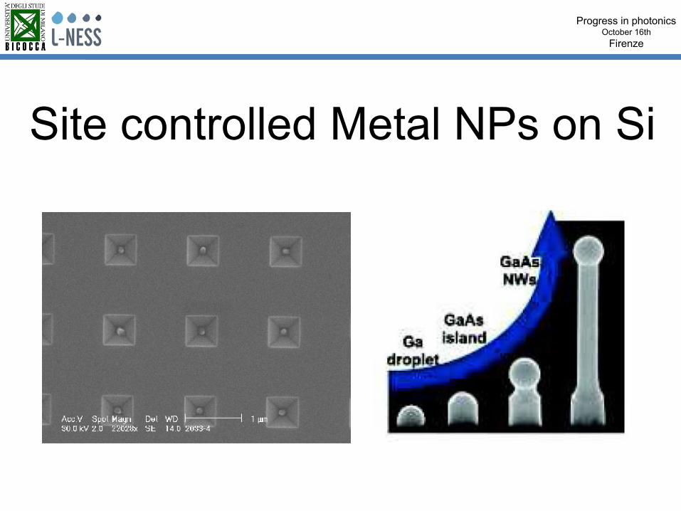
Site controlled Metal NPs on Si

Progress in photonicsOctober 16th
Firenze
ΔG: work of formation of the droplet embryo at constant temperature and pressure
droplet nucleation site control - 1
Surface curvature
Surface tension
Pits, Steps, etc.
Chemical composition, Strain
Droplet Position Control
ΔG modulation over the substrate surface
ΔG = γA + (γint-γsub)Aint – Δμ i

Progress in photonicsOctober 16th
Firenzedroplet nucleation site control
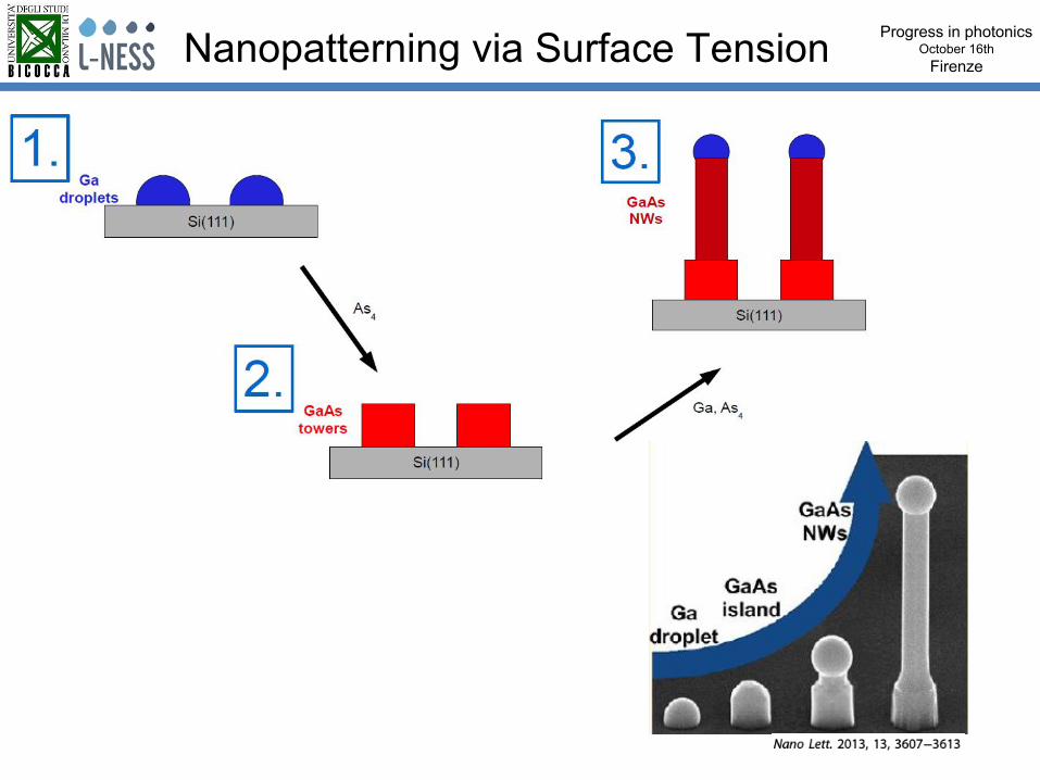
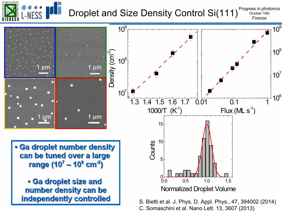
Use of DE to deposit Ga droplets withcontrolled size and density and to grow
GaAs islands on Si (111) surface…
Si
Si
Si
GaAs
ΔG modulation via substrate chemical composition patterning
…and finally to deposit group III atoms whichcreate droplets on top of GaAs only due surface tension modulation introduced on Si by the GaAs nanoislands
SiIn
Si GaAs

Progress in photonicsOctober 16th
Firenzedroplet nucleation site control
On AlGaAs
On Si
ΔG modulation via surface curvature (pits)
M. Bollani et al. Nanotechnology, 25, 205301 (2014)
E. Sala, J. Vac. Sci. Technol. B 32, 061206 (2014)
J. Wu et al. Adv. Funct. Mater., 24, 530 (2014)
Self-assembled
Progress in photonicsOctober 16th
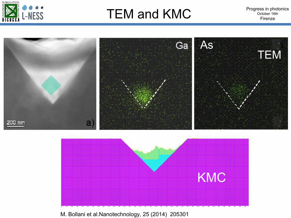
FirenzeTEM and KMC
AsTEM
KMC
M. Bollani et al.Nanotechnology, 25 (2014) 205301

Progress in photonicsOctober 16th
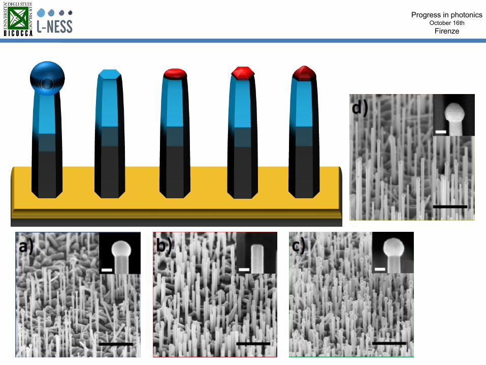
FirenzeTarget 1: NW Density and Size Control
Progress in photonicsOctober 16th
FirenzeNanopatterning via Surface Tension
Progress in photonicsOctober 16th
Firenze
1.3 1.4 1.5 1.6 1.7107
108
109
0.01 0.1 1 106
107
108
109
Dens
ity (c
m-2)
1000/T (K-1)
Flux (ML s-1)
0.0 0.5 1.0 1.50
5
10
15
Coun
ts
Normalized Droplet Volume
Droplet and Size Density Control Si(111)
S. Bietti et al. J. Phys. D. Appl. Phys., 47, 394002 (2014)C. Somaschini et al. Nano Lett. 13, 3607 (2013)

Progress in photonicsOctober 16th
FirenzeDroplet and Size Density Control Si(111)
C. Somaschini et al. Nano Lett. 13, 3607 (2013)

Progress in photonicsOctober 16th
Firenze
C. Somaschini et al. Nano Lett. 13, 3607 (2013)
NW Density (ρ) and Diameter (δ) control
ρ = 4 107/cm2 δ = 120 nm
ρ = 3 108/cm2 δ = 40 nm
On oxidised Si substrates

Progress in photonicsOctober 16th
Firenze
Johanson and Dick, CrystEngComm 13, 7175 K. Dick et al Nano Lett. 12, 3200 (2012)
Sharp interfaces between different semiconductors with different band
structures can form a tunnel barrier for different applications, such as single
electron transistors, resonant tunneling diodes, and memory components.
Target 2: NW sharp Axial Heterostructures
Au Catalyzed MOVPE growth
Self Catalyzed MBE growth
Progress in photonicsOctober 16th
Firenze
10/25/2015
Progress in photonicsOctober 16th
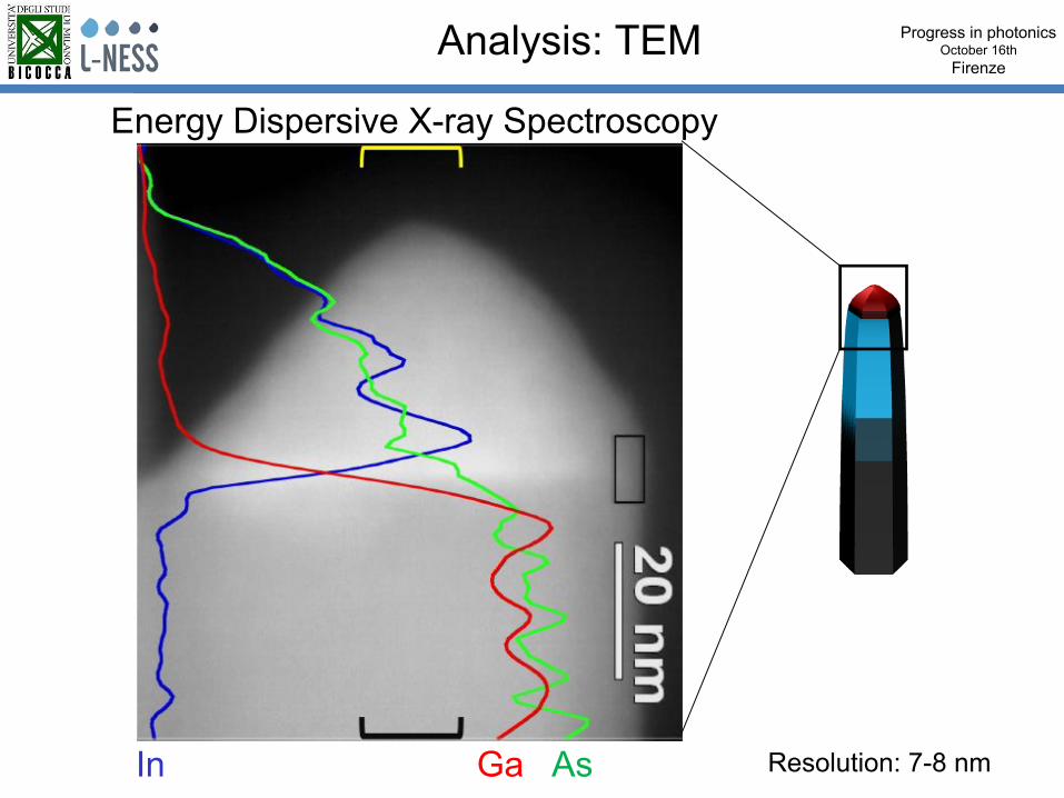
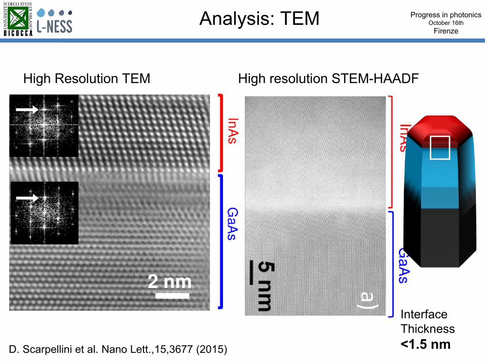
FirenzeAnalysis: TEM
Energy Dispersive X-ray Spectroscopy
In Ga As Resolution: 7-8 nm
Progress in photonicsOctober 16th
Firenze
High resolution STEM-HAADF
Analysis: TEM
InterfaceThickness<1.5 nmD. Scarpellini et al. Nano Lett.,15,3677 (2015)
High Resolution TEM
Progress in photonicsOctober 16th
Firenze
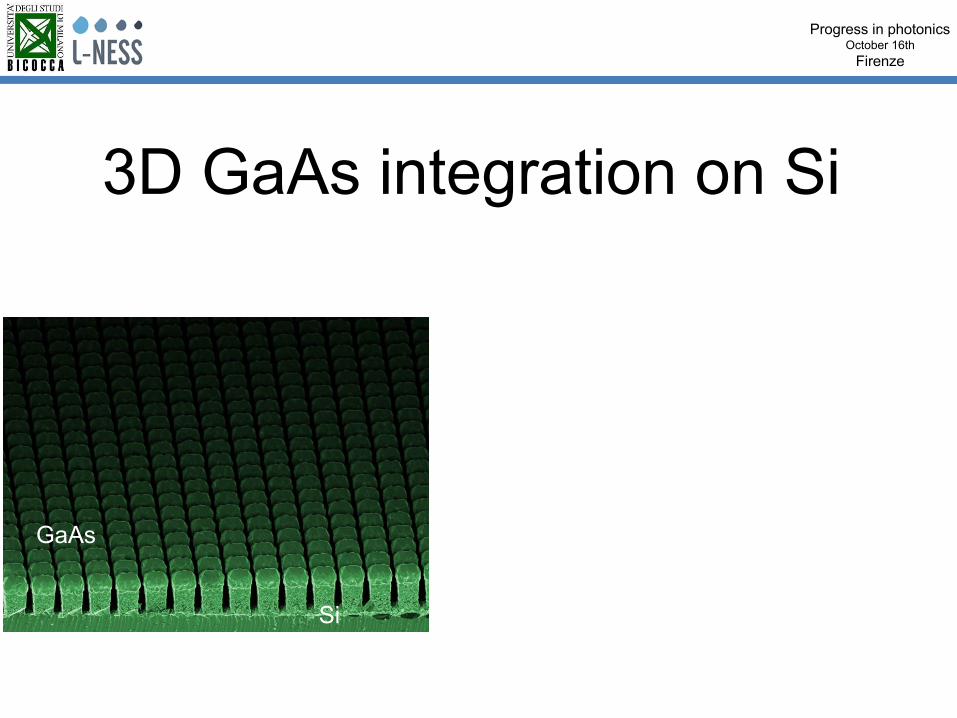
3D GaAs integration on Si
Si
GaAs

Progress in photonicsOctober 16th
Firenze
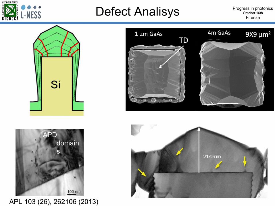
aeas
as
MDsTDs
TDs – threading dislocations MDs – misfit dislocations
<sub
Dislocations, wafer bowing and cracks
Lattice mismatch Thermal mismatchWafer Bowing
Layer Cracking
Integration of mismatched layers
Anti Phase Domains
ae
Stress during cooling/heating

Progress in photonicsOctober 16th
Firenze3D Aspect Ratio Trapping: Ge/Si case
Aspect Ratio Trapping (ART)J. Z. Li et al., APL 91, 021114 (2007)
C. V Falub et al. Science 335 (2012) 1330
PATT
ERN
ED
cracks
UN
PATT
ERN
ED
Ge/Si by LEPECVD
Progress in photonicsOctober 16th
Firenze
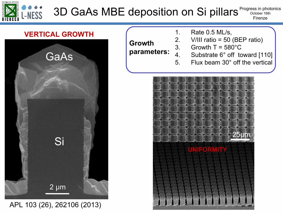
1. Rate 0.5 ML/s, 2. V/III ratio = 50 (BEP ratio) 3. Growth T = 580°C4. Substrate 6° off toward [110] 5. Flux beam 30° off the vertical
2 μm
Si
GaAs
25μm
UNIFORMITY
VERTICAL GROWTH
3D GaAs MBE deposition on Si pillars
Growthparameters:
APL 103 (26), 262106 (2013)
Progress in photonicsOctober 16th
FirenzeDefect Analisys
APD domains
APL 103 (26), 262106 (2013)
Progress in photonicsOctober 16th
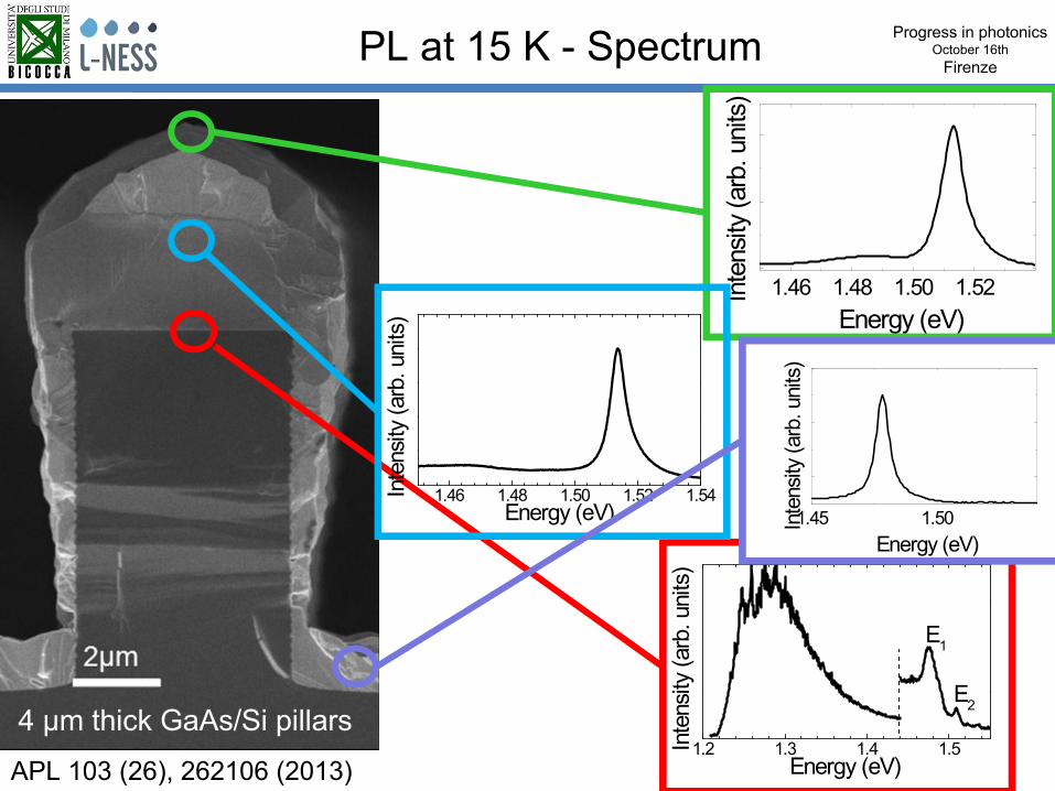
FirenzePL at 15 K - Spectrum
4 µm thick GaAs/Si pillars1.2 1.3 1.4 1.5
E2 I
nten
sity
(arb
. uni
ts)
Energy (eV)
E1
1.46 1.48 1.50 1.52 Inte
nsity
(arb
. uni
ts)
Energy (eV)
1.46 1.48 1.50 1.52 1.54 Int
ensit
y (a
rb. u
nits
)
Energy (eV) 1.45 1.50 Inte
nsity
(arb
. uni
ts)
Energy (eV)
APL 103 (26), 262106 (2013)
Progress in photonicsOctober 16th
Firenze
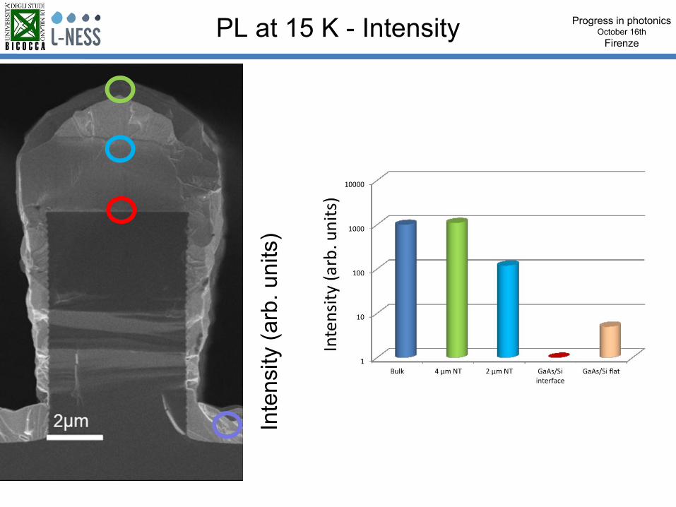
32
PL at 15 K - Intensity
Inte
nsity
(arb
. uni
ts)

Progress in photonicsOctober 16th
Firenze
1.40 1.45 1.50 1.55 1.60
GaAs bulk GaAs/Si pillar
Inte
nsity
(arb
. uni
ts)
Energy (eV)
PL at Room Temperature
334 µm thick GaAs/Si pillars

Progress in photonicsOctober 16th
FirenzeSUMMARY
-40 -20 0 20 40
0.25
0.50
0.75
1.00
1.25
1.69 1.70
g(2) ()
Time (ns)
g(2)(0)=0.16
Inte
nsity
(arb
. uni
ts)
Energy (eV)
Droplet Epitaxy for •integration of GaAs QN based photonic devices on Si• GaAs/Si NW control
3D growth for monolithic integration of GaAs on Si(001)

COLLABORATIONS
Somaschini, ClaudioSalvalaglio, MarcoMarzegalli, AnnaMontalenti, FrancescoBonera, EmilianoMiglio, Leo
Frigeri, CesareGrillo, Vincenzo
CNR-IMEMCNR-S3-Nano
(Italy)
Univ. Milano Bicocca (Italy)
Gurioli, MassimoVinattieri, AnnaBiccari, FrancescoSarti, FrancescoAbbarchi, Marco
Univ. Firenze & LENS (Italy)
Isella, GiovanniFrigerio, JacopoPolitecnico di Milano (Italy)
Geelhar, LutzTrampert, AchimPaul Drude Instituet (Dermany)
University of Michigan (USA) Millunchick, JoannaSmereka, Peter
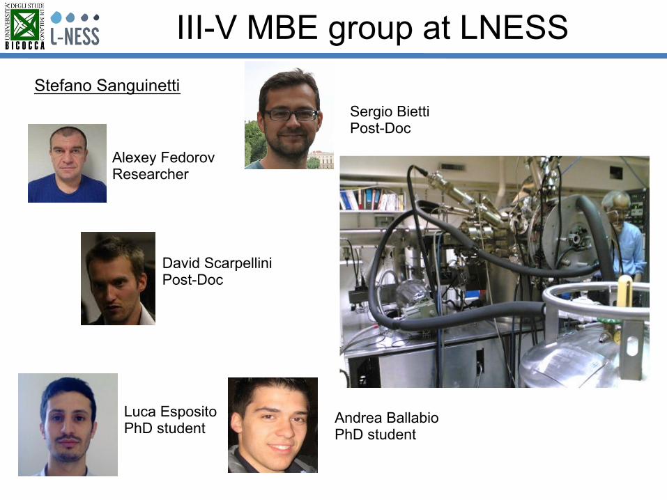
Sergio BiettiPost-Doc
David ScarpelliniPost-Doc
Alexey FedorovResearcher
III-V MBE group at LNESS
Luca EspositoPhD student
Andrea BallabioPhD student
Stefano Sanguinetti

Thank You for Your Attention.
We acknowledge support from:
37


![Optical characterization of type-I to type-II band alignment … · 2017-11-09 · GaAs/AlGaAs material system [2]. To date, many GaAs/ AlGaAs nanostructures, in particular QDs and](https://static.documents.pub/doc/80x56/5e99ea94c8c26a550d1cbb00/optical-characterization-of-type-i-to-type-ii-band-alignment-2017-11-09-gaasalgaas.jpg)


