12 MICROMACHINED INDUCTORS Gabriel M. Rebeiz and Jad Rizk 12.1 INTRODUCTION This chapter summarizes the recent development in micromachined two- dimensional (planar) and three-dimensional inductors. The work di¤ers from the RF MEMS switch and varactors e¤ort because micromachining techniques are used to create high-performance static fixed-value inductors. To date, there has not been a practical implementation of a tunable high-Q inductor (as in the case of RF MEMS varactors), and such inductors are currently synthesized using RF MEMS switches and a set of fixed-value inductors. High-Q inductors are essential for many di¤erent passive and active circuits and can substantially reduce the phase noise or power consumption of oscil- lators and amplifiers. Also, they result in low-loss matching networks and filters (Table 12.1). Micromachined inductors are based on four di¤erent technologies depend- ing on the frequency range: . Thick metal electroplating to reduce the inductor series resistance (this is primarily used at 0.2–6 GHz).* . Three-dimensional solenoid-type inductors to result in large-value designs suitable for 0.2–6 GHz. . Substrate etching underneath the inductor to reduce the parasitic capaci- tance to the substrate (suitable for 1–100 GHz). 359 * One can argue that thick metal electroplating is not part of the micromachining world, but inductors built using this technique have traditionally been included in this field. RF MEMS: Theory, Design, and Technology. Gabriel M. Rebeiz Copyright 2003 John Wiley & Sons, Inc. ISBN: 0-471-20169-3
Transcript
12MICROMACHINED INDUCTORS
Gabriel M. Rebeiz and Jad Rizk
12.1 INTRODUCTION
This chapter summarizes the recent development in micromachined two-dimensional (planar) and three-dimensional inductors. The work di¤ers fromthe RF MEMS switch and varactors e¤ort because micromachining techniquesare used to create high-performance static fixed-value inductors. To date, therehas not been a practical implementation of a tunable high-Q inductor (as in thecase of RF MEMS varactors), and such inductors are currently synthesizedusing RF MEMS switches and a set of fixed-value inductors.
High-Q inductors are essential for many di¤erent passive and active circuitsand can substantially reduce the phase noise or power consumption of oscil-lators and amplifiers. Also, they result in low-loss matching networks and filters(Table 12.1).
Micromachined inductors are based on four di¤erent technologies depend-ing on the frequency range:
. Thick metal electroplating to reduce the inductor series resistance (this isprimarily used at 0.2–6 GHz).*
. Three-dimensional solenoid-type inductors to result in large-value designssuitable for 0.2–6 GHz.
. Substrate etching underneath the inductor to reduce the parasitic capaci-tance to the substrate (suitable for 1–100 GHz).
359
*One can argue that thick metal electroplating is not part of the micromachining world, butinductors built using this technique have traditionally been included in this field.
RF MEMS: Theory, Design, and Technology.Gabriel M. Rebeiz
Copyright 2003 John Wiley & Sons, Inc. ISBN: 0-471-20169-3
. Self-assembly of the inductor away from the substrate to reduce the para-sitic capacitance to the substrate (suitable for 1–100 GHz).
Recently, standard inductor designs on CMOS and SiGe substrates haveresulted in a Q of 12–18 at 2 GHz and 16–22 at 6 GHz. The reasons are many:Modern electromagnetic simulation software allows the user to optimize theinductor geometry for the highest inductance and lowest associated series re-sistance. Also, the substrates used today have a relatively high resistivity (10–2000 W-cm), thereby reducing the eddy current losses underneath the inductor.The inductors are integrated on the top metal layer using a 3-mm-thick goldlayer and are separated from the silicon substrate using 3- to 6-mm-thick oxidelayers. The oxide layers reduce the parasitic capacitance to the substrate, andthey allow the integration of large value inductors without having problemswith the inductor resonant frequency. Micromachined inductors will thereforebe only used for high-Q applications (Q > 30) in low-noise oscillators, high-gain amplifiers, on-chip matching networks, and integrated LC filters. Still,thick-metal electroplating or substrate etching is an additional step in the fab-rication process and results in an increased cost. Currently, there is not a singleCMOS or SiGe RFIC chip on the market which employs a micromachinedinductor of any kind.
12.2 INDUCTOR MODEL AND Q
A general model that describes the performance of a planar inductor (coil) isshown in Fig. 12.1. Ls is the low-frequency inductance, Rs is the series resis-
TABLE 12.1. E¤ect of the Q on Typical Microwave Circuits
Circuit Parameter E¤ect of Q
Oscillator Phase noisea 1=Q 2
Oscillator Power consumptionb 1=QAmplifier Gainc QAmplifier Power consumptiond 1=QMatching network Losse 1=QFilter Lossf 1=QSystem Noise figureg 1=Q
aOscillator phase noise based on an equivalent LC resonator.
bResults in the same phase noise as a standard design, but with reduced power from the source.
cGain is proportional to the load impedance (X ! joL), which is proportional to Q.
dResults in the same gain as a standard design, but with a reduced current (and gm) in thetransistor.
eLoss of matching networks and transmission lines is dependent on the component Q.
fLoss of filters is dependent on the unloaded resonator Q.
gNoise figure is dominated by filter loss, t-line loss, and gain of first-stage amplifier.
360 12 MICROMACHINED INDUCTORS
tance of the coil, Cs is the capacitance between the di¤erent windings of theinductor and includes the fields in air and in the supporting dielectric layers,C1 is the capacitance in the oxide (or polyamide) layer between the coil andthe silicon (or GaAs) substrate, Cp is the capacitance between the coil and theground through the silicon substrate, and Rp is the eddy current losses in thesubstrate. This model has been used extensively by industry and academic labs,and it has been proven to fit very well with Y - and S-parameter measurementsof planar inductors.
12.2.1 Frequency Response of Planar Inductors
The low-frequency value of planar inductors is generally obtained using theGreenhouse formulas [1] or a quasi-static software such as FastHenry [2] or
• •
Figure 12.1. (a) The equivalent LRC model of a planar inductor. (b) A short-circuitedinductor model typically used in S-parameter and Q measurements. Cp1 and Cp2 areoften assumed identical and equal to Cp.
12.2 INDUCTOR MODEL AND Q 361
Agilent ADS [3]. The Greenhouse formulas are not included in this chaptersince they provide only approximate values for the inductance and are easilyfound in the literature. An accurate equivalent model of a planar inductor canbe obtained using a full-wave electromagnetic simulator such as ADS-Mo-mentum [4], Sonnet [5], IE3D [6], or other EM programs. The simulated S-parameters are typically converted to Z or Y parameters and then fitted toobtain accurate values for Ls, Cs, Cp, and Rs. In general, Ls and Rs are fittedusing low-frequency simulations, while Cp and Cs are fitted around the reso-nant frequency of the planar inductor.
At low frequencies, the inductor model of Fig. 12.1 reduces to an Ls;Rs
model, and the input impedance of the inductor is given by
Z ! Rs " joLs #12:1$
However, at high frequencies, the capacitances cannot be neglected, and theinput impedance of the inductor with one side connected to ground is (Fig.12.1b)
Z ! #Rs " joLs$!!!!
1
oCs
" #!!!!1
oC1" 1
oCp1kRp1
" #$ %#12:2$
In general, Rp1 can be neglected and C1 and Cp1 are lumped together in onecapacitance, Cp. A closer look at this model shows a parallel LC resonator witha resistance Rs in series with Ls. Figure 12.2a presents the inductor reactance,X , for Ls ! 5 nH, Rs ! 6:3 W, Cp ! 75 fF, and Cs ! 9 fF. The resistance isdefined at 2 GHz and is assumed to vary as
&&&f
pabove 2 GHz due to the skin
e¤ect (see below). A parallel-type resonance is achieved around 8 GHz, and Xbecomes very large before crashing down to zero and then to negative values.This is confirmed by the phase of Z, which is nearly "90% before resonance andbecomes &90% after resonance (Fig. 12.2b). At resonance ( f ! fr), the inputimpedance of a parallel resonator is real and is given by
Zres !#oLs$2
Rs#12:3$
and Zres ! 5013 W at fr ! 7:95 GHz for the case above. Figure 12.2a showsthat the simple Ls;Rs model, with a constant Ls is valid up to 0:5fr. On theother hand, if one assumes that the inductor is a component which results innearly a "90% phase shift between the voltage and current waveforms, then the
362 12 MICROMACHINED INDUCTORS
planar inductor can be assumed ‘‘inductive’’ up to around 0:85fr even thoughits reactance becomes a strong function of frequency.
12.2.2 Q of Planar Inductors
At low frequencies, and for medium values of Ls resulting in X ! joLs ! 25–70 W, the capacitances can be neglected and the model simplifies to a series
Figure 12.2. The calculated X (a) and phase (b) of a planar 5-nH inductor. The resonantfrequency is 8 GHz and the resistance is assumed constant up to 2 GHz and then in-creases as
&&&f
p.
12.2 INDUCTOR MODEL AND Q 363
Ls;Rs circuit. The inductor Q is defined as
Qconv !energy stored in the inductor
energy lost in a cycle
! 2ojWmj& jWej
Pdiss
! & Im#Y11$Re#Y11$
FjX jRs
! oLs
Rs#12:4$
where Wm and We are the magnetic and electric energy stored in the inductor(in the LsRs circuit, We ! 0) and Y11 is the measured Y parameter of the pla-nar inductor. This definition is not accurate around the resonant frequency ofthe inductor, where jWmj ! jWej, Y11 ! 0, and Qconv ! 0. The resonance oc-curs due to the e¤ect of the parasitic capacitances, and it is unavoidable ininductors unless the capacitance is reduced to zero.
Another definition is
Q ! 2ojWmj" jWej
Pdiss#12:5$
and at resonance, this results in a nonzero Q. However, the authors believe thatthis definition is not based on any physical characteristics and should not beused.
In order to get a better idea of the performance of planar inductors aroundthe resonant frequency, one can numerically insert an ideal capacitor in parallelwith the planar inductor model (Fig. 12.3). By numerically scanning the ca-pacitance of this ideal capacitor, one can obtain a parallel inductor–capacitortank that resonates at di¤erent frequencies. The resonator Q can be determinedusing the standard equation
Q ! o0
2
df
do
''''o!o0
#12:6$
where o0 is the resonant frequency, and f is the phase of the current in theparallel resonator. Since the capacitor is ideal, this results in the inductor Q atdi¤erent frequencies. Figure 12.3 presents the calculated Q of a 5-nH inductorwith a resonant frequency of 10 GHz and Q ! 10 at 2 GHz. As expected, bothmethods result in the same Q at low frequencies, but the resonance method re-sults in a higher Q at 3–8 GHz. At resonance, X ! 0 W, and at f > 8 GHz, theinductor reactance is dominated by the parasitic capacitance and is negative.
364 12 MICROMACHINED INDUCTORS
Still, the resonance method results in a high-Q value since it is a mathematicalsolution.
12.2.3 Measuring Q of Planar Inductors
Planar inductors result in a Q of 10–50 in the 1- to 10-GHz range; therefore, itis quite easy to obtain an accurate Q measurement using S-parameter tech-niques. As shown in Chapter 11, the measured Q is
Q ! 2jIm#S11$j1& jS11j2
#12:7$
Figure 12.3. The calculated Q of a planar 5-nH inductor calculated using the conven-tional method and the resonant-capacitance method. The resonant frequency is 8 GHzand the resistance is assumed constant up to 2 GHz and then increases as
&&&f
p.
12.2 INDUCTOR MODEL AND Q 365
where S11 is the measured reflection coe‰cient of an inductor with one sideshort-circuited (Fig. 12.1). For X ! j50 W (Im#S11$ ! 1), a reflection coe‰-cient of &0:3 dB (jS11j ! 0:966) results in Q ! 30. In this case, an error ofG0.05 dB in the reflection coe‰cient measurement yields a Q of 26–36, whichis quite close to the desired value. Alternatively, the S-parameter measurementscan be transformed to Z or Y parameters and Eq. (12.4) can be used to obtainthe planar inductor Q.
12.2.4 E¤ect of the Metallization Thickness
It was seen in Eq. (12.4) that at low frequencies, and for medium values ofinductance resulting in X ! joLs ! 25–80 W, the limiting factor of Q is the in-ductor series resistance. Accurate electromagnetic analysis based on a fine dis-cretization of the RF current inside the metal conductor have showed that oneneeds a metal thickness of at least 2' skin depth in order to obtain the lowestpossible RF resistance [7, 8]. In this case, the resistance per unit length is givenby
Rs !r
dw#12:8$
where r (W-cm) is the metal resistivity, w is the width of the inductor line, and dis the skin depth given by
d !&&&&&&&&r
pmf
r#12:9$
and m ! 4p' 10&7 H/m is the permeability of free space, and f is the operat-ing frequency. The skin depths for copper ( r ! 1:67 mW-cm), gold ( r !2:35 mW-cm), and aluminum ( r ! 2:65 mW-cm) are shown in Fig. 12.4. Inpractice, the resistivity of plated copper and gold is around 1.3–1.5 times higherthan the bulk values presented above. It is seen that one needs around 5-mm-thick copper and 7-mm-thick gold layers at 1 GHz in order to obtain the RFresistance given by Eq. (12.8). Such metal thickness is typically achieved usingelectroplating techniques. It is important to note that in the case of planar in-ductors, there is an additional resistance that is given by the induced eddy cur-rents within the coil itself [9, 10]. Nowadays, the total inductor resistance canbe accurately modeled using EM software packages [4, 5], and therefore theresistance of Eq. (12.8) should be taken as a starting point.
A reduction in the series resistance greatly increases the Q at low to mediumfrequencies, but has virtually no e¤ect on the reactance or the resonant fre-quency of the planar inductor (Fig. 12.5).
366 12 MICROMACHINED INDUCTORS
12.2.5 E¤ect of the Parasitic Capacitance
The parasitic capacitance in the substrate is the dominant capacitance formedium to large value inductors, and the inductor resonant frequency is givenusing the circuit of Fig. 12.1b
fr F1
2p&&&&&&&&&&&LsCp
p #12:10$
Figure 12.4. Skin depth versus frequency for copper, gold, and aluminum metal layer(bulk values of resistivities are assumed).
Figure 12.5. The e¤ect of the series resistance on the Q of a 5-nH inductor. The resis-tance is assumed constant up to 2 GHz and then increases as
&&&f
p.
12.2 INDUCTOR MODEL AND Q 367
In general, Cs fCp and is neglected in the resonant frequency calculation.However, for micromachined inductors with a very low parasitic capacitanceand a high resonant frequency, one must include Cs in the circuit model. In thiscase, the resonant frequency becomes
fr F1
2p&&&&&&&&&&&&&&&&&&&&&&&&&Ls#Cp " Cs$
p #12:11$
A reduction in the parasitic capacitance not only pushes the resonant fre-quency higher, but also results in a large-reactance, high-Q inductor at highfrequencies. The reason is that the reactance is proportional to f , while theseries resistance is approximately proportional to
&&&&f
p. This is illustrated in Fig.
12.6 for a 5-nH inductor with a Q of around 10 at 2 GHz and a resonant fre-quency of 8 GHz. A reduction in Cp by 80% (from 75 fF to 15 fF) and Cs
by 60% (from 9 fF to 36 fF) increases the resonant frequency to 17 GHz,and it results in a high-Q, high-reactance inductor at 5–13 GHz. However,notice that the Q of the di¤erent inductors is identical at 1–4 GHz becauseit is limited by the low-frequency series resistance.
12.2.6 Goals of Micromachined Inductor Design
There are several goals of micromachined inductors, depending on their circuitapplication and the frequency of operation. For medium inductor valuesj25 < X < j70 W, it is important to reduce the series resistance to result in thehighest possible Q. For large value inductors j70 < X < j250 W or for in-ductors operating at 6–60 GHz, one must reduce the parasitic capacitance soas to push the resonant frequency upwards. Another goal is to result in thesmallest possible chip area for a certain inductance while still maintaining ahigh-Q and a high resonant frequency. This is particularly important for 0.5- to3-GHz applications where the inductor size can be quite large. These inductorssu¤er from a large parasitic and series capacitance, and this can be solved using3-D micromachining techniques (see Section 12.6).
12.3 MICROMACHINING USING THICK METALS LAYERS
The easiest way to result in a high-Q inductor is to use a thick copper processand to isolate the inductor from the silicon substrate using a thick polyamide(or oxide layer). This results in a low C1 and therefore a low Cp, and it pushesthe resonant frequency upwards. The MEMSCAP process employs a thickBCB layer (Benzocyclobutene from Dow Chemical [11]) on top of a siliconsubstrate and uses a 10-mm-thick copper layer (Fig. 12.7). The copper inductoris then passivated using another BCB layer or a PECVD SiO2 layer. The mi-
368 12 MICROMACHINED INDUCTORS
cromachined inductor is post-CMOS compatible and employs low-temperatureprocessing (<100%C).
A Q > 35 was measured for a 1.5-nH square inductor from 3–6 GHz( j28 < X < j56 W), and a 2.1-nH inductor results in Q ! 27–36 at 1–3 GHz( j13 < X < j49 W). The thick copper layer is actually beneficial at high fre-quencies, even if the skin depth is only 1.15 mm at 4 GHz, since the surface area
Figure 12.6. The e¤ect of the substrate capacitance on the Q (a) and X (b) of a 5-nHinductor. The resistance is assumed constant up to 2 GHz and then increases as
&&&f
p.
12.3 MICROMACHINING USING THICK METALS LAYERS 369
for the RF current is increased due to the larger perimeter of the copperinductor (A ! 2#w" t$d, where t is the copper thickness). The MEMSCAPinductor results in a 2'Q improvement over comparable thick metal (3-mmgold) inductors on silicon substrates.
12.4 MICROMACHINING USING SUBSTRATE ETCHING
Substrate etching is primarily done to reduce the e¤ect of the parasitic capaci-tance and to push the resonant frequency of the planar inductor to the highmicrowave region. As mentioned above, this also increases the inductor Q athigh frequencies. However, substrate etching has virtually no e¤ect on the Q
Figure 12.7. The electroplated copper MEMSCAP inductor (a), cross-sectional view (b),and the measured Q of a 1.5-nH inductor [12] (Copyright IEEE).
370 12 MICROMACHINED INDUCTORS
at low frequencies (<2 GHz) since the loss is dominated by Rs and only a thick-metal process will address this issue. Substrate etching is also needed whenbuilding large-value inductors (X > j80 W) since these inductors tend to reso-nate due to the high parasitic capacitances associated with the large multi-turninductor.
The first known work on substrate etching was developed by Chang et al.[13] on CMOS silicon substrates. A planar inductor is suspended on a thin SiO2
membrane using KOH etching and by defining small holes in the SiO2 layer(Fig. 12.8a). The KOH is an anisotropic etch that naturally stops at the h111icrystal planes, and it results in a precise rectangular cavity underneath the in-ductors. The resonant frequency of a 20-turn 125-nH inductor was increasedfrom 800 MHz to 3 GHz using this technique (X ! j628 W at 800 MHz) withan associated Q ! 4. A similar process was done by Sun et al. [14] on a bipolarprocess.
Figure 12.8. Suspended inductors using front-etching techniques and compatible withCMOS processing: UCLA and Delft [13, 14] (a), Carnegie Mellon (b), e¤ort [15](Copyright IEEE).
12.4 MICROMACHINING USING SUBSTRATE ETCHING 371
Lakdawala et al. [15] developed a suspended inductor that is compatiblewith a 0.18-mm CMOS copper interconnect process using RIE techniques (Fig.12.8). The inductor is suspended in a single-anchored (cantilever) or double-anchored configuration over the etched cavity using only the copper and thelow-er dielectric layers (SiO2). The Q of a 3.9-nH inductor improved from 3.9at 2.1 GHz to 17 at 8.6 GHz (X ! j210 W) using this technique. As expected,the Q did not improve at 0.2–2 GHz because the losses are limited by the metalseries resistance. Note that the inductor is completely suspended in air andtherefore is prone to mechanical vibrations. Mechanical simulations indicatethat the motion from an acceleration of 100g is only 0.5 mm due to the smallmass of the inductor (1 mg) and the large spring constant of the thick structureand has virtually no e¤ect on the inductance (only 0.01% change). The firstthree mechanical resonant frequencies are in the range of 8–24 kHz, and thee¤ect of these modes can be compensated by the phased-lock loop (for oscilla-tor design).
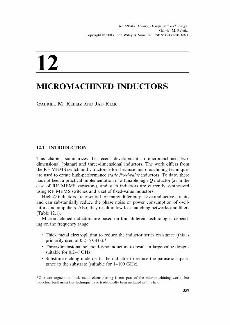
Another membrane process was developed by Chi and Rebeiz [16] on siliconsubstrates using a back-etching method. The inductors are first fabricated onthe top side of the silicon wafer, and an opening is defined on the backside ofthe wafer using infrared alignment. The silicon wafer is then etched using KOHto result in a fully suspended inductor. The resonant frequency of a 1.7-nH in-ductor was pushed from 17 GHz to around 50 GHz using this technique. AQ > 50 is also achieved at 30 GHz for 1.2- to 1.7-nH inductors (X ! j225–320W) and a 1 mm-thick gold layer (d ! 1,700 A at 30 GHz) [16]. Lopez-Villegasused essentially the same process with layout optimization to result in an 8 nHinductor with Q ! 18 at 5 GHz (X ! j250 W), and a 34 nH inductor withQ ! 15–17 at 1–2 GHz (X ! j214–428 W) which is one of the best reportedusing a 2- to 3-mm-thick gold layer (Fig. 12.9) [10].
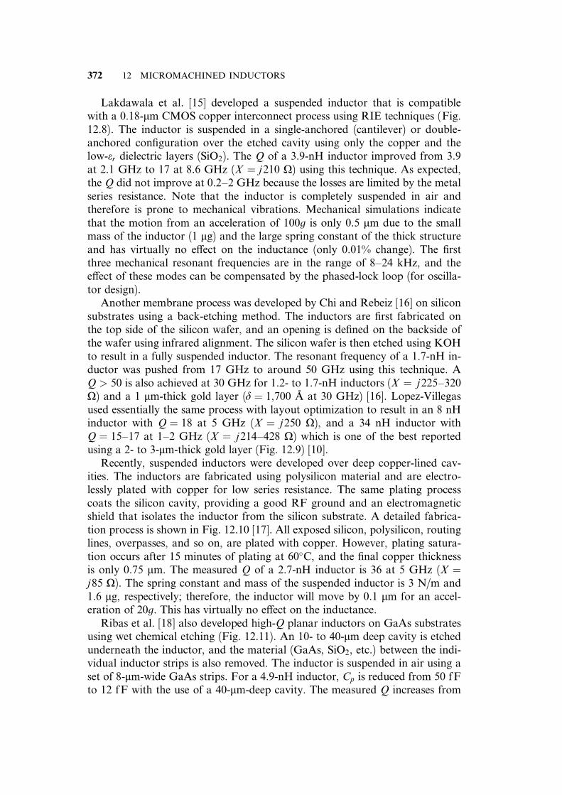
Recently, suspended inductors were developed over deep copper-lined cav-ities. The inductors are fabricated using polysilicon material and are electro-lessly plated with copper for low series resistance. The same plating processcoats the silicon cavity, providing a good RF ground and an electromagneticshield that isolates the inductor from the silicon substrate. A detailed fabrica-tion process is shown in Fig. 12.10 [17]. All exposed silicon, polysilicon, routinglines, overpasses, and so on, are plated with copper. However, plating satura-tion occurs after 15 minutes of plating at 60%C, and the final copper thicknessis only 0.75 mm. The measured Q of a 2.7-nH inductor is 36 at 5 GHz (X !j85 W). The spring constant and mass of the suspended inductor is 3 N/m and1.6 mg, respectively; therefore, the inductor will move by 0.1 mm for an accel-eration of 20g. This has virtually no e¤ect on the inductance.
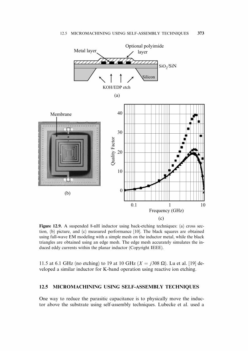
Ribas et al. [18] also developed high-Q planar inductors on GaAs substratesusing wet chemical etching (Fig. 12.11). An 10- to 40-mm deep cavity is etchedunderneath the inductor, and the material (GaAs, SiO2, etc.) between the indi-vidual inductor strips is also removed. The inductor is suspended in air using aset of 8-mm-wide GaAs strips. For a 4.9-nH inductor, Cp is reduced from 50 fFto 12 fF with the use of a 40-mm-deep cavity. The measured Q increases from
372 12 MICROMACHINED INDUCTORS
11.5 at 6.1 GHz (no etching) to 19 at 10 GHz (X ! j308 W). Lu et al. [19] de-veloped a similar inductor for K-band operation using reactive ion etching.
12.5 MICROMACHINING USING SELF-ASSEMBLY TECHNIQUES
One way to reduce the parasitic capacitance is to physically move the induc-tor above the substrate using self-assembly techniques. Lubecke et al. used a
Figure 12.9. A suspended 8-nH inductor using back-etching techniques: (a) cross sec-tion, (b) picture, and (c) measured performance [10]. The black squares are obtainedusing full-wave EM modeling with a simple mesh on the inductor metal, while the blacktriangles are obtained using an edge mesh. The edge mesh accurately simulates the in-duced eddy currents within the planar inductor (Copyright IEEE).
12.5 MICROMACHINING USING SELF-ASSEMBLY TECHNIQUES 373
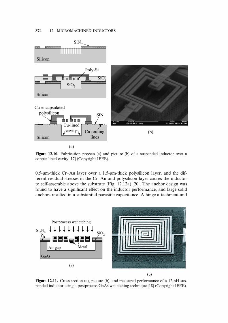
0.5-mm-thick Cr–Au layer over a 1.5-mm-thick polysilicon layer, and the dif-ferent residual stresses in the Cr–Au and polysilicon layer causes the inductorto self-assemble above the substrate (Fig. 12.12a) [20]. The anchor design wasfound to have a significant e¤ect on the inductor performance, and large solidanchors resulted in a substantial parasitic capacitance. A hinge attachment and
Figure 12.10. Fabrication process (a) and picture (b) of a suspended inductor over acopper-lined cavity [17] (Copyright IEEE).
Figure 12.11. Cross section (a), picture (b), and measured performance of a 12-nH sus-pended inductor using a postprocess GaAs wet etching technique [18] (Copyright IEEE).
374 12 MICROMACHINED INDUCTORS
ratchet-locked curling elements have been found to be optimal to assemble theinductor into a semivertical position that changes very little with temperaturevariation (Fig. 12.12b). A 1-nH inductor with a hinge attachment and using athin Cr–Au layer (limited due to the MUMPS fabrication process used [21])resulted in a Q of 13 at 9 GHz (X ! j57 W). The mechanical resonant fre-quency is 500–1500 Hz, depending on the dimensions, and the mechanical Q is20–40. In one case, it took 30g of acceleration to move drive the amplitudeof motion to one-half the original displacement. While this has virtually noe¤ect on the inductance, it does have an e¤ect on the parasitic capacitance and,therefore, on the device X and Q. It is obvious that more work is needed in thisarea to fully characterize these inductors.
Dahlmann et al. [22] developed self-assembly inductors using solder surfacetension. Using a planar process with a photoresist sacrificial layer, copperstructures are fabricated with solder pads placed between an anchored and areleased portion of the devices. When the wafer is heated to 185%C, the solderpads melt, act as hinge drives through the surface tension forces that occur, androtate the structures out of the plane (Fig. 12.13). The wafer is then cooleddown, the solder pads resolidify, and the structure remains assembled in thevertical position. The complete fabrication process is found in reference 23. Themeasured Q at 3 GHz of a 2-nH meander inductor improved from 3 (flat on a1-W-cm silicon substrate) to 15 (90% o¤ the substrate).
It is important to note that while self-assembled inductors couple virtuallyzero energy into the substrate, they do couple to each other using electromag-netic radiation. This can cause EM interference in a transceiver system. There-fore, careful EM simulation must be done before these inductors are used inpractical systems.
Figure 12.12. Picture (a) and measured Q (b) of a self-assembled 1.2-nH inductor [20](Copyright IEEE).
12.5 MICROMACHINING USING SELF-ASSEMBLY TECHNIQUES 375
12.6 ELEVATED AND SOLENOID-TYPE COPPER INDUCTORS
Solenoid-type inductors result in a confined magnetic field inside of the sole-noid, and they do not couple much to the silicon substrate if suspended highabove the substrate. Yoon et al. [24, 25] developed solenoid inductors on siliconand glass substrates using a multiple exposure and single development methodon a thick photoresist mold (Fig. 12.14). The top part of the solenoid is thenfabricated using a single-step copper electroplating process. The photoresistmold is 45- to 60-mm-deep and is capped by a 20- to 30-mm-thick copper layer.The cross-sectional area of the solenoid is around 60' 60 mm2.
Yoon et al. [24, 25] found that the standard formula of solenoid inductancegiven in EM textbooks did not agree well with the measured values of Ls. Thereason is that the cross-sectional area of the solenoid is quite small and themagnetic field is not well-confined inside the solenoid. In one process, the sole-noid was separated from the silicon substrate (10- to 20-W-cm) using a 15-mm-thick polyamide layer and resulted in Q ! 17 at 2.4 GHz for a 2.7-nH inductor.This is due to the fringing magnetic fields inside the silicon substrate that in-duces eddy currents and therefore loss, since the solenoid area cannot con-tain all of the magnetic field. When the solenoid is placed on a glass substrate(Corning 7740), the measured Q of a 2.6-nH inductor increased to >20 at4–7 GHz (Q ! 24 at 5.5 GHz, X ! j83 W).
Chen et al. developed a solenoid-type inductor using a photoresistive epoxy(SU-8) mold and thick copper electroplating (Fig. 12.15) [26, 27]. The SU-8 isnot removed and the inductor is embedded in this epoxy, which exhibits lowloss at microwave frequencies after a hard bake process (to remove any watertrapped in the photoresist). The 6-turn inductor is also built on top of a 50-mm-
Figure 12.13. (a) Out-of-plane meander-type inductors after self-assembly, and (b) ablow-up of the solder hinges after heating [22, 23] (Copyright IEEE).
376 12 MICROMACHINED INDUCTORS
Figure 12.14. Fabrication process (a), picture (b), and measured performance (c) of a2.4-nH all-copper solenoid inductor on silicon and glass substrates [24, 25] (CopyrightIEEE).
12.6 ELEVATED AND SOLENOID-TYPE COPPER INDUCTORS 377
thick SU-8 layer to isolate it from the CMOS substrate, and it has a cross-sec-tional area of 20' 20 mm2. A measured Q of 21 was achieved for a 2.6-nHinductor at 2.4 GHz (X ! j82 W), which is competitive with other micro-machined designs.
The solenoid-type inductor was taken to extremes using a large aluminacore placed manually on a silicon substrate (Fig. 12.16) [28]. In this case, thecross-sectional area is equal to the core dimensions and is 650' 500 mm2. Also,the magnetic field center is around 300 mm above the substrate. An electro-plated photoresist is deposited on the alumina core and exposed using a three-dimensional maskless direct-write laser lithography tool. After developing theexposed resist, 5- to 10-mm copper metal layers are electroplated on the threesides of the alumina core, followed by a Ni/Au electrolytic deposition for pas-sivation. One-turn (4.9-nH) and four-turn (14-nH) inductors resulted in Q ! 30and Q ! 17 at 1 GHz and 0.7 GHz, respectively. While this method hasachieved the highest Q to date at 1 GHz, it is not practical for low-cost im-plementations due to the manual placement of the alumina core over the siliconsubstrate.
Figure 12.15. Fabrication process of the SU-8 micromachined inductor [26] (CopyrightIEEE).
Figure 12.16. A solenoid-type four-turn inductor using a large alumina core [28] (Copy-right IEEE).
378 12 MICROMACHINED INDUCTORS
Figure 12.17. Fabrication process (a), picture (b), and measured performance (c) of anoverhang inductor using 15-mm-thick copper layers [29, 30] (Copyright IEEE).
12.6 ELEVATED AND SOLENOID-TYPE COPPER INDUCTORS 379
A more interesting approach is to suspend a thick-metal planar inductorabove the silicon substrate using an air gap (Fig. 12.17) [29–31]. This technol-ogy addresses well the inductor limitations and results in a low parasitic ca-pacitance and a low series resistance (copper electroplating). Electromagneticanalysis indicates that substrate coupling can be eliminated if the inductor isplaced at least 30 mm from the substrate. This has been done using the sacrifi-cial metallic mold (SMM) process and 10- to 15-mm-thick copper layers (Fig.12.17c). The SMM can be fabricated on silicon or glass substrates, and manylayers can be added to create transformers or multilevel inductors. A 14-nHinductor having Q ! 38 at 1.8 GHz (X ! j158 W) was developed with an areaof less than 500 mm2 [30, 31]. Also, 4.8-nH and 1.75-nH inductors resulted inQ ! 35 and 57 at 5 GHz (X ! j151 W) and 10 GHz (X ! j110 W), respec-tively. In our opinion, this is the best work on planar inductors to-date.
12.7 CONCLUSION
This chapter summarized the recent development in micromachined high-Qinductors for RF and microwave applications. The substrate etching techniqueis useful for high-frequency applications or for large-value inductors, and thethick copper electroplating technique is ideal for low-frequency applications(0.2–5 GHz). Of particular importance is the recent work of Yoon et al. [29–31] on elevated copper inductors which results in small size inductors and out-standing Q from 1 GHz to 10 GHz. The main limitations to high-Q inductorsis their increased fabrication cost and special handling in the case of substrateetching. However, the authors predict that they will eventually be integratedwith CMOS and SiGe transistors for low phase-noise oscillators and high-e‰ciency power amplifiers. Also, high-Q inductors are ideal for tunable LCfilters in multiband communication systems.
Bibliography
[1] H. M. Greenhouse, Design of planar rectangular microelectronic inductors, IEEETrans. Parts, Hybrids, Packag., Vol. PHP-10, pp. 101–109, June 1974.
[2] B. Guan, P. Rott, and M. J. Feldman, Fasthenry 2.0R, University of Rochester,Rochester, NY.
[3] Agilent Technologies, Advanced Design System, Palo Alto, CA, www.agilent.com.
[7] T. E. VanDeventer, L. P. B. Katehi, and A. C. Cangellaris, An integral equationmethod for the evaluation of conductor and dielectric losses in high-frequencyinterconnects, IEEE Trans. Microwave Theory Techn., Vol. 37, No. 12, pp. 1964–1972, December 1989.
380 12 MICROMACHINED INDUCTORS
[8] W. Heinrich, Full-wave analysis of conductor losses on MMIC transmission lines,IEEE Trans. Microwave Theory Tech., Vol. 38, pp. 1468–1472, October 1990.
[9] W. B. Kuhn and N. M. Ibrahim, Analysis of current crowding e¤ects in multiturnspiral inductors, IEEE Trans. Microwave Theory Tech., Vol. 49, No. 1, pp. 31–38,January 2001.
[10] J. M. Lopez-Villegas, J. Samitier, C. Cane, P. Losantos, and J. Bausells, Improve-ment of the quality factor of RF integrated inductors by layout optimization, IEEETrans. Microwave Theory Tech., Vol. 48, No. 1, pp. 76–83, January 2000.
[11] The Dow Chemical Company, www.dow.com, www.dow.com/cyclotene.
[12] MEMSCAP Inc., San Jose, CA, www.memscap.com. Also presented at many IEEEMTT-S Workshops.
[13] J. Y.-C. Chang, A. A. Abidi, and M. Gaitan, Large suspended inductors and theiruse in a 2 mm CMOS RF amplifier, IEEE Electron Device Lett., Vol. 14, pp. 246–248, May 1993.
[14] Y. Sun, J. L. Tauritz, and R. G. F. Baets, Micromachined RF passive componentsand their applications in MMICs, Int. J. RF Microwave CAE, Vol. 9, pp. 310–325,1999.
[15] H. Lakdawala, X. Zhu, S. Santhanam, L. R. Carley, and G. K. Fedder, Micro-machined high-Q inductors in a 0.18 mm copper interconnect low-k dielectricCMOS process, IEEE J. Solid-State Circuits, Vol. 37, No. 3, pp. 394–403, March2002.
[16] C.-Y. Chi and G. M. Rebeiz, Planar microwave and millimeter-wave lumpedelements and coupled-line filters using micro-machining techniques, IEEE Trans.Microwave Theory Tech., Vol. 43, No. 4, pp. 730–738, April 1995.
[17] H. Jiang, Y. Wang, J.-L. A. Yeh, and N. C. Tien, On-chip spiral inductors sus-pended over deep copper-lined cavities, IEEE Trans. Microwave Theory Tech., Vol.48, No. 12, pp. 2415–2423, December 2000.
[18] R. P. Ribbas, J. Lescot, J. L. Leclerq, J. M. Karam, and F. Ndagijimana, Micro-machined microwave planar spiral inductors and transformers, IEEE Trans.Microwave Theory Tech., Vol. 48, No. 8, pp. 1326–1335, August 2000.
[19] L.-H. Lu, P. Bhattacharya, L. P. B. Katehi, and G. E. Ponchak, X-band andk-band lumped wilkinson power dividers with micromachined technology, in IEEEMTT-S International Microwave Symposium Digest, June 2001, pp. 287–290.
[20] V. M. Lubecke, B. Barber, E. Chan, D. Lopez, M. E. Gross, and P. Gammel, Self-assembly MEMS variable and fixed RF inductors, IEEE Trans. Microwave TheoryTech., Vol. 49, No. 11, pp. 2093–2098, November 2001.
[21] D. A. Koester, R. Mahadevan, and K. W. Markus, MUMPs Introduction and De-sign Rules, MCNC MEMS Technology Applications Center, 1994.
[22] G. W. Dahlmann, E. M. Yeatman, P. R. Young, I. D. Robertson, and S.Lucyszyn, MEMS high Q microwave inductors using solder surface tension self-assembly, in IEEE MTT-S International Microwave Symposium Digest, June 2001,pp. 394–403.
[23] P. W. Green, R. R. A. Syms, and E. M. Yeatman, Self assembly of three-dimensional microstructures using rotation by suface tension forces, IEEE J.Microelectromech. Syst., Vol. 4, No. 4, pp. 170–, December 1995.
[24] J.-B. Yoon, B.-K. Kim, C.-H. Han, E. Yoon, K. Lee, and C.-K. Kim, High-
BIBLIOGRAPHY 381
performance electroplated solenoid-type integrated inductor (SI2) for RF applica-tions using simple 3D surface micromachining technology, in IEEE InternationalElectron Device Meeting, December 1998, pp. 544–547.
[25] J.-B. Yoon, B.-K. Kim, C.-H. Han, E. Yoon, and C.-K. Kim, Surface micro-machined solenoid on-Si and on-glass inductors for RF applications, IEEE Elec-tron Device Lett., Vol. 20, pp. 487–489, September 1999.
[26] Y. E. Chen, Y. K. Yoon, J. Laskar, and M. Allen, A 2.4 GHz integrated CMOSpower amplifier with micromachined inductors, in IEEE MTT-S International Mi-crowave Symposium Digest, June 2001, pp. 67–70.
[27] J. M. Shaw, J. D. Gelorme, N. C. LaBianca, W. E. Conley, and S. J. Holmes,Negative photoresists for optical lithography, IBM J. Res. Dev., Vol. 41, pp. 81–94, 1997.
[28] D. J. Young, V. Malba, J.-J. Ou, A. F. Bernhardt, and B. E. Boser, Monolithichigh-performance three-dimensional coil inductors for wireless communication ap-plications, in IEEE International Electron Device Meeting, December 1997, pp. 67–70.
[29] J.-B. Yoon, C.-H. Han, E. Yoon, and C.-K. Kim, Monolithic integration of 3-Delectroplated microstructures with unlimited number of levels using planarizationwith a sacrificial metallic mold (PSMM), in IEEE International Conference onMicroelectromechanical Systems, January 1999, pp. 624–629.
[30] J.-B. Yoon, C.-H. Han, E. Yoon, and C.-K. Kim, High-performance three-dimensional on-chip inductors fabricated by novel micromachining techbology forRF MMIC, in IEEE MTT-S International Microwave Symposium Digest, June1999, pp. 1523–1526.
[31] J.-B. Yoon, C.-H. Han, E. Yoon, and C.-K. Kim, Monolithic high-Q overhanginductors fabricated on silicon and glass substrates, in IEEE International ElectronDevice Meeting, December 1999, pp. 753–756.