88
GaN Transistors for Efficient Power Conversion

GaN Transistors for Efficient Power Conversion

Agenda
• How GaN works • Electrical Characteristics • Design Basics • Design Examples • Summary
2 2

How GaN Works
3 3

The Ideal Power Switch • Block Infinite Voltage • Carry Infinite Current • Switch In Zero Time • Zero Drive Power • Normally Off
4 4
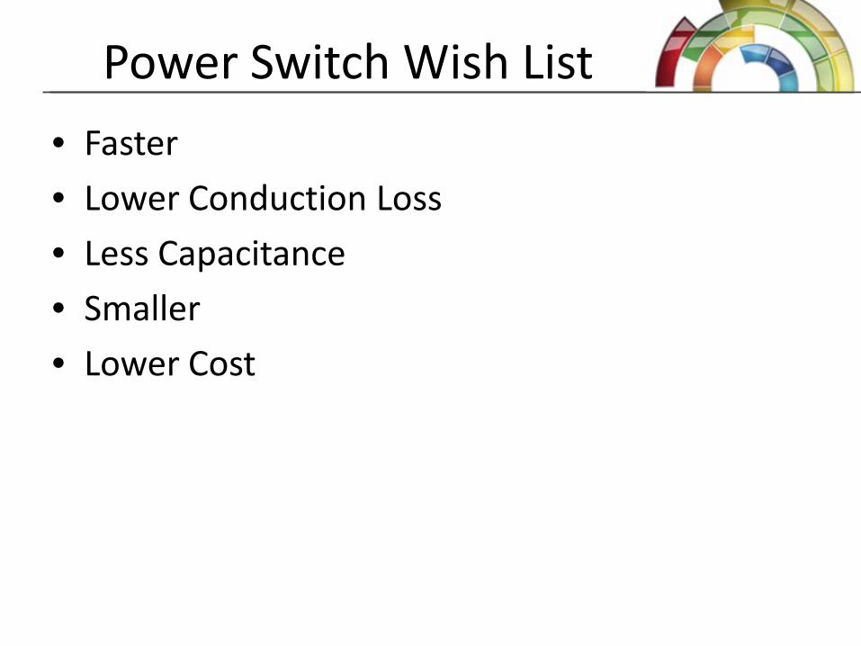
Power Switch Wish List • Faster • Lower Conduction Loss • Less Capacitance • Smaller • Lower Cost
5
6
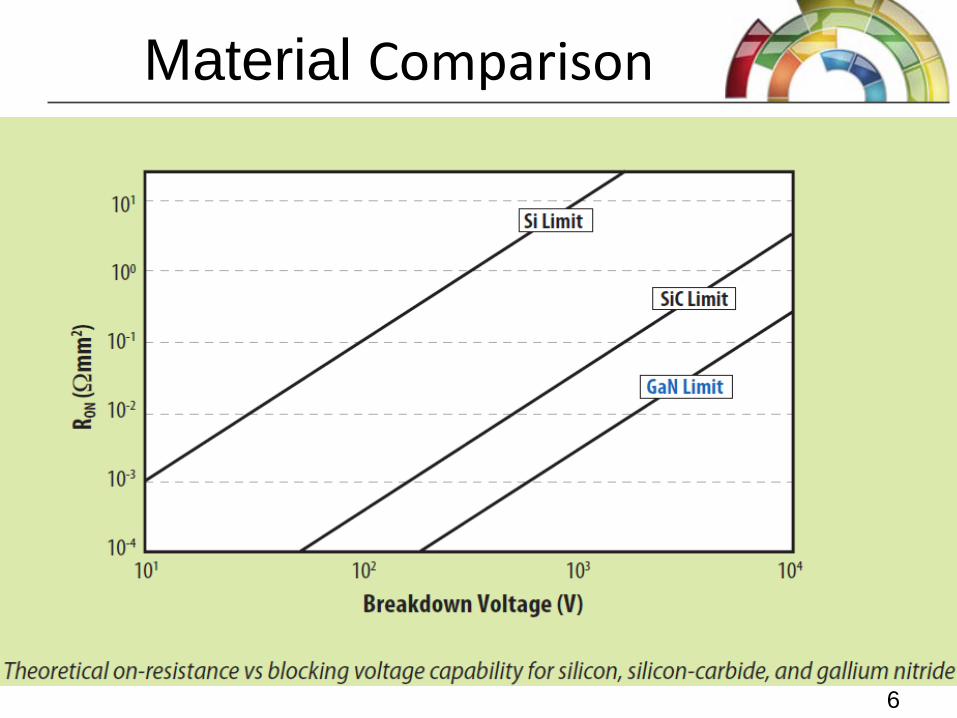
Material Comparison
6
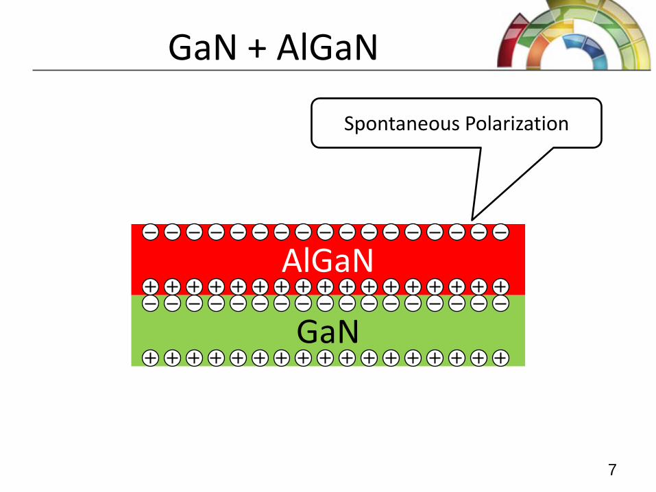
GaN + AlGaN
7
AlGaN
GaN
Spontaneous Polarization
7
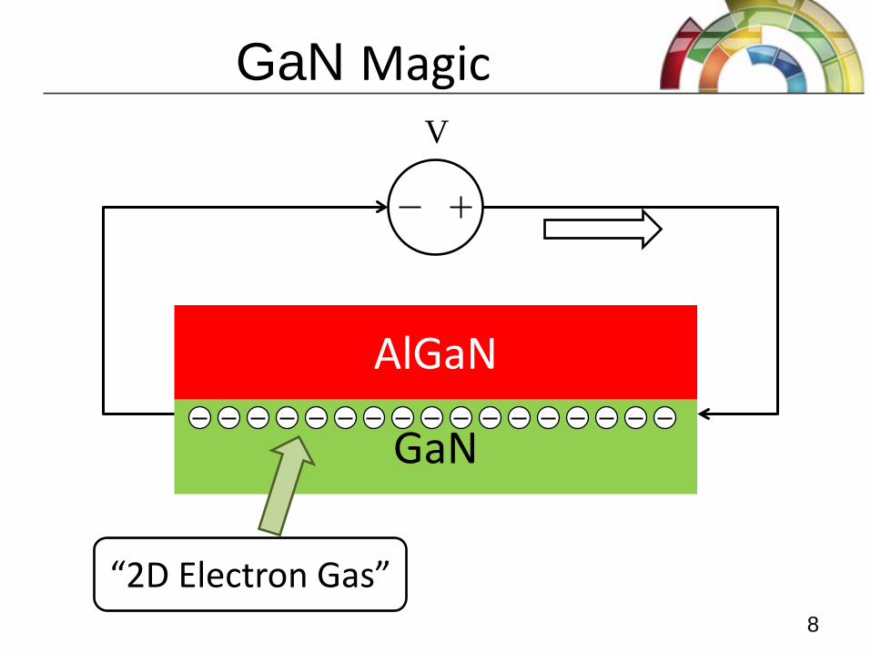
GaN Magic
8
AlGaN
GaN
V
“2D Electron Gas” 8
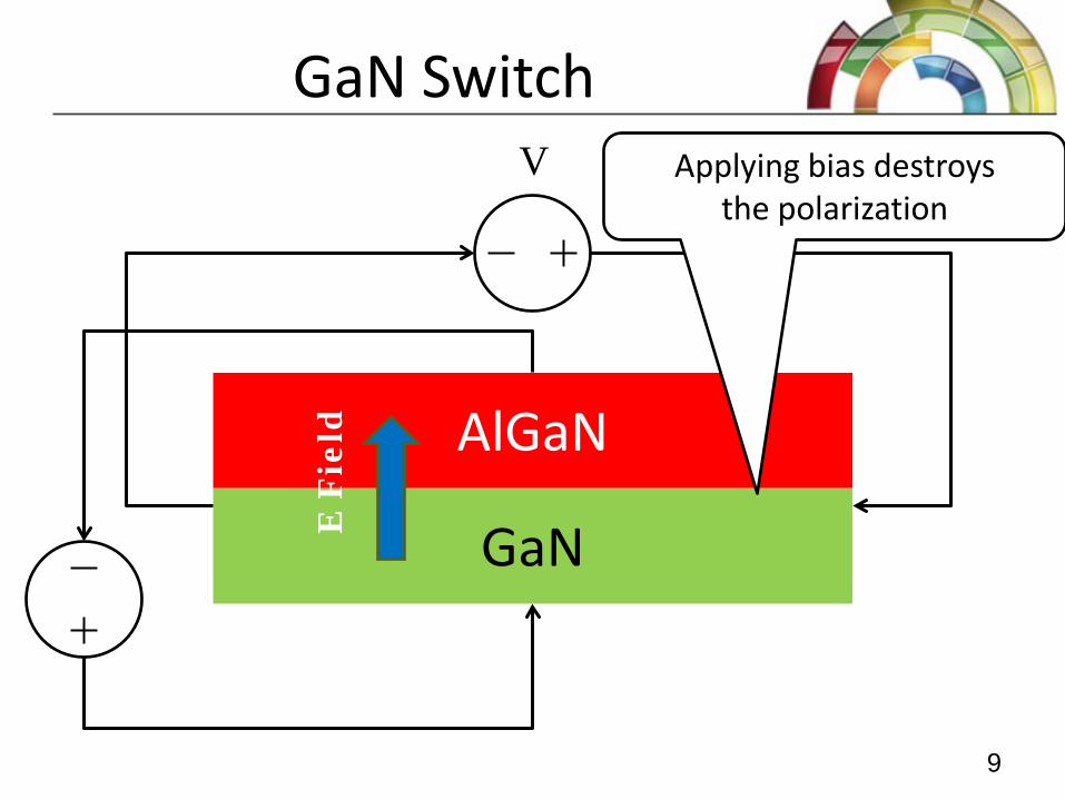
GaN Switch
9
AlGaN
GaN
V Applying bias destroys the polarization
E F
ield
9
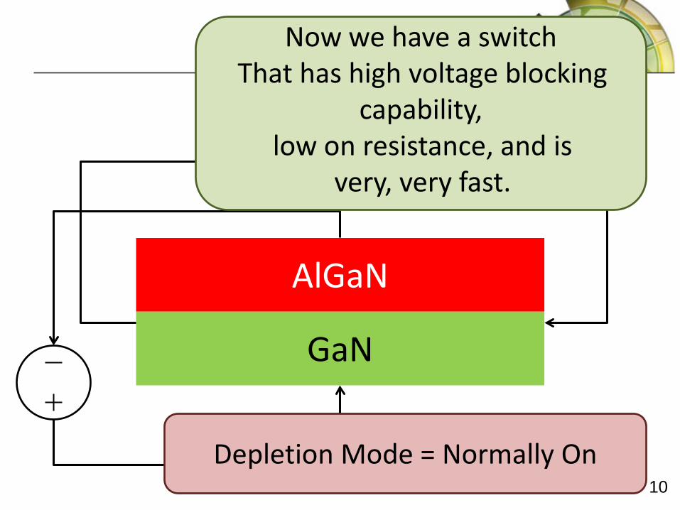
GaN Switch
10
AlGaN
GaN
V
Now we have a switch That has high voltage blocking
capability, low on resistance, and is
very, very fast.
Depletion Mode = Normally On 10
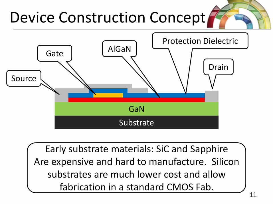
Device Construction Concept
11
GaN Substrate
Drain
Protection Dielectric
Source
Gate AlGaN
Early substrate materials: SiC and Sapphire Are expensive and hard to manufacture. Silicon
substrates are much lower cost and allow fabrication in a standard CMOS Fab.
11
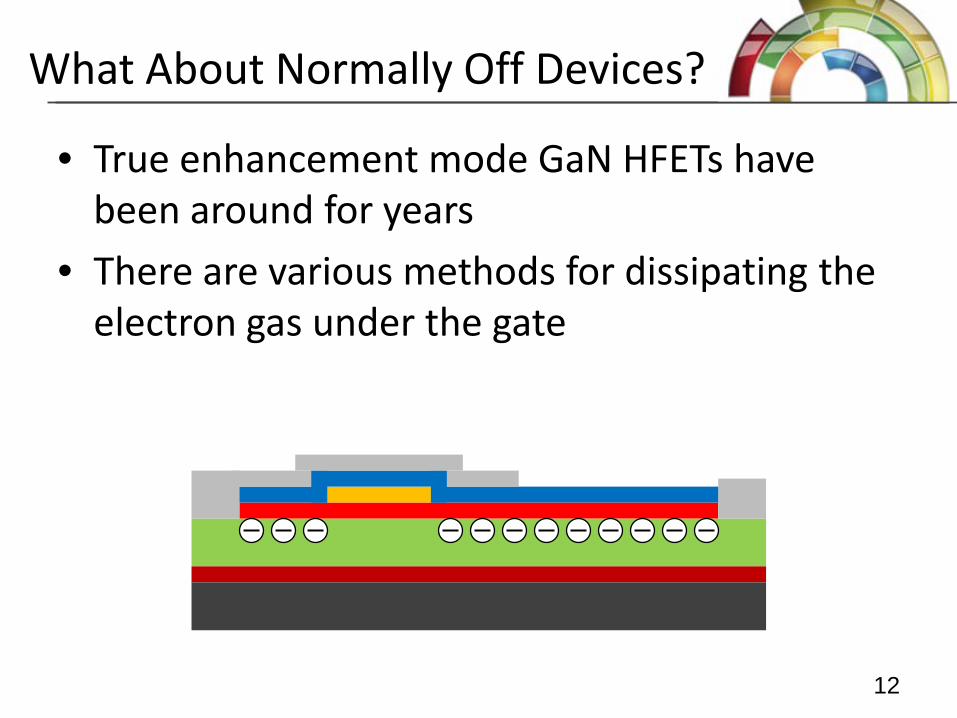
What About Normally Off Devices?
• True enhancement mode GaN HFETs have been around for years
• There are various methods for dissipating the electron gas under the gate
12 12
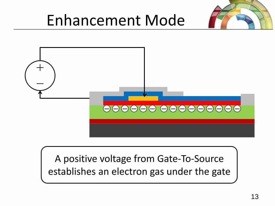
Enhancement Mode
13
A positive voltage from Gate-To-Source establishes an electron gas under the gate
13
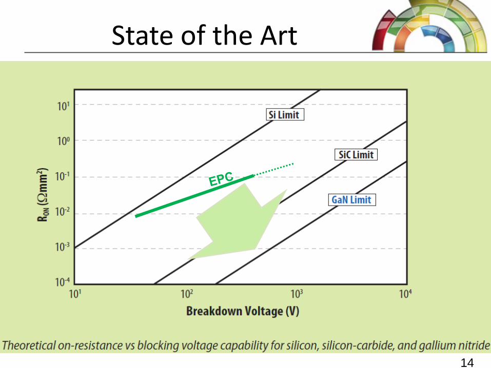
State of the Art
14 14
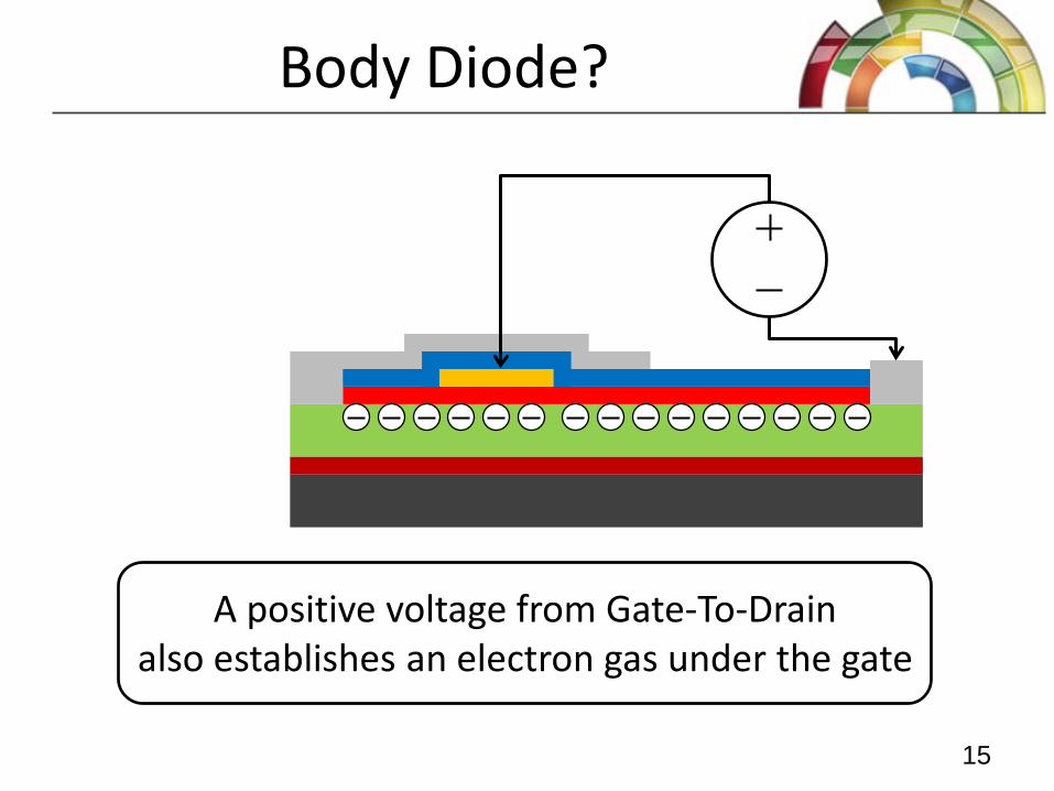
A positive voltage from Gate-To-Drain also establishes an electron gas under the gate
Body Diode?
15 15
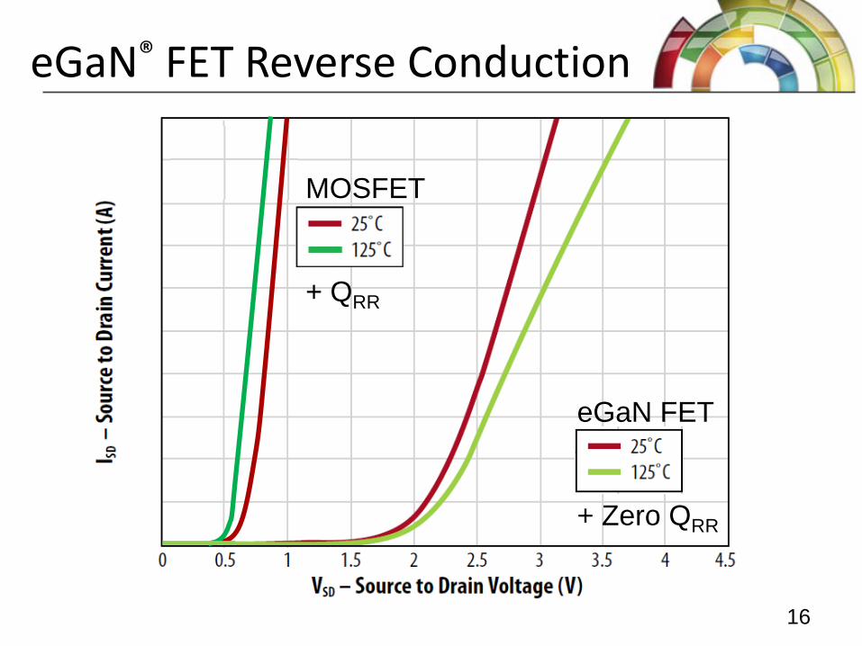
MOSFET + QRR
eGaN FET + Zero QRR
eGaN® FET Reverse Conduction
16 16
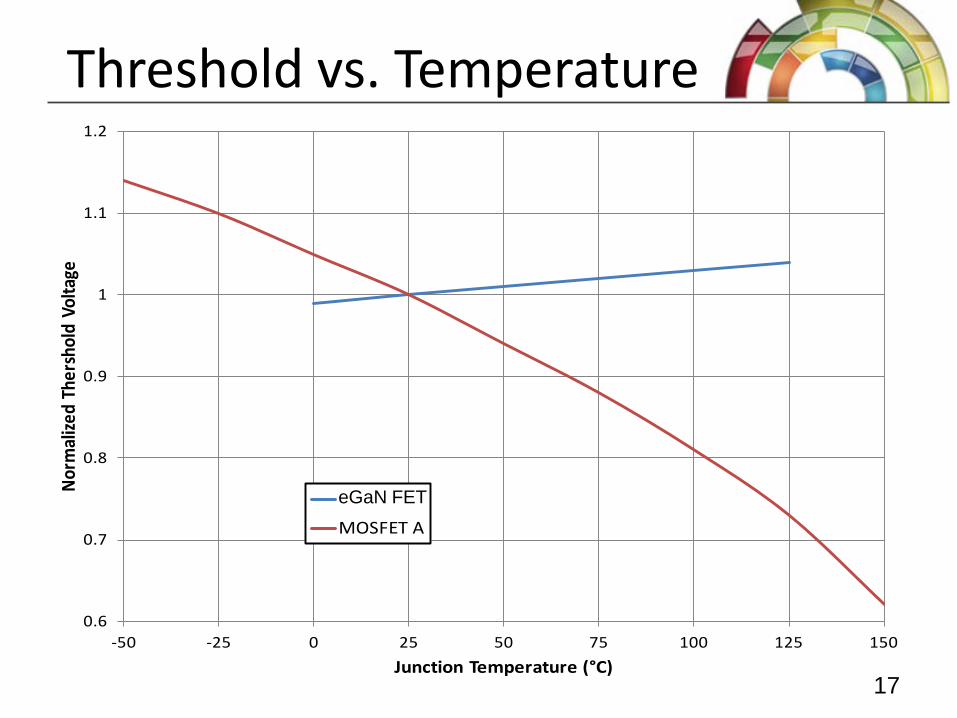
Threshold vs. Temperature
17
0.6
0.7
0.8
0.9
1
1.1
1.2
-50 -25 0 25 50 75 100 125 150
Norm
alize
d Th
ersh
old
Volta
ge
Junction Temperature (°C)
GaN
MOSFET A
eGaN FET
17
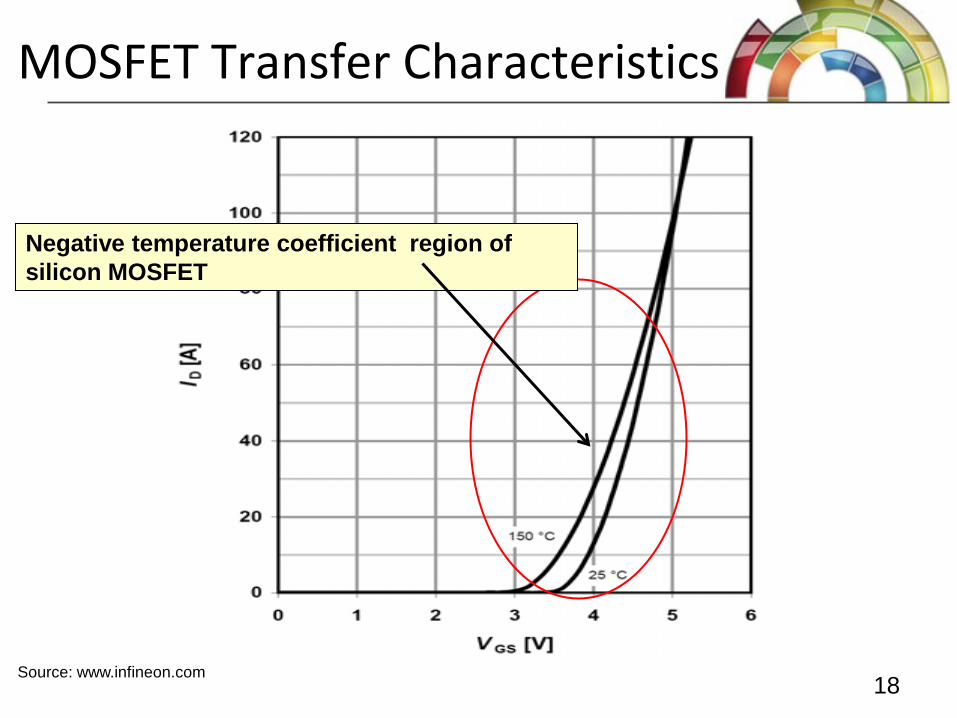
MOSFET Transfer Characteristics
Source: www.infineon.com
Negative temperature coefficient region of silicon MOSFET
18 18
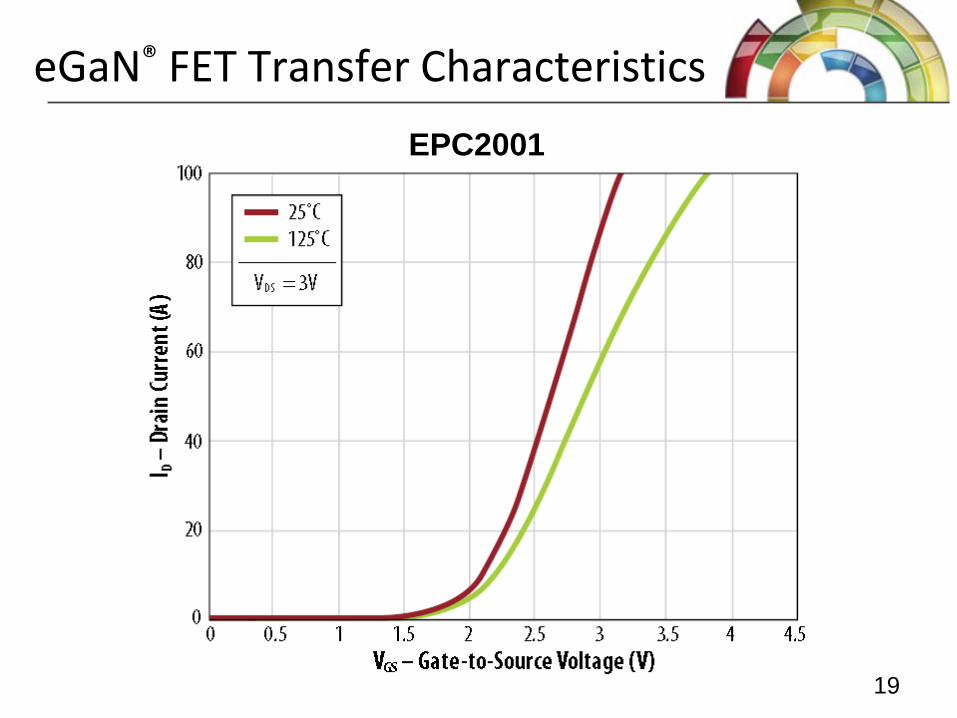
eGaN® FET Transfer Characteristics
19
EPC2001
19
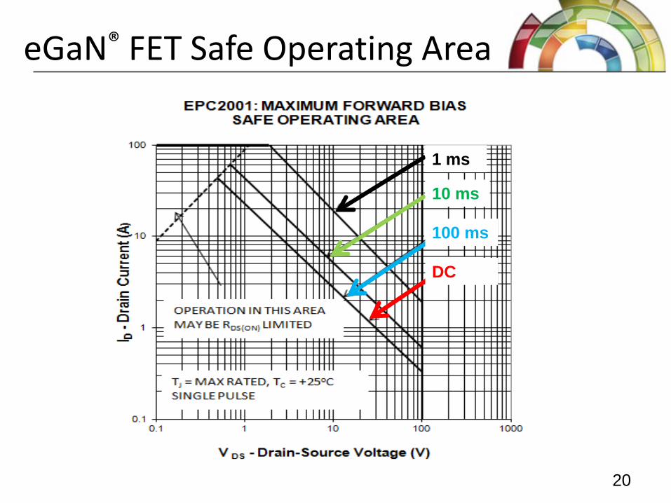
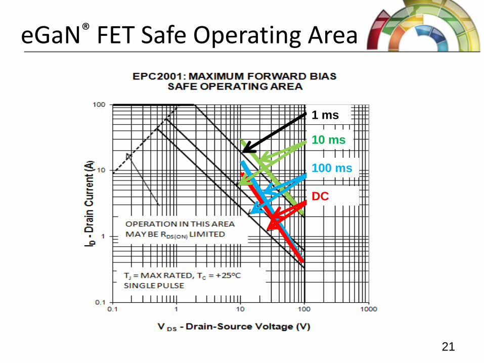
eGaN® FET Safe Operating Area
1 ms
10 ms
100 ms
DC
20
eGaN® FET Safe Operating Area
1 ms
10 ms
100 ms
DC
21
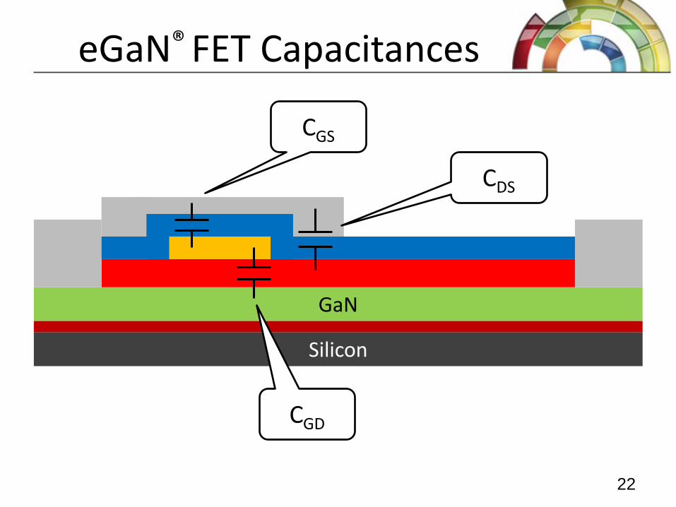
eGaN® FET Capacitances
22
GaN
Silicon
CGD
CDS
CGS
22
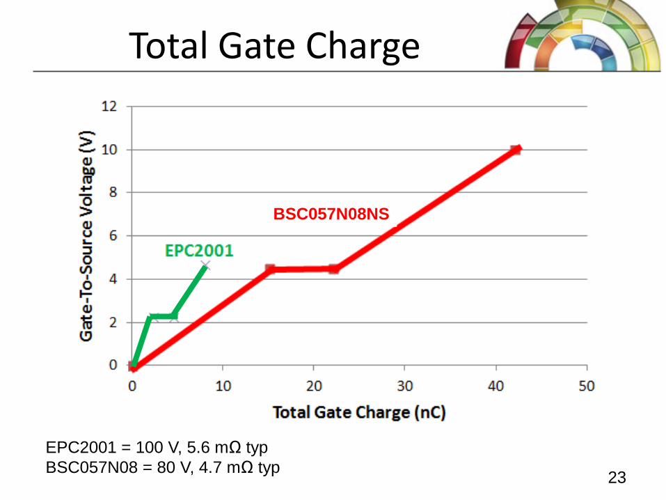
Total Gate Charge
23
EPC2001 = 100 V, 5.6 mΩ typ BSC057N08 = 80 V, 4.7 mΩ typ 23
BSC057N08NS
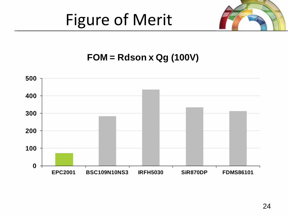
Figure of Merit
24
0
100
200
300
400
500
EPC2001 BSC109N10NS3 IRFH5030 SiR870DP FDMS86101
FOM = Rdson x Qg (100V)
24
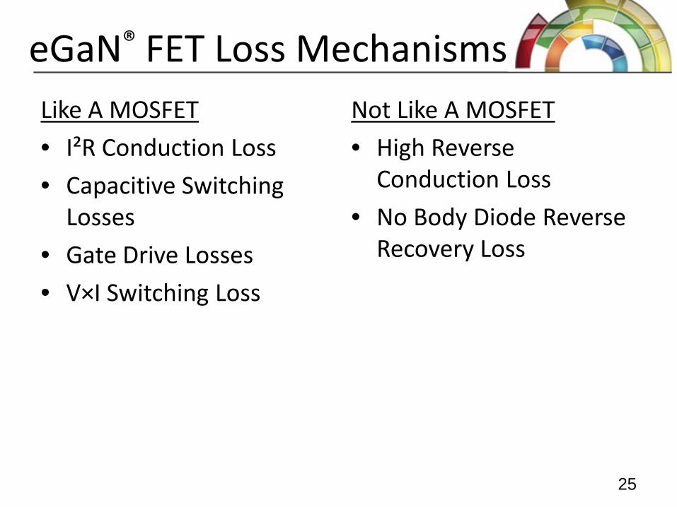
Like A MOSFET • I²R Conduction Loss • Capacitive Switching
Losses • Gate Drive Losses • V×I Switching Loss
Not Like A MOSFET • High Reverse
Conduction Loss • No Body Diode Reverse
Recovery Loss
25 25
eGaN® FET Loss Mechanisms
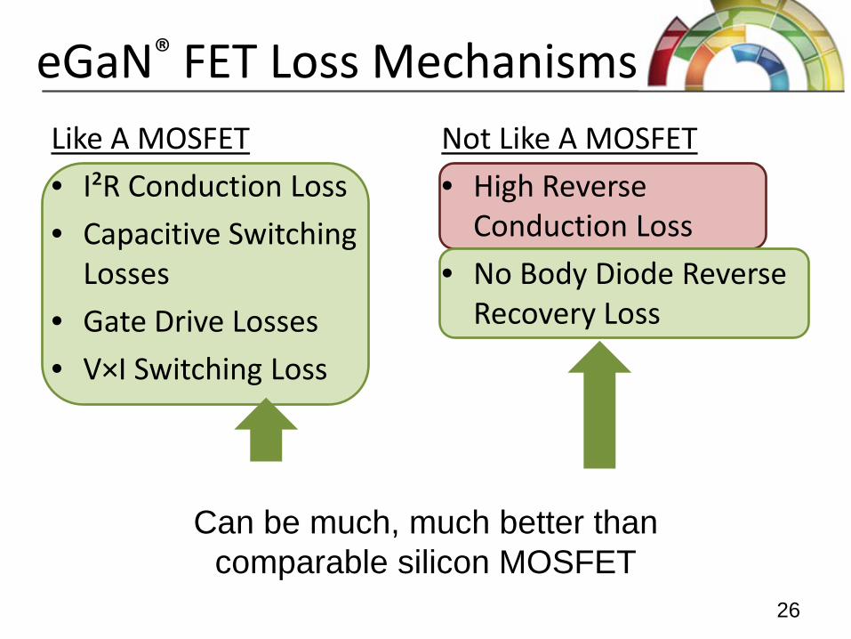
Like A MOSFET • I²R Conduction Loss • Capacitive Switching
Losses • Gate Drive Losses • V×I Switching Loss
Not Like A MOSFET • High Reverse
Conduction Loss • No Body Diode Reverse
Recovery Loss
eGaN® FET Loss Mechanisms
26
Can be much, much better than comparable silicon MOSFET
26

Package Wish List
• Low parasitic resistance • Low parasitic inductance • Low thermal resistance • Small size • Low cost
27 27
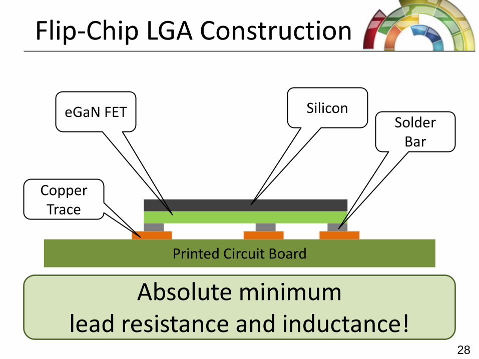
Flip-Chip LGA Construction
28
Printed Circuit Board
Copper Trace
eGaN FET Silicon Solder
Bar
Absolute minimum lead resistance and inductance!
28
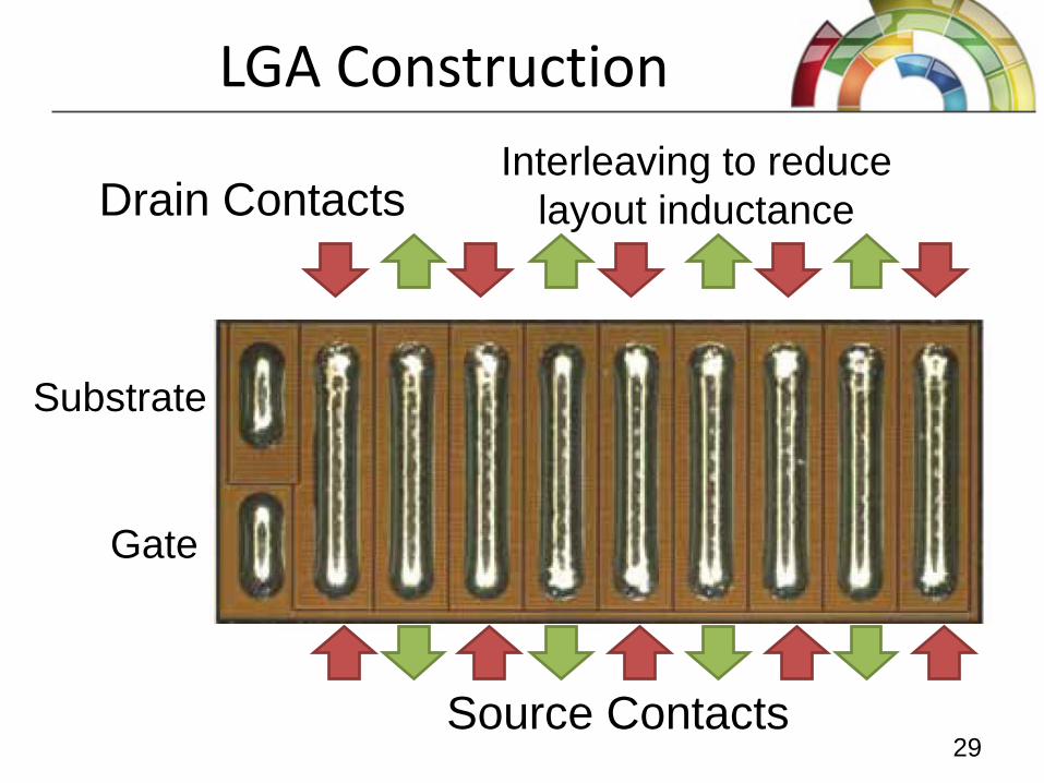
Gate
Substrate
Source Contacts
Drain Contacts
LGA Construction
29
Interleaving to reduce layout inductance
29
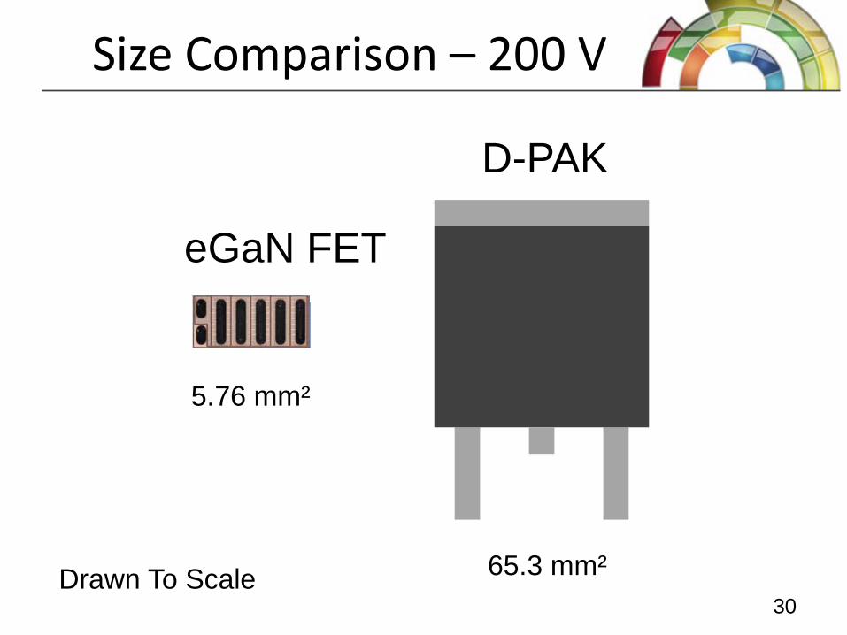
Size Comparison – 200 V
30
D-PAK
eGaN FET
Drawn To Scale
5.76 mm²
65.3 mm² 30
Key Applications
31
• Wireless Power Transmission – GaN Enabled • RF DC-DC “Envelope Tracking” – GaN Enabled • RadHard • Power Over Ethernet • RF Transmission • Network and Server Power Supplies • Point of Load Modules • Energy Efficient Lighting • Class D Audio
31

Design Basics Agenda
• Gate Driver Requirements • Layout • Thermal Management
32 32
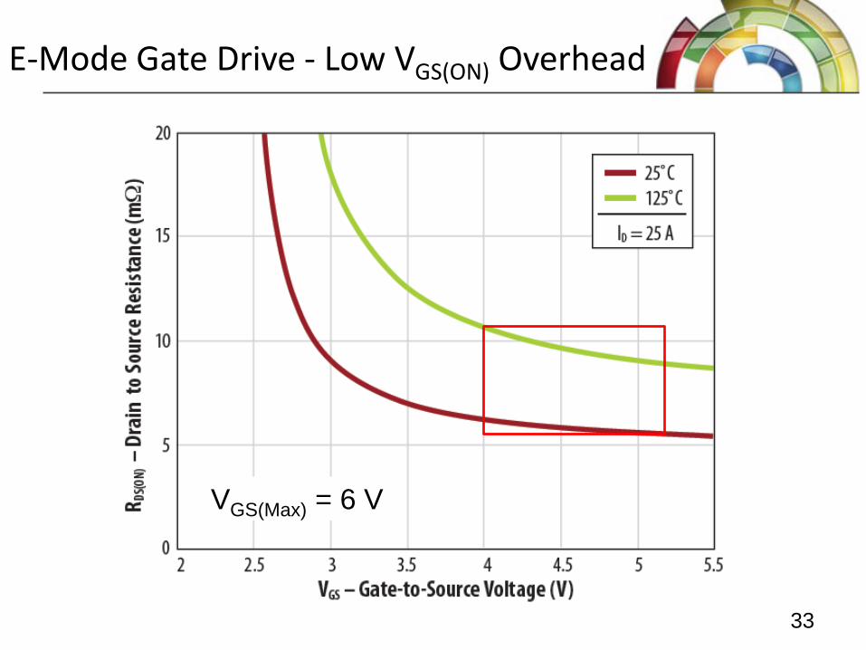
E-Mode Gate Drive - Low VGS(ON) Overhead
33
VGS(Max) = 6 V
33
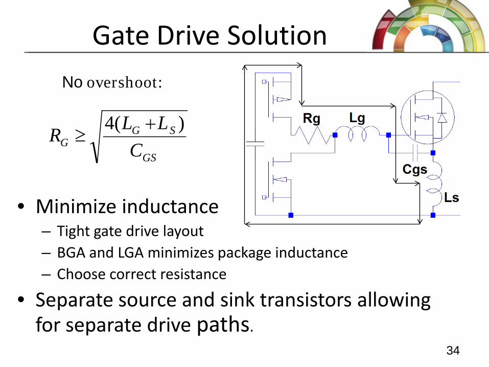
Gate Drive Solution
• Minimize inductance – Tight gate drive layout – BGA and LGA minimizes package inductance – Choose correct resistance
• Separate source and sink transistors allowing for separate drive paths.
34
No overshoot:
GS
SGG C
LLR )(4 +≥
34
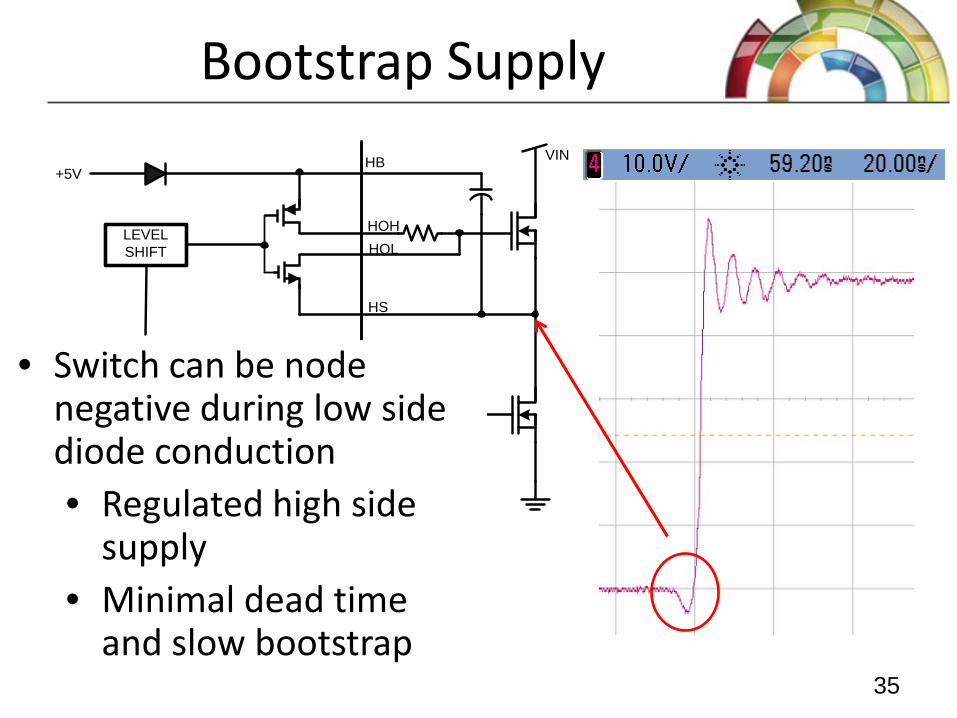
Bootstrap Supply
35
HOHLEVELSHIFT
HB
HS
HOL
+5VVIN
• Switch can be node negative during low side diode conduction • Regulated high side
supply • Minimal dead time
and slow bootstrap 35
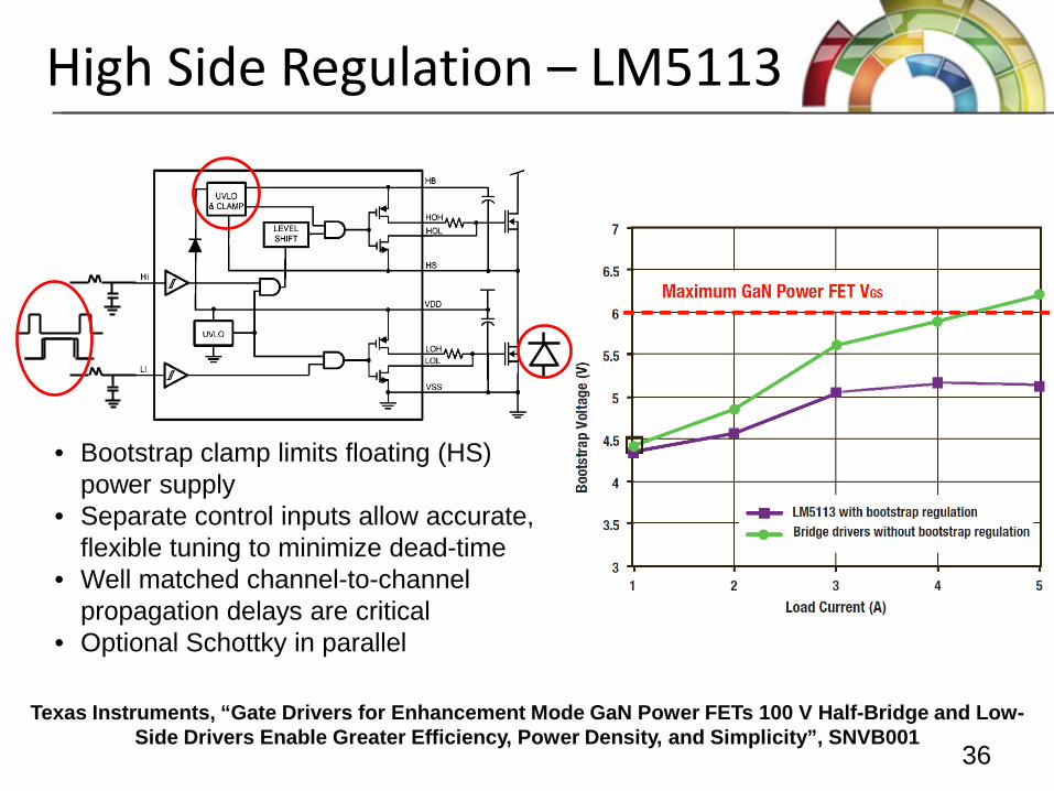
High Side Regulation – LM5113
36
• Bootstrap clamp limits floating (HS) power supply
• Separate control inputs allow accurate, flexible tuning to minimize dead-time
• Well matched channel-to-channel propagation delays are critical
• Optional Schottky in parallel
Texas Instruments, “Gate Drivers for Enhancement Mode GaN Power FETs 100 V Half-Bridge and Low-Side Drivers Enable Greater Efficiency, Power Density, and Simplicity”, SNVB001
36

Layout
37 37
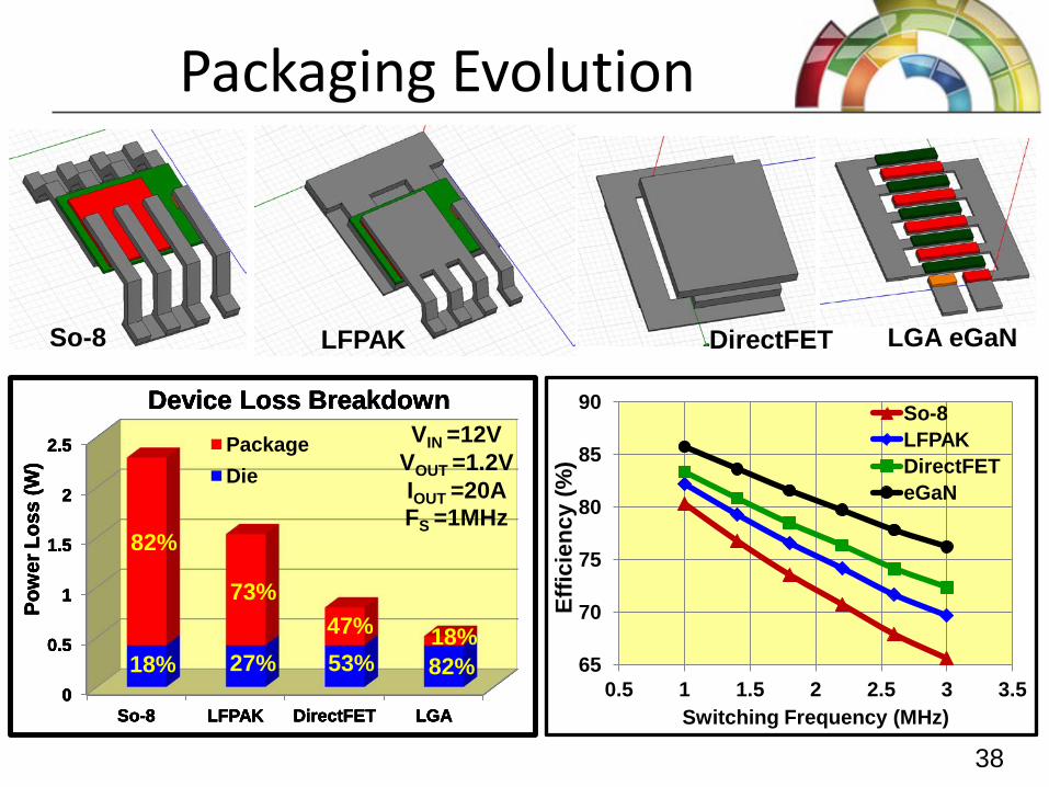
Packaging Evolution
65
70
75
80
85
90
0.5 1 1.5 2 2.5 3 3.5
Effic
ienc
y (%
)
Switching Frequency (MHz)
So-8 LFPAK DirectFET eGaN
0
0.5
1
1.5
2
2.5
So-8 LFPAK DirectFET LGA
Pow
er L
oss
(W)
Device Loss Breakdown Package Die
18%
82%
VIN =12V VOUT =1.2V IOUT =20A FS =1MHz
0
0.5
1
1.5
2
2.5
So-8 LFPAK DirectFET LGA
Pow
er L
oss
(W)
Device Loss Breakdown Package Die
18%
82%
27%
73%
VIN =12V VOUT =1.2V IOUT =20A FS =1MHz
0
0.5
1
1.5
2
2.5
So-8 LFPAK DirectFET LGA
Pow
er L
oss
(W)
Device Loss Breakdown Package Die
18%
82%
27%
73%
53%
47%
VIN =12V VOUT =1.2V IOUT =20A FS =1MHz
0
0.5
1
1.5
2
2.5
So-8 LFPAK DirectFET LGA
Pow
er L
oss
(W)
Device Loss Breakdown Package Die
18%
82%
27%
73%
53%
47%
82% 18%
VIN =12V VOUT =1.2V IOUT =20A FS =1MHz
38
So-8 LFPAK DirectFET LGA eGaN
38
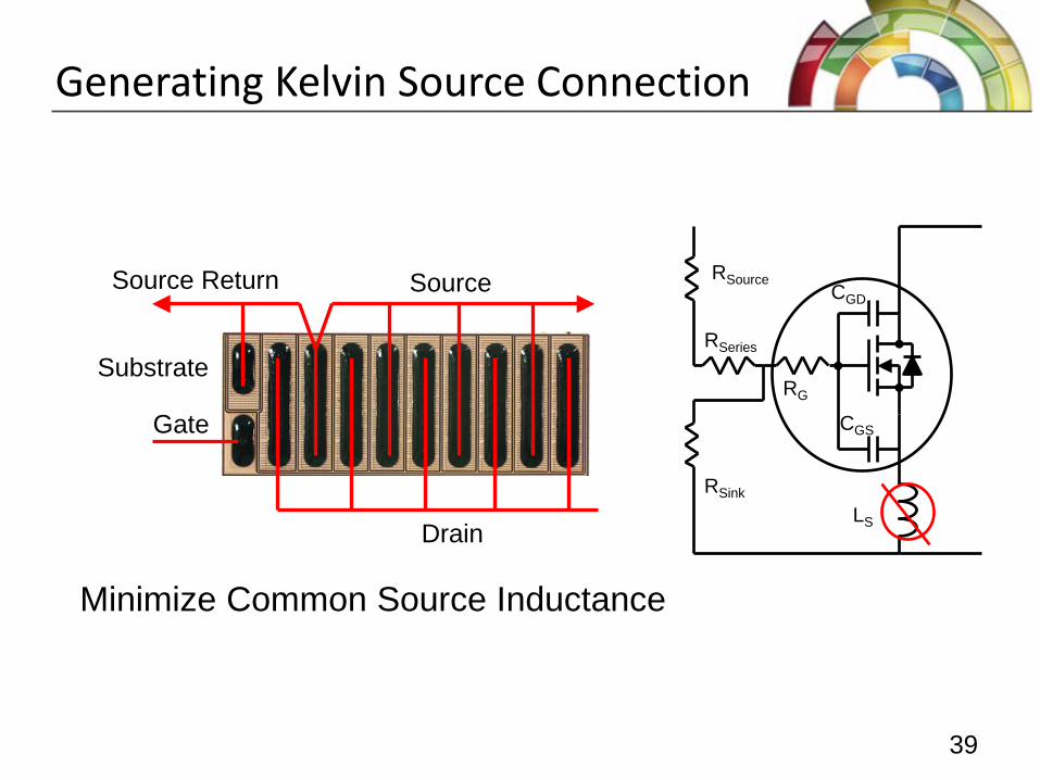
Generating Kelvin Source Connection
39
LS
CGS
CGD
RG
RSink
RSource
RSeries Substrate
Source
Gate
Drain
Minimize Common Source Inductance
39
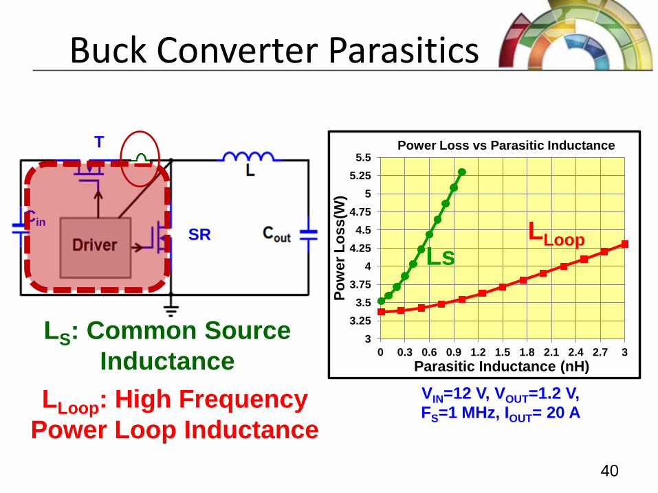
Source Return
3 3.25
3.5 3.75
4 4.25
4.5 4.75
5 5.25
5.5
0 0.3 0.6 0.9 1.2 1.5 1.8 2.1 2.4 2.7 3 Po
wer
Los
s(W
)
Parasitic Inductance (nH)
Power Loss vs Parasitic Inductance
Ls
3 3.25
3.5 3.75
4 4.25
4.5 4.75
5 5.25
5.5
0 0.3 0.6 0.9 1.2 1.5 1.8 2.1 2.4 2.7 3 Po
wer
Los
s(W
)
Parasitic Inductance (nH)
Power Loss vs Parasitic Inductance
Ls LLoop
Cin
T
SR
VIN=12 V, VOUT=1.2 V, FS=1 MHz, IOUT= 20 A
Buck Converter Parasitics
LLoop: High Frequency Power Loop Inductance
40
LS: Common Source Inductance
40
83
84
85
86
87
88
89
90
91
2 4 6 8 10 12 14 16 18 20 22 24
Effic
ienc
y (%
)
Output Current (IOUT)
LLoop≈2.9nH
40V MOSFET
83
84
85
86
87
88
89
90
91
2 4 6 8 10 12 14 16 18 20 22 24
Effic
ienc
y (%
)
Output Current (IOUT)
LLoop≈1.6nH
LLoop≈2.9nH
40V MOSFET
83
84
85
86
87
88
89
90
91
2 4 6 8 10 12 14 16 18 20 22 24
Effic
ienc
y (%
)
Output Current (IOUT)
LLoop≈1.0nH
LLoop≈1.6nH
LLoop≈2.9nH
40V MOSFET
83
84
85
86
87
88
89
90
91
2 4 6 8 10 12 14 16 18 20 22 24
Effic
ienc
y (%
)
Output Current (IOUT)
LLoop≈1.0nH
LLoop≈1.6nH
LLoop≈0.4nH
LLoop≈2.9nH
40V MOSFET
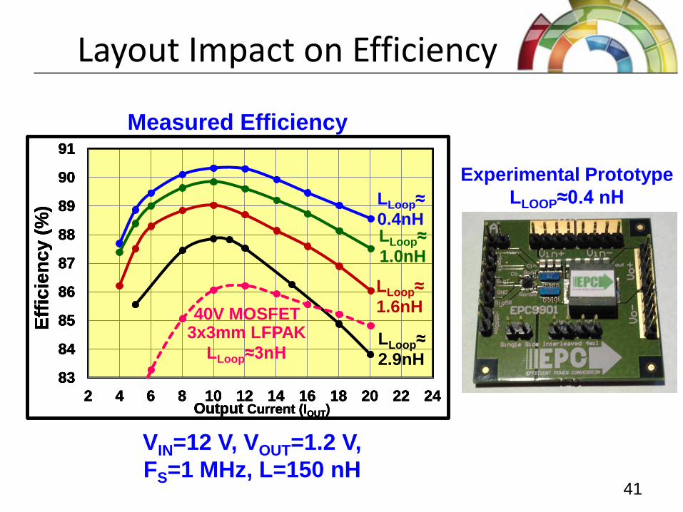
Layout Impact on Efficiency
VIN=12 V, VOUT=1.2 V, FS=1 MHz, L=150 nH
Measured Efficiency
Experimental Prototype LLOOP≈0.4 nH
3x3mm LFPAK LLoop≈3nH
41 41
LLoop≈1.0 nH LLoop ≈ 0.4 nH
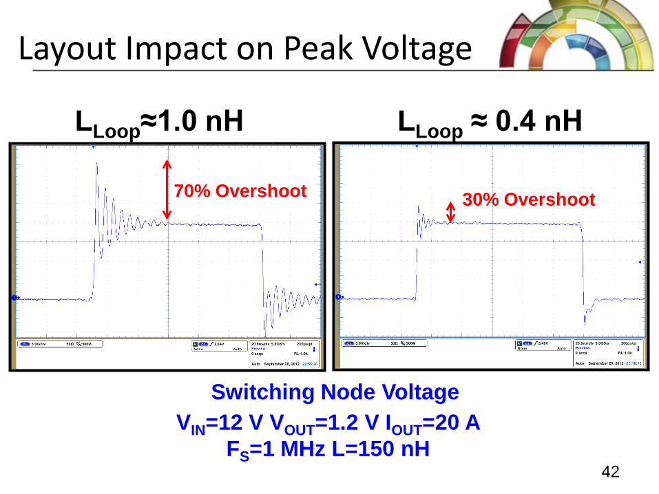
Layout Impact on Peak Voltage
VIN=12 V VOUT=1.2 V IOUT=20 A FS=1 MHz L=150 nH
Switching Node Voltage
70% Overshoot 30% Overshoot
42 42
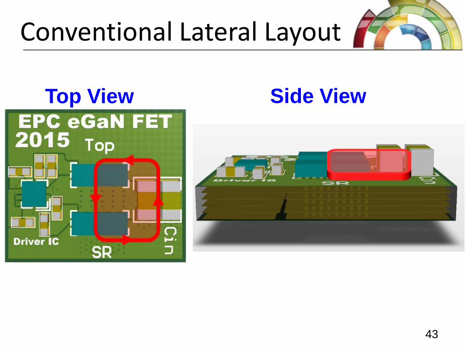
Conventional Lateral Layout
Top View Side View
43 43
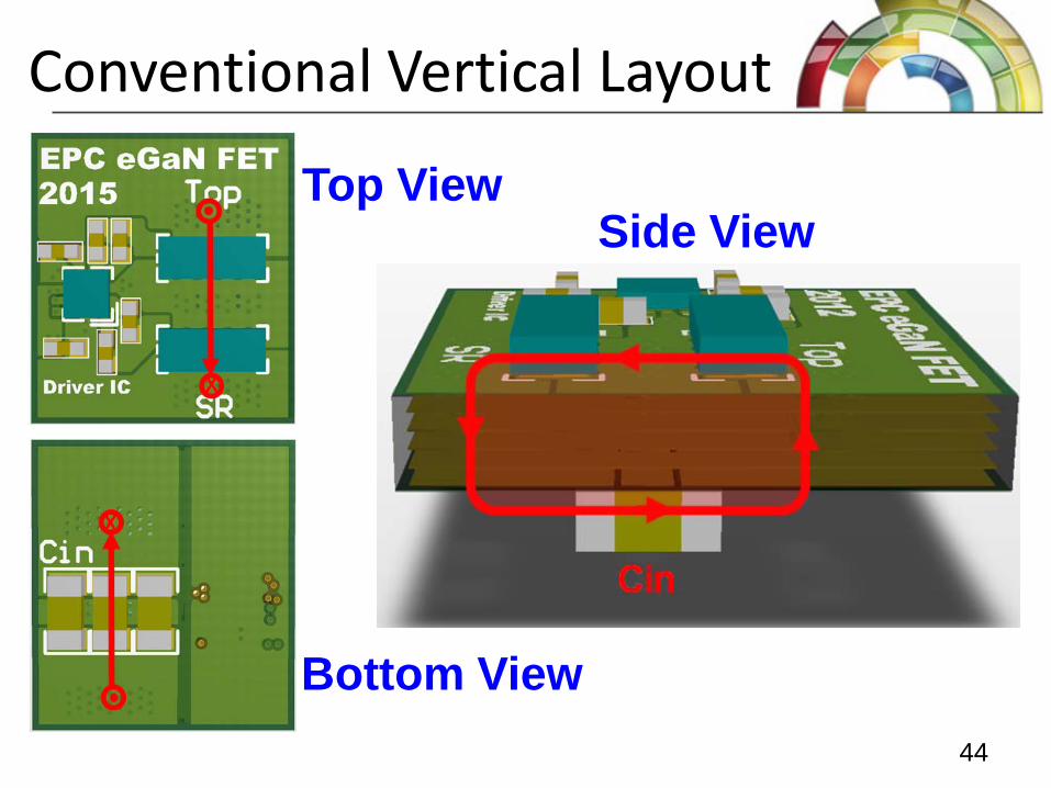
Conventional Vertical Layout
Top View Side View
Bottom View
44 44
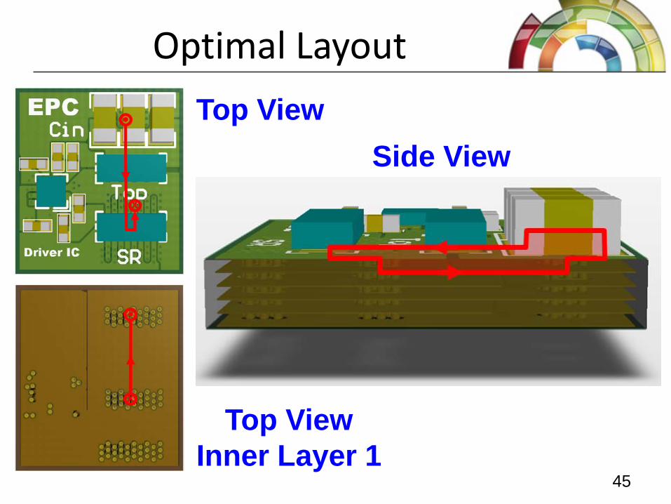
Optimal Layout Top View
Side View
Top View Inner Layer 1
45 45
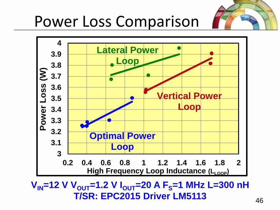
Power Loss Comparison
33.13.23.33.43.53.63.73.83.9
4
0.2 0.4 0.6 0.8 1 1.2 1.4 1.6 1.8 2
Pow
er L
oss
(W)
High Frequency Loop Inductance (LLOOP)
Vertical Power Loop
Lateral Power Loop
Optimal Power Loop
VIN=12 V VOUT=1.2 V IOUT=20 A FS=1 MHz L=300 nH T/SR: EPC2015 Driver LM5113
46 46
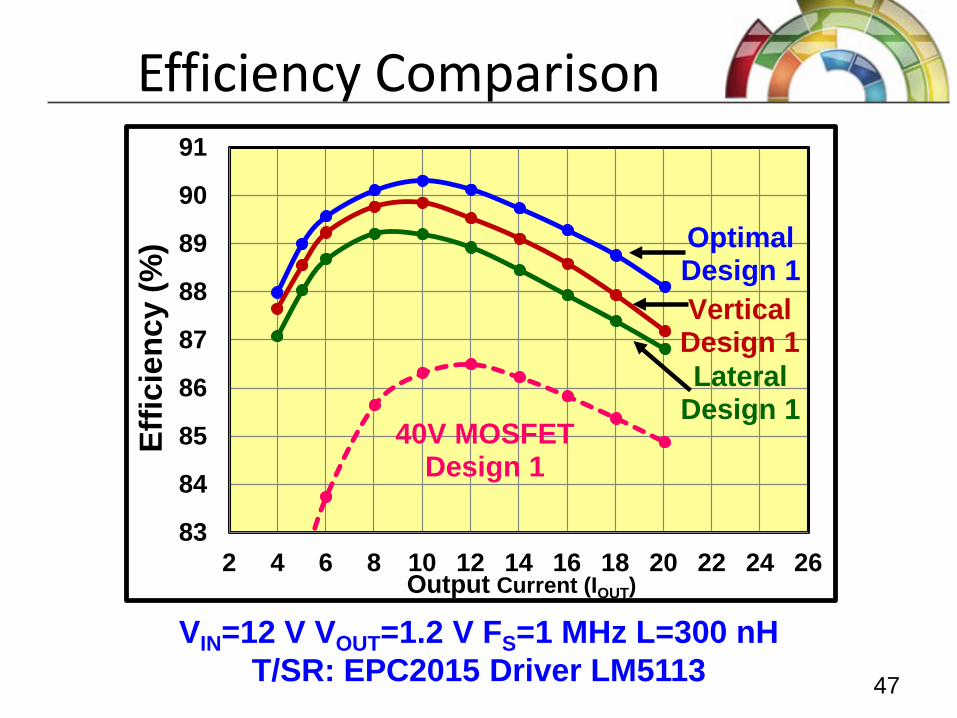
Efficiency Comparison
VIN=12 V VOUT=1.2 V FS=1 MHz L=300 nH T/SR: EPC2015 Driver LM5113
83
84
85
86
87
88
89
90
91
2 4 6 8 10 12 14 16 18 20 22 24 26
Effic
ienc
y (%
)
Output Current (IOUT)
40V MOSFETDesign 1
Vertical Design 1Lateral
Design 1
Optimal Design 1
47 47
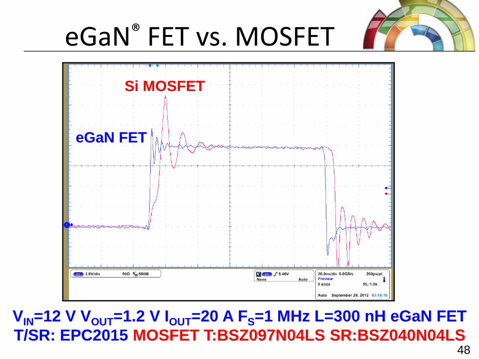
eGaN® FET vs. MOSFET
VIN=12 V VOUT=1.2 V IOUT=20 A FS=1 MHz L=300 nH eGaN FET T/SR: EPC2015 MOSFET T:BSZ097N04LS SR:BSZ040N04LS
Si MOSFET
eGaN FET
48 48
Layout Summary eGaN FETs improve performance in high switching frequency converters • CSI is a critical component for maximizing
switching performance • Gate drive loop inductance limits switching speed • Optimizing power loop inductance improves
efficiency and minimizes voltage overshoot • Current measurements affect performance • Voltage measurements are bandwidth limited • Reduced ringing reduces EMI 49
49

Thermal Management
50 50
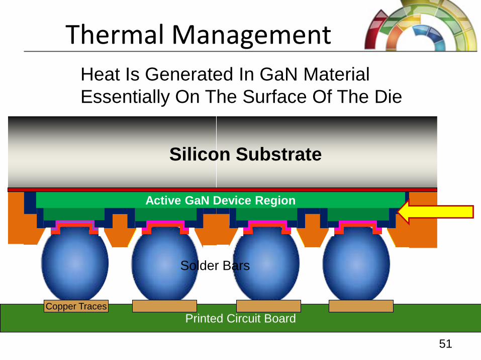
Thermal Management
51
Heat Is Generated In GaN Material Essentially On The Surface Of The Die
Printed Circuit Board Copper Traces
Silicon Substrate
Active GaN Device Region
Solder Bars
51
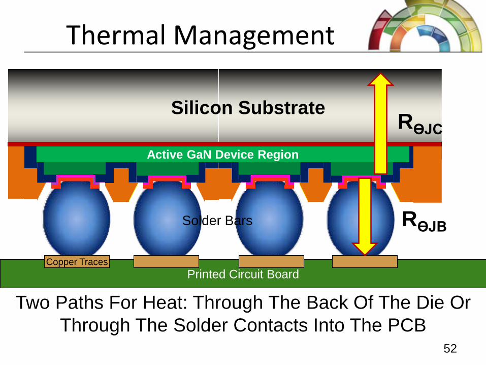
Thermal Management
52
Two Paths For Heat: Through The Back Of The Die Or Through The Solder Contacts Into The PCB
Printed Circuit Board Copper Traces
Silicon Substrate
Active GaN Device Region
Solder Bars RƟJB
RƟJC
52
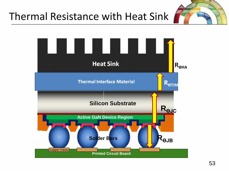
Thermal Resistance with Heat Sink
53
Printed Circuit Board Copper Traces
Silicon Substrate
Active GaN Device Region
Solder Bars RƟJB
RƟJC
53
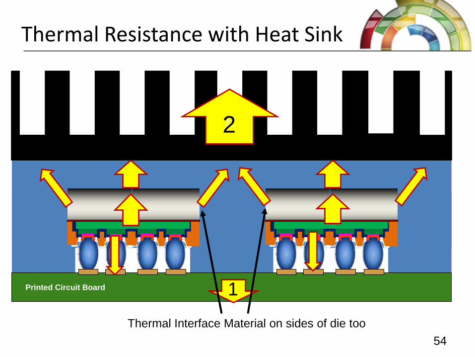
Thermal Resistance with Heat Sink
54
Printed Circuit Board
22 2
1
Thermal Interface Material on sides of die too 54
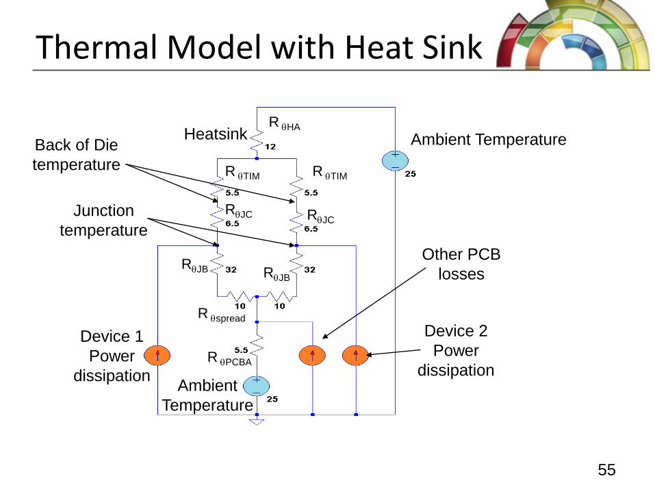
Thermal Model with Heat Sink
55
Ambient Temperature
Ambient Temperature
Device 2 Power
dissipation
Device 1 Power
dissipation
Heatsink
Junction temperature
RθJC
RθJB
RθJC
RθJB
R θTIM R θTIM
R θPCBA
R θspread
Back of Die temperature
Other PCB losses
R θHA
55
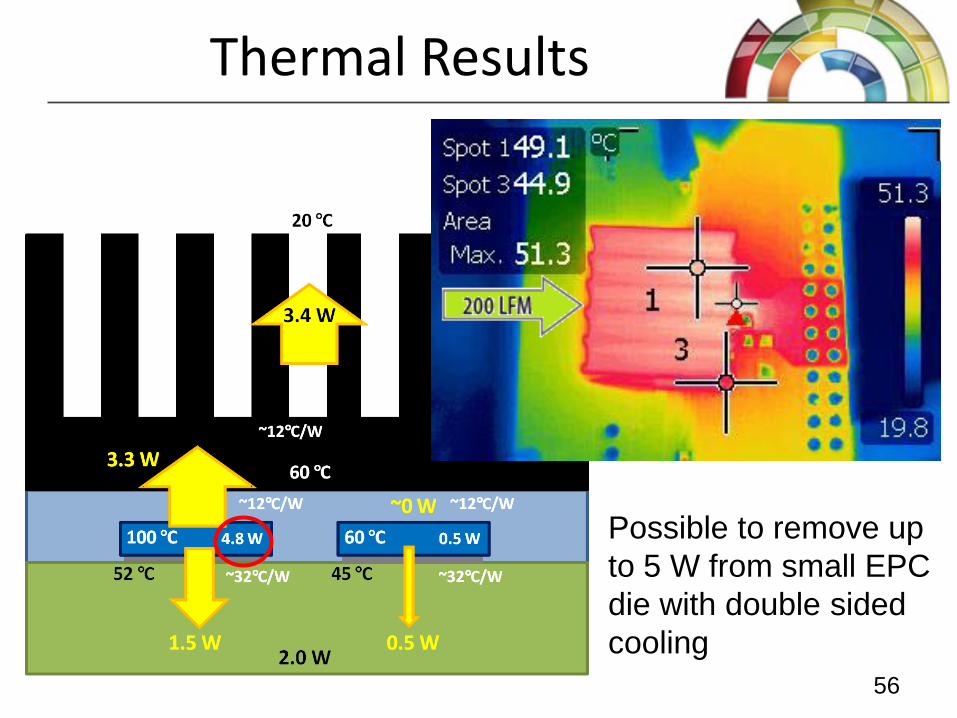
Thermal Results
Possible to remove up to 5 W from small EPC die with double sided cooling
56

Design Example Agenda • Hard Switched Circuits
– Buck Converter – Isolated Full Bridge – Envelope Tracking
• Resonant Circuits – Intermediate Bus Converter
57 57

Buck Converters
58
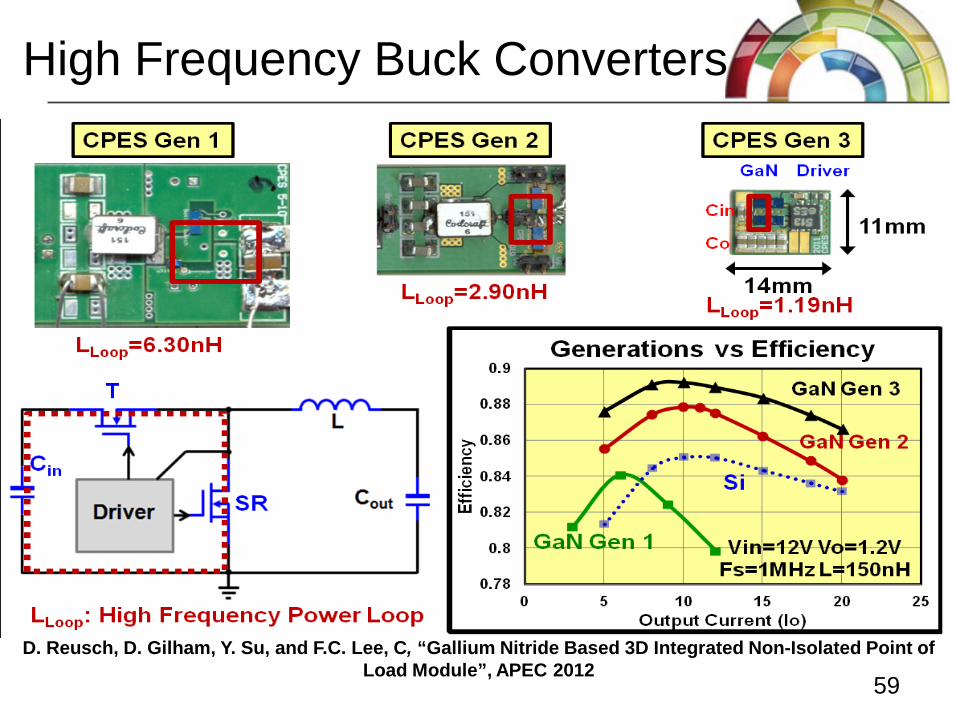
D. Reusch, D. Gilham, Y. Su, and F.C. Lee, C, “Gallium Nitride Based 3D Integrated Non-Isolated Point of Load Module”, APEC 2012
High Frequency Buck Converters
59
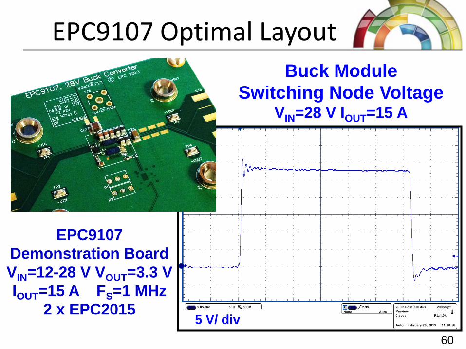
EPC9107 Optimal Layout
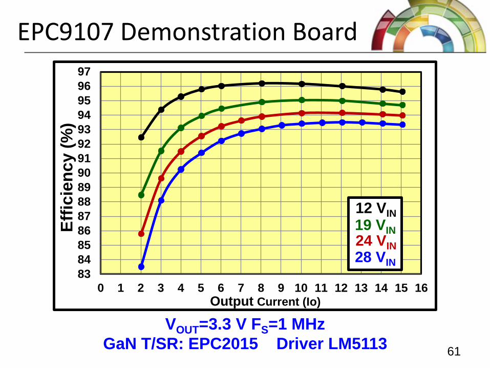
EPC9107 Demonstration Board VIN=12-28 V VOUT=3.3 V IOUT=15 A FS=1 MHz
2 x EPC2015 5 V/ div
Buck Module Switching Node Voltage
VIN=28 V IOUT=15 A
60
838485868788899091929394959697
0 1 2 3 4 5 6 7 8 9 10 11 12 13 14 15 16
Effic
ienc
y (%
)
Output Current (Io)
28 VIN
12 VIN19 VIN24 VIN
VOUT=3.3 V FS=1 MHz GaN T/SR: EPC2015 Driver LM5113
EPC9107 Demonstration Board
61

Isolated Full Bridge
62
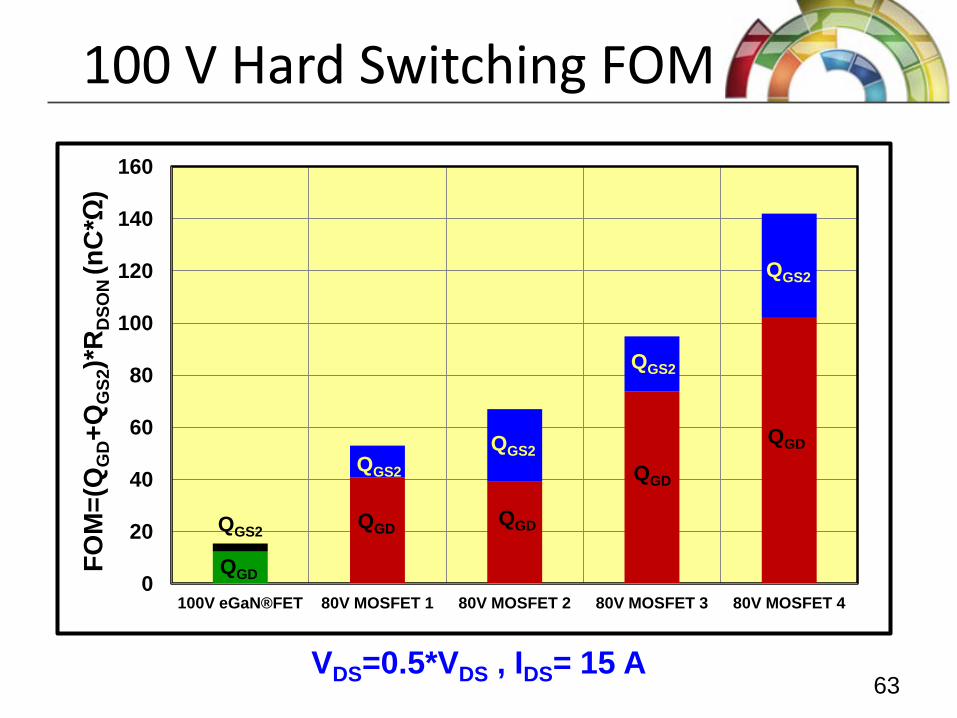
100 V Hard Switching FOM
VDS=0.5*VDS , IDS= 15 A
0
20
40
60
80
100
120
140
160
100V eGaN®FET 80V MOSFET 1 80V MOSFET 2 80V MOSFET 3 80V MOSFET 4
FOM
=(Q
GD+Q
GS2
)*R
DSO
N (n
C*Ω
)
QGD
QGD QGD
QGD QGD
QGS2
QGS2 QGS2
QGS2
QGS2
63 63
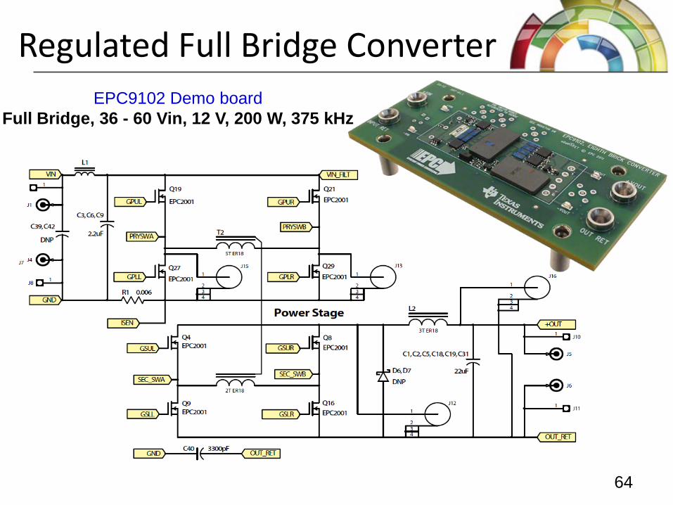
Regulated Full Bridge Converter EPC9102 Demo board
Full Bridge, 36 - 60 Vin, 12 V, 200 W, 375 kHz
64 64
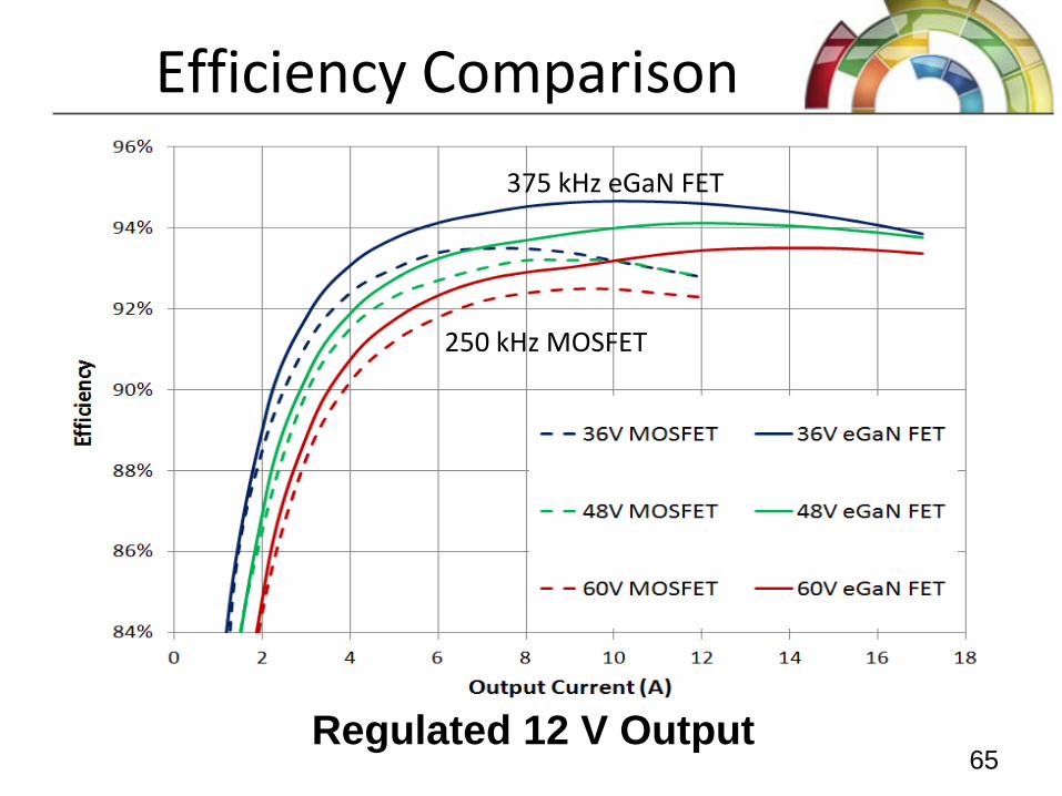
250 kHz MOSFET
375 kHz eGaN FET
Regulated 12 V Output
Efficiency Comparison
65 65
Brick Converter Summary • Topologies varied • Optimization as important as device selection • Efficiency is key to power density
• Maximum power loss is fixed. • Good comparison requires identical designs • Given topology, eGaN FETs will outperform
MOSFETs based on superior FOM
66 66
• World of Radio Frequency Power Amplifiers (RFPA) is changing.
• Increased efficiency driven by: – Improved battery life – Reduced cooling – Reduced size – Lower cost of operation
Overview of Envelope Tracking
67
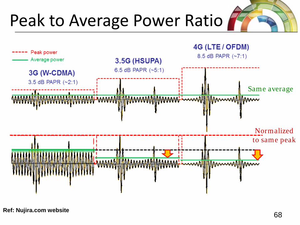
Peak to Average Power Ratio
Ref: Nujira.com website
Same average
Normalized to same peak
68
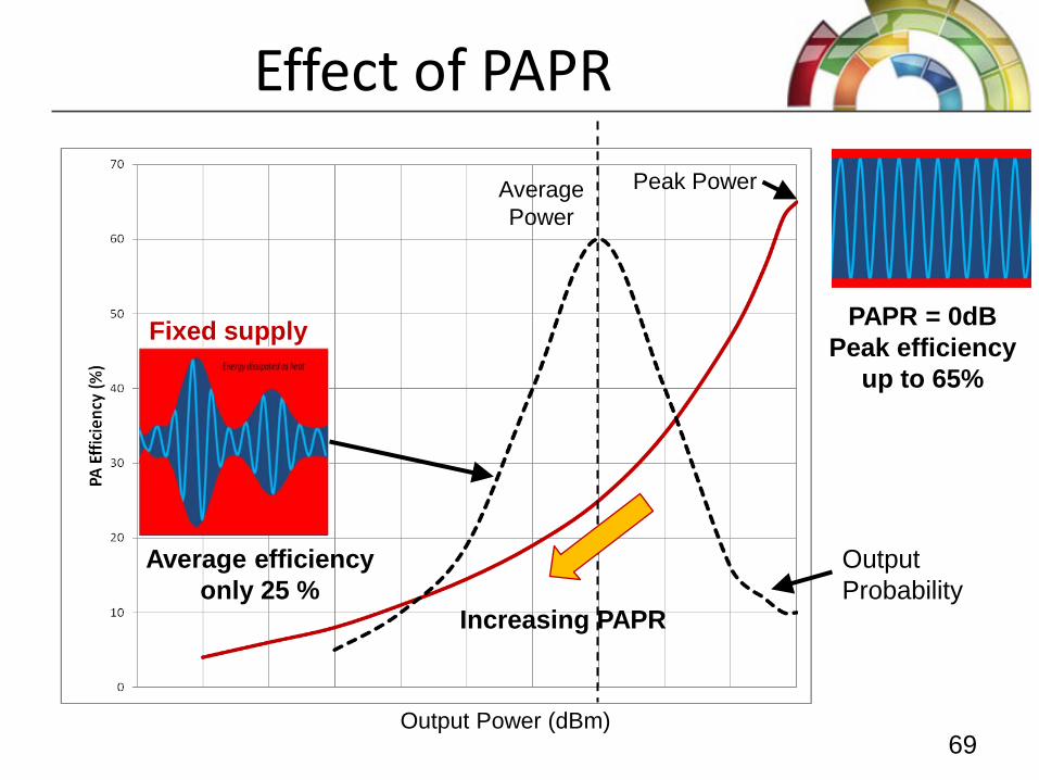
Effect of PAPR
Fixed supply
Peak Power Average Power
Output Power (dBm)
Output Probability
Average efficiency only 25 %
PAPR = 0dB Peak efficiency
up to 65%
Increasing PAPR
69
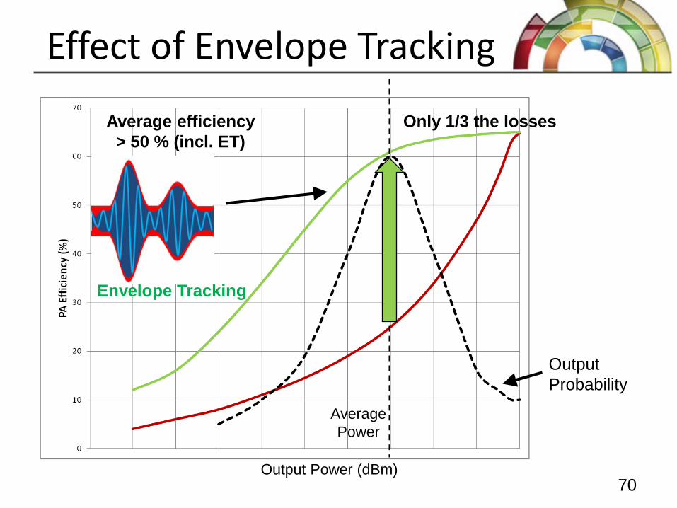
Effect of Envelope Tracking
Output Power (dBm)
Average efficiency > 50 % (incl. ET)
Only 1/3 the losses
Average Power
Output Probability
Envelope Tracking
70
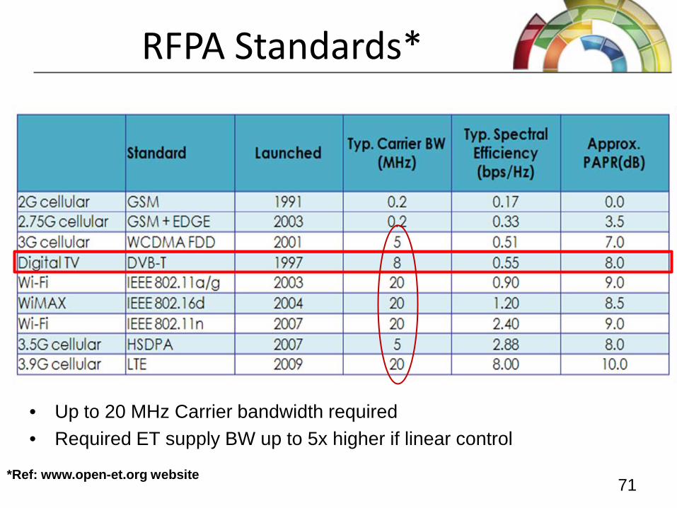
RFPA Standards*
*Ref: www.open-et.org website
• Up to 20 MHz Carrier bandwidth required • Required ET supply BW up to 5x higher if linear control
71
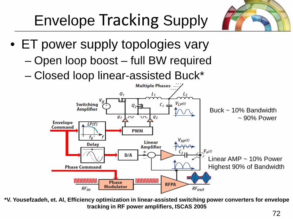
• ET power supply topologies vary – Open loop boost – full BW required – Closed loop linear-assisted Buck*
Envelope Tracking Supply
Buck ~ 10% Bandwidth ~ 90% Power
Linear AMP ~ 10% Power Highest 90% of Bandwidth
*V. Yousefzadeh, et. Al, Efficiency optimization in linear-assisted switching power converters for envelope tracking in RF power amplifiers, ISCAS 2005
72
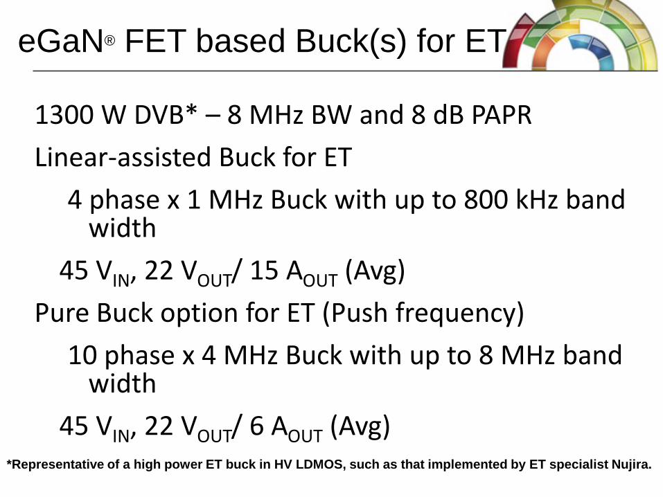
1300 W DVB* – 8 MHz BW and 8 dB PAPR Linear-assisted Buck for ET
4 phase x 1 MHz Buck with up to 800 kHz band width
45 VIN, 22 VOUT/ 15 AOUT (Avg) Pure Buck option for ET (Push frequency)
10 phase x 4 MHz Buck with up to 8 MHz band width
45 VIN, 22 VOUT/ 6 AOUT (Avg)
eGaN® FET based Buck(s) for ET
*Representative of a high power ET buck in HV LDMOS, such as that implemented by ET specialist Nujira.
73
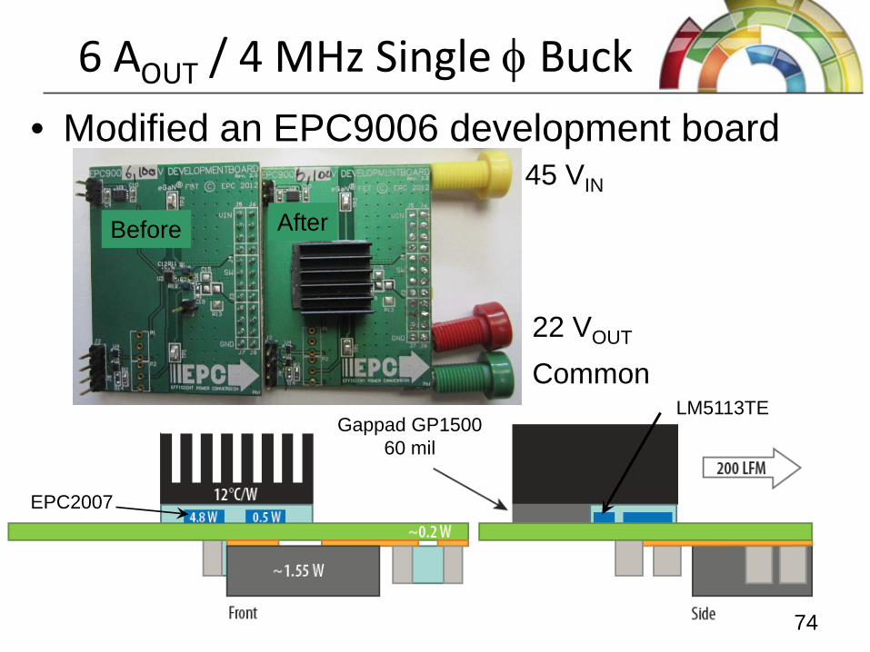
• Modified an EPC9006 development board
6 AOUT / 4 MHz Single φ Buck
45 VIN
22 VOUT
Common LM5113TE
EPC2007
Before After
Gappad GP1500 60 mil
74
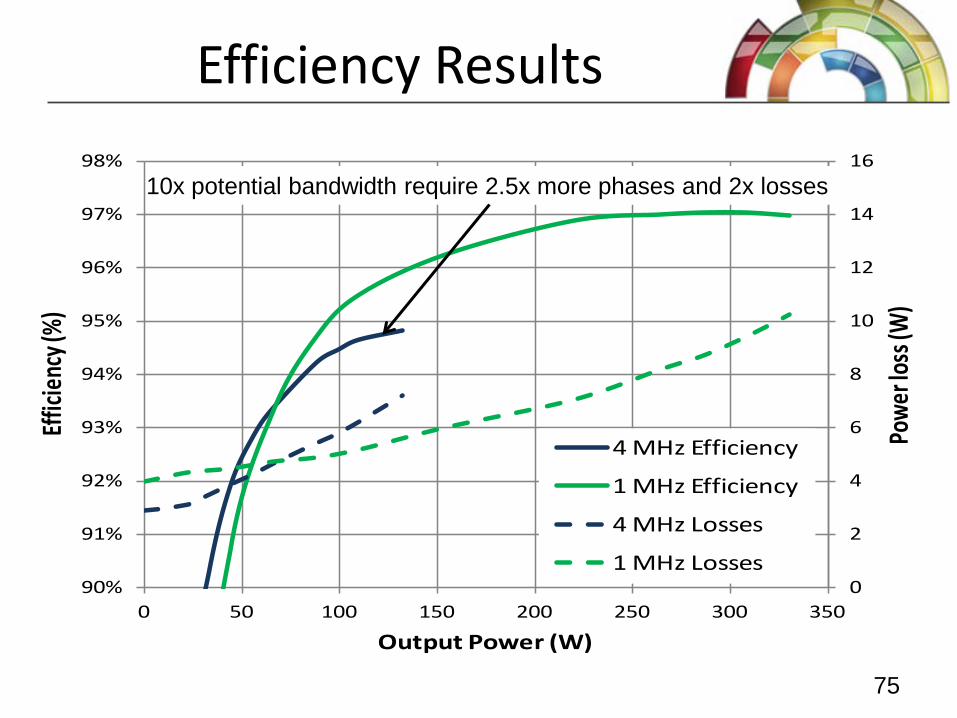
Efficiency Results
0
2
4
6
8
10
12
14
16
90%
91%
92%
93%
94%
95%
96%
97%
98%
0 50 100 150 200 250 300 350
Powe
r loss
(W)
Effici
ency
(%)
Output Power (W)
4 MHz Efficiency
1 MHz Efficiency
4 MHz Losses
1 MHz Losses
10x potential bandwidth require 2.5x more phases and 2x losses
75

Loss Breakdown
1 MHz EPC9002 4 MHz EPC9006 Future die size optimization possible
EPC2001
EPC2001
EPC2007
EPC2007
76 76
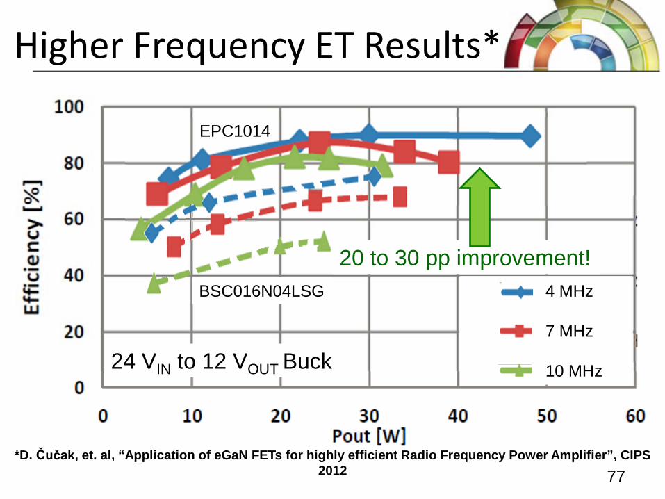
Higher Frequency ET Results*
BSC016N04LSG 4 MHz 7 MHz 10 MHz
*D. Čučak, et. al, “Application of eGaN FETs for highly efficient Radio Frequency Power Amplifier”, CIPS 2012
24 VIN to 12 VOUT Buck
EPC1014
20 to 30 pp improvement!
77
Envelope Tracking Summary • eGaN FETs are an enabling technology for ET
– Low charge reduces delay and switching times – Thermally possible - with double sided cooling
• Results are representative, but not optimized – Improve inductor selection – Improve thermal design – Reduce high side peak device temp by reducing low
side device size to reduce QOSS losses
• Power and # of phases application specific
78 78
Resonant Converters
79
80 80
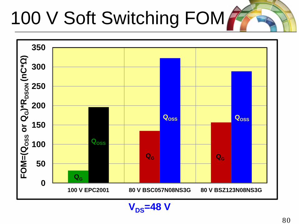
100 V Soft Switching FOM
VDS=48 V
0
50
100
150
200
250
300
350
100 V EPC2001 80 V BSC057N08NS3G 80 V BSZ123N08NS3G
FOM
=(Q
OSS
or Q
G)*
RD
SON
(nC
*Ω)
QG
QG
QOSS
QOSS
QG
QOSS
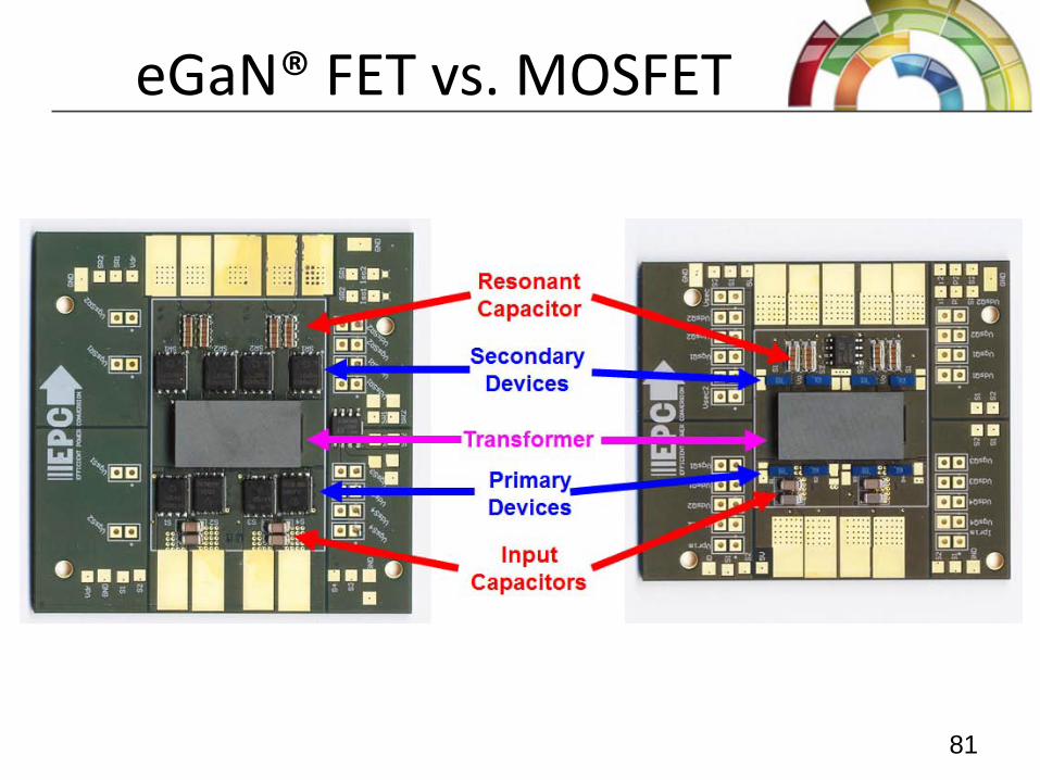
eGaN® FET vs. MOSFET
81
MOSFET VGS MOSFET VDS
eGaN FET VDS
eGaN FET VGS
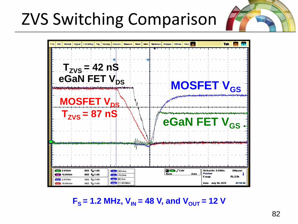
ZVS Switching Comparison
FS = 1.2 MHz, VIN = 48 V, and VOUT = 12 V
TZVS = 87 nS
TZVS = 42 nS
82
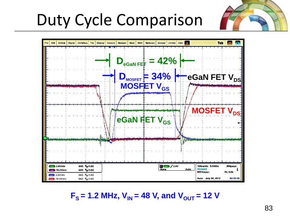
MOSFET VGS
MOSFET VDS
eGaN FET VDS
eGaN FET VGS
Duty Cycle Comparison
DMOSFET = 34% DeGaN FET = 42%
FS = 1.2 MHz, VIN = 48 V, and VOUT = 12 V 83
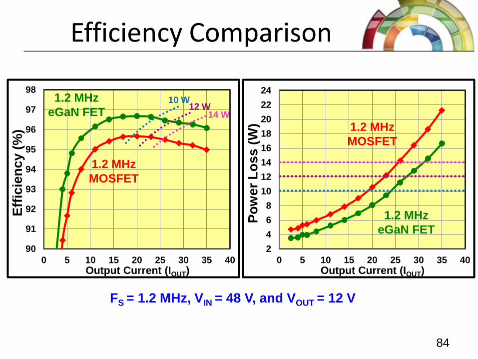
Efficiency Comparison
90
91
92
93
94
95
96
97
98
0 5 10 15 20 25 30 35 40
Effic
ienc
y (%
)
Output Current (IOUT)
1.2 MHz MOSFET
1.2 MHz eGaN FET
10 W 12 W
14 W
2 4 6 8
10 12 14 16 18 20 22 24
0 5 10 15 20 25 30 35 40 Po
wer
Los
s (W
) Output Current (IOUT)
1.2 MHz eGaN FET
1.2 MHz MOSFET
FS = 1.2 MHz, VIN = 48 V, and VOUT = 12 V
84
0
2
4
6
8
10
12
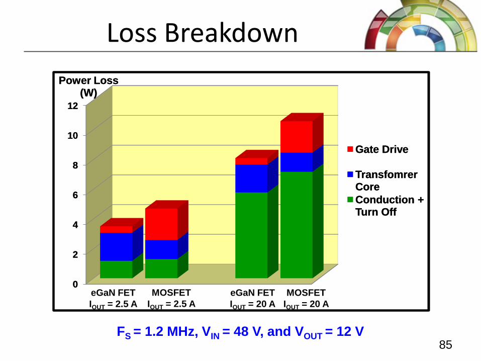
Power Loss (W)
Gate Drive
Transfomrer Core Conduction + Turn Off
0
2
4
6
8
10
12
Power Loss (W)
Gate Drive
Transfomrer Core Conduction + Turn Off
eGaN FET IOUT = 20 A
MOSFET IOUT = 20 A
eGaN FET IOUT = 2.5 A
MOSFET IOUT = 2.5 A
FS = 1.2 MHz, VIN = 48 V, and VOUT = 12 V
Loss Breakdown
85
LK2
**
*
VIN-
VIN+ VOUT+
LIN
CIN
LK1
4:1
LOUT
COUTCRES
Q1
Q2 Q4
Q3
VOUT-
Q6,Q7
Q5,Q8
2 SR
2 SR
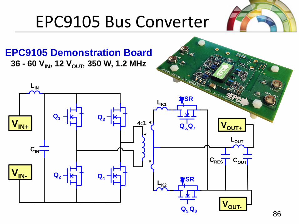
EPC9105 Demonstration Board 36 - 60 VIN, 12 VOUT, 350 W, 1.2 MHz
EPC9105 Bus Converter
86
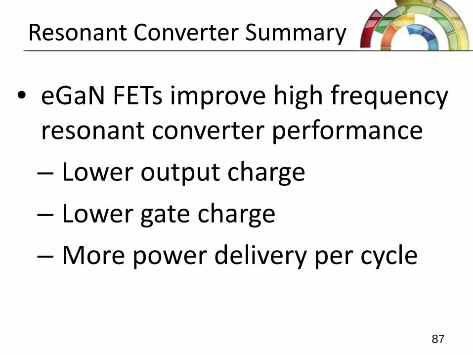
Resonant Converter Summary
• eGaN FETs improve high frequency resonant converter performance – Lower output charge – Lower gate charge – More power delivery per cycle
87 87
Summary • GaN transistors have the potential to replace
silicon power MOSFETs in power conversion applications with a low-cost and higher efficiency solution
• eGaN FETs are straightforward to use, but care must be taken due to the higher switching speeds compared with power MOSFETs
• GaN transistors enable exciting new applications such as RF Envelope Tracking
88 88


