This is information on a product in full production. November 2017 DocID025792 Rev 3 1/35 STC3117 Gas gauge IC with battery charger control for handheld applications Datasheet - production data Features Patented OptimGauge™ algorithm for accurate battery capacity calculation Robust initial open-circuit-voltage (OCV) measurement at power up Programmable low battery alarm Missing/swapped battery detection Average current internal calculation End-of-charge detection Internal temperature sensor Battery swap detection with protection against false battery insertion Low power: 40 μA in voltage-only mode, 2 μA max in standby mode 1.49 x 1.594 mm 9-bump CSP package Applications Mobile phones, multimedia players, digital cameras Portable medical equipment Description The STC3117 includes the STMicroelectronics OptimGauge™ algorithm. It provides accurate battery state-of-charge (SOC) monitoring, tracks battery parameter changes with operation conditions, temperature, and aging, and allows the application to get a battery state-of-health (SOH) indication. An alarm output signals low SOC or low voltage conditions and also indicates fault conditions like a missing or swapped battery. CSP (1.49 x 1.594 mm) www.st.com
Transcript
This is information on a product in full production.
November 2017 DocID025792 Rev 3 1/35
STC3117
Gas gauge IC with battery charger control for handheld applications
Datasheet - production data
Features
Patented OptimGauge™ algorithm for accurate battery capacity calculation
Robust initial open-circuit-voltage (OCV) measurement at power up
Programmable low battery alarm
Missing/swapped battery detection
Average current internal calculation
End-of-charge detection
Internal temperature sensor
Battery swap detection with protection against false battery insertion
Low power: 40 µA in voltage-only mode, 2 µA max in standby mode
1.49 x 1.594 mm 9-bump CSP package
Applications
Mobile phones, multimedia players, digital cameras
Portable medical equipment
Description
The STC3117 includes the STMicroelectronics OptimGauge™ algorithm. It provides accurate battery state-of-charge (SOC) monitoring, tracks battery parameter changes with operation conditions, temperature, and aging, and allows the application to get a battery state-of-health (SOH) indication.
An alarm output signals low SOC or low voltage conditions and also indicates fault conditions like a missing or swapped battery.CSP (1.49 x 1.594 mm)
1. I = input, 0 = output, OD = open drain, A = analog, D = digital, NC = not connected
Function
C3 ALM O/ODAlarm signal output, open drain, external pull-up with resistor
A2 SDA I/OD I2C serial data
B2 SCL I_D I2C serial clock
A3 GND Ground Analog and digital ground
B3 CS I_A Current sensing input
B1 BATD I/OA Battery detection input
A1 CD O/OD Battery charge inhibit (active high output)
C2 VCC Supply Power supply
C1 VIN I_A Battery voltage sensing input
Top view (balls are underneath)
GNDCD
CS
VIN ALM
SCLBATD
VCC
SDA
CSP (1.49 x 1.594 mm)
Absolute maximum ratings and operating conditions STC3117
6/35 DocID025792 Rev 3
3 Absolute maximum ratings and operating conditions
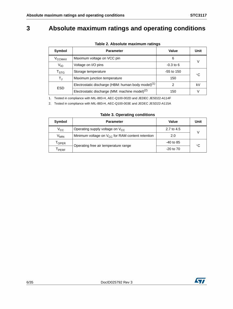
Table 2. Absolute maximum ratings
Symbol Parameter Value Unit
VCCMAX Maximum voltage on VCC pin 6V
VIO Voltage on I/O pins -0.3 to 6
TSTG Storage temperature -55 to 150C
TJ Maximum junction temperature 150
ESDElectrostatic discharge (HBM: human body model)(1)
1. Tested in compliance with MIL-883-H, AEC-Q100-002D and JEDEC JESD22-A114F
2 kV
Electrostatic discharge (MM: machine model)(2)
2. Tested in compliance with MIL-883-H, AEC-Q100-003E and JEDEC JESD22-A115A
150 V
Table 3. Operating conditions
Symbol Parameter Value Unit
VCC Operating supply voltage on VCC 2.7 to 4.5V
VMIN Minimum voltage on VCC for RAM content retention 2.0
TOPEROperating free air temperature range
-40 to 85C
TPERF -20 to 70
DocID025792 Rev 3 7/35
STC3117 Electrical characteristics
35
4 Electrical characteristics
Table 4. Electrical characteristics (2.7 V < VCC < 4.5 V, -20C to 70C)
Symbol Parameter Conditions Min Typ Max Units
Supply
ICC Operating current consumption
Average value over 4 s in voltage mode
40
µA
Average value over 4 s in mixed mode
80
ISTBY Current consumption in standbyStandby mode, inputs = 0 VBATD_PU bit = 0
2
IPDN Current consumption in power-downVCC < UVLOTH, inputs = 0 V
1
UVLOTH Undervoltage threshold (VCC decreasing) 2.5 2.6 2.7 V
UVLOHYST Undervoltage threshold hysteresis 100 mV
POR Power-on reset threshold (VCC decreasing) 2.0 V
Current sensing
Vin_gg Input voltage range -40 +40 mV
IIN Input current 500 nA
ADC_res AD converter granularity 5.88 µV
ADC_offset AD converter offset CS = 0 V -3 3 LSB
ADC_time AD conversion time 500 ms
ADC_accAD converter gain accuracy at full scale (using external sense resistor)
25 C 0.5%
Over temperature range 1
FOSC Internal time base frequency 32768 Hz
Osc_acc Internal time base accuracy
25 C, VCC = 3.6 V 2
%Over temperature and voltage ranges
2.5
Cur_res Current register LSB value 5.88 µV
Battery voltage and temperature measurement
Vin_adc Input voltage range VCC = 4.5 V 0 4.5 V
LSB LSB valueVoltage measurement 2.20 mV
Temperature measurement 1 °C
ADC_time AD conversion time 250 ms
Volt_acc Battery voltage measurement accuracy
2.7 V < Vin < 4.5 V, VCC = Vin, 25 C
-0.25 +0.25%
Over temperature range -0.5 +0.5
Temp_acc Internal temperature sensor accuracy -3 3 °C
Electrical characteristics STC3117
8/35 DocID025792 Rev 3
Digital I/O pins (SCL, SDA, ALM)
Vih Input logic high 1.2
VVil Input logic low 0.35
Vol Output logic low (SDA, ALM) Iol = 4 mA 0.4
Analog I/O pins (BATD, CD)
Vith BATD input threshold voltage 1.46 1.61 1.76V
Vihyst BATD input voltage hysteresis 0.1
Ru BATD internal pull-up resistor 1 M
Vcdoh CD output logic high Ioh = 3 mAVCC- 0.4 V
Vinmin_cd Minimum Vin voltage for CD operation 0°C to 50°C 3.6 3.75 3.9
Table 4. Electrical characteristics (2.7 V < VCC < 4.5 V, -20C to 70C) (continued)
Symbol Parameter Conditions Min Typ Max Units
DocID025792 Rev 3 9/35
STC3117 Electrical characteristics
35
Figure 3. I2C timing diagram
Table 5. I2C timing - VIO = 2.8 V, Tamb = -20 °C to 70 C (unless otherwise specified)
Symbol Parameter Min Typ Max Unit
Fscl SCL clock frequency 0
—
400 kHz
thd,sta Hold time (repeated) START condition 0.6
µs
tlow LOW period of the SCL clock 1.3
thigh HIGH period of the SCL clock 0.6
tsu,sta Setup time for repeated START condition 0.6
thd,dat Data hold time 0 0.9
tsu,dat Data setup time 100
nstr Rise time of both SDA and SCL signals
20+0.1Cb
300
tf Fall time of both SDA and SCL signals20+
0.1Cb300
tsu,sto Setup time for STOP condition 0.6
µstbuf
Bus free time between a STOP andSTART condition
1.3
Cb Capacitive load for each bus line 400 pF
Application information STC3117
10/35 DocID025792 Rev 3
5 Application information
Figure 4. Example of an application schematic
Table 6. External component list
Name Value Tolerance Comments
Rs 5 to 50 m 1 % to 5 % Current sense resistor (2% or better recommended)
C1 1 µF Supply decoupling capacitor
C2 220 nFBattery voltage input filter (optional)
R11 k
R2 Battery detection function
IO voltage
Optional filter
GND
Battery pack
Otherdetection
circuit
Rid
C1 R1
STC3117
R2
SCLSDA
ALM
CD
VCC
VIN
BATD
CS
C2
Rs
DocID025792 Rev 3 11/35
STC3117 Functional description
35
6 Functional description
6.1 Battery monitoring functions
6.1.1 Operating modes
The monitoring functions include the measurement of battery voltage, current, and temperature. A Coulomb counter is available to track the SOC when the battery is charging or discharging at a high rate. A sigma-delta A/D converter is used to measure the voltage, current, and temperature.
The STC3117 can operate in two different modes with different power consumption (see Table 7. Mode selection is made by the VMODE bit in register 0 (refer to Table 12 for register 0 definition).
In mixed mode, current is measured continuously (except for a conversion cycle every 4 s and every 16 s for measuring voltage and temperature respectively). This provides the highest accuracy from the gas gauge.
In voltage mode with no current sensing, a voltage conversion is made every 4 s and a temperature conversion every 16 s. This mode provides the lowest power consumption.
It is possible to switch between the two operating modes to get the best accuracy during active periods, and to save power during standby periods while still keeping track of the SOC information.
6.1.2 Battery voltage monitoring
Battery voltage is measured by using one conversion cycle of the A/D converter every 4 s.
The conversion cycle takes 213 = 8192 clock cycles. Using the 32768 Hz internal clock, the conversion cycle time is 250 ms.
The voltage range is 0 to 4.5 V and resolution is 2.20 mV. Accuracy of the voltage measurement is ±0.5 % over the temperature range. This allows accurate SOC information from the battery open-circuit voltage.
The result is stored in the REG_VOLTAGE register (see Table 11).
Table 7. STC3117 operating modes
VMODE Description
0 Mixed mode, Coulomb counter is active, voltage gas gauge runs in parallel
1Voltage gas gauge with power savingCoulomb counter is not used. No current sensing.
Functional description STC3117
12/35 DocID025792 Rev 3
6.1.3 Internal temperature monitoring
The chip temperature (close to the battery temperature) is measured using one conversion cycle of the A/D converter every 16 s.
The conversion cycle takes 213 = 8192 clock cycles. Using the 32768 Hz internal clock, the conversion cycle time is 250 ms. Resolution is 1° C and range is -40 to +125 °C.
The result is stored in the REG_TEMPERATURE register (see Table 11).
6.1.4 Current sensing in mixed mode
Current sensing is available only in mixed mode (VMODE=0).
The voltage drop across the sense resistor is integrated during a conversion period and is input to the 14-bit sigma-delta A/D converter.
Using the 32768 Hz internal clock, the conversion cycle time is 500 ms for a 14-bit resolution. The LSB value is 5.88 µV. The A/D converter output is in two’s complement format.
When a conversion cycle is completed, the result is added to the Coulomb counter accumulator and the number of conversions is incremented in a 16-bit counter.
The current register is updated after each conversion (that is: once per 500-ms measurement cycle). The result is stored in the REG_CURRENT register (see Table 11).
Average current register
In mixed mode, an average value of the current measurement is calculated after each current measurement with a time constant of 2 s.
The register REG_AVG_CURRENT (2 bytes) holds the average current when VMODE=0.
The LSB of REG_AVG_CURRENT is 1/4 the LSB of REG_CURRENT, that is 1.47 µV.
6.1.5 SOC change rate in voltage mode
Current sensing is not available in voltage mode (VMODE=1). Instead, an estimation of the SOC change rate is provided in the REG_AVG_CURRENT register.
The SOC change rate is updated after each SOC calculation (that is: once per 4-s measurement cycle) and is averaged with a time constant of 64 seconds. It is possible to write an initial estimation into the REG_AVG_CURRENT register to speed-up the SOC change rate settling time.
The REG_AVG_CURRENT register (2 bytes) holds the SOC change rate when VMODE=1.
The LSB of REG_AVG_CURRENT is 0.008789 C (by definition, 1 C means 100% SOC change in 1 h).
DocID025792 Rev 3 13/35
STC3117 Functional description
35
6.2 STC3117 gas gauge architecture
6.2.1 Coulomb counter
The Coulomb counter is used to track the SOC of the battery when the battery is charging or discharging at a high rate. Each current conversion result is accumulated (Coulomb counting) for the calculation of the relative SOC value based on the configuration register.
The system controller can control the Coulomb counter and set and read the SOC register through the I2C control registers.
Figure 5. Coulomb counter block diagram
The REG_CC_CNF value depends on battery capacity and the current sense resistor. It scales the charge integrated by the sigma delta converter into a percentage value of the battery capacity. The default value is 395 (corresponding to a 10-m sense resistor and 1957-mAh battery capacity).
The Coulomb counter is inactive if the VMODE bit is set, this is the default state at power-on-reset (POR) or reset (VMODE bit = 1).
Writing a value to the register REG_SOC (mixed mode SOC) forces the Coulomb counter gas gauge algorithm to restart from this new SOC value.
REG_CC_CNF register is a 16-bit integer value CC_CNF that is calculated as shown in Equation 1:
No current sensing is needed for the voltage gas gauge. An internal algorithm precisely simulates the dynamic behavior of the battery and provides an estimation of the OCV. The battery SOC is related to the OCV by means of a high-precision reference OCV curve built into the STC3117.
Any change in battery voltage causes the algorithm to track both the OCV and SOC values, taking into account the non-linear characteristics and time constants related to the chemical nature of the Li-Ion and Li-Po batteries.
A single parameter fits the algorithm to a specific battery. The default value provides good results for most battery chemistries used in hand-held applications.
Figure 6. Voltage gas gauge block diagram
Voltage gas gauge algorithm registers
The REG_VM_CNF configuration register is used to configure the parameter used by the algorithm based on battery characteristic. The default value is 321 (corresponding to 160 m internal battery impedance and 1957 mAh Cnom battery capacity).
The REG_OCV register holds the estimated OCV value corresponding to the present battery state.
The REG_OCVTAB and REG_SOCTAB registers define the OCV curve for a given battery type; the default power-up values can be updated at software initialization.
The REG_VM_CNF register is a 12-bit integer value and is calculated from the averaged internal resistance and nominal capacity of the battery as shown in Equation 2:
Equation 2
Ri is in mand Cnom is in mAh.
Example: Ri = 250 m, Cnom =1500 mAh, VM_CNF= 384
Voltage mode
algorithm To SOCmanagement
(VM)
ReferenceOCVcurve
AD converter
VIN
registerREG_VOLTAGE
registerREG_VM_CNF
registerREG_OCV
registerREG_OCVTAB
registerREG_SOCTAB
VM_CNF Ri Cnom 977.78=
DocID025792 Rev 3 15/35
STC3117 Functional description
35
6.2.3 Mixed mode gas gauge system
The STC3117 implements a mixed mode gas gauge (OptimGaugeTM 1) that uses both the Coulomb counter (CC) and the voltage mode (VM) algorithm to track the battery SOC in all application conditions and automatically provide the optimum SOC information. The VM algorithm cancels any long-term errors and prevents the SOC drift problem that is commonly found in CC-only solutions.
The STC3117 automatically selects the best method based on the relaxation timer (see Section 6.4: Current monitoring) as follows: when a low-power application state is detected by the relaxation timer, the SOC reported by the STC3117 is the VM SOC, otherwise the CC SOC is reported. The STC3117 manages the transitions between the VM and CC modes without discontinuity by adjusting the VM and the CC SOC to ensure smooth SOC variations without jumps in any application conditions.
The current mixed mode state is indicated by the GG_VM bit in the REG_CTRL register: GG_VM=1 means the reported SOC is the VM SOC, otherwise the SOC is the CC SOC.
Note: When the application enters standby mode, the STC3117 can be put into power-saving mode by setting the VMODE bit to 1 in the REG_MODE register. Only the VM gas gauge stays active, the CC is stopped, and the power consumption is reduced.
Figure 7. Mixed mode gas gauge block diagram
Adjustment registers
The registers REG_CC_ADJ and REG_VM_ADJ are signed 16-bit registers. They accumulate the adjustment quantities made to the SOC values by the embedded mixed mode algorithm:
REG_CC_ADJ = REG_SOC – (unadjusted CC SOC)
REG_VM_ADJ = REG_SOC – (unadjusted VM SOC)
These registers can be used by the system application to implement more sophisticated algorithms for improved performance and accuracy.
Writing to the REG_SOC or REG_OCV initializes the two VM and CC algorithms to the corresponding SOC value and clears REG_VM_ADJ and REG_CC_ADJ. It is possible to write to the REG_SOC, REG_OCV, REG_VM_CNF and REG_CC_CNF registers when the STC3117 is running without disturbing SOC management.
Note: When writing to the REG_SOC or REG_OCV registers, the resulting SOC value is rounded to the nearest 1/64 % value (the least three bits of REG_SOC are zero).
Voltage mode(VM)
REG_SOCregister
Alarmmanagement
Parametertracking
Coulomb counter
REG_VM_ADJregister
REG_CC_ADJregister
(CC)
SOCmanagement
gas gauge
Functional description STC3117
16/35 DocID025792 Rev 3
6.3 Alarm output
The ALM pin provides an alarm signal in case of low battery or fault condition. The output is an open drain, and an external pull-up resistor is needed in the application. Writing the IO0DATA bit to 0 forces the ALM output low; writing the IO0DATA bit to 1 lets the ALM output reflect the battery condition. Reading the IO0DATA bit gives the state of the ALM pin.
When the IO0DATA bit is 1, the ALM pin is driven low if any of the following conditions are met:
the battery SOC estimation from the mixed algorithm is less than the programmed threshold (if the alarm function is enabled by the ALM_ENA bit)
the battery voltage is less than the programmed low voltage level (if the ALM_ENA bit is set)
the BATFAIL bit is set (if the ALM_ENA bit is set)
Low-voltage or low-SOC alarms
When a low-voltage or low-SOC condition is triggered, the STC3117 drives the ALM pin low and sets the ALM_VOLT or ALM_SOC bit in REG_CTRL.
The ALM pin remains low (even if the conditions disappear) until the software writes the ALM_VOLT and ALM_SOC bits to 0 to clear the interrupt.
Clearing the ALM_VOLT or ALM_SOC while the corresponding low-voltage or low-SOC condition is still true does not generate another interrupt; this condition must disappear first and must be detected again before another interrupt (ALM pin driven low) is generated for this alarm. The other alarm condition, if not yet triggered, can still generate an interrupt.
Usually, the low-SOC alarm occurs first to warn the application of a low battery condition, then if no action is taken and the battery discharges further, the low-voltage alarm signals a nearly-empty battery condition.
At power-up, or when the STC3117 is reset, the SOC and voltage alarms are enabled (ALM_ENA bit = 1). The ALM pin is in high-impedance directly after a POR and is driven low if the SOC and/or the voltage is below the default thresholds (1% SOC, 3.00 V), after the first OCV measurement and SOC estimation.
The REG_SOC_ALM register holds the relative SOC alarm level in 0.5 % units (0 to 100 %). Default value is 2 (i.e. 1 % SOC).
The REG_ALARM_VOLTAGE holds the low voltage threshold and can be programmed over the full scale voltage range with 17.60 (2.20*8) mV steps. Default value is 170 (i.e. 3.00 V).
BATFAIL alarm
The BATFAIL bit in REG_CTRL reflects the battery swap event: BATFAIL bit is set when the BATD signal rises above the BATD threshold (1.61 V typ) for more than 0.5 s. and is reset by writing 0 to the BATFAIL bit if the BATD signal is below the BATD threshold (if BATD is still above 1.61 V, then BATFAIL bit can not be cleared).
The STC3117 drives the ALM pin low when the BATFAIL bit is set and releases the ALM pin when the BATFAIL bit is cleared.
DocID025792 Rev 3 17/35
STC3117 Functional description
35
6.4 Current monitoring
The battery average current is monitored and is used in conjunction with a timer to implement a battery relaxation timer.
Battery relaxation timer
The battery relaxation timer is used to detect a light-load, low-power condition.
The REG_CMONIT_COUNT register is an 8-bit, read-only counter that is incremented every 4 s when the average current is inside a window defined by positive and negative thresholds set by the REG_CURRENT_THRES register, and decremented every 500 ms when the current is outside the thresholds.
When the counter reaches its maximum value set by the REG_CMONIT_MAX register, a low-power condition is reported to the mixed mode algorithm causing VM mode to be used. When the counter reaches its minimum value (0), a high-power condition is reported and CC mode is used.
The REG_CMONIT_MAX register sets the maximum value of the counter. With the default value (120 dec), the counter provides an 8-minute delay when switching from CC to VM mode and a 1-minute delay when switching from VM to CC mode.
The REG_CURRENT_THRES register is an 8-bit R/W register set by the gas gauge firmware from the I2C. It holds the threshold amplitude in bits 0 to 6 (unsigned value applicable for both positive and negative thresholds). Bit 7 of REG_CURRENT_THRES is reserved and must be set to zero for operation of the current monitoring counter as a relaxation timer. The LSB value of the REG_CURRENT_THRES is 47.04 µV and provides a range of 0 to 6 mV.
It is possible to set the counter to zero or the maximum value using the FORCE_CC and FORCE_VM bits in the REG_MODE register. These bits are self-clearing.
Functional description STC3117
18/35 DocID025792 Rev 3
6.5 Power-up and battery swap detection
When the STC3117 is powered up at first battery insertion (power-on reset) or after a soft reset condition (PORDET bit set by host), an automatic battery voltage, current and temperature measurement cycle is made immediately after startup and debounce delay.
This feature enables the system controller to get the SOC of a newly inserted battery based on the OCV.
The CD pin controls the battery charger to inhibit the charge during the initial OCV measurement. The CD output is validated during the power-up/restart sequence but is actually driven high only if the battery is present (BATD < 1.61V) and the battery voltage is higher than a threshold (Vin > Vinmin_cd) at the beginning of the restart sequence.
The CD pin can be driven high under software control by using the bit FORCE_CD in the REG_MODE register.
The BATD pin senses the presence of the battery independently of the battery voltage.
Figure 8. BATD and CD internal architecture overview
The BATD pin is an analog I/O. The input detection threshold is typically 1.61 V.
The CD pin is an output connected to the VCC level when active. Otherwise, it is high impedance.
The BATD pin can be connected to the NTC sensor or to the identification resistor of the battery pack. By default, the STC3117 provides an internal pull-up resistor for the detection of battery removal. The internal resistor can be disabled by clearing the bit BATD_PU in the REG_MODE register. When disabled, an external pull-up resistor or another device has to pull the BATD pin high.
CD
BATD
VCC CD_drive
1.61 V+-
Vinmin_cd level
Vin+-
&
DocID025792 Rev 3 19/35
STC3117 Functional description
35
Figure 9. Timing diagram details of the power-up and restart sequence
Battery swap detection
A battery swap can be detected in two ways:
the battery voltage drops below the undervoltage lockout (UVLO) for more than tdel
the BATD signal rises above the BATD threshold (1.61 V typ) for more than tdel
The tdel delay is 0.5 s.
Using the 0.5 s filter provides robust battery swap detection and prevents false battery swap detection if short contact bouncing occurs at the battery terminals due to mechanical vibrations or shocks. This also prevents false detections in case of short battery voltage drops and protects the application against high surge currents at low temperatures.
Following a battery swap detection and after the battery voltage goes back above UVLO and the BATD level returns to low level, the STC3117 is on hold with new voltage and current measurements in the corresponding registers. The system has to restart the STC3117 by doing a device soft reset i.e. by setting the PORDET bit to 1 in the REG_CTRL register and restoring the parameters (if needed). To recover the event, either use the measured voltage and current to define a new OCV voltage, or restore a previous SOC state.
The occurrence of the battery swap event is indicated by the BATFAIL and UVLOD bits in the REG_CTRL register.
VCC
UVLO
Internal 1mAsink current
Voltage measurement
delay
CD pin(low means HiZ)
OCV meas.
Application can start, charge is enabled
Currentmeasurement
Temperaturemeasurement
125ms
Conversion counter
X 0 1 2 3
Vinmin_cd
Ibatmeas.
(arbitrary Vccwaveforms only to illustrate the function)
“Dead” battery
“Good” battery
GAMS1601141520CB
“Good” battery “Dead” battery
375 ms
125ms
125ms
250ms
100ms
Functional description STC3117
20/35 DocID025792 Rev 3
Figure 10. Restart in case of battery swap
VCC UVLO
BATD
Short UVLO event < 0.5sNo restart,
No operation interruptionBATFAIL=0UVLOD=0
<0.5s
Short battery disconnection event < 0.5sNo restart,
No operation interruptionBATFAIL=0UVLOD=0
<0.5s
POR
Battery removal, fast Vcc drop,
Restart at powerup
PORDET=1BATFAIL=0UVLOD=0
1.61V
DocID025792 Rev 3 21/35
STC3117 I2C interface
35
7 I2C interface
7.1 Read and write operations
The I2C interface is used to control and read the current accumulator and registers. It is compatible with the Philips I2C Bus® (version 2.1). It is a slave serial interface with a serial data line (SDA) and a serial clock line (SCL).
SCL: input clock used to shift data
SDA: input/output bidirectional data transfers
A filter rejects the potential spikes on the bus data line to preserve data integrity.
The bidirectional data line supports transfers up to 400 Kbit/s (fast mode). The data are shifted to and from the chip on the SDA line, MSB first.
The first bit must be high (START) followed by the 7-bit device address and the read/write control bit. The default device address value is 1110 000. The STC3117 then sends an acknowledge at the end of an 8-bit long sequence. The next eight bits correspond to the register address followed by another acknowledge.
The data field is the last 8-bit long sequence sent, followed by a final acknowledge.
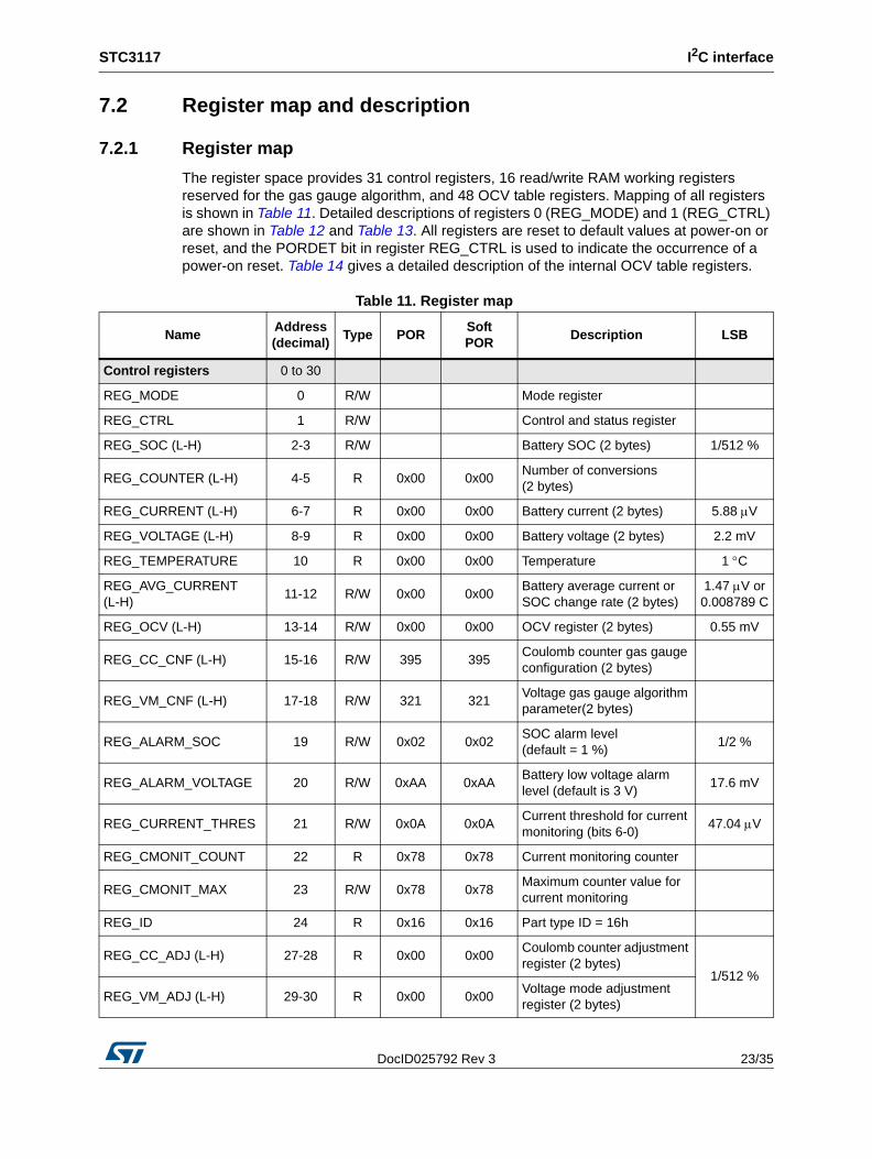
The register space provides 31 control registers, 16 read/write RAM working registers reserved for the gas gauge algorithm, and 48 OCV table registers. Mapping of all registers is shown in Table 11. Detailed descriptions of registers 0 (REG_MODE) and 1 (REG_CTRL) are shown in Table 12 and Table 13. All registers are reset to default values at power-on or reset, and the PORDET bit in register REG_CTRL is used to indicate the occurrence of a power-on reset. Table 14 gives a detailed description of the internal OCV table registers.
Values held in consecutive registers (such as the SOC value in the REG_SOC register pair) are stored with low bits in the low-address register (L) and high bits in the high-address register (H). The registers must be read with a single I2C access to ensure data integrity. It is possible to read multiple values in one I2C access. All values must be consistent.
The SOC data are coded in binary format and the LSB of the low byte is 1/512 %. The battery current is coded in 2’s complement format and the LSB value is 5.88 µV. The battery voltage is coded in 2’s complement format and the LSB value is 2.20 mV. The temperature is coded in 2’s complement format and the LSB value is 1°C.
RAM registers 32 to 47
REG_RAM0 32 R/W 0x00 0x00Working register 0 for gas gauge
... ... ...
REG_RAM15 47 R/W 0x00 0x00Working register 15 for gas gauge
OCV table registers 48 to 95
REG_OCVTAB0 (L-H) to REG_OCVTAB15 (L-H)
48-49 to 78-79
R/WSee
table 14See
table 14OCV points, 2 bytes per point (32 registers)
0.55 mV
REG_SOCTAB0 to REG_SOCTAB15
80 to 95 R/WSee
table 14See
table 14SOC points, 1 byte per point (16 registers)
1/2 %
Table 11. Register map (continued)
NameAddress (decimal)
Type PORSoftPOR
Description LSB
DocID025792 Rev 3 25/35
STC3117 I2C interface
35
7.2.3 REG_MODE and REG_CTRL register description
Table 12. REG_MODE - address 0
Name Position Type Def. Description
VMODE 0 R/W 10: Mixed mode (Coulomb counter active)1: Power saving voltage mode
0: Standby mode. Accumulator and counter registers are frozen, gas gauge and battery monitor functions are in standby.1: Operating mode
FORCE_CC 5 R/W 0
Forces the relaxation timer to switch to the Coulomb counter (CC) state.Write 1, self clear to 0Relaxation counter = 0
FORCE_VM 6 R/W 0
Forces the relaxation timer to switch to voltage mode (VM) state.Write 1, self clear to 0Relaxation counter = Relax_max
7 Unused
I2C interface STC3117
26/35 DocID025792 Rev 3
Table 13. REG_CTRL - address 1
Name Position Type Def. Description
IO0DATA 0
R XALM pin status0 = ALM input is low1 = ALM input is high
W 1ALM pin output drive0 = ALM is forced low1 = ALM is driven by the alarm conditions
GG_RST 1 W 00: no effect1: resets the conversion counterGG_RST is a self-clearing bit.
GG_VM 2 R 0Voltage mode active0 = REG_SOC from Coulomb counter mode1 = REG_SOC from Voltage mode
BATFAIL 3 R/W 0Battery removal (BATD high). Write 0 to clear (effective only if BATD low)(Write 1 is ignored)
PORDET 4
R 1Power on reset (POR) detection bit0 = no POR event occurred1 = POR event occurred
W 0
Soft reset0 = release the soft-reset and clear the POR detection bit,1 = assert the soft-reset and set the POR detection bit. This bit is self clearing.
ALM_SOC 5 R/W 0Set with a low-SOC condition. Cleared by writing 0.
ALM_VOLT 6 R/W 0Set with a low-voltage condition. Cleared by writing 0.
UVLOD 7 R/W 0UVLO event detection.Cleared by writing 0.
DocID025792 Rev 3 27/35
STC3117 I2C interface
35
7.2.4 OCV table register description
Table 14. Default OCV table and OCV table registers
Table entry
Default SOC Default OCV
SOC register OCV register%
Hex code
mV Hex code
0 0 00 3300 1770 REG_SOCTAB0 REG_OCVTAB0
1 3 06 3541 1926 REG_SOCTAB1 REG_OCVTAB1
2 6 0C 3618 19B2 REG_SOCTAB2 REG_OCVTAB2
3 10 14 3658 19FB REG_SOCTAB3 REG_OCVTAB3
4 15 1E 3695 1A3E REG_SOCTAB4 REG_OCVTAB4
5 20 28 3721 1A6D REG_SOCTAB5 REG_OCVTAB5
6 25 32 3747 1A9D REG_SOCTAB6 REG_OCVTAB6
7 30 3C 3761 1AB6 REG_SOCTAB7 REG_OCVTAB7
8 40 50 3778 1AD5 REG_SOCTAB8 REG_OCVTAB8
9 50 64 3802 1B01 REG_SOCTAB9 REG_OCVTAB9
10 60 78 3863 1B70 REG_SOCTAB10 REG_OCVTAB10
11 65 82 3899 1BB1 REG_SOCTAB11 REG_OCVTAB11
12 70 8C 3929 1BE8 REG_SOCTAB12 REG_OCVTAB12
13 80 A0 3991 1C58 REG_SOCTAB13 REG_OCVTAB13
14 90 B4 4076 1CF3 REG_SOCTAB14 REG_OCVTAB14
15 100 C8 4176 1DA9 REG_SOCTAB15 REG_OCVTAB15
Package information STC3117
28/35 DocID025792 Rev 3
8 Package information
In order to meet environmental requirements, ST offers these devices in different grades of ECOPACK® packages, depending on their level of environmental compliance. ECOPACK® specifications, grade definitions and product status are available at: www.st.com. ECOPACK® is an ST trademark.
8.1 Flip Chip CSP 1.49 x 1.594 x 0.4 mm (N5) with coating ball printing package information
Figure 13. Flip Chip CSP 1.49 x 1.594 x 0.4 mm (N5) package mechanical drawing
1. The terminal A1 on the bump side is identified by a distinguishing feature - for instance, by a circular “clear area” typically 0.1 mm in diameter and/or a missing bump.
2. The terminal A1, on the back side, is identified by a distinguishing feature - for instance, by a circular “clear area” typically 0.2 mm in diameter depending on the die size.
D1fD
e
C
B
A
SE
fE1
fE2
e
E1
321Bottom view
Top view
E
D
ccc C
A
A1
A2
C
Øb
$
GAMS1701141057CB
A1 (see note 1 and 2)
Package information STC3117
30/35 DocID025792 Rev 3
Table 15. Flip Chip CSP 1.49 x 1.594 x 0.4 mm (N5) package mechanical data
Ref.
Dimensions
Millimeters Inches
Min. Typ. Max. Min. Typ. Max.
A 0.545 0.60 0.655 0.021 0.024 0.026
A1 0.17 0.20 0.23 0.007 0.008 0.009
A2 0.38 0.4 0.42 0.015 0.016 0.017
b 0.23 0.26 0.29 0.009 0.010 0.011
D 1.43 1.46 1.49 0.056 0.057 0.059
D1 0.8 0.031
E 1.534 1.564 1.594 0.060 0.062 0.063
E1 0.8 0.031
e 0.4 0.016
SE 0.015 0.001
fD 0.32 0.33 0.34 0.013 0.013 0.013
fE1 0.357 0.367 0.377 0.014 0.014 0.015
fE2 0.387 0.397 0.407 0.015 0.016 0.016
$ 0.05 0.002
ccc 0.05 0.002
DocID025792 Rev 3 31/35
STC3117 Package information
35
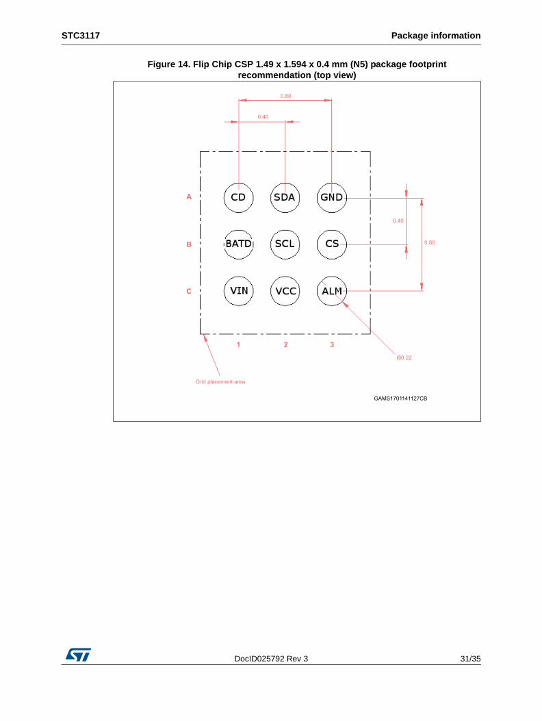
Figure 14. Flip Chip CSP 1.49 x 1.594 x 0.4 mm (N5) package footprint recommendation (top view)
C
B
A
321
0.80
Grid placement area
0.80
0.40
0.40
Ø0.22
GAMS1701141127CB
Package information STC3117
32/35 DocID025792 Rev 3
Figure 15. Flip Chip CSP 1.49 x 1.594 x0.4 mm (N5) package reflow profile recommendation
GAMS1701141140CB
DocID025792 Rev 3 33/35
STC3117 Ordering information
35
9 Ordering information
Table 16. Order code
Order code Temperature range Package Packing Marking
STC3117IJT -40°C to +85°C CSP 9-bump Tape and reel VWV
Revision history STC3117
34/35 DocID025792 Rev 3
10 Revision history
Table 17. Document revision history
Date Revision Changes
23-Jul-2014 1 Initial release
19-Jan-2015 2
Updated "low power" value in Features
Updated Section 6.1.4: Current sensing in mixed mode
Added Section 6.1.5: SOC change rate in voltage mode
Updated Figure 5: Coulomb counter block diagram
Updated example of Equation 2
Re-wrote Section 6.2.3: Mixed mode gas gauge system
Re-wrote Section 6.4: Current monitoring
Updated Section 6.5: Power-up and battery swap detection.
Updated Table 11: Register map
Updated Table 12: REG_MODE - address 0
Updated Table 13: REG_CTRL - address 1
10-Nov-2017 3Updated tsu,sta symbol in Table 5: I2C timing - VIO = 2.8 V, Tamb = -20 °C to 70 C (unless otherwise specified).
DocID025792 Rev 3 35/35
STC3117
35
IMPORTANT NOTICE – PLEASE READ CAREFULLY
STMicroelectronics NV and its subsidiaries (“ST”) reserve the right to make changes, corrections, enhancements, modifications, and improvements to ST products and/or to this document at any time without notice. Purchasers should obtain the latest relevant information on ST products before placing orders. ST products are sold pursuant to ST’s terms and conditions of sale in place at the time of order acknowledgement.
Purchasers are solely responsible for the choice, selection, and use of ST products and ST assumes no liability for application assistance or the design of Purchasers’ products.
No license, express or implied, to any intellectual property right is granted by ST herein.
Resale of ST products with provisions different from the information set forth herein shall void any warranty granted by ST for such product.
ST and the ST logo are trademarks of ST. All other product or service names are the property of their respective owners.
Information in this document supersedes and replaces information previously supplied in any prior versions of this document.