23
www.madeeasy.in Write us at [email protected] | Phone: 011-45124612, 9958995830 GATE-2014 Detailed Solutions Electronics Engg. of Morning Session 15th Feb, 2014 www.myengg.com
| Date post: | 03-Jun-2018 |
| Category: |
Documents |
| Upload: | lokesh-kumar |
| View: | 218 times |
| Download: | 0 times |

8/12/2019 GATE 2014 Electronics Engineering Keys & Solution on 15th (Morning Session)
http://slidepdf.com/reader/full/gate-2014-electronics-engineering-keys-solution-on-15th-morning-session 1/23
www.madeeasy.in
Write us at [email protected] | Phone: 011-45124612, 9958995830
GATE-2014
Detailed Solutions
Electronics Engg.of
Morning Session
15th Feb, 2014
www.myengg.com

8/12/2019 GATE 2014 Electronics Engineering Keys & Solution on 15th (Morning Session)
http://slidepdf.com/reader/full/gate-2014-electronics-engineering-keys-solution-on-15th-morning-session 2/23
Corporate Office: 44-A/1, Kalu Sarai, New Delhi-16 | Email : [email protected] | Visit: www.madeeasy.in
GATE-2014 Exam Solutions (15 Feb)
Electronics Engineering (Morning Session)
1 2 3 4 5 6 7 8 9 0
1 2 3 4 5 6 7 8 9 0
1 2 3 4 5 6 7 8 9 0
1 2 3 4 5 6 7 8 9 0
1 2 3 4 5 6 7 8 9 0
1 2 3 4 5 6 7 8 9 0
1 2 3 4 5 6 7 8 9 0
1 2 3 4 5 6 7 8 9 0
1 2 3 4 5 6 7 8 9 0
1 2 3 4 5 6 7 8 9 0
1 2 3 4 5 6 7 8 9 0
1 2 3 4 5 6 7 8 9 0
1 2 3 4 5 6 7 8 9 0
Page
1
Section - I (Technical)
Q.1 In the voltage regulator shown in figure op-amp is ideal. The BJT has VBE
=0.7V
and β = 100 and Zener voltage Vz is 4.7 V for a regulated output of 9 V the value
of R in Ω is
+
–
V = 4.7 Vz
1 kΩ
V = 12 Vi V = 9 Vo
1 K = R1
R = R2
Solution: (1093.0232)
Given circuit is a op-amp series regulator
Vo is given by
Vo = 1
z
2
R1 V
R
+
9 V =2
1k1 4.7
R
Ω+
∴ R2 = 1093.0232 Ω
Q.2 A depletion type N-channel MOS is biased in its linear region to use as a voltage
controlled resistor. Assume Vth = 0.5 V, VGS = 20 V, VDS = 5 V, =W
100,L
COX = 10 –8 F/m2, µn = 800 cm2/V-s. Find the resistance of voltage control resistor
in (Ω).
Solution: (641025.641)
Voltage controlled resistor rDS is given by
rDS = − n OX GS t
1
W(µ C ) (V V )
L
rDS = − −× × × × −4 8
1
800 10 10 100 (20 0.5)
rDS = 641.02 kΩ
www.myengg.com

8/12/2019 GATE 2014 Electronics Engineering Keys & Solution on 15th (Morning Session)
http://slidepdf.com/reader/full/gate-2014-electronics-engineering-keys-solution-on-15th-morning-session 3/23
Corporate Office: 44-A/1, Kalu Sarai, New Delhi-16 | Email : [email protected] | Visit: www.madeeasy.in
GATE-2014 Exam Solutions (15 Feb)
Electronics Engineering (Morning Session)
1 2 3 4 5 6 7 8 9 0
1 2 3 4 5 6 7 8 9 0
1 2 3 4 5 6 7 8 9 0
1 2 3 4 5 6 7 8 9 0
1 2 3 4 5 6 7 8 9 0
1 2 3 4 5 6 7 8 9 0
1 2 3 4 5 6 7 8 9 0
1 2 3 4 5 6 7 8 9 0
1 2 3 4 5 6 7 8 9 0
1 2 3 4 5 6 7 8 9 0
1 2 3 4 5 6 7 8 9 0
1 2 3 4 5 6 7 8 9 0
1 2 3 4 5 6 7 8 9 0
Page
2
Q.3 Capacity of binary symmetric channel with cross-over probability 0.5 ____.
Solution: (0)
Channel capacity of BSC is
C = Plog2P + (1 – P) log2(1 – P) + 1
C = 0.5log20.5 + 0.5log20.5 + 1
C = 0
It is the case of channel with independent input and output, hence C = 0.
Q.4 In BJT transistor VBE = 0.7 V and VT = 25 mV and reverse saturation current is
10 –13 A. Find the transconductance in mA . V
Solution: (5785.0282)
We know that
gm = c
T
I
V
where Ic =
BE
T
V
VsI e
So, Ic =
0.713 0.02510 e− ×
Ic = 144.6257 mA
Hence, gm =144 mA
5785.02820.025 V
=
Q.5 Find the RMS value of the given pulse
0
1
T/2 T t3T/2
⋅⋅⋅
www.myengg.com

8/12/2019 GATE 2014 Electronics Engineering Keys & Solution on 15th (Morning Session)
http://slidepdf.com/reader/full/gate-2014-electronics-engineering-keys-solution-on-15th-morning-session 4/23
Corporate Office: 44-A/1, Kalu Sarai, New Delhi-16 | Email : [email protected] | Visit: www.madeeasy.in
GATE-2014 Exam Solutions (15 Feb)
Electronics Engineering (Morning Session)
1 2 3 4 5 6 7 8 9 0
1 2 3 4 5 6 7 8 9 0
1 2 3 4 5 6 7 8 9 0
1 2 3 4 5 6 7 8 9 0
1 2 3 4 5 6 7 8 9 0
1 2 3 4 5 6 7 8 9 0
1 2 3 4 5 6 7 8 9 0
1 2 3 4 5 6 7 8 9 0
1 2 3 4 5 6 7 8 9 0
1 2 3 4 5 6 7 8 9 0
1 2 3 4 5 6 7 8 9 0
1 2 3 4 5 6 7 8 9 0
1 2 3 4 5 6 7 8 9 0
Page
3
Solution: (0.4082)
RMS value = ∫ T
2
0
1 f (t)dtT
where T is time period
= + ∫ ∫
2T/ 2 T2
0 T /2
1 2t dt (0) dt
T T
= ∫ T/2
2
20
1 4t dt
T T
So, RMS value =1
or 0.4086
Q.6 Let x(n) = − − − −
n n1 1
u(n) u( n 1)9 3
ROC of z-transform is
(a) <1
Z9
(b) <1
Z3
(c) > >1 1Z3 9
(d) does not exist
Solution: (c)
x(n) =
∴ > ∴ <
− − − −
n n
Righ sided signal Left sided signal
1 1ROC ROCisZ Z
9 3
1 1u(n) u( n 1)
9 3
Hence ROC is > >1 1
Z3 9
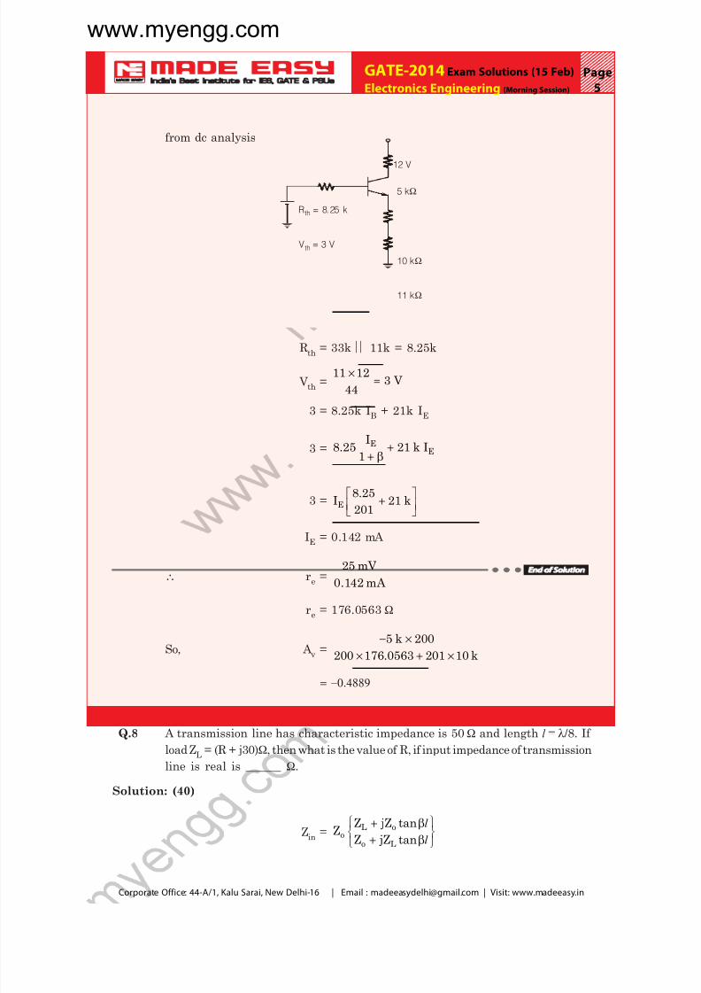
Q.7 The amplifier shown in figure. The BJT parameters are, VBE = 0.7 V, β = 200 V,
VT = 250 mV. Find the gain =o
i
V _______.
V
www.myengg.com

8/12/2019 GATE 2014 Electronics Engineering Keys & Solution on 15th (Morning Session)
http://slidepdf.com/reader/full/gate-2014-electronics-engineering-keys-solution-on-15th-morning-session 5/23
Corporate Office: 44-A/1, Kalu Sarai, New Delhi-16 | Email : [email protected] | Visit: www.madeeasy.in
GATE-2014 Exam Solutions (15 Feb)
Electronics Engineering (Morning Session)
1 2 3 4 5 6 7 8 9 0
1 2 3 4 5 6 7 8 9 0
1 2 3 4 5 6 7 8 9 0
1 2 3 4 5 6 7 8 9 0
1 2 3 4 5 6 7 8 9 0
1 2 3 4 5 6 7 8 9 0
1 2 3 4 5 6 7 8 9 0
1 2 3 4 5 6 7 8 9 0
1 2 3 4 5 6 7 8 9 0
1 2 3 4 5 6 7 8 9 0
1 2 3 4 5 6 7 8 9 0
1 2 3 4 5 6 7 8 9 0
1 2 3 4 5 6 7 8 9 0
Page
4
1 µF
Vi
R1 RC = 5 kΩ
R2 11 kΩ
10 kΩRs
Re 11 kΩ
33 kΩ
1 mF
V = +12 Vcc
Solution: (–0.4889)
RB
βre
ib
+
–
Vi
= R R1 2
βib
R = 10 ks Ω
R = 5 kC Ω
+
–
V0
Vi = βibre + (ib + βib) Rs
Vi = βibre + ib(1 + β) Rs
Vi = ib[βre + (1 + β) Rs] ...(i)
V0 = –Rcβib ...(ii)
∴0
i
V
V=
c b
b e s
R i
i [ r (1 )R ]
− × β ×β + + β
A V =c
e s
R
r (1 )R
− × ββ + + β ...(iii)
where re is given by
re =T
E
V
I
www.myengg.com
8/12/2019 GATE 2014 Electronics Engineering Keys & Solution on 15th (Morning Session)
http://slidepdf.com/reader/full/gate-2014-electronics-engineering-keys-solution-on-15th-morning-session 6/23
Corporate Office: 44-A/1, Kalu Sarai, New Delhi-16 | Email : [email protected] | Visit: www.madeeasy.in
GATE-2014 Exam Solutions (15 Feb)
Electronics Engineering (Morning Session)
1 2 3 4 5 6 7 8 9 0
1 2 3 4 5 6 7 8 9 0
1 2 3 4 5 6 7 8 9 0
1 2 3 4 5 6 7 8 9 0
1 2 3 4 5 6 7 8 9 0
1 2 3 4 5 6 7 8 9 0
1 2 3 4 5 6 7 8 9 0
1 2 3 4 5 6 7 8 9 0
1 2 3 4 5 6 7 8 9 0
1 2 3 4 5 6 7 8 9 0
1 2 3 4 5 6 7 8 9 0
1 2 3 4 5 6 7 8 9 0
1 2 3 4 5 6 7 8 9 0
Page
5
from dc analysis
V = 3 Vth
R = 8.25 kth
10 kΩ
11 kΩ
5 kΩ
12 V
Rth = 33k 11k = 8.25k
Vth =11 12
3 V44
×=
3 = 8.25k IB + 21k IE
3 =E
E
I8.25 21 k I
1+
+ β
3 = E
8.25I 21 k
201
+
IE = 0.142 mA
∴ re =25 mV
0.142 mA
re = 176.0563 Ω
So, A v =5 k 200
200 176.0563 201 10 k
− ×× + ×
= –0.4889
Q.8 A transmission line has characteristic impedance is 50 Ω and length l = λ/8. If
load ZL = (R + j30)Ω, then what is the value of R, if input impedance of transmission
line is real is ______ Ω.
Solution: (40)
Zin = + β + β
l
l
L oo
o L
Z jZ tanZ
Z jZ tan
www.myengg.com

8/12/2019 GATE 2014 Electronics Engineering Keys & Solution on 15th (Morning Session)
http://slidepdf.com/reader/full/gate-2014-electronics-engineering-keys-solution-on-15th-morning-session 7/23
Corporate Office: 44-A/1, Kalu Sarai, New Delhi-16 | Email : [email protected] | Visit: www.madeeasy.in
GATE-2014 Exam Solutions (15 Feb)
Electronics Engineering (Morning Session)
1 2 3 4 5 6 7 8 9 0
1 2 3 4 5 6 7 8 9 0
1 2 3 4 5 6 7 8 9 0
1 2 3 4 5 6 7 8 9 0
1 2 3 4 5 6 7 8 9 0
1 2 3 4 5 6 7 8 9 0
1 2 3 4 5 6 7 8 9 0
1 2 3 4 5 6 7 8 9 0
1 2 3 4 5 6 7 8 9 0
1 2 3 4 5 6 7 8 9 0
1 2 3 4 5 6 7 8 9 0
1 2 3 4 5 6 7 8 9 0
1 2 3 4 5 6 7 8 9 0
Page
6
Here β =π λ
=λ
l 2
and8
∴ tan βl =π
=tan 14
Thus, Zin = + + +
= + + −
L oo
o L
Z jZ R j30 j50Z 50
Z jZ 50 jR 30
=++
50(R j80)
(20 jR)
⇒ = +
+50(R j80)
(20 jR)
For Zin to be real
Zin = + − + −
=+ − +2
50(R j80) (20 jR) 50(R j80) (20 jR)
(20 jR) (20 jR) (R 400)
= +
+50(R j80)
(20 jR)
For Zin to be real
Zi = + − + −
=
+ − +2
50(R j80) (20 jR) 50(R j80) (20 jR)
(20 jR) (20 jR) (R 400)
⇒ –jR2 + j1600 = 0
or R = = Ω1600 40
Q.9 Which of the following equation is correct?
(a) [ ]> 22E[x ] E(x) (b) [ ]≥ 22E[x ] E(x)
(c) [ ]< 22E[x ] E(x) (d) [ ]≤ 22E[x ] E(x)
Solution: (b)
Variance σ2x = [ ]− 22E(x ) E(x)
∵ σ2x can never be negative.
∴ [ ]≥ 22E[x ] E(x)
www.myengg.com

8/12/2019 GATE 2014 Electronics Engineering Keys & Solution on 15th (Morning Session)
http://slidepdf.com/reader/full/gate-2014-electronics-engineering-keys-solution-on-15th-morning-session 8/23
Corporate Office: 44-A/1, Kalu Sarai, New Delhi-16 | Email : [email protected] | Visit: www.madeeasy.in
GATE-2014 Exam Solutions (15 Feb)
Electronics Engineering (Morning Session)
1 2 3 4 5 6 7 8 9 0
1 2 3 4 5 6 7 8 9 0
1 2 3 4 5 6 7 8 9 0
1 2 3 4 5 6 7 8 9 0
1 2 3 4 5 6 7 8 9 0
1 2 3 4 5 6 7 8 9 0
1 2 3 4 5 6 7 8 9 0
1 2 3 4 5 6 7 8 9 0
1 2 3 4 5 6 7 8 9 0
1 2 3 4 5 6 7 8 9 0
1 2 3 4 5 6 7 8 9 0
1 2 3 4 5 6 7 8 9 0
1 2 3 4 5 6 7 8 9 0
Page
7
Q.10 What is the value of K for which the forward path unity negative feedback transfer
function will have both poles at same location.
=+ −
K G(s)(s 2) (s 1)
Solution: (2.25)
Using root locus
Break point
++ −
K 1
(s 2) (s 1)= 0
or K = –(s + 2) (s – 1)
dK
ds = –2s – 1 = 0
or s = –0.5
∴ = −s 0.5G(s) = 1
K = 2.25
For both the poles at the same locations.
Q.11 For the circuit given below, what will be the largest value of arm when it is
converted into delta form.
11 Ω
10 Ω10 Ω
Solution: (32)
11 Ω
1 0 Ω 1 0
Ω
×+ + = Ω
(10 11)10 11 32
10×+ + = Ω
(10 11)10 11 32
10
× + + = 10 10
10 10 29.0911
jω
–2
ω = 0.5
1
www.myengg.com

8/12/2019 GATE 2014 Electronics Engineering Keys & Solution on 15th (Morning Session)
http://slidepdf.com/reader/full/gate-2014-electronics-engineering-keys-solution-on-15th-morning-session 9/23
Corporate Office: 44-A/1, Kalu Sarai, New Delhi-16 | Email : [email protected] | Visit: www.madeeasy.in
GATE-2014 Exam Solutions (15 Feb)
Electronics Engineering (Morning Session)
1 2 3 4 5 6 7 8 9 0
1 2 3 4 5 6 7 8 9 0
1 2 3 4 5 6 7 8 9 0
1 2 3 4 5 6 7 8 9 0
1 2 3 4 5 6 7 8 9 0
1 2 3 4 5 6 7 8 9 0
1 2 3 4 5 6 7 8 9 0
1 2 3 4 5 6 7 8 9 0
1 2 3 4 5 6 7 8 9 0
1 2 3 4 5 6 7 8 9 0
1 2 3 4 5 6 7 8 9 0
1 2 3 4 5 6 7 8 9 0
1 2 3 4 5 6 7 8 9 0
Page
8
Q.12 Consider the signals:
–500 500 t
x (t)1
–1000 +1000 t
x (t)2
If both the signals are multiplied, then the Nyquist rate is ______ Hz.
Solution: (3000)
Multiplication in time domain = convolution in frequency domain.
x1(t) ⋅ x2(t) = X1(jω) X2(jω)
∴ Fundamental frequencies = f 1, f 1 ± f 2, f 1 ± 2f 2 ⋅ ⋅ ⋅
= 500, 1500 ⋅ ⋅ ⋅Nyquist rate = 2 × 1500 = 3000 Hz
Q.13 When the optical power incident on photo diode is 10 µW and the responsivity
R = 0.8 A/W then the photo current generated is _____ µA.
Solution: (8)
Responsivity (R) =p
o
I
P
where Ip
= Photo current
Po = Incident power
∴ Ip = R × Po = 8 µA
Q.14 The value of F is
Fz
yx
(a) +X Y Z X Y Z (b) +X Y Z X Y Z
(c) +X Y Z X Y Z (d) +X Y Z X Y Z
Solution: (a)
F = (X ⊕ Y) Z (X ⊕ Y)
= + + (X Y X Y) Z (X Y X Y)
= + + + +′ ′ (X Y X Y) Z (X Y X Y)Z (X Y Y)
= + + + + (X Y XY)Z Y Y Z X Y Z (X Y X Y)
= +X Y Z X Y Z
www.myengg.com

8/12/2019 GATE 2014 Electronics Engineering Keys & Solution on 15th (Morning Session)
http://slidepdf.com/reader/full/gate-2014-electronics-engineering-keys-solution-on-15th-morning-session 10/23
Corporate Office: 44-A/1, Kalu Sarai, New Delhi-16 | Email : [email protected] | Visit: www.madeeasy.in
GATE-2014 Exam Solutions (15 Feb)
Electronics Engineering (Morning Session)
1 2 3 4 5 6 7 8 9 0
1 2 3 4 5 6 7 8 9 0
1 2 3 4 5 6 7 8 9 0
1 2 3 4 5 6 7 8 9 0
1 2 3 4 5 6 7 8 9 0
1 2 3 4 5 6 7 8 9 0
1 2 3 4 5 6 7 8 9 0
1 2 3 4 5 6 7 8 9 0
1 2 3 4 5 6 7 8 9 0
1 2 3 4 5 6 7 8 9 0
1 2 3 4 5 6 7 8 9 0
1 2 3 4 5 6 7 8 9 0
1 2 3 4 5 6 7 8 9 0
Page
9
Q.15 If h(t) =< <
3 ; 0 t 3
0 ; else and a constant input x(t) = 5 is applied then the steady
state value of output y(t) is ______.
Solution: (15)
0 3
3
h(t)
t
h(t) = < <
3 ; 0 t 3
0 ; else when
∴ h(t) = [ ]− −3 u(t) u(t 3)
and x(t) = 5δ(t)
Therefore y(t) = h(t) ⊗ x(t)
or Y(s) = H(s)X(s)
=−
− ×
3s1 e3 5
s s
=
−
3s1 e15
s s
Steady state value of Y(s) =→
=s 0limsY(s) 15
Q.16 For the given circuit, the value of capacitor is in mF. So that the system will
be critically damped is ______ .
i(t)
40 Ω 4 H C
+ v –o
Solution: (10)
For critical damping
ξ = =1
12Q
, where Q is quality factor.
www.myengg.com

8/12/2019 GATE 2014 Electronics Engineering Keys & Solution on 15th (Morning Session)
http://slidepdf.com/reader/full/gate-2014-electronics-engineering-keys-solution-on-15th-morning-session 11/23
Corporate Office: 44-A/1, Kalu Sarai, New Delhi-16 | Email : [email protected] | Visit: www.madeeasy.in
GATE-2014 Exam Solutions (15 Feb)
Electronics Engineering (Morning Session)
1 2 3 4 5 6 7 8 9 0
1 2 3 4 5 6 7 8 9 0
1 2 3 4 5 6 7 8 9 0
1 2 3 4 5 6 7 8 9 0
1 2 3 4 5 6 7 8 9 0
1 2 3 4 5 6 7 8 9 0
1 2 3 4 5 6 7 8 9 0
1 2 3 4 5 6 7 8 9 0
1 2 3 4 5 6 7 8 9 0
1 2 3 4 5 6 7 8 9 0
1 2 3 4 5 6 7 8 9 0
1 2 3 4 5 6 7 8 9 0
1 2 3 4 5 6 7 8 9 0
Page
10
For series circuit, Q =1 L
R C
∴1
2 L
R C
= 1
or C = × = × =
2 22 2
L 4 10 mFR 40
Q.17 In the figure there is a low pass filter with a cut-off frequency of 5 kHz. The valueof R2 in (kΩ) ______.
–
+
R1
1 kΩVi
Vo
10 nF
R2
Solution: (3.184)
=− −
+ =o i
2 1
0 V 0 V0
Z Z
where Z2 = R2 10 nF
Z1 = R1 = 1 kΩ
oro
1
V
V= − = − =
+
22 2
1 1 1 2
1R
z RCsz R R (R Cs 1)
cut-off frequency
+ 21 R Cs = 0
or R2 Cs = 1
or R2 = = = Ωπ
1 13184.7 or 3.18 k
Cs 2 fC
Q.18 In the figure shown below has a PN diode with a cut-off voltage of 0.7 V a Schottky
diode with a cut-off voltage of 0.3 V. If ON indicates conducting state and off
indicates non conducting state then
www.myengg.com

8/12/2019 GATE 2014 Electronics Engineering Keys & Solution on 15th (Morning Session)
http://slidepdf.com/reader/full/gate-2014-electronics-engineering-keys-solution-on-15th-morning-session 12/23
Corporate Office: 44-A/1, Kalu Sarai, New Delhi-16 | Email : [email protected] | Visit: www.madeeasy.in
GATE-2014 Exam Solutions (15 Feb)
Electronics Engineering (Morning Session)
1 2 3 4 5 6 7 8 9 0
1 2 3 4 5 6 7 8 9 0
1 2 3 4 5 6 7 8 9 0
1 2 3 4 5 6 7 8 9 0
1 2 3 4 5 6 7 8 9 0
1 2 3 4 5 6 7 8 9 0
1 2 3 4 5 6 7 8 9 0
1 2 3 4 5 6 7 8 9 0
1 2 3 4 5 6 7 8 9 0
1 2 3 4 5 6 7 8 9 0
1 2 3 4 5 6 7 8 9 0
1 2 3 4 5 6 7 8 9 0
1 2 3 4 5 6 7 8 9 0
Page
11
D1 D212 V
1 kΩ 10 kΩ
(a) D1 is ON and D2 is ON (b) D1 is OFF and D2 is ON
(c) D1 is OFF and D2 is OFF (d) D1 is ON and D2 is OFF
Solution: (a)
Q.19 Given G(s) =
+ + +
10
(s 1) (s 0.1) (s 10)
The value of PM is _____.
Solution: (55.57)
Finding ωgc = =ω + ω + ω +2 2 2
101
1 0.01 100
= =ω + ω + ω +2 2 2
1001
( 1) ( 0.01) ( 100)
100 = ω + ω + ω + ω + 2 2 2 2( 1) 0.01 100 1
= ω6 + 100.01 ω4 + 101.01 ω2 – 99 = 0
or ω2 = 0.6, – 1.6, – 99.99.989
∴ ωgc = 0.6 0.774 rad /sec=
PM =gc
180 G( ) ω= ω° + ∠ ω
=gc gc gc1 1 1180 tan tan tan1 0.1 10
− − −ω ω ω ° + − −
= 180° – 37.74° – 82.638° – 4.426°
= 55.57°
www.myengg.com

8/12/2019 GATE 2014 Electronics Engineering Keys & Solution on 15th (Morning Session)
http://slidepdf.com/reader/full/gate-2014-electronics-engineering-keys-solution-on-15th-morning-session 13/23
Corporate Office: 44-A/1, Kalu Sarai, New Delhi-16 | Email : [email protected] | Visit: www.madeeasy.in
GATE-2014 Exam Solutions (15 Feb)
Electronics Engineering (Morning Session)
1 2 3 4 5 6 7 8 9 0
1 2 3 4 5 6 7 8 9 0
1 2 3 4 5 6 7 8 9 0
1 2 3 4 5 6 7 8 9 0
1 2 3 4 5 6 7 8 9 0
1 2 3 4 5 6 7 8 9 0
1 2 3 4 5 6 7 8 9 0
1 2 3 4 5 6 7 8 9 0
1 2 3 4 5 6 7 8 9 0
1 2 3 4 5 6 7 8 9 0
1 2 3 4 5 6 7 8 9 0
1 2 3 4 5 6 7 8 9 0
1 2 3 4 5 6 7 8 9 0
Page
12
Q.20 Open loop transfer function of unity feedback system is G(s) and its block diagram
and polar plot given
G(s)K
K
+1–1 Re G(j )ω
Im G(j )ωC(s)R(s)
Then find the correct statement
(a) G(s) is all pass filter
(b) G(s) is stable and non minimum phase system
(c) Closed loop system unstable for high tree value of ‘k’
(d) None of these
Solution: (c)
• For all pass system the pole zero pair must be symmetrical about imaginary
axis with zero on the RHS and pole on the LHS of s-plane.
• This is not minimum phase system.
• Encirclement to the critical point (–1, 0) = N = 0
Open loop pole at RHS = P = 1
∴ N = P – Z
Z = 1 (Close loop pole at RHS of s-plane)
thus, the given system is unstable system.
Q.21 A system having differential equation y(t) 5y(t) u(t)+ = and y(0) = 1. Then output
response of the system is
(a) 0.2 + 0.8e –5t (b) 0.8 – 0.2e –5t
(c) 0.2 – 0.8e –5t (d) 0.8 + 0.2e –5t
Solution: (a)
dy5y(t)
dt
+ = u(t)
y(0) = 1
⇒ sY(s) – y(0) + 5 Y(s) =1
s
⇒ sY(s) – 1 + 5 Y(s) =1
s
Y(s) [s + 5] =1
1s
+
www.myengg.com

8/12/2019 GATE 2014 Electronics Engineering Keys & Solution on 15th (Morning Session)
http://slidepdf.com/reader/full/gate-2014-electronics-engineering-keys-solution-on-15th-morning-session 14/23
Corporate Office: 44-A/1, Kalu Sarai, New Delhi-16 | Email : [email protected] | Visit: www.madeeasy.in
GATE-2014 Exam Solutions (15 Feb)
Electronics Engineering (Morning Session)
1 2 3 4 5 6 7 8 9 0
1 2 3 4 5 6 7 8 9 0
1 2 3 4 5 6 7 8 9 0
1 2 3 4 5 6 7 8 9 0
1 2 3 4 5 6 7 8 9 0
1 2 3 4 5 6 7 8 9 0
1 2 3 4 5 6 7 8 9 0
1 2 3 4 5 6 7 8 9 0
1 2 3 4 5 6 7 8 9 0
1 2 3 4 5 6 7 8 9 0
1 2 3 4 5 6 7 8 9 0
1 2 3 4 5 6 7 8 9 0
1 2 3 4 5 6 7 8 9 0
Page
13
Y(s) =(s 1)
s(s 5)
++
= A B
s (s 5)+
+
Y(s) =1 4
5s s(s 5)+
+
∴ y(t) =5t1 4
u(t) e u(t)5 5
−+
y(t) = (0.2 + 0.8 e –5t)
Q.22 Find the fundamental period of the signal x[n] = Sin[π2n]
(a) Periodic with π/2 (b) Periodic with π
(c) Periodic with 2/π (d) Non periodic
Solution: (d)
Time period of a discrete signal
0
2
ωπ
=K
N
or N =2
0
2 2 2π π= =
ω ππ
∵ N is a irrational number hence the given signal is not periodic.
Q.23 Ideal current buffer is having
(a) Low input impedance and high output impedance
(b) High input impedance and high output impedance
(c) High input impedance and low output impedance
(d) low input impedance and low output impedance
Solution: (a)
Q.24 If the open loop transfer function1
G(s)(s 1)(s 2)
=+ +
then, what factor should be multiplied in G(s), so that the settling time for 2%
is less than 2 sec.
(a) 4(s + 4) (b)1
s 2+
(c)1
(1 0.2s)s
+ (d) None of these
www.myengg.com

8/12/2019 GATE 2014 Electronics Engineering Keys & Solution on 15th (Morning Session)
http://slidepdf.com/reader/full/gate-2014-electronics-engineering-keys-solution-on-15th-morning-session 15/23
Corporate Office: 44-A/1, Kalu Sarai, New Delhi-16 | Email : [email protected] | Visit: www.madeeasy.in
GATE-2014 Exam Solutions (15 Feb)
Electronics Engineering (Morning Session)
1 2 3 4 5 6 7 8 9 0
1 2 3 4 5 6 7 8 9 0
1 2 3 4 5 6 7 8 9 0
1 2 3 4 5 6 7 8 9 0
1 2 3 4 5 6 7 8 9 0
1 2 3 4 5 6 7 8 9 0
1 2 3 4 5 6 7 8 9 0
1 2 3 4 5 6 7 8 9 0
1 2 3 4 5 6 7 8 9 0
1 2 3 4 5 6 7 8 9 0
1 2 3 4 5 6 7 8 9 0
1 2 3 4 5 6 7 8 9 0
1 2 3 4 5 6 7 8 9 0
Page
14
Solution: (a)
Cross chekcing with the options
Let the factor is 4(s + 4)
then, G(s) =4(s 4)
(s 1) (s 2)
++ +
∴ T(s) =G(s) 4(s 4)
4(s 4)1 G(s) H(s)1
(s 1) (s 2)
+=
++ ++ +
or T(s) =4(s 4) (s 1) (s 2)
(s 1) (s 2) 4(s 4)
+ + ++ + + +
Comparing with standard equation
C.E. = s2
+ 7s + 18 = 0∴ ξ ωn = 3.5
τsett =n
20.571 sec=
ξω
The option (b) results in repeated poles in the equation and option (c) results in
cubic equation in the given transfer function.
Hence option (a) is correct answer.
Q.25 Minimized expression for (x y)(x y) (xy) x+ + + + is(a) x (b) y
(c) xy (d) x + y
Solution: (a)
f = x xy xy (xy) x+ + + ⋅′
= x xy xy (x y) x+ + + +
= x(1 y y) x+ + =
Q.26
i4 i6
i5
i2
i3
i1 R
R R
Where R = 1Ω, i1 = 2A, i4 = –1A, i5 = –4A. Then which of the following is correct
(a) i6 = 5A
(b) i3 = –4A
(c) Given data sufficient to tell these currents are not possible
(d) Data is non sufficient to find i2, i3 and i6
www.myengg.com

8/12/2019 GATE 2014 Electronics Engineering Keys & Solution on 15th (Morning Session)
http://slidepdf.com/reader/full/gate-2014-electronics-engineering-keys-solution-on-15th-morning-session 16/23
Corporate Office: 44-A/1, Kalu Sarai, New Delhi-16 | Email : [email protected] | Visit: www.madeeasy.in
GATE-2014 Exam Solutions (15 Feb)
Electronics Engineering (Morning Session)
1 2 3 4 5 6 7 8 9 0
1 2 3 4 5 6 7 8 9 0
1 2 3 4 5 6 7 8 9 0
1 2 3 4 5 6 7 8 9 0
1 2 3 4 5 6 7 8 9 0
1 2 3 4 5 6 7 8 9 0
1 2 3 4 5 6 7 8 9 0
1 2 3 4 5 6 7 8 9 0
1 2 3 4 5 6 7 8 9 0
1 2 3 4 5 6 7 8 9 0
1 2 3 4 5 6 7 8 9 0
1 2 3 4 5 6 7 8 9 0
1 2 3 4 5 6 7 8 9 0
Page
15
Solution: (a)
Using KVL at all the three nodes,
⇒ i4 + i1 + i2 = 0i6 + i3 – i1 = 0
i5 + i2 – i3 = 0
Solving these equations we get
i6 = 5 A
Q.27 A CDMA scheme having number of chips N = 8 chips, then the number of users
of orthogonal sequence is ______.
Solution: (16)
Q.28 If ( )Q γ is the probability of error for BPSK AWGN channel. Now two independent
identical BPSK AWGN channels are connected as shown in below figure
AWGNChannel 1
AWGNChannel 2
+
+
BPSKDemodulator
OutputBPSKModulator
Input
For this the probability of error is ( )Q b γ then the value of ‘b’ _______
Solution: (0.707)
Q.29 X1, X2, X3 are three independent random variables having uniform distribution
between [0, 1] then P[x1 + x2 ≤ x3] to be greatest value is _____.
Solution: (0.167)
Q.30 A system having state model
1 1
2 2
3 3
x 1 1 0 x 0
x 0 1 0 x 4 u
x 1 0 2 x 0
− = +
1
2
3
x
y [1 1 1] x
x
=
then the system is
(a) Controllable and observable (b) Uncontrollable and observable
(c) Uncontrollable and unobservable (d) Controllable and unobservable
www.myengg.com

8/12/2019 GATE 2014 Electronics Engineering Keys & Solution on 15th (Morning Session)
http://slidepdf.com/reader/full/gate-2014-electronics-engineering-keys-solution-on-15th-morning-session 17/23
Corporate Office: 44-A/1, Kalu Sarai, New Delhi-16 | Email : [email protected] | Visit: www.madeeasy.in
GATE-2014 Exam Solutions (15 Feb)
Electronics Engineering (Morning Session)
1 2 3 4 5 6 7 8 9 0
1 2 3 4 5 6 7 8 9 0
1 2 3 4 5 6 7 8 9 0
1 2 3 4 5 6 7 8 9 0
1 2 3 4 5 6 7 8 9 0
1 2 3 4 5 6 7 8 9 0
1 2 3 4 5 6 7 8 9 0
1 2 3 4 5 6 7 8 9 0
1 2 3 4 5 6 7 8 9 0
1 2 3 4 5 6 7 8 9 0
1 2 3 4 5 6 7 8 9 0
1 2 3 4 5 6 7 8 9 0
1 2 3 4 5 6 7 8 9 0
Page
16
Solution: (a)
Check for controllability
Qc = [B : AB : A 2B....]
Qc =
0 4 0
4 4 4
0 0 4
∵ cQ = –4(16 – 0) ≠ 0 ∴ controllable
check for observability
Q0 = [CT : A T CT : (A T)2 CT....]
Q0 =
1 0 2
1 2 2
1 2 4
∵ 0Q = –4 ≠ 0 ∴ observable
Q.31 The value of2
c
z z 4jdz
z 2j
− ++ ∫ where the curve c is z = 3
(a) 4π (3 + 2j) (b) –4π (3 + 2j)
(c) 4π (3 – 2j) (d) 4π (–3 + 2j)
Solution: (b)
Residue = 2π jRe f(z)z = –j2
= 2π j(–2)2 – (–j2) + 4j)
or = –4π (3 + 2j)
Q.32 A 230 V source is connected to two loads in parallel. Load 1 consumes 10 kW
power with 0.8 leading power factor, load 2 consumes 10 kVA with 0.8 lagging
power factor then total complex power supplied by the source is
(a) 18 + 1.5j (b) 18 – 1.5j
(c) 18 + 20j (d) 18 – 20j
Solution: (b)
S = S1 + S2
=1 110
cos 0.8 10 cos 0.80.8
− −∠− + ∠
= 18 – 1.5j
www.myengg.com

8/12/2019 GATE 2014 Electronics Engineering Keys & Solution on 15th (Morning Session)
http://slidepdf.com/reader/full/gate-2014-electronics-engineering-keys-solution-on-15th-morning-session 18/23
Corporate Office: 44-A/1, Kalu Sarai, New Delhi-16 | Email : [email protected] | Visit: www.madeeasy.in
GATE-2014 Exam Solutions (15 Feb)
Electronics Engineering (Morning Session)
1 2 3 4 5 6 7 8 9 0
1 2 3 4 5 6 7 8 9 0
1 2 3 4 5 6 7 8 9 0
1 2 3 4 5 6 7 8 9 0
1 2 3 4 5 6 7 8 9 0
1 2 3 4 5 6 7 8 9 0
1 2 3 4 5 6 7 8 9 0
1 2 3 4 5 6 7 8 9 0
1 2 3 4 5 6 7 8 9 0
1 2 3 4 5 6 7 8 9 0
1 2 3 4 5 6 7 8 9 0
1 2 3 4 5 6 7 8 9 0
1 2 3 4 5 6 7 8 9 0
Page
17
Q.33 Volume bounded by the surface z(x, y) = x + y is the xy-plane. Where
0 ≤ y ≤ x, 0 ≤ x ≤ 12 ____________
Solution: (864)
Q.34 Taylor’s series expansion of (3 sin x + 2 cos x)
(a)3
2 x2 3x x
2+ − − (b)
32 x
2 3x x2
− + −
(c)3
2 x2 3x x
2+ − + (d)
32 x
2 3x x2
− + + +
Solution: (a)
Q.35 If x(t) = Asin(2πt + φ), φ is phase then the autocorrelation function [ ]⋅1 2E x(t ) x(t )
is _____.
(a) [ ]21 2 A cos 2 (t t )π + (b) [ ]
2
1 2
A sin 2 (t t )
2π −
(c) [ ]21 2 A cos 2 (t t )π − (d) [ ]
2
1 2
A sin 2 (t t )
2
π +
Solution: (c)
E[x(t1) × x(t1)] = E[A sin(2πt1 + φ)] × A sin(2πt2 + φ)]
=2
1 2 1 2
A E[cos[2 (t t )] cos[2 (t t 2 )]
2π − − π + + φ
=2
1 2
A cos[2 (t t )
2π −
Q.36 The following Boolean expression is f(w, x, y, z) = wx z wx z xz xy wy wy+ + + + + .
Then all the essential prime implicants of the expression
(a) y,wxz,xy (b) xz, wy, wx z
(c) y, xz, xy (d) y, xz ,xz
www.myengg.com

8/12/2019 GATE 2014 Electronics Engineering Keys & Solution on 15th (Morning Session)
http://slidepdf.com/reader/full/gate-2014-electronics-engineering-keys-solution-on-15th-morning-session 19/23

8/12/2019 GATE 2014 Electronics Engineering Keys & Solution on 15th (Morning Session)
http://slidepdf.com/reader/full/gate-2014-electronics-engineering-keys-solution-on-15th-morning-session 20/23
Corporate Office: 44-A/1, Kalu Sarai, New Delhi-16 | Email : [email protected] | Visit: www.madeeasy.in
GATE-2014 Exam Solutions (15 Feb)
Electronics Engineering (Morning Session)
1 2 3 4 5 6 7 8 9 0
1 2 3 4 5 6 7 8 9 0
1 2 3 4 5 6 7 8 9 0
1 2 3 4 5 6 7 8 9 0
1 2 3 4 5 6 7 8 9 0
1 2 3 4 5 6 7 8 9 0
1 2 3 4 5 6 7 8 9 0
1 2 3 4 5 6 7 8 9 0
1 2 3 4 5 6 7 8 9 0
1 2 3 4 5 6 7 8 9 0
1 2 3 4 5 6 7 8 9 0
1 2 3 4 5 6 7 8 9 0
1 2 3 4 5 6 7 8 9 0
Page
19
Q.39 For parallel transmission line, let ‘v’ be the speed of propagation and ‘z’ be the
characteristic impedance neglecting fringing effect, a reduction of spacing between
the plates by factor of two result is(a) Halving ‘v’ and no change in ‘z’
(b) No change in ‘v’ and halving of ‘z’
(c) No change in ‘v’ and ‘z’ both
(d) Both ‘v’ and ‘z’ half
Solution: (b)
Q.40 For the given circuit the output voltage V0 is
–+
V0
R1
R2
I1
I2
(a) –I1 (R1 + R2) (b) I2R1
(c) I1R2 (d) –I2(R1 + R2)
Solution: (c)
Q.41 Find the voltage observed at P, Q and R for NMOS transistor and thresholdvoltage is 1 V
5 V
5 V
5 V
P
5 V
Q
R
(a) 5 V, 4 V, 3 V (b) 5 V, 5 V, 5 V
(c) 4 V, 4 V, 4 V (d) 8 V, 4 V, 5 V
Solution: (c)
www.myengg.com

8/12/2019 GATE 2014 Electronics Engineering Keys & Solution on 15th (Morning Session)
http://slidepdf.com/reader/full/gate-2014-electronics-engineering-keys-solution-on-15th-morning-session 21/23
Corporate Office: 44-A/1, Kalu Sarai, New Delhi-16 | Email : [email protected] | Visit: www.madeeasy.in
GATE-2014 Exam Solutions (15 Feb)
Electronics Engineering (Morning Session)
1 2 3 4 5 6 7 8 9 0
1 2 3 4 5 6 7 8 9 0
1 2 3 4 5 6 7 8 9 0
1 2 3 4 5 6 7 8 9 0
1 2 3 4 5 6 7 8 9 0
1 2 3 4 5 6 7 8 9 0
1 2 3 4 5 6 7 8 9 0
1 2 3 4 5 6 7 8 9 0
1 2 3 4 5 6 7 8 9 0
1 2 3 4 5 6 7 8 9 0
1 2 3 4 5 6 7 8 9 0
1 2 3 4 5 6 7 8 9 0
1 2 3 4 5 6 7 8 9 0
Page
20
Q.42 A change of 1 C is placed near a good conducting plane at a distance of a meter.
What is the value of force F between them?
(a)π∈ 2
0
1
4 d(b)
π∈ 2
0
1
8 d
(c)π∈ 2
0
1
16 d(d) None of these
Solution: (c)
Q
d
d
–Q
F =1 2
20
Q Q
4 Rπ∈ =
2 20 0
1 1 1
4 (2d) 16 d
⋅=
π ∈ π∈
Q.43 The input frequency for the given counters 1 MHz, the output frequency observes
at Q4 is _______
Q5
J
Q5
K
Q4
J
Q4
K
Q3
J
Q3
K
Q2
J
Q2
K
Q1
J
Q1
K
CLK
1
1
1
1
1
1
1
1
Solution: (62.5)
4Qf =1 MHz
16
4Qf = 62.5 kHz
Q.44 For the circuit given, if the clock frequency is 1 kHz, then the frequency of output
at Q3 is Hz_______.
Q4
1
1
J = 1
K = 1
Q3J = 1
K = 1
Q2J = 1
K = 1
Q1J = 1
K = 1
CLK
www.myengg.com

8/12/2019 GATE 2014 Electronics Engineering Keys & Solution on 15th (Morning Session)
http://slidepdf.com/reader/full/gate-2014-electronics-engineering-keys-solution-on-15th-morning-session 22/23
Corporate Office: 44-A/1, Kalu Sarai, New Delhi-16 | Email : [email protected] | Visit: www.madeeasy.in
GATE-2014 Exam Solutions (15 Feb)
Electronics Engineering (Morning Session)
1 2 3 4 5 6 7 8 9 0
1 2 3 4 5 6 7 8 9 0
1 2 3 4 5 6 7 8 9 0
1 2 3 4 5 6 7 8 9 0
1 2 3 4 5 6 7 8 9 0
1 2 3 4 5 6 7 8 9 0
1 2 3 4 5 6 7 8 9 0
1 2 3 4 5 6 7 8 9 0
1 2 3 4 5 6 7 8 9 0
1 2 3 4 5 6 7 8 9 0
1 2 3 4 5 6 7 8 9 0
1 2 3 4 5 6 7 8 9 0
1 2 3 4 5 6 7 8 9 0
Page
21
Solution: (125)
f CLK = 1 kHz
3Qf = CLK f 1 kHz8 8
= = 125 Hz
Section - II (Non-Technical)
Q.45 12, 35, 81, 173, 357, ___?___.
Solution: (725)
12 × 2 + 11 = 35
35 × 2 + 11 = 81
81 × 2 + 11 = 173
173 × 2 + 11 = 357
357 × 2 + 11 = 725
Q.46 In housing society, half of familiars have a single child per family, while the
remaining half have two children per family. The probability that a child picked
at random has a sibling is _____.
Solution: (0.6667)
Q.47 280 m long train travelling with a uniform speed crosses a platform in 60 sec.
and crosses a person standing on the platform in 20 sec. Then find the length
of the platform.
Solution: (560)
Platform length = x
Train length = 280 m
∴x 280
60
+=
280
20
or x = 560 m
Q.48 (i) All the women are entrepreneur.
(ii) Source of the women are doctors.
Then by using above statements, which of the following statement is inferred?
(a) All the doctors are entrepreneurs
(b) Some doctor are entrepreneurs
(c) All the entrepreneurs are doctors
(d) Some entrepreneurs are doctors
Solution: (d)
www.myengg.com

8/12/2019 GATE 2014 Electronics Engineering Keys & Solution on 15th (Morning Session)
http://slidepdf.com/reader/full/gate-2014-electronics-engineering-keys-solution-on-15th-morning-session 23/23
Corporate Office: 44-A/1, Kalu Sarai, New Delhi-16 | Email : [email protected] | Visit: www.madeeasy.in
GATE-2014 Exam Solutions (15 Feb)
Electronics Engineering (Morning Session)
1 2 3 4 5 6 7 8 9 0
1 2 3 4 5 6 7 8 9 0
1 2 3 4 5 6 7 8 9 0
1 2 3 4 5 6 7 8 9 0
1 2 3 4 5 6 7 8 9 0
1 2 3 4 5 6 7 8 9 0
1 2 3 4 5 6 7 8 9 0
1 2 3 4 5 6 7 8 9 0
1 2 3 4 5 6 7 8 9 0
1 2 3 4 5 6 7 8 9 0
1 2 3 4 5 6 7 8 9 0
1 2 3 4 5 6 7 8 9 0
1 2 3 4 5 6 7 8 9 0
Page
22
Q.49 A flight ______ as soon as it’s report was filed
(a) is take-off (b) was take-off
(c) will take-off (d) has been taken-off
Solution: (d)
Q.50 In a chart given below, the imports and exports of a product is million dollers
are given according to the year basis. In which, deficit is defined as excess of
imports over exports. Then find the year in which deficits is equal to 1/5th of the
exports.
130
120
100
90
70
60
50
2002 2003 2004 2005 2006 2007
Year
Export
Import
(a) 2004 (b) 2005
(c) 2006 (d) 2007
Solution: (c)
Q.51 A person having three coins, first coin have both sides head, second coin and third
coin having one head and one tail. If one coin is picked up randomly and tossed
then the probability that it shows head having tail is
(a) 1/3 (b) 2/3
(c) 1/4 (d) 1/2
Solution: (a)
www.myengg.com


