– Accuracy decreases with the frequency, RF “noise” on S21
Experimental Condition B:
– Define extracted data-file models for OSL standards
Observation
– SOLT is as good as you know your standards
•Slide 25
Wafer-Level S-Parameter Calibration Techniques
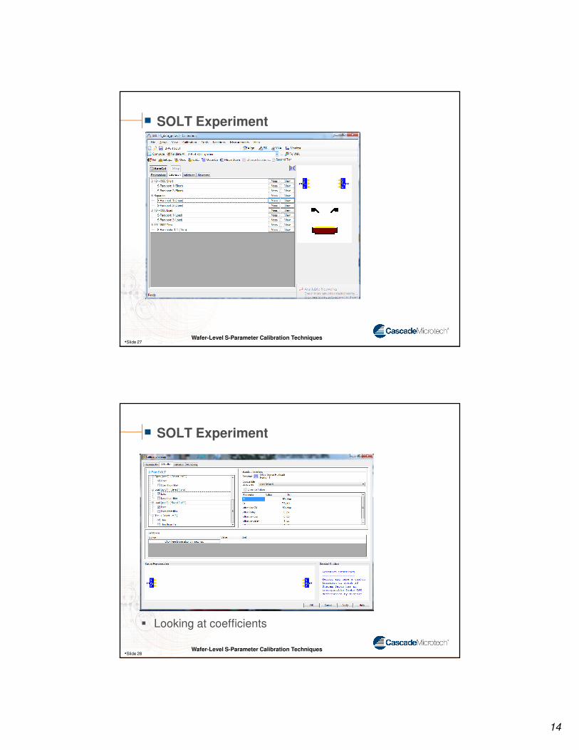
SOLT Experiment
Wincal settings loaded from file
Calibration settings loaded from file
Calibration populated with measurements and
calculated
Measurements of line standards carried out
•Slide 26
14
Wafer-Level S-Parameter Calibration Techniques
SOLT Experiment
•Slide 27
Wafer-Level S-Parameter Calibration Techniques
SOLT Experiment
Looking at coefficients
•Slide 28
15
Wafer-Level S-Parameter Calibration Techniques
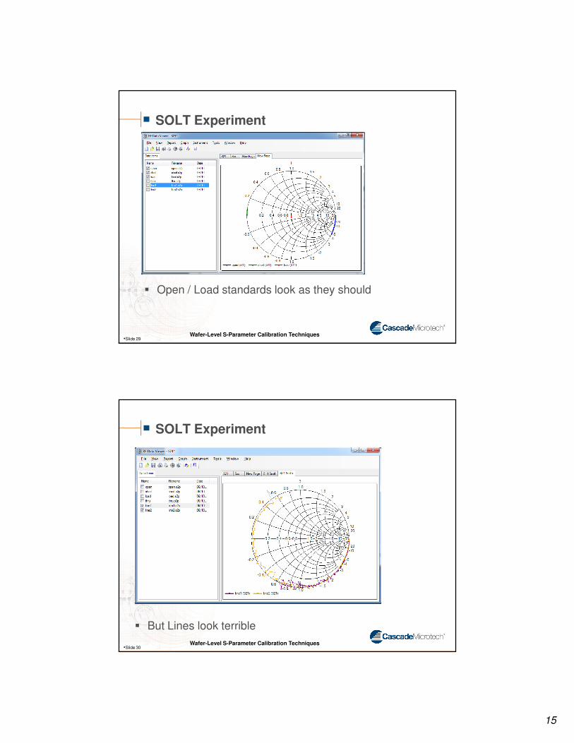
SOLT Experiment
Open / Load standards look as they should
•Slide 29
Wafer-Level S-Parameter Calibration Techniques
SOLT Experiment
But Lines look terrible
•Slide 30
16
Wafer-Level S-Parameter Calibration Techniques
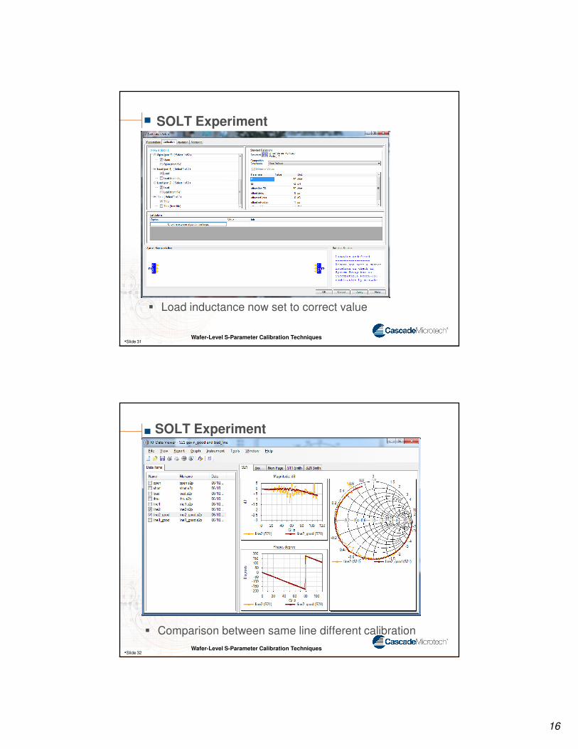
SOLT Experiment
Load inductance now set to correct value
•Slide 31
Wafer-Level S-Parameter Calibration Techniques
SOLT Experiment
Comparison between same line different calibration
•Slide 32
17
Wafer-Level S-Parameter Calibration Techniques
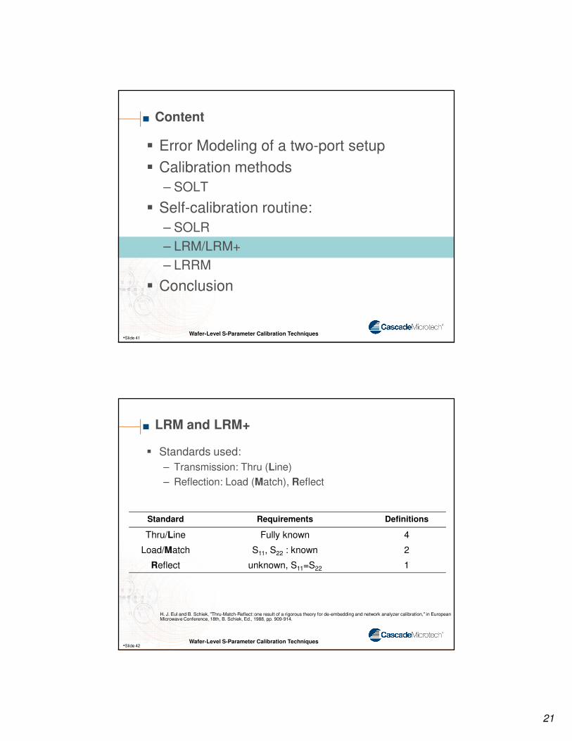
Content
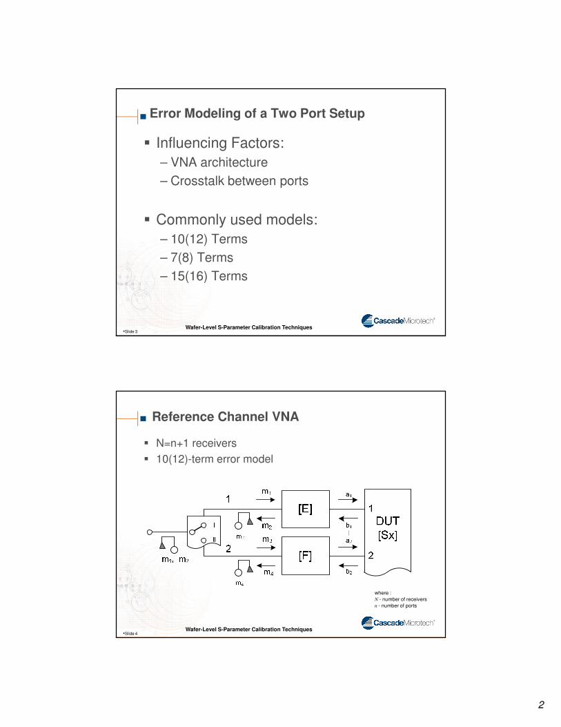
Error Modeling of a two-port setup
Calibration methods
– SOLT
Self-calibration routine:
– SOLR
– LRM/LRM+
– LRRM
Conclusion
•Slide 33
Wafer-Level S-Parameter Calibration Techniques
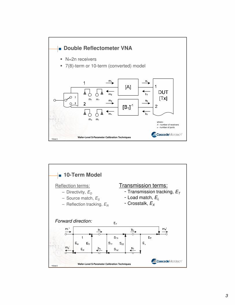
Self Calibration
Requires double reflectometer VNA
Two error matrices [A] and [B] of [T] parameters
7 error terms are in use (normalized to A22)
More information is measured than required
This additional information allows some parameters to be calculated from
within the calibration routine
•Slide 34
=
−
''
4
'
4
''
3
'
3
1
2221
1211
2221
1211
2221
1211
''
2
'
2
''
1
'
1
mm
mm
BB
BB
TT
TT
AA
AA
mm
mm
18
Wafer-Level S-Parameter Calibration Techniques
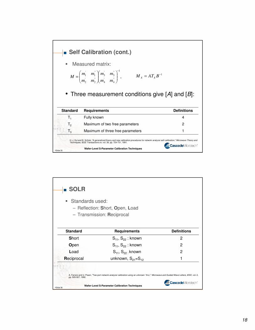
Self Calibration (cont.)
Measured matrix:
•Slide 35
1−= BATM
XX,
1
''
4
'
4
''
3
'
3
''
2
'
2
''
1
'
1
−
=
mm
mm
mm
mmM
• Three measurement conditions give [A] and [B]:
Standard Requirements Definitions
T1 Fully known 4
T2 Maximum of two free parameters 2
T3 Maximum of three free parameters 1
H. J. Eul and B. Schiek, "A generalized theory and new calibration procedures for network analyzer self-calibration," Microwave Theory and Techniques, IEEE Transactions on, vol. 39, pp. 724-731, 1991.
Wafer-Level S-Parameter Calibration Techniques
SOLR
Standards used:
– Reflection: Short, Open, Load
– Transmission: Reciprocal
•Slide 36
Standard Requirements Definitions
Short S11, S22 : known 2
Open S11, S22 : known 2
Load S11, S22 : known 2
Reciprocal unknown, S21=S12 1
A. Ferrero and U. Pisani, "Two-port network analyzer calibration using an unknown `thru'," Microwave and Guided Wave Letters, IEEE, vol. 2, pp. 505-507, 1992.
– Define extracted data-file models for OSL standards
Observation
– SOLR is as good as you know your OSL standards
•Slide 38
20
Wafer-Level S-Parameter Calibration Techniques
SOLR Experiment
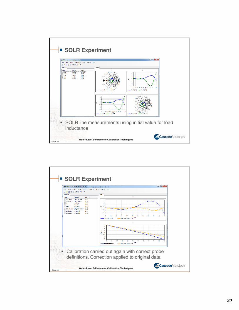
SOLR line measurements using initial value for load
inductance
•Slide 39
Wafer-Level S-Parameter Calibration Techniques
SOLR Experiment
Calibration carried out again with correct probe
definitions. Correction applied to original data
•Slide 40
21
Wafer-Level S-Parameter Calibration Techniques
Content
Error Modeling of a two-port setup
Calibration methods
– SOLT
Self-calibration routine:
– SOLR
– LRM/LRM+
– LRRM
Conclusion
•Slide 41
Wafer-Level S-Parameter Calibration Techniques
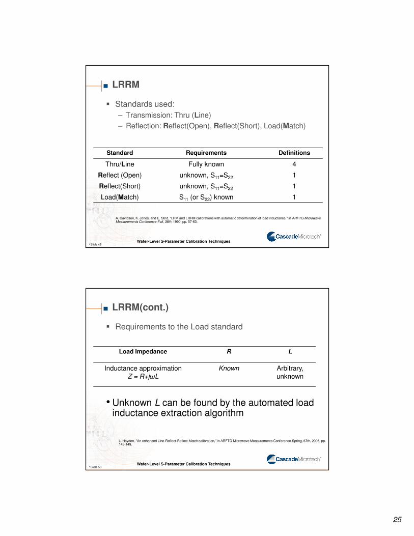
LRM and LRM+
Standards used:
– Transmission: Thru (Line)
– Reflection: Load (Match), Reflect
•Slide 42
Standard Requirements Definitions
Thru/Line Fully known 4
Load/Match S11, S22 : known 2
Reflect unknown, S11=S22 1
H. J. Eul and B. Schiek, "Thru-Match-Reflect: one result of a rigorous theory for de-embedding and network analyzer calibration," in European Microwave Conference, 18th, B. Schiek, Ed., 1988, pp. 909-914.
22
Wafer-Level S-Parameter Calibration Techniques
LRM vs. LRM+
Differ in requirements for Load standard:
– LRM for coaxial applications
– LRM+ for on-wafer calibration
•Slide 43
Method Load R X
LRM Known R1=R2=50Ω 0
LRM+ Known R1, R2
Arbitrary
X1, X2
Arbitrary
R. F. Scholz, F. Korndorfer, B. Senapati, and A. Rumiantsev, "Advanced technique for broadband on-wafer RF device characterization," in ARFTG Microwave Measurements Conference-Spring, 63rd, 2004, pp. 83-90.
Wafer-Level S-Parameter Calibration Techniques
Experiment
LRM/LRM+
•Slide 44
23
Wafer-Level S-Parameter Calibration Techniques
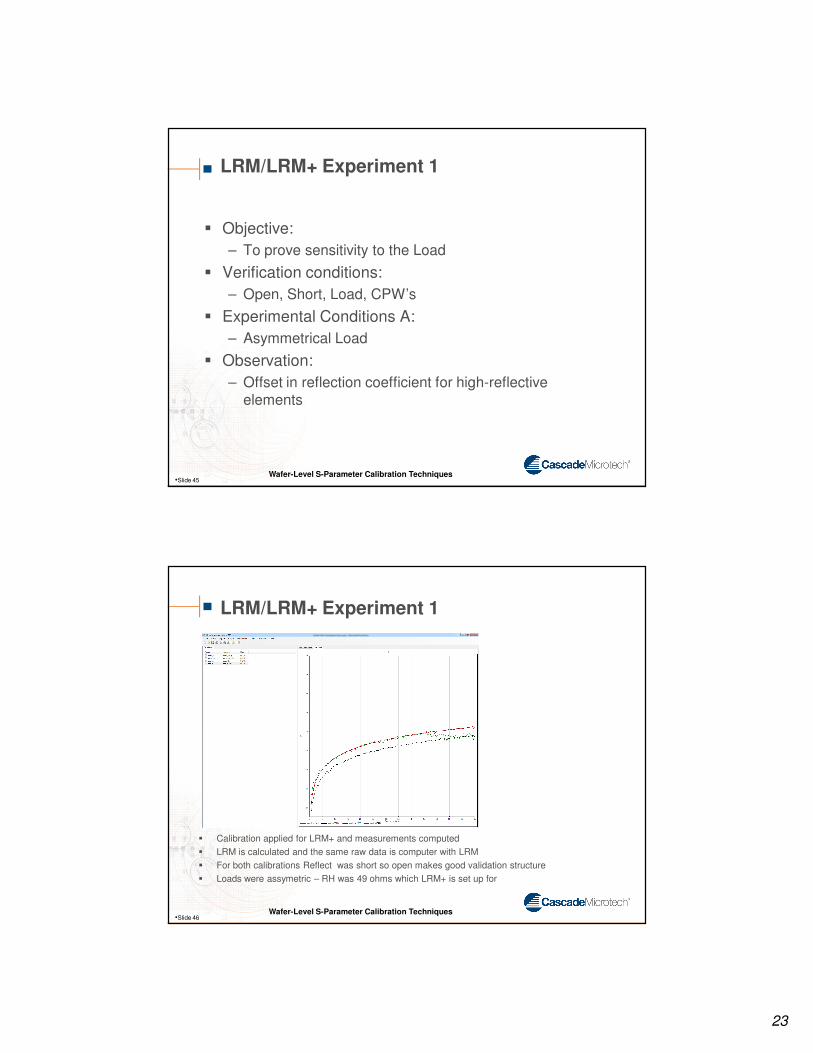
LRM/LRM+ Experiment 1
Objective:
– To prove sensitivity to the Load
Verification conditions:
– Open, Short, Load, CPW’s
Experimental Conditions A:
– Asymmetrical Load
Observation:
– Offset in reflection coefficient for high-reflective elements
•Slide 45
Wafer-Level S-Parameter Calibration Techniques
LRM/LRM+ Experiment 1
Calibration applied for LRM+ and measurements computed
LRM is calculated and the same raw data is computer with LRM
For both calibrations Reflect was short so open makes good validation structure
Loads were assymetric – RH was 49 ohms which LRM+ is set up for
•Slide 46
24
Wafer-Level S-Parameter Calibration Techniques
LRM/LRM+ Experiment 1
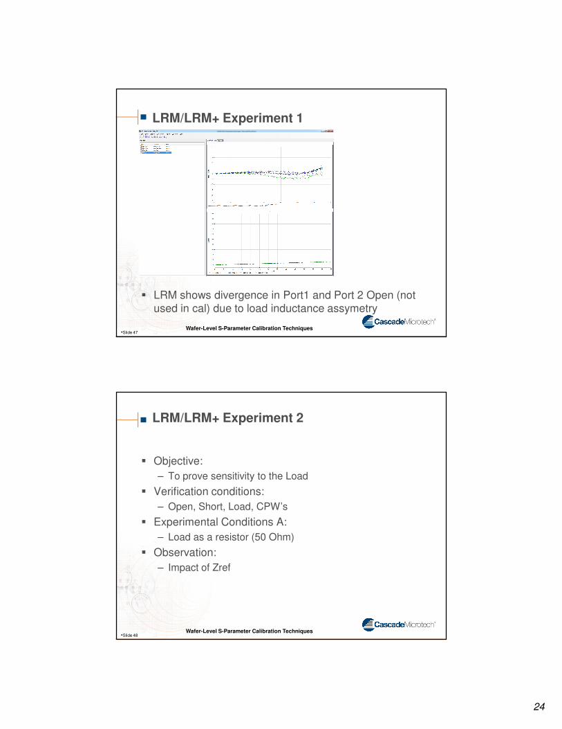
LRM shows divergence in Port1 and Port 2 Open (not
A. Davidson, K. Jones, and E. Strid, "LRM and LRRM calibrations with automatic determination of load inductance," in ARFTG Microwave Measurements Conference-Fall, 36th, 1990, pp. 57-63.
Wafer-Level S-Parameter Calibration Techniques
LRRM(cont.)
Requirements to the Load standard
•Slide 50
Load Impedance R L
Inductance approximation
Z = R+jωL
Known Arbitrary,
unknown
• Unknown L can be found by the automated load inductance extraction algorithm
L. Hayden, "An enhanced Line-Reflect-Reflect-Match calibration," in ARFTG Microwave Measurements Conference-Spring, 67th, 2006, pp. 143-149.
26
Wafer-Level S-Parameter Calibration Techniques
Experiment
LRRM
•Slide 51
Wafer-Level S-Parameter Calibration Techniques
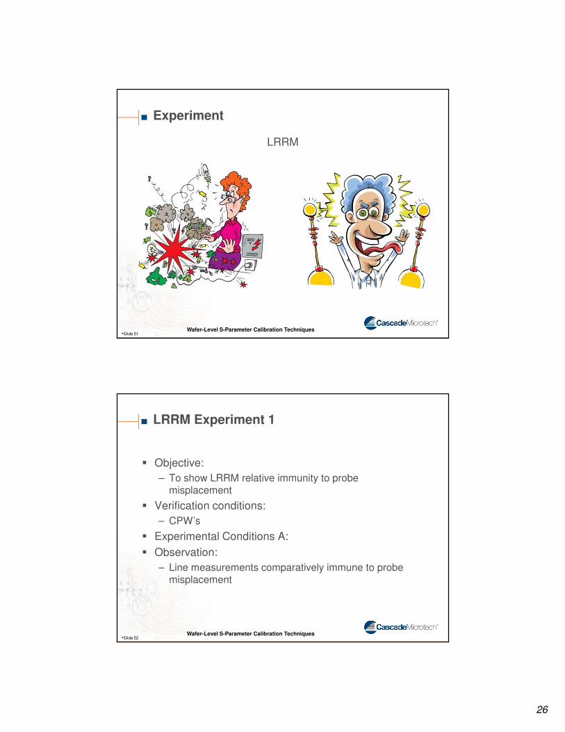
LRRM Experiment 1
Objective:
– To show LRRM relative immunity to probe misplacement
Verification conditions:
– CPW’s
Experimental Conditions A:
Observation:
– Line measurements comparatively immune to probe misplacement
•Slide 52
27
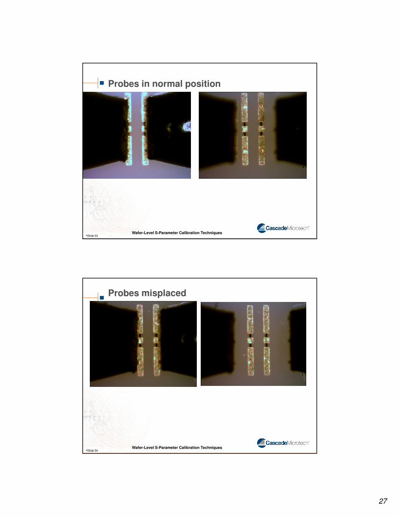
Wafer-Level S-Parameter Calibration Techniques
Probes in normal position
•Slide 53
Wafer-Level S-Parameter Calibration Techniques
Probes misplaced
•Slide 54
28
Wafer-Level S-Parameter Calibration Techniques
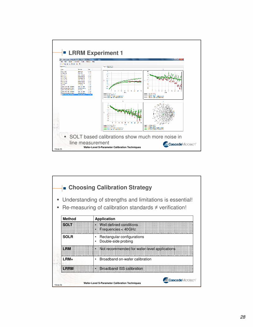
LRRM Experiment 1
SOLT based calibrations show much more noise in
line measurement•Slide 55
Wafer-Level S-Parameter Calibration Techniques
Choosing Calibration Strategy
Understanding of strengths and limitations is essential!
Re-measuring of calibration standards ≠ verification!
•Slide 56
Method Application
SOLT • Well defined conditions
• Frequencies < 40GHz
SOLR • Rectangular configurations
• Double-side probing
LRM • Not recommended for wafer-level applications