GCA AS200 Job Preparation The GCA AutoStep 200 wafer stepper is an easy to use instrument capable of very clean lithography with a typical resolution of 0.75 µm, and even 0.6 µm with some optimization. If you plan to use the wafer stepper, you must begin your job planning when you do the CAD layout for your chip. The stepper has a maximum exposure field 21 mm in diameter, with a maximum square of 14.85 mm, so the pattern you wish to expose in a single flash must be no larger than this. Ours is a 5X stepper so features on the reticle are five times larger than they will be on the wafer surface. The stepper uses a 5 inch reticle and special fiducial marks for aligning the reticle to the optical column. The GDS CAD files for the fiducial marks is available on the NDNF website. Identification barcodes are required on all new reticles. Routines are built-in to generate these barcodes on the 3600 Pattern Generator, and some outside vendors can do barcodes, but if your outside vendor cannot, you must add the barcodes yourself to your CAD layout. Contact Dr. Snider for help with this. RETICLE FIDUCIAL MARKS The fiducial marks are extremely important since the stepper’s reticle handling system automatically aligns the reticle to the optical column of the stepper. No manual alignment is possible. If the marks on your reticle are not correct, the stepper cannot do the alignment, and the reticle is useless. The fiducials, as shown in Fig. 1, consist of a 2 mm clear squares placed 117 mm apart (to the outside edges) in the y direction. Figure 1 shows three squares at the top and bottom, spaced on 11 mm centers. This is different than our old 6300 stepper. The AS 200 prefers to use marks that are offset in the x direction for better accuaracy. For now you can still use your old reticles in the AS200 but all new reticles should have 3 marks top and bottom. The 3600 PG can add these marks for you, but if your outside vendor cannot, then you will need to add them to your CAD. Figure 1. General reticle form.
Transcript
GCA AS200 Job Preparation The GCA AutoStep 200 wafer stepper is an easy to use instrument capable of very clean
lithography with a typical resolution of 0.75 µm, and even 0.6 µm with some optimization. If you plan to use the wafer stepper, you must begin your job planning when you do the CAD layout for your chip. The stepper has a maximum exposure field 21 mm in diameter, with a maximum square of 14.85 mm, so the pattern you wish to expose in a single flash must be no larger than this. Ours is a 5X stepper so features on the reticle are five times larger than they will be on the wafer surface. The stepper uses a 5 inch reticle and special fiducial marks for aligning the reticle to the optical column. The GDS CAD files for the fiducial marks is available on the NDNF website. Identification barcodes are required on all new reticles. Routines are built-in to generate these barcodes on the 3600 Pattern Generator, and some outside vendors can do barcodes, but if your outside vendor cannot, you must add the barcodes yourself to your CAD layout. Contact Dr. Snider for help with this.
RETICLE FIDUCIAL MARKS The fiducial marks are extremely important since the stepper’s reticle handling system
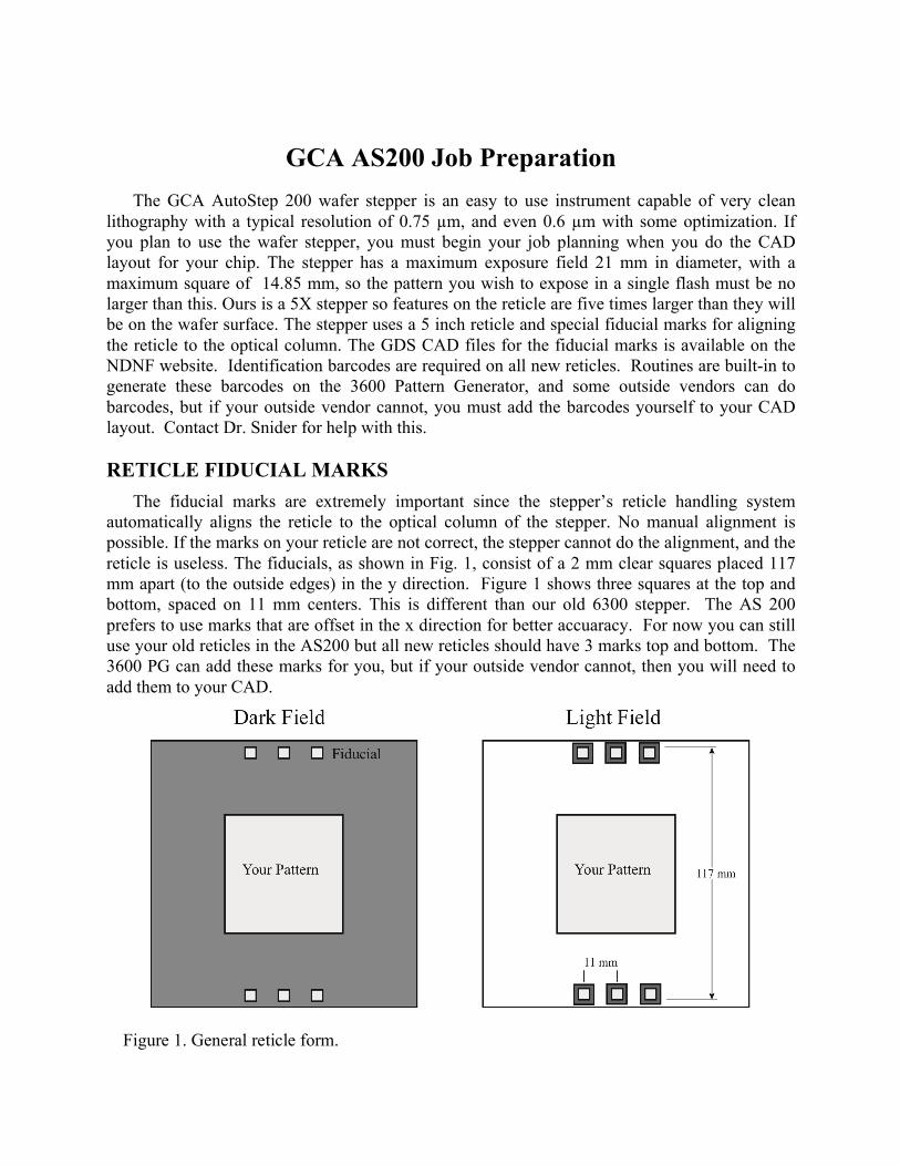
automatically aligns the reticle to the optical column of the stepper. No manual alignment is possible. If the marks on your reticle are not correct, the stepper cannot do the alignment, and the reticle is useless. The fiducials, as shown in Fig. 1, consist of a 2 mm clear squares placed 117 mm apart (to the outside edges) in the y direction. Figure 1 shows three squares at the top and bottom, spaced on 11 mm centers. This is different than our old 6300 stepper. The AS 200 prefers to use marks that are offset in the x direction for better accuaracy. For now you can still use your old reticles in the AS200 but all new reticles should have 3 marks top and bottom. The 3600 PG can add these marks for you, but if your outside vendor cannot, then you will need to add them to your CAD.
Figure 1. General reticle form.
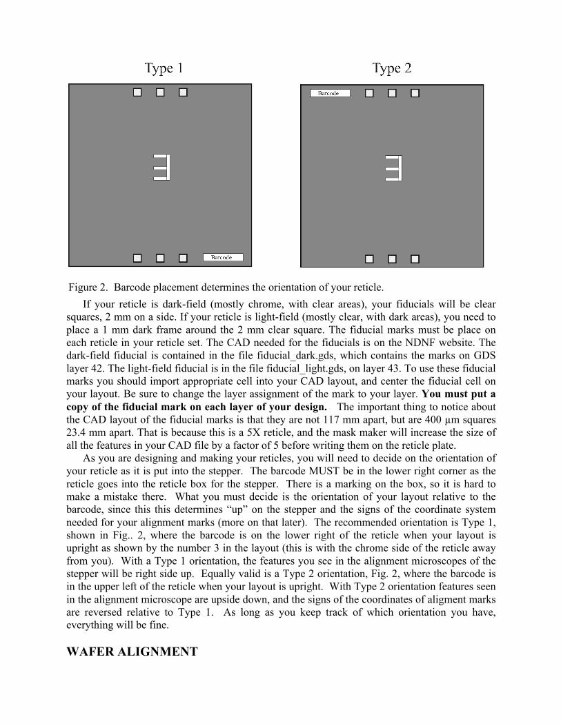
If your reticle is dark-field (mostly chrome, with clear areas), your fiducials will be clear squares, 2 mm on a side. If your reticle is light-field (mostly clear, with dark areas), you need to place a 1 mm dark frame around the 2 mm clear square. The fiducial marks must be place on each reticle in your reticle set. The CAD needed for the fiducials is on the NDNF website. The dark-field fiducial is contained in the file fiducial_dark.gds, which contains the marks on GDS layer 42. The light-field fiducial is in the file fiducial_light.gds, on layer 43. To use these fiducial marks you should import appropriate cell into your CAD layout, and center the fiducial cell on your layout. Be sure to change the layer assignment of the mark to your layer. You must put a copy of the fiducial mark on each layer of your design. The important thing to notice about the CAD layout of the fiducial marks is that they are not 117 mm apart, but are 400 µm squares 23.4 mm apart. That is because this is a 5X reticle, and the mask maker will increase the size of all the features in your CAD file by a factor of 5 before writing them on the reticle plate.
As you are designing and making your reticles, you will need to decide on the orientation of your reticle as it is put into the stepper. The barcode MUST be in the lower right corner as the reticle goes into the reticle box for the stepper. There is a marking on the box, so it is hard to make a mistake there. What you must decide is the orientation of your layout relative to the barcode, since this this determines “up” on the stepper and the signs of the coordinate system needed for your alignment marks (more on that later). The recommended orientation is Type 1, shown in Fig.. 2, where the barcode is on the lower right of the reticle when your layout is upright as shown by the number 3 in the layout (this is with the chrome side of the reticle away from you). With a Type 1 orientation, the features you see in the alignment microscopes of the stepper will be right side up. Equally valid is a Type 2 orientation, Fig. 2, where the barcode is in the upper left of the reticle when your layout is upright. With Type 2 orientation features seen in the alignment microscope are upside down, and the signs of the coordinates of aligment marks are reversed relative to Type 1. As long as you keep track of which orientation you have, everything will be fine.
WAFER ALIGNMENT
Figure 2. Barcode placement determines the orientation of your reticle.
If your pattern has only one layer of lithography, you are very lucky: you don’t need to worry about any alignment. If you have more than one layer of lithography, you will need to consider the stepper alignment scheme when doing your layout. There must always be an alignment mark on the first layer, and additional alignment marks can be added to subsequent layers. There is a special alignment mark, called a snowflake, that matches marks built into the GCA microscope system. The stepper is capable of great flexibility in placement of the alignment marks on your wafers, but there is a trade-off between flexibility and simplicity.
In aligning the exposure to a pre-existing pattern on the wafer, two marks (or alignment keys) are needed to define correct rotational and x-y alignment. The stepper uses two microscope objectives placed 63.5 mm apart to display the alignment marks on the stepper monitor. The simplest alignment scheme has marks this distance apart, so that two alignment marks appear
simultaneously. This makes rotational and x-y alignment easy. Marks with this spacing are called “Standard Keys”. The most important thing to remember about alignment marks are that the stepper uses the right alignment mark to define the x-y placement of the die, while the only purpose of the left mark is so the user can set the rotational alignment. Once the alignment is done on the stepper monitor screen, the wafer is properly aligned to the motions of the stage, and the stepper “knows” the location of a mark on the wafer (the right alignment mark). The exposure job must then tell the stepper where to place the exposures relative to this mark. To allow the user maximum flexibility in the exposure pattern of the wafer, the user can define parameters that determine where the pattern is exposed on the wafer: the size of the
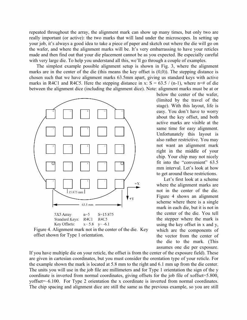
array of exposures, the step (in x and y) between exposure flashes, and the offset of the center of the nearest die to the magic “known” location (or mark) on the wafer. The array and step size is easily understood. The offset, called the “Key Offset”, is tougher to understand, but to make it easy for the user the stepper does all the tough math, and all you have to do is define the vector between the center of your die, and the center of the alignment mark. Since the exposure is
Figure 3. Sample die and mark arrangement.
repeated throughout the array, the alignment mark can show up many times, but only two are really important (or active): the two marks that will land under the microscopes. In setting up your job, it’s always a good idea to take a piece of paper and sketch out where the die will go on the wafer, and where the alignment marks will be. It’s very embarrassing to have your reticles made and then find out that your die placement cannot be as you expected. Be especially careful with very large die. To help you understand all this, we’ll go through a couple of examples.
The simplest example possible alignment setup is shown in Fig. 3, where the alignment marks are in the center of the die (this means the key offset is (0,0)). The stepping distance is chosen such that we have alignment marks 63.5mm apart, giving us standard keys with active marks in R4C1 and R4C5. Here the stepping distance in x: S = 63.5 / (n-1), where n=# of die between the alignment dice (including the alignment dice). Note: alignment marks must be at or
below the center of the wafer, (limited by the travel of the stage). With this layout, life is easy. You don’t have to worry about the key offset, and both active marks are visible at the same time for easy alignment. Unfortunately this layout is also rather restrictive. You may not want an alignment mark right in the middle of your chip. Your chip may not nicely fit into the “convenient” 63.5 mm interval. Let’s look at how to get around these restrictions.
Let’s first look at a scheme where the alignment marks are not in the center of the die. Figure 4 shows an alignment scheme where there is a single mark in each die, but it is not in the center of the die. You tell the stepper where the mark is using the key offset in x and y, which are the components of the vector from the center of the die to the mark. (This assumes one die per exposure.
If you have multiple die on your reticle, the offset is from the center of the exposure field). These are given in cartesian coordinates, but you must consider the orentation type of your reticle. For the example shown the mark is located at 5.8 mm to the right and 6.1 mm up from the die center. The units you will use in the job file are millimeters and for Type 1 orientation the sign of the y coordinate is inverted from normal coordinates, giving offsets for the job file of xoffset=5.800, yoffset=–6.100. For Type 2 orientation the x coordinate is inverted from normal coordinates. The chip spacing and alignment dice are still the same as the previous example, so you are still
Figure 4. Alignment mark not in the center of the die. Key offset shown for Type 1 orientation.
using standard keys. Even though the marks are now offset, the array will still be centered on the wafer. When you run your job, the stepper moves the wafer to the alignment position, adding in the key offsets so that the alignment marks will appear on the screens.
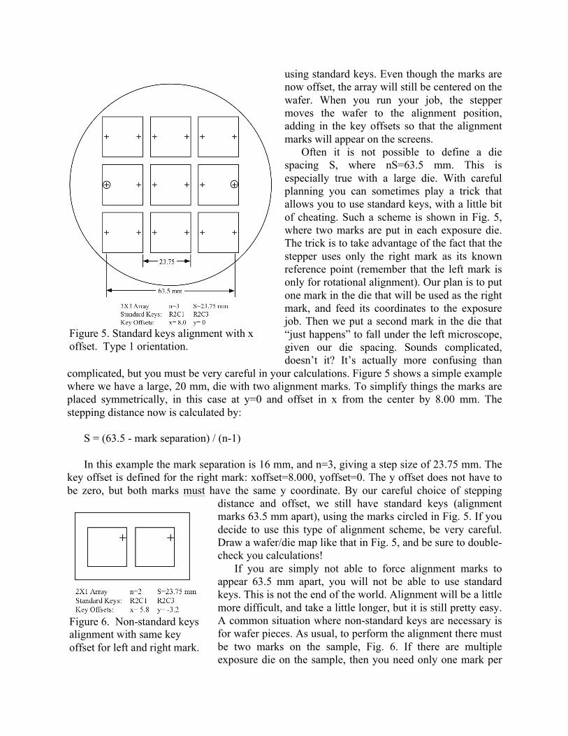
Often it is not possible to define a die spacing S, where nS=63.5 mm. This is especially true with a large die. With careful planning you can sometimes play a trick that allows you to use standard keys, with a little bit of cheating. Such a scheme is shown in Fig. 5, where two marks are put in each exposure die. The trick is to take advantage of the fact that the stepper uses only the right mark as its known reference point (remember that the left mark is only for rotational alignment). Our plan is to put one mark in the die that will be used as the right mark, and feed its coordinates to the exposure job. Then we put a second mark in the die that “just happens” to fall under the left microscope, given our die spacing. Sounds complicated, doesn’t it? It’s actually more confusing than
complicated, but you must be very careful in your calculations. Figure 5 shows a simple example where we have a large, 20 mm, die with two alignment marks. To simplify things the marks are placed symmetrically, in this case at y=0 and offset in x from the center by 8.00 mm. The stepping distance now is calculated by:
S = (63.5 - mark separation) / (n-1)
In this example the mark separation is 16 mm, and n=3, giving a step size of 23.75 mm. The key offset is defined for the right mark: xoffset=8.000, yoffset=0. The y offset does not have to be zero, but both marks must have the same y coordinate. By our careful choice of stepping
distance and offset, we still have standard keys (alignment marks 63.5 mm apart), using the marks circled in Fig. 5. If you decide to use this type of alignment scheme, be very careful. Draw a wafer/die map like that in Fig. 5, and be sure to double-check you calculations!
If you are simply not able to force alignment marks to appear 63.5 mm apart, you will not be able to use standard keys. This is not the end of the world. Alignment will be a little more difficult, and take a little longer, but it is still pretty easy. A common situation where non-standard keys are necessary is for wafer pieces. As usual, to perform the alignment there must be two marks on the sample, Fig. 6. If there are multiple exposure die on the sample, then you need only one mark per
Figure 5. Standard keys alignment with x offset. Type 1 orientation.
Figure 6. Non-standard keys alignment with same key offset for left and right mark.
die. If there is only one exposure die, then you must include two marks. For simplicity, it is a good idea to have marks with the same y coordinate.
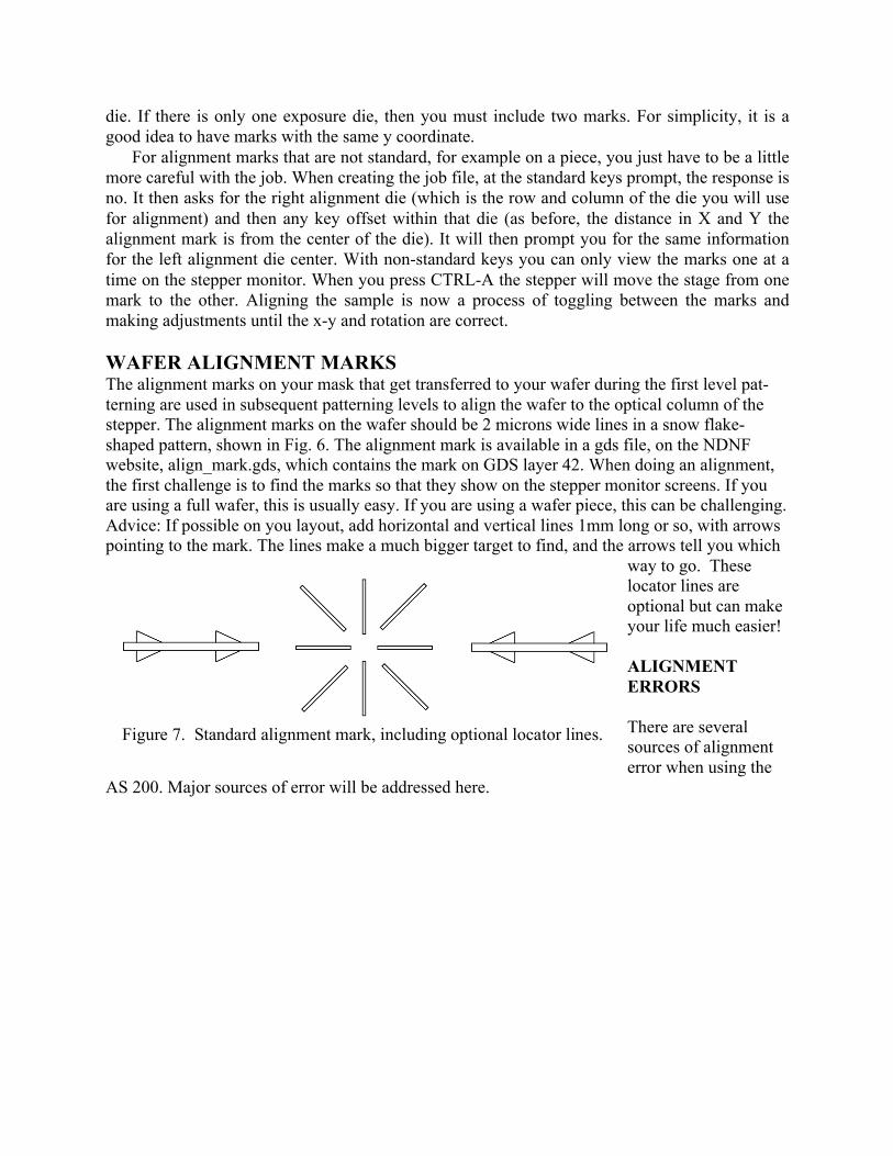
For alignment marks that are not standard, for example on a piece, you just have to be a little more careful with the job. When creating the job file, at the standard keys prompt, the response is no. It then asks for the right alignment die (which is the row and column of the die you will use for alignment) and then any key offset within that die (as before, the distance in X and Y the alignment mark is from the center of the die). It will then prompt you for the same information for the left alignment die center. With non-standard keys you can only view the marks one at a time on the stepper monitor. When you press CTRL-A the stepper will move the stage from one mark to the other. Aligning the sample is now a process of toggling between the marks and making adjustments until the x-y and rotation are correct. WAFER ALIGNMENT MARKS The alignment marks on your mask that get transferred to your wafer during the first level pat-terning are used in subsequent patterning levels to align the wafer to the optical column of the stepper. The alignment marks on the wafer should be 2 microns wide lines in a snow flake-shaped pattern, shown in Fig. 6. The alignment mark is available in a gds file, on the NDNF website, align_mark.gds, which contains the mark on GDS layer 42. When doing an alignment, the first challenge is to find the marks so that they show on the stepper monitor screens. If you are using a full wafer, this is usually easy. If you are using a wafer piece, this can be challenging. Advice: If possible on you layout, add horizontal and vertical lines 1mm long or so, with arrows pointing to the mark. The lines make a much bigger target to find, and the arrows tell you which
way to go. These locator lines are optional but can make your life much easier! ALIGNMENT ERRORS There are several sources of alignment error when using the
AS 200. Major sources of error will be addressed here.
Figure 7. Standard alignment mark, including optional locator lines.
1. Alignment errors of the mask to the column Since the reticle is automatically aligned to the optical column, this error is usually small,
typically less than 0.1 µm. 2. Alignment errors of the wafer to the column
The accuracy of this alignment is the responsibility of the user. Perfect alignment of the 2 µm with the marks on the screen leaves 0.5 µm on each side. Thus a worst case error is typically 0.5 µm. If you use automatic local alignment (µDFAS) this error can be much less. 3. Stage error
Positional precision of the stage is ±0.1 µm. 4. Calibration error
Several times a week, the steppers are calibrated with a test pattern to set the alignment between the stage and the microscopes. This is known as the baseline. A typical error range for the baseline is between 0.0 and 0.15 µm. When all of the types of errors are added together, the typical alignment accuracy is around ± 0.25 microns. Keep this in mind when designing your device. STEPPER COMMANDS Accounts have been set-up for the primary research groups. If you do not have access to an account on the stepper, contact Mark Richmond, who will give you access to one. The following is a list of the common commands that you will use. LOG IN [##,&&] - to log into the stepper. The first two numbers, ## define the research group and the second numbers define the user. For instance [42,1] is the ICFab undergrad account and [42,2] is the ICFab grad account. You will be asked for the account password to complete the login. SPEC - to create or specify a job. More details will be given later. EDIT - to edit an existing job. LISTF - to list the files in the directory. DELETE - to delete an existing file. EXEC - to run a job. It will prompt you for the job name and pass. A shortcut is to type it all at once, i.e. EXEC job name\pass. EXPO - to run an exposure or an exposure/focus test for process characterization. See the exposure section for more details. MAP – to map the wafer for local alignment. Generally used when exposing a wafer with local alignment.
RMSRET – returns the reticle on the optical column back to the elevator. LOG OUT - to sign-off the stepper MISCELLANEOUS COMMANDS Here is a short list of other stepper commands that may prove handy: (see the stepper manual for more) LOAD - puts the stage back into the wafer loading position. RMSL – sets the reticle management system into the load state so that you can change reticles in the elevator. ORIG - retunes the laser and originates the stage laser metering. COPY - copy files. This can also be from another user’s directory. RENAME - gives an existing file a new name ? - typing “?” followed by a carriage return will back you up one line at a time in the SPEC or EDIT mode EXPOSURE
The first thing to be aware of is the thickness limits of the stepper. There are four chucks, one for 25 mil (600 µm) thick 4 inch wafers, and another for 400 µm thick 4 inch wafers, and two for piece parts. The focus on the stepper can change by XXXX. If your wafer is much thicker or thinner than the range allowed by the two chucks the stepper may not be able to focus. Check with Mike Thomas or Mark Richmond if you have an unusual wafer.
Depending on the design, thickness of the resist and wafer type, a characterization should be done to determine the best exposure time and focus value. The command EXPO is used to auto¬matically create an array of different exposure conditions. EXPO can be used in two ways. 1. It can be used as an exposure/focus matrix that uses an array from an existing job. Each row is a different focus value and each column is a different exposure time. 2. EXPO can also be used to create a matrix where only the exposure time is varied. An important issue to be aware of is the order in which the stepper exposes the die, as shown below.
To execute a matrix, type EXPO Jobname\Passname. To specify the focus/exposure matrix,
at the prompt of A-rray or R-ow, type R. If the exposure only matrix is wanted, type A. The step-per will then ask for the exposure range, and if needed the focus range. The rest of exposure
steps are the same as executing a regular job. After the stepper is done exposing the matrix, remove your wafer, but do not type anything on the keyboard. Develop your wafer, and inspect it under a microscope to determine the best die. Return to the stepper and give the row and column coordinates of the best die. Stepper will give the focus and exposure numbers for that die.
OTHER TIPS: If you get a FOCUS ERROR, there are a number of possible causes:
- is your wafer too thick or thin? (most wafers are nominal ± l0 mils) - check to make sure the piece is centered on the chuck - check to see if there is any residue on the backside - clean it! - make sure the chuck is set correctly on the stage, i.e. it is flat?
If you get a TIME-OUT error:
- check to see if the lamp is on by looking.at the housing.(should see light reflecting from the top back) If not, the bulb is off or burned out. Call Mike Thomas.
- the exposure value is too long. If this error appears, try a shorter time and run the pass sev-eral times to get desired exposure time.
If you get a LIGHT TOO LOW error:
- the exposure value may be too long - see TIME-OUT error
Exposure Job Setup This is a short version of the job setup command. Section 5 and 6 of the system control man-
ual has more details if they are needed. Usually the easiest thing to do is to copy and existing job and edit it to do what you need. To edit and existing job use the command EDIT, while to start a job from scratch, use SPEC. In either case, the computer will ask you a series of questions, and your responses will be used to create the job file. SPEC Output job name: your choice Metric or English(*M/E): * indicates default Job Comment: Tolerance (1,2,*3, 4, 5,6): Scale Corrections See section 5 of manual
X, PPM (-200 +200) Y, PPM (-200 +200)
Orthogonality, PPM (-128 +128) See section 5 Leveler batch size [1-25] Level every so many wafers (usually 1) Wafer Diameter in mm «Array Parameters» Step in X: in mm
*C -ount, S -pan or A -ll: Count-specify # of columns; Span - How Wide? (prompt if S is
chosen)spans desired width;
All Fills all possible locations How Many Columns? (prompt for Count) available width. Step in Y: in mm
*C -ount, S -pan, A -ll: How High? (Span) How Many Rows? (Column) Translate Origin Translates the whole array in X or Y
In X: In Y:
Display? (Y/*N) For a Y answer, shows array of exposures; indicates if std keys
Pass # Array 24 exposures total exposures =24 1 2 3 4 5 6 1 X X 2 X X X X 3 X X X X X X 4 X X X X X X 5 X X X X 6 X X
Alignment Dice are Standard R:4 C:6 R:4 C:1
Layout? (Y/*N) Position of exposures
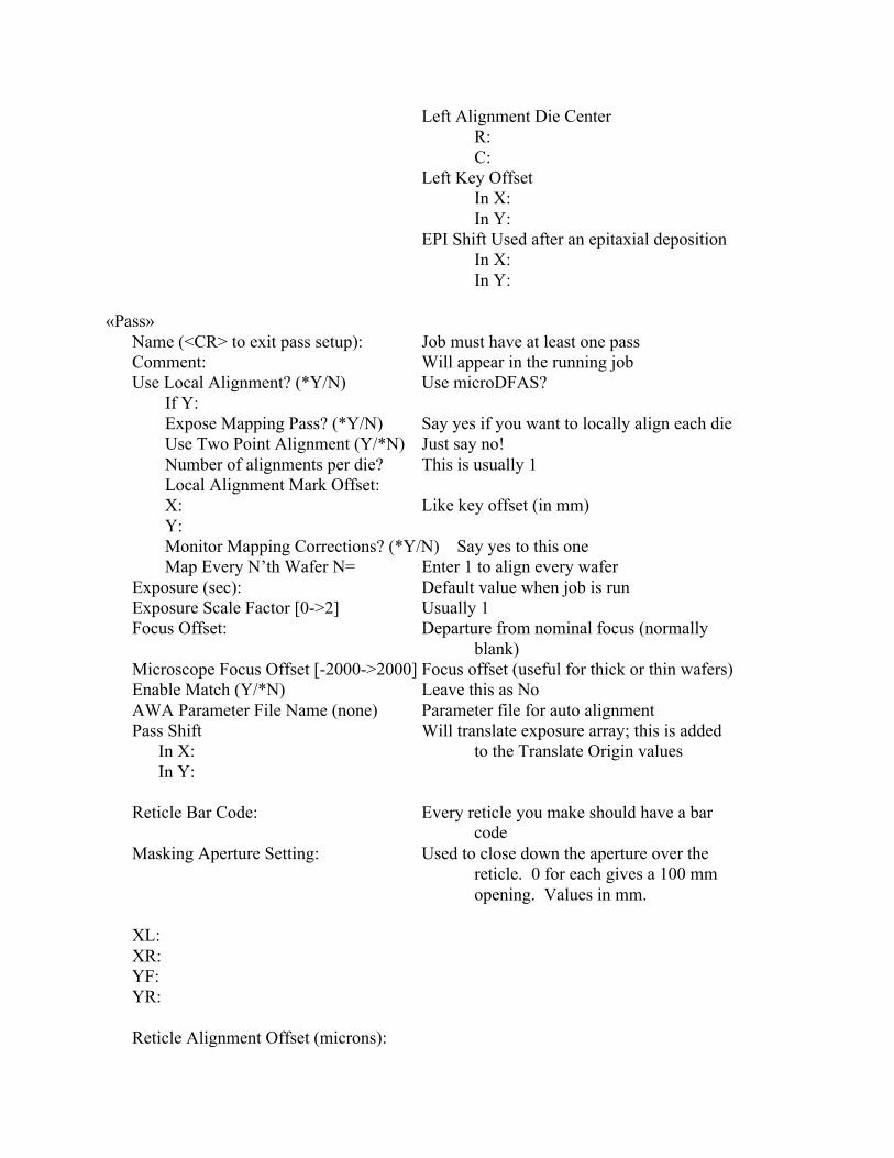
For a Y answer, the output is: Array has: Centered: 6 rows 3,4 6 columns 3, 4 1st row, col: X = –31.75000 Y=–31.75000 «Alignment Parameters» Standard Keys? (*Y/N) Yes if keys are 63.5 mm apart, offset in mm Prompts for Y Prompts for N Right Key Offset Right Alignment Die Center
In X: R: In Y: C:
EPI Shift Key Offset In X: In X: In Y: In Y: If not standard keys:
Left Alignment Die Center R: C: Left Key Offset In X: In Y: EPI Shift Used after an epitaxial deposition In X: In Y:
«Pass»
Name (<CR> to exit pass setup): Job must have at least one pass Comment: Will appear in the running job Use Local Alignment? (*Y/N) Use microDFAS? If Y: Expose Mapping Pass? (*Y/N) Say yes if you want to locally align each die Use Two Point Alignment (Y/*N) Just say no! Number of alignments per die? This is usually 1 Local Alignment Mark Offset: X: Like key offset (in mm) Y: Monitor Mapping Corrections? (*Y/N) Say yes to this one Map Every N’th Wafer N= Enter 1 to align every wafer Exposure (sec): Default value when job is run Exposure Scale Factor [0->2] Usually 1 Focus Offset: Departure from nominal focus (normally blank) Microscope Focus Offset [-2000->2000] Focus offset (useful for thick or thin wafers) Enable Match (Y/*N) Leave this as No AWA Parameter File Name (none) Parameter file for auto alignment Pass Shift Will translate exposure array; this is added In X: to the Translate Origin values In Y:
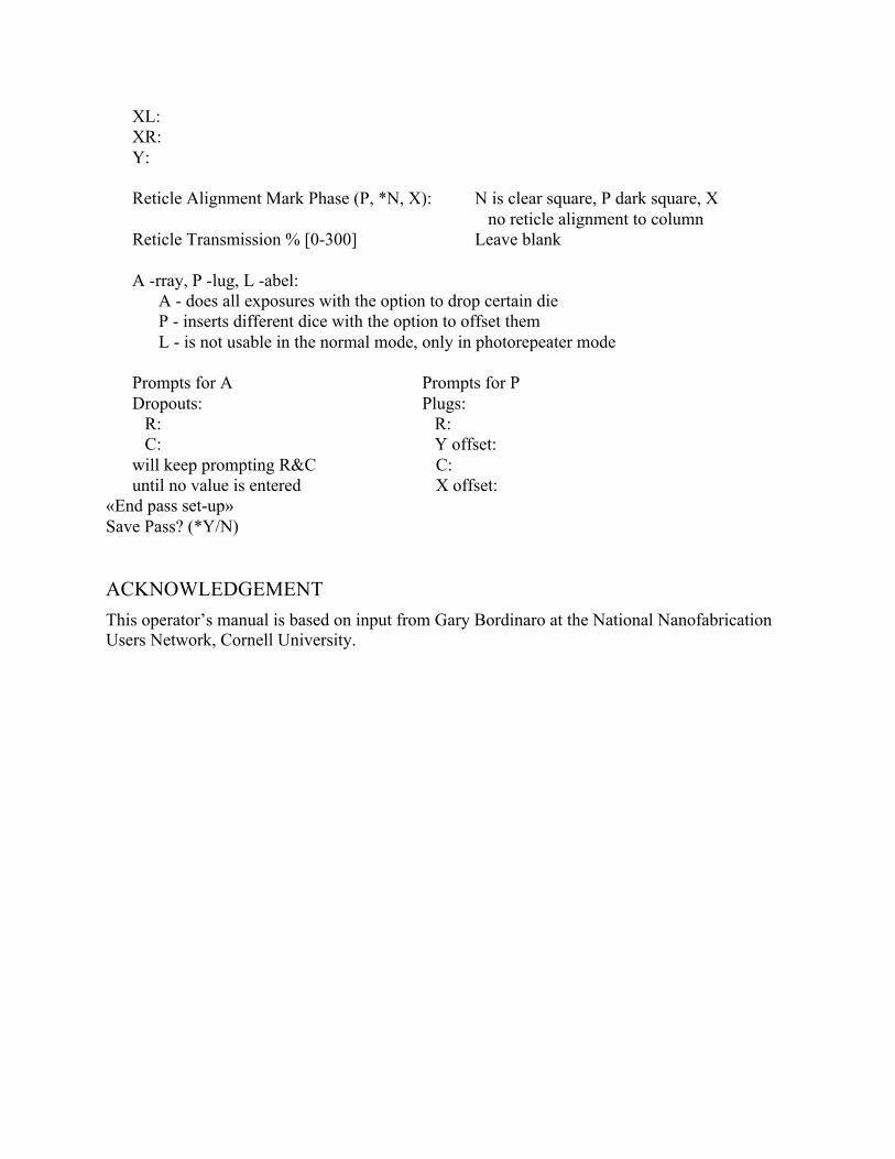
Reticle Bar Code: Every reticle you make should have a bar code Masking Aperture Setting: Used to close down the aperture over the reticle. 0 for each gives a 100 mm opening. Values in mm. XL: XR: YF: YR:
Reticle Alignment Offset (microns):
XL: XR: Y:
Reticle Alignment Mark Phase (P, *N, X): N is clear square, P dark square, X
no reticle alignment to column Reticle Transmission % [0-300] Leave blank
A -rray, P -lug, L -abel: A - does all exposures with the option to drop certain die P - inserts different dice with the option to offset them L - is not usable in the normal mode, only in photorepeater mode
Prompts for A Prompts for P Dropouts: Plugs:
R: R: C: Y offset:
will keep prompting R&C C: until no value is entered X offset:
«End pass set-up» Save Pass? (*Y/N)
ACKNOWLEDGEMENT This operator’s manual is based on input from Gary Bordinaro at the National Nanofabrication Users Network, Cornell University.