170
I/O Unit - Model A Connection Maintenance Manual Computer Numerical Controls GE Fanuc Automation Europe TECHNOLOGY AND MORE B-63 813EN/03

I/O Unit - Model A Connection
Maintenance Manual
Computer Numerical Controls
GE Fanuc Automation Europe
TECHNOLOGY ANDMORE
B-63813EN/03


B-61813E/03 DEFINITION OF WARNING, CAUTION, AND NOTE
s-1
DEFINITION OF WARNING, CAUTION, AND NOTEThis manual includes safety precautions for protecting the user andpreventing damage to the machine. Precautions are classified intoWarning and Caution according to their bearing on safety. Also,supplementary information is described as a Note. Read the Warning,Caution, and Note thoroughly before attempting to use the machine.
WARNINGApplied when there is a danger of the user beinginjured or when there is a damage of both the userbeing injured and the equipment being damaged ifthe approved procedure is not observed.
CAUTIONApplied when there is a danger of the equipment beingdamaged, if the approved procedure is not observed.
NOTEThe Note is used to indicate supplementaryinformation other than Warning and Caution.
• Read this manual carefully, and store it in a safe place.


B-61813E/03 PREFACE
p-1
PREFACEThis manual describe the following products:
Applicable modelsName of products Abbreviation
FANUC I/O Unit-MODEL A I/O Unit-AFANUC I/O Unit-MODEL B I/O Unit-B
Applicable CNCsName of products Abbreviation
FANUC Power Mate-MODEL A Power Mate-AFANUC Power Mate-MODEL B Power Mate-BFANUC Power Mate-MODEL C Power Mate-CFANUC Series 0(MODEL C) Series 0-CFANUC Series 15 Series 15FANUC Series 16 Series 16FANUC Series 18 Series 18FANUC SYSTEM F-MODEL D Mate F-D Mate


B-61813E/03
c-1
PREFACE
I CONNECTIONS
1. FANUC I/O LINK.............................................................................................................31.1 CONFIGURATION......................................................................................................................... 41.2 ALLOCATION OF I/O POINTS...................................................................................................... 5
2. I/O UNIT CONFIGURATION...........................................................................................8
3. INSTALLATION ..............................................................................................................93.1 ENVIRONMENTAL CONDITIONS ................................................................................................ 93.2 DESIGNING CONDITION FOR A CABINET............................................................................... 103.3 OUTER DIMENSION OF I/O Unit................................................................................................ 113.4 MOUNTING AND DISMOUNTING MODULES ........................................................................... 13
4. CONNECTION..............................................................................................................144.1 GENERAL CONNECTION DIAGRAM......................................................................................... 144.2 CONNECTING INPUT POWER SOURCE.................................................................................. 154.3 GROUNDING............................................................................................................................... 164.4 REQUIRED CURRENT ............................................................................................................... 174.5 INTERFACE MODULE (AIF01A, AIF01B)................................................................................... 184.6 INTERFACE MODULE (AIF02C) CONNECTION ....................................................................... 21
4.6.1 Overview ..............................................................................................................................................214.6.2 Connection...........................................................................................................................................224.6.3 Setting with the DIP switch ..................................................................................................................24
4.7 CONNECTING WITH I/O MODULES.......................................................................................... 25
5. DIGITAL INPUT / OUTPUT MODULES........................................................................275.1 LIST OF MODULES..................................................................................................................... 275.2 CORRESPONDENCE BETWEEN I/O SIGNALS AND ADDRESSES IN A MODULE................ 295.3 SPECIFICATION FOR EACH MODULE ..................................................................................... 30
6. ANALOG INPUT MODULE (AAD04A)..........................................................................616.1 SPECIFICATIONS FOR ANALOG INPUT MODULE .................................................................. 616.2 CORRESPONDENCE BETWEEN INPUT SIGNALS AND ADDRESSES IN A MODULE.......... 626.3 CONNECTING WITH ANALOG INPUT MODULE ...................................................................... 64
7. ANALOG OUTPUT MODULE.......................................................................................657.1 12-BIT ANALOG OUTPUT MODULE (ADA02A)......................................................................... 65
7.1.1 Specification ........................................................................................................................................657.1.2 Correspondence between Output Signals and Addresses in a Module...............................................667.1.3 Connection to Analog Output Module ..................................................................................................67
7.2 FOURTEEN-BIT ANALOG OUTPUT MODULE (ADA02B)......................................................... 687.2.1 Specification ........................................................................................................................................687.2.2 Correspondence between Output Signals and Addresses in the Module............................................687.2.3 Connection between the Analog Output Module and Load..................................................................69
Contents
Contents B-61813E/03
c-2
8. HIGH SPEED COUNTER MODULE.............................................................................708.1 OUTLINE OF HIGH SPEED COUNTER MODULE..................................................................... 708.2 SPECIFICATIONS OF HIGH SPEED COUNTER MODULE....................................................... 72
8.2.1 Pulse counter .......................................................................................................................................728.2.2 Comparison function............................................................................................................................728.2.3 Pulse Interface.....................................................................................................................................748.2.4 External contact input ..........................................................................................................................768.2.5 External contact output ........................................................................................................................768.2.6 Marker processing ...............................................................................................................................768.2.7 LED Indicators .....................................................................................................................................77
8.3 PMC INTERFACE........................................................................................................................ 798.3.1 Mode A.................................................................................................................................................798.3.2 Mode B.................................................................................................................................................818.3.3 Details of PMC interface signals ..........................................................................................................83
8.4 TOTAL CONNECTION OF HIGH SPEED COUNTER MODULE................................................ 868.4.1 Connection diagram.............................................................................................................................868.4.2 Connector signal list ............................................................................................................................87
8.5 CONNECTION WITH PULSE GENERATOR.............................................................................. 888.5.1 Use of phase A and B pulses...............................................................................................................888.5.2 Use of positive/negative pulses ...........................................................................................................89
8.6 CONNECTION WITH POWER MAGNETICS CABINET ............................................................ 908.7 I/O SIGNALS CONVENTIONS .................................................................................................... 91
8.7.1 Solid state relay output signals (OUT0 to OUT7).................................................................................918.7.2 DC input signals (ME and CSP)...........................................................................................................92
8.8 SUPPLEMENT............................................................................................................................. 938.8.1 Configuration of mode A ......................................................................................................................938.8.2 Counter presetting and counting..........................................................................................................948.8.3 Setting data..........................................................................................................................................958.8.4 Reading data........................................................................................................................................978.8.5 Miscellaneous information ...................................................................................................................98
9. TEMPERATURE INPUT MODULE...............................................................................999.1 OVERVIEW.................................................................................................................................. 999.2 TEMPERATURE INPUT MODULE SPECIFICATION............................................................... 1009.3 PMC INTERFACE...................................................................................................................... 101
9.3.1 PMC I/O area .....................................................................................................................................1019.3.2 Measurement mode ...........................................................................................................................1029.3.3 Details of output signals (PMC → temperature module)....................................................................1029.3.4 Details of input signals (temperature module → PMC)......................................................................104
9.4 COMPLETE CONNECTION OF TEMPERATURE INPUT MODULE ....................................... 1079.4.1 Temperature input module connection diagram ................................................................................1079.4.2 Connector signal lists.........................................................................................................................1089.4.3 Terminal board unit connection diagram............................................................................................109
9.5 TIMING CHARTS....................................................................................................................... 1109.6 MEASUREMENT EXAMPLES................................................................................................... 1119.7 TERMINAL BOARD UNIT DIMENSIONS.................................................................................. 118
10. OPTICAL I/O LINK ADAPTER..................................................................................11910.1 EXTERNAL DIMENSION OF OPTICAL I/O LINK ................................................................... 12010.2 WEIGHT OF OPTICAL I/O LINK ............................................................................................. 12010.3 CONNECTION OF OPTICAL I/O LINK.................................................................................... 12110.4 POWER SOURCE OF OPTICAL I/O LINK ADAPTER............................................................ 12110.5 INSTALLATION CONDITIONS OF OPTICAL I/O LINK ADAPTER ........................................ 12210.6 OPTICAL FIBER CABLE ......................................................................................................... 122
10.6.1 External view of optical fiber cable...................................................................................................12210.6.2 Notice of optical fiber cable handling ...............................................................................................12310.6.3 Optical fiber cable clamping method................................................................................................12410.6.4 Relay using an optical fiber adapter.................................................................................................125

B-61813E/03 Contents
c-3
10.6.5 Maximum transmission distance by optical fiber cable ....................................................................125
11. I/O LINK DUMMY UNIT ............................................................................................12611.1 OVERVIEW.............................................................................................................................. 12611.2 EXTERNAL DIMENSIONS ...................................................................................................... 12611.3 LED INDICATORS................................................................................................................... 12711.4 WEIGHT................................................................................................................................... 12711.5 POWER REQUIREMENTS ..................................................................................................... 12711.6 INSTALLATION CONDITIONS................................................................................................ 12711.7 CONNECTION DIAGRAMS..................................................................................................... 128
11.7.1 When not connecting FANUC I/O Link dummy units in series ........................................................12811.7.2 Connecting FANUC I/O Link dummy units in series ........................................................................12911.7.3 Grounding ........................................................................................................................................12911.7.4 K3X cable.........................................................................................................................................130
12. SAFETY FOR USING AC .........................................................................................13112.1 INSTALLATION ENVIRONMENT............................................................................................ 132
12.1.1 Installation Category (Overvoltage Category) ..................................................................................13212.1.2 Pollution Degree ..............................................................................................................................132
II MAINTENANCE
1. OVERVIEW ................................................................................................................1351.1 SYSTEM CONFIGURATION ..................................................................................................... 1351.2 I/O UNIT-A CONFIGURATION.................................................................................................. 1361.3 BLOCK DIAGRAM ..................................................................................................................... 1371.4 LIST OF UNITS.......................................................................................................................... 138
2. INDICATION ...............................................................................................................1402.1 INTERFACE MODULE (AIF01A) LEDS .................................................................................... 1402.2 INTERFACE MODULE (AIF01B) LEDS .................................................................................... 1442.3 INTERFACE MODULE (AIF02C) LED INDICATORS ............................................................... 146
2.3.1 PWR indicator....................................................................................................................................1462.3.2 LNK indicators....................................................................................................................................1462.3.3 ER indicators......................................................................................................................................1462.3.4 LED indicators....................................................................................................................................1462.3.5 M/S indicator ......................................................................................................................................1472.3.6 No. Indicators.....................................................................................................................................148
2.4 LED INDICATORS ON THE INPUT/OUTPUT MODULES (HAVING 16 OR FEWER INPUT/OUTPUT POINTS) ............................................................... 148
3. FUSES........................................................................................................................149
4. REMOVING PC BOARDS ..........................................................................................1504.1 HOW TO REMOVE TERMINAL BOARD-TYPE I/O MODULE PC BOARDS ........................... 1504.2 HOW TO REMOVE INTERFACE AND CONNECTOR-TYPE I/O MODULE PC BOARDS...... 152


I. CONNECTIONS


B-61813E/03 CONNECTIONS 1. FANUC I/O LINK
-3-
1 FANUC I/O LinkI/O Link is a serial interface with a purpose to transfer I/O signals (bitdata) betweenCNC, cell controller, the I/O Unit-A, the Power Mate-A,etc. at high speed.

1. FANUC I/O LINK CONNECTIONS B-61813E/03
-4-
1.1 CONFIGURATION
1) The FANUC I/O Link is made up of one master and a number ofslaves.Master : Series 0-C, Series 15/16/18/20/21, Series
15i/16i/18i/20i/21i, Power Mate-D/H, Power Mate i-D/H, F-D Mate
Slave : I/O Unit-A, Power Mate operator's panel connectionunit, Series 0-C
2) Up to 16 groups of slaves can be connected with a single I/O Link.Number of slaves per one group is as follows.I/O Unit-A : Up to 4 units (i.e.4 bases) but when Master is CNC
and Pwer Mate up to 2 units.Power Mate : 1Operator's panel connection unit : 1Series 0-C, : 1
3) Any slave can be connected with any group. However, differenttypes of slaves can not be connected with a single group.

B-61813E/03 CONNECTIONS 1. FANUC I/O LINK
-5-
1.2 ALLOCATION OF I/O POINTS
I/O Link has 1024 input points and 1024 output points as viewed fromthe master.I/O data is periodically transferred between the master and slaves byallotting these I/O points to each slave.
Each slave occupies specified number of I/O points. Sum of I/O pointsoccupied by all slaves in an I/O Link is restricted as follows:
Number of input points ≦ 1024Number of output points ≦ 1024
Number of actual I/O points may differ from that of the occupied ones.How to determine the number of I/O points to be allotted to each slaveand restrictions for allocation are shown in the followings.(For the allocation method for I/O points, refer to the PMCPROGRAMMING MANUAL.)Number of actual and occupied I/O points are shown in Table 1.2.
Table 1.2
Actual I/O points Occupied I/O pointKind of slaveInput
pointsOutputpoints
Inputpoints
Outputpoints
Remarks
I/O Unit-A Eachinputmoudlepoints
Eachoutputmodulepoints
Refer 3 of next page
A 96 64Operator'spanel conne-ction unit B 64 32
128 64
32 32 32 32Power Mate
64 64 64 64
Either I/Opointcan beallocated.
32 32 32 32Series 0-C
64 64 64 64
Either I/Opointcan beallocated.

1. FANUC I/O LINK CONNECTIONS B-61813E/03
-6-
1) Sum the numbers of the occupied I/O points in Table 1 for allslaves connected with a single I/O Link. The sum must satisfy thefollowing restriction :
Number of input points ≦ 1024 (per one I/O Link)Number of output points ≦ 1024 (per one I/O Link)
2) Number of the occupied I/O points per one group must satisfy thefollowing restriction :
Number of input points ≦ 256 (per one group)Number of output points ≦ 256 (per one group)
3) Determine the number of I/O points for the I/O Unit-A using thefollowing.[Output points]Sum of the actual output Occupied outputpoints in a group points
0 to 32 32 points40 to 64 64 points72 to 128 128 points136 to 256 256 points
NOTECount AOA05E as 8 points AOA12F as 16 points.
[Input points]Sum of the actual output Occupied outputpoints in a group points
0 to 32 32 points40 to 64 64 points72 to 128 128 points136 to 256 256 pointsHowever, as result of the calculation above, when thenumber of input points is not larger than that of the outputpoints in a single group, the number of input points isassumed to be equal to that of the output points.
Example 1 : When the following modules are used in the groupNo. 0.AOD32C 3 AID32A 5AOA12F 2 AIA16G 3[Output points]32 × 3 + 16 × 2 = 128 128 points[Input points]32 × 5 + 16 × 3 = 208 256 points
Example 2: When the following modules are used in the groupNo.2AOD16C 7 AID16C 4AOA05E 9 AIA16G 3[Output points]16 ×7 + 8 ×9 = 184 256 points[Input points]16 ×4 + 16×3 = 112 128 points

B-61813E/03 CONNECTIONS 1. FANUC I/O LINK
-7-
In this case, as the number of input points is notlarger than that of the output points, the number ofinput points is assumed to be equal to that of theoutput points, in other words, 256 points.

2. I/O UNIT CONFIGURATION CONNECTIONS B-61813E/03
-8-
2 I/O UNIT CONFIGURATION5-slot horizontal base unit (ABU05A)
10-slot horizontal base unit (ABU10A)
5-slot vertical base unit (ABU05B)
10-slot vertical base unit (ABU10B)
NOTEI/F :Interface module (AIF01A, AIF01B, or AIF02C)1 to 10: I/O modules

B-61813E/03 CONNECTIONS 3. INSTALLATION
-9-
3 INSTALLATION
3.1 ENVIRONMENTAL CONDITIONS
Install the cabinet containing the I/O Unit-A where the followingconditions are satisfied.
1) Surrounding temperatureDuring operation: 0 to 45During preservation and transportation: -20 to 60
2) Temperature changing rate: Max. 1.1/min
3) HumidityNormal condition: 75% or less (relative humidity)Short period (one month or shorter): Max.95%
4) VibrationDuring operation: 0.5G or less
5) AtmosphereWhen the unit is used in areas with high density of dust, cuttingfluid ororganic solvent,the user should consult FANUC.

3. INSTALLATION CONNECTIONS B-61813E/03
-10-
3.2 DESIGNING CONDITION FOR A CABINET
When designing a cabinet to contain the I/O Unit-A, take the same careas taken for the cabinet containing the CNC control unit and other units.For details, refer to the CNC CONNECTING MANUAL.In addition, when mounting the I/O unit,conform to the followings inview of maintenance, environmental durability, noise resistance andthe like.
1) In order to ventilate inside the module well, mount the I/O unit inthe direction shown in the figure below.
Upside
Downside
2) Mount the I/O unit vertically apart from other units by 100 mm ormore taking ventilation and wiring into consideration.
3) Do not put equipments which generate a large amount of heatunder the I/O unit.
4) Low-level signals are transferred through the signal cables K1Xand K2X.(For these cables,see the general connection diagram.)Lay out these cables apart from the wires for AC power sourceand the I/O wires of the I/O module by 100 mm or more.
5) Make sure that there is no protruding portion such as a screw onthe mounting surface of the I/O unit.
6) Heat values of I/O unit are listed in Table 3.3
B-61813E/03 CONNECTIONS 3. INSTALLATION
-11-
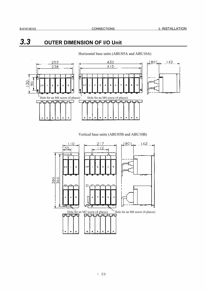
3.3 OUTER DIMENSION OF I/O Unit
Horizontal base units (ABU05A and ABU10A)
Vertical base units (ABU05B and ABU10B)
Hole for an M2 screw (4 places) Hole for an M4 screw (4 places)
Hole for an M4 screw (4 places) Hole for an M4 screw (4 places)

3. INSTALLATION CONNECTIONS B-61813E/03
-12-
Table 3.3 Heat value of each module
Module name Basic heatvalue (W)
Heat value per1 I/O point (W)
AIF01A 1.2 -AIF01B 1.2 -
*1 AID32A1 1.2 0.23*2 AID32B1 1.2 0.23
AID32H1 1.2 0.23AID16C 0.1 0.21AID16K 0.1 0.21AID16D 0.1 0.21AID16L 0.1 0.21
*3 AID32E1 0.1 0.23AID32E2 0.1 0.23
*4 AID32F1 0.1 0.23AID32F2 0.1 0.23AIA16G 0.1 0.21
*5 AOD32A1 0.3 -AOD08C 0.1 0.04+0.4×IL2
AOD08D 0.1 0.04+0.6×IL2
AOD16C 0.1 0.04+1.4×IL2
AOD16D 0.1 0.04+1.4×IL2
*6 AOD32C1 0.1 0.01+0.8×IL2
AOD32C2 0.1 0.01+0.8×IL2
*7 AOD32D1 0.1 0.01+0.8×IL2
AOD32D2 0.1 0.01+0.8×IL2
AOA05E 0.1 0.13+1.5×ILAOA08E 0.1 0.13+1.5×ILAOA12F 0.1 0.11+1.5×ILAOR08G 0.1 0.3+0.1×IL2
AOR16G 0.1 0.3+0.1×IL2
AOR16H2 0.1 0.3+0.1×IL2
AAD04A 3.1 -ADA02A 3.1 -ADA02B 3.1 -ACT01A 4.1 -ATI04A 4.0 -ATI04B 4.0 -
• Total `Heat value per 1 I/O point' for simultaneous ON points plus`Basic heat value' is the heat value of the module.
• IL : Load current of output
• A D32 1 of “*1 to *7" is the same module as formerA D32 .(Example : AID32E1 is equal to former AID32E.)

B-61813E/03 CONNECTIONS 3. INSTALLATION
-13-
3.4 MOUNTING AND DISMOUNTING MODULES
Interface modules and various types of I/O modules can be mounted toand dismounted from the base unit easily as shown below.
MountingHang the hook at the top of the module on the groove in the upperside of the base unit, and make the connector of the moduleengage with that of the base unit. Push the module in the lowergroove of the base unit till the stopper in the lower side of themodule stops.
DismountingRelease the stopper by pushing the lever at the bottom of themodule, and then push the module upwards.

4. CONNECTION CONNECTIONS B-61813E/03
-14-
4 CONNECTION
4.1 GENERAL CONNECTION DIAGRAM
NOTE1 Number of I/O Units and connecting method are
restricted depending on the allocation of the I/Opoints. Refer to the section 1.2,"Allocation of I/Opoints."
2 The number of I/O units per group is limited to 2 whenthe master equipment is the CNC.
3 Cable K1X can be an optical fiber cable by using theoptical I/O link adapter.
See chapter 10.4 Terminator TX is required for connector JD2 of the
AIF01B that is the last unit to be connected in thegroup. The terminator is not required when theAIF01B is not used.

B-61813E/03 CONNECTIONS 4. CONNECTION
-15-
4.2 CONNECTING INPUT POWER SOURCE
Connect the following power source with the connector CP32 of theinterface module (AIF01A, AIF01B, or AIF02C).• Voltage: 24VDC ±10%• Current: Determine from Table 4.4
AIF01A / AIF01B/AIF02CCP32
NOTETurn ON the power for the I/O unit just when or beforethe power for the CNC or the cell controller is turnedON. When the CNC or cell controller power is turnedOFF,make sure to turn the power to the I/O unit OFFas well. If the power is not turned on and offaccording to the above procedure, an error occurs inthe CNC or the controller, or the I/O unit is notnormally connected to the power.
t > 500 ms (Turn ON of the power for I/O unit can be late 500 ms or less.)
1 +24V
2 GND
3
Power for the master device
Power for the I/O unit
24VDC
BURNDY JAPAN Tripolur connector (Brown) Hoursing : SMS3PNS-5 A63L-0001-0202#3HN Contact : RC16M-SCT3 A63L-0001-0226

4. CONNECTION CONNECTIONS B-61813E/03
-16-
4.3 GROUNDING
Connect the grounding terminal of the base unit (ABU05A, ABU05B,ABU10A, or ABU10B) to ground.
(1) Horizontal type base unit
Use a wire of 2 mm2 or more for grounding.
(2) Vertical type base unit(a) For metal case
NOTEConnect the grounding terminal to the grounding holeportion.
(b) For plastic case
(2) When the cable K1X ( See overall connection figure in section4.1) runs between different cabinets, make sure to connect thecabinets with a wire more than 5.5 mm2.
Grounding terminal(M3 screw terminal)
M4 hole for gronding
Grounding terminal(M3 screw terminal)

B-61813E/03 CONNECTIONS 4. CONNECTION
-17-
4.4 REQUIRED CURRENT
Table 4.4 Required current of each module
Required current (mA) of+24VModule nameA B
AIF01A 50AIF01B 50AIF0K 50AID32A1 20+0.5×n 3.0+7.5×nAID32B1 20+0.5×n 3.0+7.5×nAID32H1 20+0.5×n 3.0+7.5×nAID16C 5AID16K 5AID16D 5AID16L 5AID32E1 5AID32E2 5AID32F1 5AID32F2 5AIA16G 5+1.5×nAOD32A1 14AOD08C 5+2×nAOD08D 5+2×nAOD16C 5+2×nAOD16D 5+2×nAOD32C1 5+0.5×nAOD32C2 5+0.5×nAOD32D1 5+0.5×nAOD32D2 5+0.5×nAOA05E 5+5.5×nAOA08E 5+5.5×nAOA12F 5+4.5×nAOR08G 5 10×nAOR16G 5 10×nAOR16H2 5 10×nAAD04A 5 130ADA02A 6 120ADA04B 5 130ACT01A 170+0.3×αATI04A 62.5 100ATI04B 62.5 100
n: Number of the input and output points (for each module)which turn ON simultaneously
α: +5-V current (mA) output to the outside
• Add the sums of the columns A and B for the modules to be used.The sum is the required current.(Unit:mA)
• For each base unit, keep the sum of column A and the sum ofcolumn B to within 500 mA and 1,500 mA, respectively.
4. CONNECTION CONNECTIONS B-61813E/03
-18-
4.5 INTERFACE MODULE (AIF01A, AIF01B)
Details of the cables K1X,K2X and the terminator shown in the generalconnection diagram are as follows.
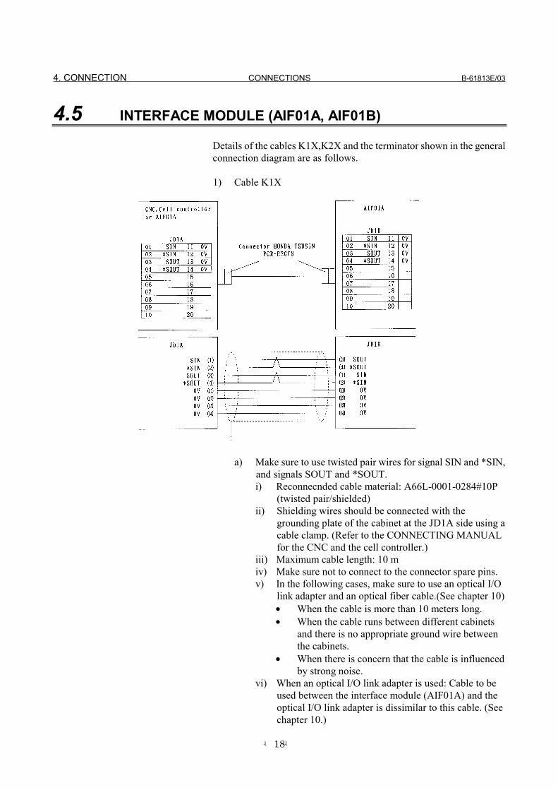
1) Cable K1X
a) Make sure to use twisted pair wires for signal SIN and *SIN,and signals SOUT and *SOUT.i) Reconnecnded cable material: A66L-0001-0284#10P
(twisted pair/shielded)ii) Shielding wires should be connected with the
grounding plate of the cabinet at the JD1A side using acable clamp. (Refer to the CONNECTING MANUALfor the CNC and the cell controller.)
iii) Maximum cable length: 10 miv) Make sure not to connect to the connector spare pins.v) In the following cases, make sure to use an optical I/O
link adapter and an optical fiber cable.(See chapter 10)• When the cable is more than 10 meters long.• When the cable runs between different cabinets
and there is no appropriate ground wire betweenthe cabinets.
• When there is concern that the cable is influencedby strong noise.
vi) When an optical I/O link adapter is used: Cable to beused between the interface module (AIF01A) and theoptical I/O link adapter is dissimilar to this cable. (Seechapter 10.)

B-61813E/03 CONNECTIONS 4. CONNECTION
-19-
2) Cable K2X
• Connect the signals with a same name.• Make sure to use twisted pair wires for the following signals:
S1 and * S1, S2 and *S2, S3 and *S3S4 and * S4, S5 and *S5, S6 and *S6
• Do not connect the pins No.10, No.19 and No.20 as they areused internally.
• Recommended cable material: A66L - 0001 - 0284#10P(twisted pair/shielded)
• Maximum cable length: 2m
AIF01BAIF01A or AIF01B

4. CONNECTION CONNECTIONS B-61813E/03
-20-
3) Terminator TX
• Terminate the connector JD2 of the last AIF01B in a singlegroup with the terminator. The connector need not beterminated when the AIF01B is not used.
• Short-circuit the TRM1s, the TRM2s and the TRM 3s oneanother respectively in a manner that a TRM1 is with anotherTRM1 and so on.
Short-circuit

B-61813E/03 CONNECTIONS 4. CONNECTION
-21-
4.6 INTERFACE MODULE (AIF02C) CONNECTION
4.6.1 Overview
One interface module (AIF02C) can control communication with bothI/O Unit-A and Unit-B, when it is connected to the FANUC I/O Link.
The following examples show a configuration in which twoconventional separate interface modules, I/O Unit-A and I/O Unit-B,are used and a configuration in which the AIF02C is used.
CNC cell controller
G roup #0
Group #1
Base expansion
(NOTE 2)
To the next group DI/DO unit DI/DO unit DI/DO unit DI/DO unit
CNC cell controller
(NOTE 2)
DI/DO unitTo the next group
Group #0
Group #1
(NOTE 1)
Base expansion
DI/DO unit DI/DO unit DI/DO unit
(1) Configuration example in which separate interface modulesare used
(2) Configuration example in which AIF02C is used

4. CONNECTION CONNECTIONS B-61813E/03
-22-
In this way, using the AIF02C eliminates the necessity for the interfaceunit (BIF04A1) for I/O Unit-B, which has conventionally been usedseparately; this configuration is suitable for a small I/O Unit-B system.Note the following points.
NOTES1 The AIF02C cannot be used for base expansion.2 The BIF04A1 can branch to a maximum of eight
communication lines.The AIF02C can branch only to a maximum of twodistributed link cables.
4.6.2 Connection
(1) Connection diagram[a] Configuration with two distributed link cables (note the
setting of the terminating resistor.)
CAUTIONS1 Set the terminating resistor DIP switch to ON2 Set the terminating resistor DIP switch to OFF.
[b] Connection with one Distributed Link cable (note the settingof the terminating resistor.)(From group n-1)
Groups nand n+1
(To group n+2)
Distributed link
DI/DO unit DI/DO unit DI/DO unit
DI/DO unit
(From group n-1)
Groups nand n+1
DI/DO unit DI/DO unit
DI/DO unitDI/DO unitDI/DO unit
(To group n+2)
Distributed link
B-61813E/03 CONNECTIONS 4. CONNECTION
-23-
CAUTIONS1 Set the terminating resistor DIP switch to ON.2 Set the terminating resistor DIP switch to OFF.
(2) Connection with the I/O linkThe AIF02C occupies two groups on the I/O link.When groups #n and #n+1 are used, for example, the smaller-numbered group, #n, is assigned to the I/O Unit-A, and thelarger-numbered group, #n+1, is assigned to the I/O Unit-B.[a] Connection of the I/O link cable
Connect the I/O link cable from the previous group to JD1B.Connect JD1A to the I/O link cable leading to the next group.Use the K1X I/O link signal cable, the same I/O link signalcable type as that for the AIF01A.
[b] Number of occupied I/O points on the I/O linkThe nominal number of occupied I/O points may differ fromthe actual number of I/O points. For the details of thenumber of I/O points occupied by the I/O Unit-B, refer toSection 4.2.1, "Number of points occupied on the interfaceunit I/O link," of the FANUC I/O Unit-B MODELConnection Manual (B-62163E).
(3) Connection with the distributed link (I/O Unit-B)[a] Number of distributed communication lines (I/O Unit-B)
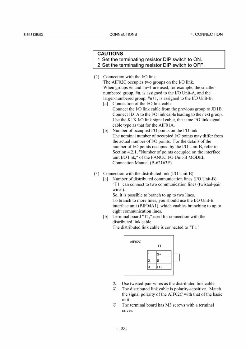
"T1" can connect to two communication lines (twisted-pairwires).So, it is possible to branch to up to two lines.To branch to more lines, you should use the I/O Unit-Binterface unit (BIF04A1), which enables branching to up toeight communication lines.
[b] Terminal board "T1," used for connection with thedistributed link cableThe distributed link cable is connected to "T1."
AIF02CT1
Use twisted-pair wires as the distributed link cable. The distributed link cable is polarity-sensitive. Match
the signal polarity of the AIF02C with that of the basicunit.
The terminal board has M3 screws with a terminalcover.
1 S+
2 S-
3 FG

4. CONNECTION CONNECTIONS B-61813E/03
-24-
Refer to Section 4.3, "Connecting a Distributed Link," and Section4.5.2, "Connecting the communications cable," of the FANUC I/OUnit-MODEL B Connection Manual (B-62163E) for details.
4.6.3 Setting with the DIP switch
In the AIF02C, distributed link settings can be made with the DIPswitch on the back of the module.The settings and corresponding signals are shown below.
12 Unused
34 EDSP5 Q6 H7 URDY8 R
(1) EDSP (error display method selection)Normally, set EDSP to the ON position.
(2) Q and H (communication speed setting)Normally, set both Q and H to the OFF positions.
(3) URDY (setting of the power on/off information for the unit)Normally, set URDY to the OFF position.
(4) R (terminating resistor setting)The ON position means that a terminating resistor must beinstalled. The OFF position means that no terminating resistorneed be installed.When only one communication cable is connected to the AIF02C,terminate it and the basic unit at the end of the communicationcable with a resistor.When two communication cables are connected to the AIF02C,terminate the basic unit connected to the end of eachcommunication cable with a resistor. Do not connect aterminating resistor to the AIF02C. (Refer to Section 4.6.2,"Connection.")
Refer to Section 5.1.1, "DIP switch setting," of the FANUC I/O Unit-MODEL B Connection Manual (B-62163E).

B-61813E/03 CONNECTIONS 4. CONNECTION
-25-
4.7 CONNECTING WITH I/O MODULES
From the point of view of an external connecting method, there are twotypes of I/O modules such as one with a terminal block and one with aconnector.
1) Connect with each module following the connection diagrams ofsections 4.2 and 5.3.
2) The terminal block is a removable type.
[Dismounting the terminal block] Open the cover of the terminal
block. Push up the latch at the top of the
terminal block. Drag out the tab at the top of the
terminal block and pull it out.The terminal block will beremoved from the module.
[Mounting the terminal block] Insert the protruding portion at
the bottom of the terminal blockin the groove of the moduleside.
Push the terminal block usingthe engaging point of the protruding portion and the grooveas an axis and mount it in the module firmly.
Open the cover of the terminal block and check to makesure the latch at the top of the terminal block is firmly set.
orHIROSEHIF3BB-50PA-2.54DS

4. CONNECTION CONNECTIONS B-61813E/03
-26-
3) Cautionary points when wiring terminal block type
• Wiring material : AWG22 to 18 (0.3 to 0.75 mm2)A wire as this as possible is recommended.
• Crimp style terminal : M3.5Crimp style terminal with noinsulation sleeve and a short distance"A", as illustrated in the drawingbelow, is recommended.
DAIDO TANSHI 1.25-S3.5NICHIFU TANSHI 1.25-3.5S etc.
• Mark tube : Use a short mark tube as possible and covercrimped part with the mark tube.

B-61813E/03 CONNECTIONS 5. DIGITAL INPUT/OUTPUT MODULES
-27-
5 DIGITAL INPUT/OUTPUT MODULES
5.1 LIST OF MODULES
Digital input modules
Input type modulename
Ratedvoltage
Ratedcurrent
Polarity Responsetime
Points Externalconnection
LEDdisplay
AID32A1 24VDC 7.5 mA Both Maximum20 ms
32 Connector A notprovided
AID32B1 24VDC 7.5 mA Both Maximum2 ms
32 Connector A notprovided
Non-insulationtype DCinput
AID32H1 24VDC 7.5 mA Both Maximum2 msMaximum20 ms
8
24
Connector A notprovided
AID16C 24VDC 7.5 mA NEG Maximum20 ms
16 Terminalblock
provided
AID16K 24VDC 7.5 mA NEG Maximum2 ms
16 Terminalblock
provided
AID16D 24VDC 7.5 mA POS Maximum20 ms
16 Terminalblock
provided
AID16L 24VDC 7.5 mA POS Maximum2 ms
16 Terminalblock
provided
AID32E1 24VDC 7.5 mA Both Maximum20 ms
32 Connector A notprovided
AID32E2 24VDC 7.5 mA Both Maximum20 ms
32 Connector B notprovided
AID32F1 24VDC 7.5 mA Both Maximum2 ms
32 Connector A notprovided
Insulationtype DCinput
AID32F2 24VDC 7.5 mA Both Maximum2 ms
32 Connector B notprovided
AC input AIA16G 100 to120VAC
10.5 mA(120VAC)
ON Max 35msOFF Max 45ms
16 Terminalblock
provided
NOTE1 Polarity
Negative : 0 V common (current source type) Regardto be ON when input is at Low level.
Positive : 24 V common (current sink type) Regard tobe ON when input is High level.
2 Connector A : HONDA MR ConnectorConnector B : Flat Cable Connector
3 For the details of the specifications for each module,refer to the section 5.3.

5. DIGITAL INPUT/OUTPUT MODULES CONNECTIONS B-61813E/03
-28-
Digital output modules
Outputtype
Modulename
Ratedvoltage
Maximumcurrent
Polarity Points Points/common
Externaconnection
LED display
Fuse
Non-insulationtype DCoutput
AOD32A1 5 to 24VDC 0.3A NEG 32 8 Connector A not provided
not provided
AOD08C 2A NEG 8 8 Terminalblock
provided provided
AOD08D 2A POS 8 8 Terminalblock
provided provided
AOD16C 0.5A NEG 16 8 Terminalblock
provided notprovided
AOD16D 0.5A POS 16 8 Terminalblock
provided notprovided
AOD32C1 0.3A NEG 32 8 Connector A notprovided
notprovided
AOD32C2 0.3A NEG 32 8 Connector B notprovided
notprovided
AOD32D1 0.3A POS 32 8 Connector A notprovided
notprovided
InsulationtypeDC output
AOD32D2
12 to 24VDC
0.3A POS 32 8 Connector B notprovided
notprovided
AOA05E 2A - 5 1 Terminalblock
provided provided
AOA08E
100 to240VAC
1A - 8 4 Terminalblock
provided provided
AC output
AOA12F 100 to120VAC
0.5A - 12 6 Terminalblock
provided provided
AOR08G 4A - 8 1 Terminalblock
provided notprovided
AOR16G
Maximum250VAC/30VDC 2A - 16 4 Terminal
blockprovided not
provided
RELAYoutput
AOR16H2 30VDC 2A - 16 4 Connector B provided notprovided
NOTE1 Polarity
Negative : 0 V common (current sink type) Output is atLow level when ON.
Positive : 24 V common (current source type) Outputis at High level when ON.
2 Connector A : HONDA MR ConnectorConnector B : Flat Cable Connector
3 For the details of the specifications for each module,refer to the section 5.3.
4 The maximum current of the DC output moduleincludes the permissible rush current.

B-61813E/03 CONNECTIONS 5. DIGITAL INPUT/OUTPUT MODULES
-29-
5.2 CORRESPONDENCE BETWEEN I/O SIGNALS ANDADDRESSES IN A MODULE
Addresses in a module are addresses defined for each module. Theyare relative addresses in a module with the beginning address in themodule as 0. Real addresses viewed from the sequence program of thePMC are set by the programmer.
For input modules, an input signal becomes "1" when the contact pointconnected with the input is turned ON. On the other hand, for outputmodules, an output contact point (or transistor) is turned ON when theoutput signal is "1."

5. DIGITAL INPUT/OUTPUT MODULES CONNECTIONS B-61813E/03
-30-
5.3 SPECIFICATION FOR EACH MODULE
Specifications for each I/O module are shown in the following pages.
(1) Input module AID32A1(2) Input module AID32B1(3) Input module AID32H1(4) Input module AID16C(5) Input module AID16K(6) Input module AID16D(7) Input module AID16L(8) Input module AID32E1(9) Input module AID32E2(10) Input module AID32F1(11) Input module AID32F2(12) Input module AIA16G(13) Output module AOD32A1(14) Output module AOD08C(15) Output module AOD08D(16) Output module AOD16C(17) Output module AOD16D(18) Output module AOD32C1(19) Output module AOD32C2(20) Output module AOD32D1(21) Output module AOD32D2(22) Output module AOA05E(23) Output module AOA08E(24) Output module AOA12F(25) Output module AOR08G(26) Output module AOR16G(27) Output module AOR16H2

B-61813E/03 CONNECTIONS 5. DIGITAL INPUT/OUTPUT MODULES
-31-
(1) Input module AID32A1 (Non-insulation type)
Item SpecificationsPoints/module 32 pointsPoints/common 16 points/commonSink/source current Both directionsInput voltage 24VDC +10%, −20%Input current 7.5mA (average)ON voltage, current Min. 18VDC, min. 6mAOFF voltage, current Max. 6VDC, max. 1.5mA
OFF→ON Max.20msResponsetime
ON→OFF Max.20ms
This is the value from input to output in the module. The actual value isdetermined by adding it to the scanning time depending on eachsystem.
Input display Not providedExternal connection Connector (HONDA TSUSIN MR-50RMA)Terminal connection andcircuitry
+24V or GND can be selected for input common as above fig.
NOTE1 Make sure to connect all common (CMA, CMC) pins.2 This module outputs +24 V on pins 13, 17, 04, and 08.

5. DIGITAL INPUT/OUTPUT MODULES CONNECTIONS B-61813E/03
-32-
(2) Input module AID32B1 (Non-insulation type)
Item SpecificationsPoints/module 32 pointsPoints/common 16 points/commonSink/source current Both directionsInput voltage 24VDC +10%, −20%Input current 7.5mA (average)ON voltage, current Min. 18VDC, min. 6mAOFF voltage, current Max. 6VDC, max. 1.5mA
OFF→ON Max.2msResponsetime
ON→OFF Max.2ms
This is the value from input to output in the module. The actual value isdetermined by adding it to the scanning time depending on eachsystem.
Input display Not providedExternal connection Connector (HONDA TSUSIN MR-50RMA)Terminal connection andcircuitry
+24V or GND can be selected for input common as above fig.
NOTE1 Make sure to connect all common (CMA, CMC) pins.2 This module outputs +24 V on pins 13, 17, 04, and 08.

B-61813E/03 CONNECTIONS 5. DIGITAL INPUT/OUTPUT MODULES
-33-
(3) Input module AID32H1
Item SpecificationsPoints/module 32 pointsPoints/common 16 points/commonSink/source current Both directionsInput voltage 24VDC +10%, −20%Input current 7.5mA (average)ON voltage, current Min. 18VDC, min. 6mAOFF voltage, current Max. 6VDC, max. 1.5mA
OFF→ON Max.2ms(A0 to A7)Max.20ms(B0 to D7)
Responsetime
ON→OFF Max.2ms(A0 to A7)Max.20ms(B0 to D7)
This is the value from input to output in the module. The actual value isdetermined by adding it to the scanning time depending on eachsystem.
Input display Not providedExternal connection Connector (HONDA TSUSIN MR-50RMA)Terminal connection andcircuitry
+24V or GND can be selected for input common as above fig.
NOTE1 Make sure to connect all common (CMA, CMC) pins.2 This module outputs +24 V on pins 13, 17, 04, and 08.
5. DIGITAL INPUT/OUTPUT MODULES CONNECTIONS B-61813E/03
-34-
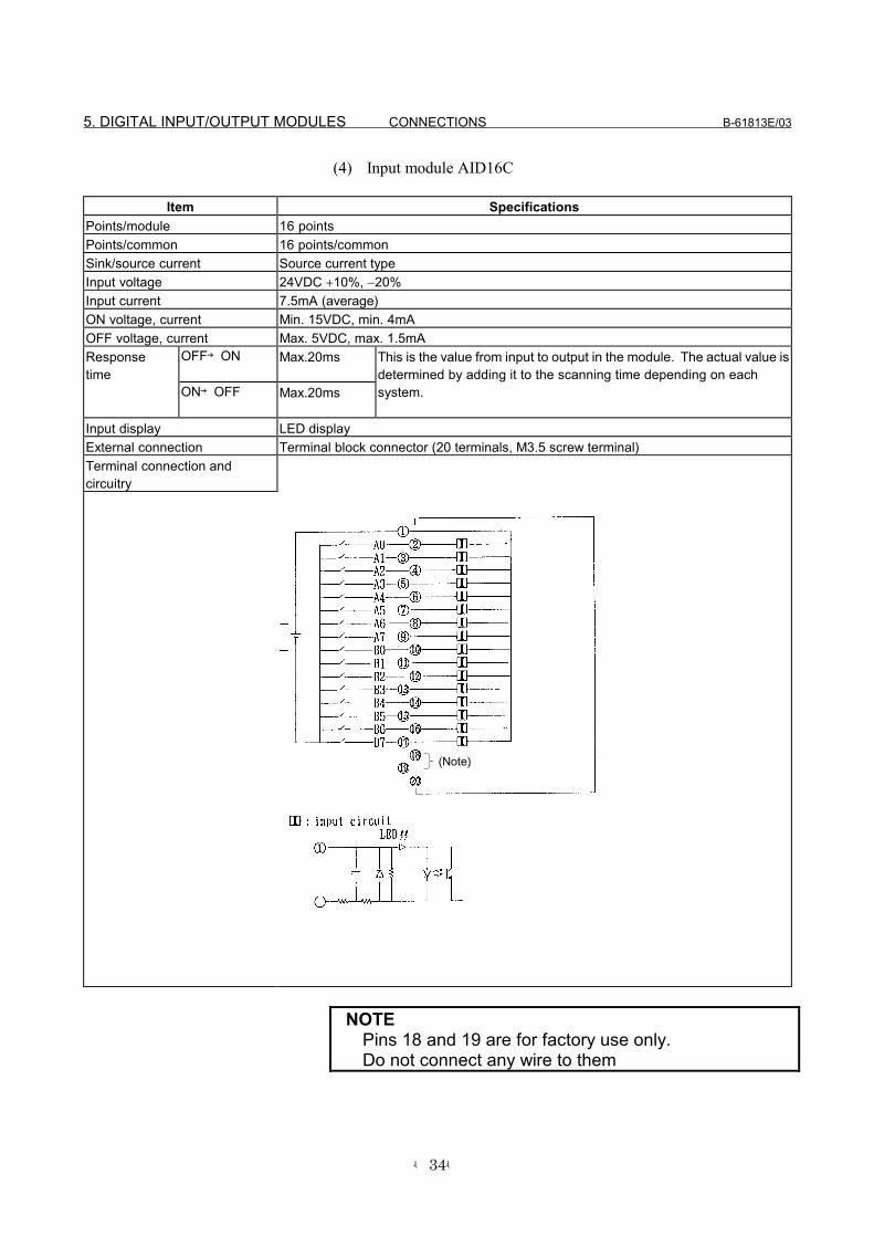
(4) Input module AID16C
Item SpecificationsPoints/module 16 pointsPoints/common 16 points/commonSink/source current Source current typeInput voltage 24VDC +10%, −20%Input current 7.5mA (average)ON voltage, current Min. 15VDC, min. 4mAOFF voltage, current Max. 5VDC, max. 1.5mA
OFF→ON Max.20msResponsetime
ON→OFF Max.20ms
This is the value from input to output in the module. The actual value isdetermined by adding it to the scanning time depending on eachsystem.
Input display LED displayExternal connection Terminal block connector (20 terminals, M3.5 screw terminal)Terminal connection andcircuitry
NOTEPins 18 and 19 are for factory use only.Do not connect any wire to them
(Note)

B-61813E/03 CONNECTIONS 5. DIGITAL INPUT/OUTPUT MODULES
-35-
(5) Input module AID16K
Item SpecificationsPoints/module 16 pointsPoints/common 16 points/commonSink/source current Source current typeInput voltage 24VDC +10%, −20%Input current 7.5mA (average)ON voltage, current Min. 15VDC, min. 4mAOFF voltage, current Max. 5VDC, max. 1.5mA
OFF→ON Max.2msResponsetime
ON→OFF Max.2ms
This is the value from input to output in the module. The actual value isdetermined by adding it to the scanning time depending on eachsystem.
Input display LED displayExternal connection Terminal block connector (20 terminals, M3.5 screw terminal)Terminal connection andcircuitry
NOTEPins 18 and 19 are for factory use only.Do not connect any wire to them
(Note)

5. DIGITAL INPUT/OUTPUT MODULES CONNECTIONS B-61813E/03
-36-
(6) Input module AID16D
Item SpecificationsPoints/module 32 pointsPoints/common 16 points/commonSink/source current Sink current typeInput voltage 24VDC +10%, −20%Input current 7.5mA (average)ON voltage, current Min. 15VDC, min. 4mAOFF voltage, current Max. 5VDC, max. 1.5mA
OFF→ON Max.20msResponsetime
ON→OFF Max.20ms
This is the value from input to output in the module. The actual value isdetermined by adding it to the scanning time depending on eachsystem.
Input display LED displayExternal connection Terminal block connector (20 terminals, M3.5 screw terminal)Terminal connection andcircuitry
NOTEPins 18 and 19 are for factory use only.Do not connect any wire to them
(Note)

B-61813E/03 CONNECTIONS 5. DIGITAL INPUT/OUTPUT MODULES
-37-
(7) Input module AID16L
Item SpecificationsPoints/module 16 pointsPoints/common 16 points/commonSink/source current Source current typeInput voltage 24VDC +10%, −20%Input current 7.5mA (average)ON voltage, current Min. 15VDC, min. 4mAOFF voltage, current Max. 5VDC, max. 1.5mA
OFF→ON Max.2msResponsetime
ON→OFF Max.2ms
This is the value from input to output in the module. The actual value isdetermined by adding it to the scanning time depending on eachsystem.
Input display LED displayExternal connection Terminal block connector (20 terminals, M3.5 screw terminal)Terminal connectionand circuitry
NOTEPins 18 and 19 are for factory use only.Do not connect any wire to them
(Note)

5. DIGITAL INPUT/OUTPUT MODULES CONNECTIONS B-61813E/03
-38-
(8) Input module AID32E1
Item SpecificationsPoints/module 32 pointsPoints/common 8 points/commonSink/source current Both directionsInput voltage 24VDC +10%, −20%Input current 7.5mA (average)ON voltage, current Min. 15VDC, min. 4.5mAOFF voltage, current Max. 6VDC, max. 2mA
OFF→ON Max.20msResponsetime
ON→OFF Max.20ms
This is the value from input to output in the module. The actual value isdetermined by adding it to the scanning time depending on eachsystem.
Input display Not providedExternal connection Connector (HONDA TSUSIN MR-50RMA)Terminal connection andcircuitry

B-61813E/03 CONNECTIONS 5. DIGITAL INPUT/OUTPUT MODULES
-39-
(9) Input module AID32E2
Item SpecificationsPoints/module 32 pointsPoints/common 8 points/commonSink/source current Both directionsInput voltage 24VDC +10%, −20%Input current 7.5mA (average)ON voltage, current Min. 15VDC, min. 4.5mAOFF voltage, current Max. 6VDC, max. 2mA
OFF→ON Max.20msResponsetime
ON→OFF Max.20ms
This is the value from input to output in the module. The actual value isdetermined by adding it to the scanning time depending on eachsystem.
Input display Not providedExternal connection Connector (HIROSE ELECTRIC HIF3BB-50PA-2.54DS in accordance with MIL
standard)Terminal connection andcircuitry
5. DIGITAL INPUT/OUTPUT MODULES CONNECTIONS B-61813E/03
-40-
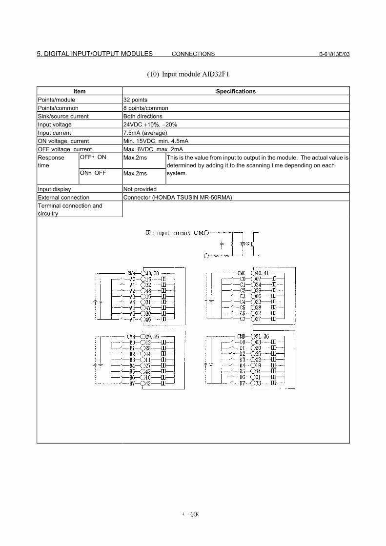
(10) Input module AID32F1
Item SpecificationsPoints/module 32 pointsPoints/common 8 points/commonSink/source current Both directionsInput voltage 24VDC +10%, −20%Input current 7.5mA (average)ON voltage, current Min. 15VDC, min. 4.5mAOFF voltage, current Max. 6VDC, max. 2mA
OFF→ON Max.2msResponsetime
ON→OFF Max.2ms
This is the value from input to output in the module. The actual value isdetermined by adding it to the scanning time depending on eachsystem.
Input display Not providedExternal connection Connector (HONDA TSUSIN MR-50RMA)Terminal connection andcircuitry

B-61813E/03 CONNECTIONS 5. DIGITAL INPUT/OUTPUT MODULES
-41-
(11) Input module AID32F2
Item SpecificationsPoints/module 32 pointsPoints/common 8 points/commonSink/source current Both directionsInput voltage 24VDC +10%, −20%Input current 7.5mA (average)ON voltage, current Min. 15VDC, min. 4.5mAOFF voltage, current Max. 6VDC, max. 2mA
OFF→ON Max.2msResponsetime
ON→OFF Max.2ms
This is the value from input to output in the module. The actual value isdetermined by adding it to the scanning time depending on eachsystem.
Input display Not providedExternal connection Connector (HIROSE ELECTRIC HIF3BB-50PA-2.54DS in accordance with MIL
standard)Terminal connection andcircuitry

5. DIGITAL INPUT/OUTPUT MODULES CONNECTIONS B-61813E/03
-42-
(12) Input module AIA16G
Item SpecificationsPoints/module 16 pointsPoints/common 16 points/commonSink/source current 100 to 115VAC ±15%Input voltage 132Vrms, 50/60 HzInput current 10.55mArms (120VAC, 50Hz)ON voltage, current Min. 74Vrms, min. 6mArmsOFF voltage, current Max. 20Vrms, max. 2.2mArms
OFF→ON Max.35msResponsetime
ON→OFF Max.45ms
This is the value from input to output in the module. The actual value isdetermined by adding it to the scanning time depending on eachsystem.
Input display LED displayExternal connection Terminal block connector (20 terminals, M3.5 screw terminal)Common 16 points/commonTerminal connection andcircuitry

B-61813E/03 CONNECTIONS 5. DIGITAL INPUT/OUTPUT MODULES
-43-
(13) Output module AOD32A1 (Non-insulation type)
Item SpecificationsPoints/module 32 pointsPoints/common 8 points/commonSink/source current Sink current typeRated load voltage 5 to 24VDC +20%, −15%Maximum load current 0.3A (however 2A/common)Maximum voltage drop when ON 0.24V (load current ×0.8Ω)Maximum leak current whenOFF
0.1mA
OFF→ON Max.1msResponsetime ON→OFF Max.1msInput display Not providedExternal connection Connector (HONDA TSUSIN MR-50RMA)Terminal connection andcircuitry
NOTEFor the common (CMA, CMB, CMC, CMD) , makesure to use both of them.
to

5. DIGITAL INPUT/OUTPUT MODULES CONNECTIONS B-61813E/03
-44-
(14) Output module AOD08C
Item SpecificationsPoints/module 8 pointsPoints/common 8 points/commonSink/source current Sink current typeRated load voltage 12 to 24VDC +20%, −15%Maximum load current 2A (however 4A/fuse)Maximum voltage drop when ON 0.8V (load current ×0.4Ω)Maximum leak current whenOFF
0.1mA
OFF→ON Max.2msResponsetime
ON→OFF Max.2ms
This is the value from input to output in the module. The actual value isdetermined by adding it to the scanning time depending on eachsystem.
Input display LED displayExternal connection Terminal block connector (20 terminals, M3.5 screw terminal)Fuse 5A, 1 piece for each output A0-A3 and A4-A7.Terminal connection andcircuitry

B-61813E/03 CONNECTIONS 5. DIGITAL INPUT/OUTPUT MODULES
-45-
(15) Output module AOD08D
Item SpecificationsPoints/module 8 pointsPoints/common 8 points/commonSink/source current Source current typeRated load voltage 12 to 24VDC +20%, −15%Maximum load current 2A (however 4A/fuse)Limit of load Refer to load derating curve (Fig. 5.3(a))Maximum voltage drop when ON 1.2V (load current ×0.6Ω)Maximum leak current whenOFF
0.1mA
OFF→ON Max.2msResponseTime
ON→OFF Max.2ms
This is the value from input to output in the module. The actual value isdetermined by adding it to the scanning time depending on eachsystem.
Output display LED displayExternal connection Terminal block connector (20 terminals, M3.5 screw terminal)Fuse 5A, 1 piece for each output A0-A3 and A4-A7.Terminal connection andcircuitry

5. DIGITAL INPUT/OUTPUT MODULES CONNECTIONS B-61813E/03
-46-
(16) Output module AOD16C
Item SpecificationsPoints/module 16 pointsPoints/common 8 points/commonSink/source current Sink current typeRated load voltage 12 to 24VDC +20%, −15%Maximum load current 0.5A (however 2A/common)Maximum voltage drop when ON 0.7V (load current ×1.4Ω)Maximum leak current whenOFF
0.1Ma
OFF→ON Max.2msResponsetime
ON→OFF Max.2ms
This is the value from input to output in the module. The actual value isdetermined by adding it to the scanning time depending on eachsystem.
Output display LED displayExternal connection Terminal block connector (20 terminals, M3.5 screw terminal)Terminal connection andcircuitry

B-61813E/03 CONNECTIONS 5. DIGITAL INPUT/OUTPUT MODULES
-47-
(17) Output module AOD16D
Item SpecificationsPoints/module 16 pointsPoints/common 8 points/commonSink/source current Source current typeRated load voltage 12 to 24VDC +20%, −15%Maximum load current 0.5A (however 2A/common)Maximum voltage drop when ON 0.7V (load current ×1.4Ω)Maximum leak current whenOFF
0.1mA
OFF→ON Max.2msResponsetime
ON→OFF Max.2ms
This is the value from input to output in the module. The actual value isdetermined by adding it to the scanning time depending on eachsystem.
Output display LED displayExternal connection Terminal block connector (20 terminals, M3.5 screw terminal)Terminal connection andcircuitry
5. DIGITAL INPUT/OUTPUT MODULES CONNECTIONS B-61813E/03
-48-
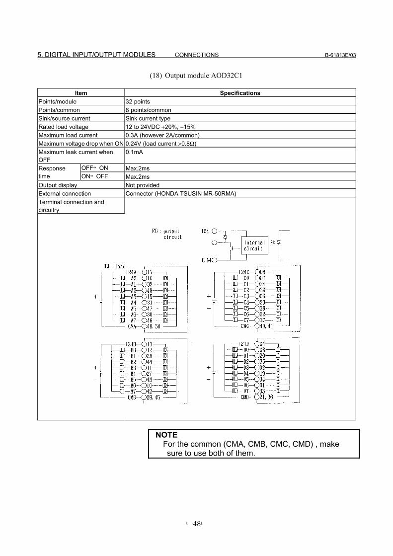
(18) Output module AOD32C1
Item SpecificationsPoints/module 32 pointsPoints/common 8 points/commonSink/source current Sink current typeRated load voltage 12 to 24VDC +20%, −15%Maximum load current 0.3A (however 2A/common)Maximum voltage drop when ON 0.24V (load current ×0.8Ω)Maximum leak current whenOFF
0.1mA
OFF→ON Max.2msResponsetime ON→OFF Max.2msOutput display Not providedExternal connection Connector (HONDA TSUSIN MR-50RMA)Terminal connection andcircuitry
NOTEFor the common (CMA, CMB, CMC, CMD) , makesure to use both of them.

B-61813E/03 CONNECTIONS 5. DIGITAL INPUT/OUTPUT MODULES
-49-
(19) Output module AOD32C2
Item SpecificationsPoints/module 32 pointsPoints/common 8 points/commonSink/source current Sink current typeRated load voltage 12 to 24VDC +20%, −15%Maximum load current 0.3A (however 2A/common)Maximum voltage drop when ON 0.24V (load current ×0.8Ω)Maximum leak current whenOFF
0.1mA
OFF→ON Max.2msResponsetime ON→OFF Max.2msOutput display Not providedExternal connection Connector (HIROSE ELECTRIC HIF3BB-50PA-2.54DS in accordance with MIL
standard)Terminal connection andcircuitry
NOTEFor the common (CMA, CMB, CMC, CMD), make sureto use both of them.

5. DIGITAL INPUT/OUTPUT MODULES CONNECTIONS B-61813E/03
-50-
(20) Output module AOD32D1
Item SpecificationsPoints/module 32 pointsPoints/common 8 points/commonSink/source current Source current typeRated load voltage 12 to 24VDC +20%, −15%Maximum load current 0.3A (however 2A/common)Maximum voltage drop when ON 0.24V (load current ×0.8Ω)Maximum leak current whenOFF
0.1mA
OFF→ON Max.2msResponseTime ON→OFF Max.2msOutput display Not providedExternal connection Connector (HONDA TSUSIN MR-50RMA)Terminal connection andcircuitry
NOTEFor the common (CMA, CMB, CMC, CMD), make sureto use both of them.

B-61813E/03 CONNECTIONS 5. DIGITAL INPUT/OUTPUT MODULES
-51-
(21) Output module AOD32D2
Item SpecificationsPoints/module 32 pointsPoints/common 8 points/commonSink/source current Source current typeRated load voltage 12 to 24VDC +20%, −15%Maximum load current 0.3A (however 2A/common)Maximum voltage drop when ON 0.24V (load current ×0.8Ω)Maximum leak current whenOFF
0.1mA
OFF→ON Max.2msResponsetime ON→OFF Max.2msOutput display Not providedExternal connection Connector (HIROSE ELECTRIC HIF3BB-50PA-2.54DS in accordance with MIL
standard)Terminal connection andcircuitry
NOTEFor the common (CMA, CMB, CMC, CMD), make sureto use both of them.

5. DIGITAL INPUT/OUTPUT MODULES CONNECTIONS B-61813E/03
-52-
(22) Output module AOA05E
Item SpecificationsPoints/module 5 pointsPoints/common 1 points/commonRated load voltage 100 to 230VAC ±15%, 47 to 63HzMaximum load current 2A/point (howerver 5A/module)Maximum rush current 25A ( 1 period)Limit of load Refer to load derating curve (Fig. 5.3 (b))Maximum voltage drop when ON 1.5VrmsMaximum leak current whenOFF
3.0mA (115VAC), 6.0mA (230VAC)
OFF→ON Max.1msResponsetime
ON→OFF Half of the loadferquency orless
This is the value from input to output in the module. The actual value isdetermined by adding it to the scanning time depending on eachsystem.
Output display LED displayExternal connection Terminal block connector (20 terminals, M3.5 screw terminal)Fuse 3.2A, 1 piece for each output A0 to A4Terminal connection andcircuitry

B-61813E/03 CONNECTIONS 5. DIGITAL INPUT/OUTPUT MODULES
-53-
(23) Output module AOA08E
Item SpecificationsPoints/module 8 pointsPoints/common 4 points/commonRated load voltage 100 to 230VAC ±15%, 47 to 63HzMaximum load current 1A/point ( howerver 2A/common)Maximum in rush current 10A ( 1 period)Maximum voltage drop when ON 1.5VrmsMaximum leak current whenOFF
3.0mA (115VAC), 6.0mA (230VAC)
OFF→ON Max.1msResponsetime
ON→OFF Half of the loadferquency orless
This is the value from input to output in the module. The actual value isdetermined by adding it to the scanning time depending on eachsystem.
Output display LED displayExternal connection Terminal block connector (20 terminals, M3.5 screw terminal)Fuse 3.2A, 1 piece for each output A0 to A3 and A4 to A7Terminal connection andcircuitry

5. DIGITAL INPUT/OUTPUT MODULES CONNECTIONS B-61813E/03
-54-
(24) Output module AOA12F
Item SpecificationsPoints/module 12 pointsPoints/common 6 points/commonRated load voltage 100 to 115VAC ±15%, 47 to 63HzMaximum load current 0.5A/point ( howerver, 2A/common)Maximum in rush current 5A ( 1 period)Limit of load Refer to load derating curve (Fig. 5.3 (c))Maximum voltage drop when ON 1.5VrmsMaximum leak current whenOFF
1.5mA (115VAC)
OFF→ON Max.1msResponsetime
ON→OFF Half of the loadferquency orless
This is the value from input to output in the module. The actual value isdetermined by adding it to the scanning time depending on eachsystem.
Output display LED displayExternal connection Terminal block connector (20 terminals, M3.5 screw terminal)Fuse 3.2A, 1 piece for each output A0 to A5 and B0 to B5Terminal connection andcircuitry

B-61813E/03 CONNECTIONS 5. DIGITAL INPUT/OUTPUT MODULES
-55-
(25) Output module AOR08G
Item SpecificationsPoints/module 8 pointsPoints/common 1 points/commonMaximum load 30VDC/250VAC, 4A (resistance load)Minimum load 5VDC, 10mALimit of load Refer to load derating curve (Fig. 5.3 (d))Maximum voltage drop when ON 1.5VrmsMaximum leak current whenOFF
1.5mA (115VAC)
OFF→ON Max.15msResponsetime
ON→OFF Max.15ms
This is the value from input to output in the module. The actual value isdetermined by adding it to the scanning time depending on eachsystem.
Output display LED displayExternal connection Terminal block connector (20 terminals, M3.5 screw terminal)Fuse 3.2A, 1 piece for each output A0 to A5 and B0 to B5
Mechanical Min. 20,000,000 timesRelay lifeElectrical Min. 100,000 times (resistance load)
Terminal connection andcircuitry
V : Direct current power or alternating current power
5. DIGITAL INPUT/OUTPUT MODULES CONNECTIONS B-61813E/03
-56-
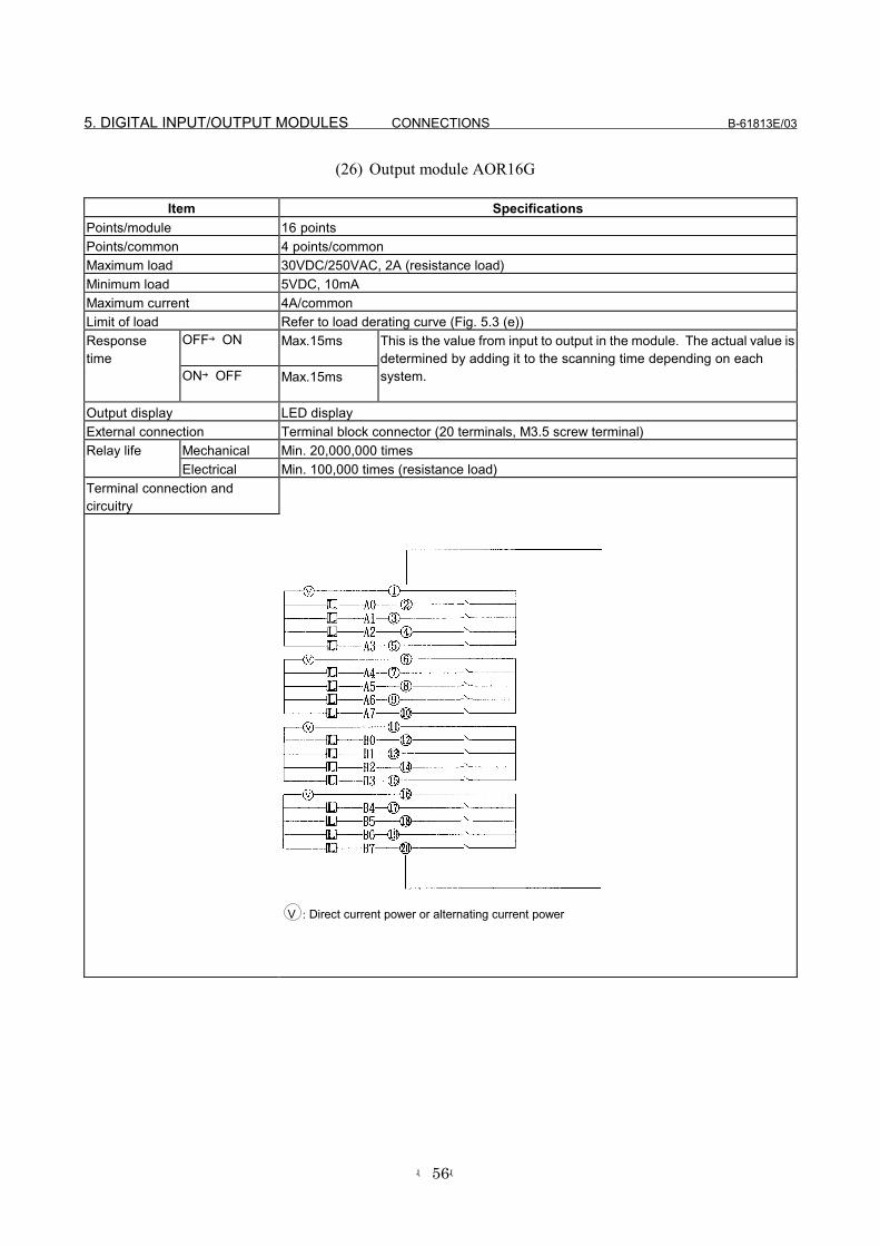
(26) Output module AOR16G
Item SpecificationsPoints/module 16 pointsPoints/common 4 points/commonMaximum load 30VDC/250VAC, 2A (resistance load)Minimum load 5VDC, 10mAMaximum current 4A/commonLimit of load Refer to load derating curve (Fig. 5.3 (e))
OFF→ON Max.15msResponsetime
ON→OFF Max.15ms
This is the value from input to output in the module. The actual value isdetermined by adding it to the scanning time depending on eachsystem.
Output display LED displayExternal connection Terminal block connector (20 terminals, M3.5 screw terminal)
Mechanical Min. 20,000,000 timesRelay lifeElectrical Min. 100,000 times (resistance load)
Terminal connection andcircuitry
V : Direct current power or alternating current power

B-61813E/03 CONNECTIONS 5. DIGITAL INPUT/OUTPUT MODULES
-57-
(27) Output module AOR16H2
Item SpecificationsPoints/module 16 pointsPoints/common 4 points/commonMaximum load 30VDC, 2A (resistance load)Minimum load 5VDC, 10mAMaximum current 4A/commonLimit of load Refer to load derating curve (Fig. 5.3 (e))
OFF→ON Max.15msResponsetime
ON→OFF Max.15ms
This is the value from input to output in the module. The actual value isdetermined by adding it to the scanning time depending on eachsystem.
Output display LED displayExternal connection Connector (HIROSE ELECTRIC HIF3BB-50PA-2.54DS in accordance with MIL
standard)Mechanical Min. 20,000,000 timesRelay lifeElectrical Min. 100,000 times (resistance load)
Terminal connection andcircuitry

5. DIGITAL INPUT/OUTPUT MODULES CONNECTIONS B-61813E/03
-58-
Fig.5.3 (a) AOD08D Load reduction curve
NOTEAmbient temperature means the temperaturesurrounding the I/O unit and not that surrounding thecabinet containing the I/O unit.
Fig.5.3 (b) AOA05E Load reduction curve

B-61813E/03 CONNECTIONS 5. DIGITAL INPUT/OUTPUT MODULES
-59-
Fig.5.3 (c) AOA12F Load reduction curve
NOTEAmbient temperature means the temperaturesurrounding the I/O unit and not that surrounding thecabinet containing the I/O unit.

5. DIGITAL INPUT/OUTPUT MODULES CONNECTIONS B-61813E/03
-60-
Fig.5.3 (d) AOR08G Load reduction curve
Fig.5.3 (e) AOR16G, AOR16H2 Load reduction curve
NOTEAmbient temperature means the temperaturesurrounding the I/O unit and not that surrounding thecabinet containing the I/O unit.

B-61813E/03 CONNECTIONS 6. ANALOG INPUT MODULE (AAD04A)
-61-
6 ANALOG INPUT MODULE (AAD04A)
6.1 SPECIFICATIONS FOR ANALOG INPUT MODULE
Item SpecificationsNumber of inputchannel
4 channel/module
Analog input -10VDC to+10VDC(input resistance 4.7MΩ)-20mADC to+20mADC(input resistance 250Ω)Selectable
Digital output 12 bit binary (complementary representation of "2".)Input/outputcorrespondence
Resolution 5mV or 20µATotal precision Voltage input ±0.5%(For full scale)
Current input ±1%(For full scale)Conversionary time Max.2ms(note)Maximum inputvoltage/current
±15V, ±30mA
Isolation Photocoupler isolated(between the input signal andthe base)However, not isolated between input channels
Output connecting Removable terminal block(20 terminals, M3.5 screwterminal)
Required inputpoints
64 points
NOTEConversion time means that only in a module. Actualresponse speed is ditermined by adding the scanningtime depending on each system to this conversiontime.
Analog input Digital output+10V +2000+5V or + 20mA +10000V or 0mA 0-5V or -20mA -1000-10V -2000

6. ANALOG INPUT MODULE (AAD04A) CONNECTIONS B-61813E/03
-62-
6.2 CORRESPONDENCE BETWEEN INPUT SIGNALS ANDADDRESSES IN A MODULE
In the analog input module AAD04A, the 4-channel analog inputsignals are cyclically A-D converted in order, and the converted digitaldata are written in the following addresses. Therefore, in the PMCprogram, it is possible at any time to know the values for the analoginput signals by referring to the following addresses.
(1) PMC-N, Q (PMC for Series 15 AND F-D Mate)
Addressin module 7 6 5 4 3 2 1 0
0 X-0 X-0 X-0 X-0 D11-0 D10-0 D09-0 D08-0
Channel 0
1 D07-0 D06-0 D05-0 D04-0 D03-0 D02-0 D01-0 D00-0
2 X-1 X-1 X-1 X-1 D11-1 D10-1 D09-1 D08-1
Channel 1
3 D07-1 D06-1 D05-1 D04-1 D03-1 D02-1 D01-1 D00-1
4 X-2 X-2 X-2 X-2 D11-2 D10-2 D09-2 D08-2
Channel 2
5 D07-2 D06-2 D05-2 D04-2 D03-2 D02-2 D01-2 D00-2
6 X-3 X-3 X-3 X-3 D11-3 D10-3 D09-3 D08-3
Channel 3
7 D07-3 D06-3 D05-3 D04-3 D03-3 D02-3 D01-3 D00-3
D00-n and D11-n correspond to the weights of 20 and 211 respectively.Here, D11-n corresponds to the sign bit in the complementaryrepresentation of "2."In addition, in X-n is written the same value as that in D11-n.
NOTEWhen addressing I/O modules, the beginning addressfor this module should be assigned to an even one.Moreover, when an A-D converted value is referredto in a PMC program, make sure to read the data inunit of a word (16 bits).
Bits

B-61813E/03 CONNECTIONS 6. ANALOG INPUT MODULE (AAD04A)
-63-
(2) PMC-M, R (PMC for Series 0, Series 16, Series 18)
Addressin module 7 6 5 4 3 2 1 0
0 D07-0 D06-0 D05-0 D04-0 D03-0 D02-0 D01-0 D00-0
Channel 0
1 X-0 X-0 X-0 X-0 D11-0 D10-0 D09-0 D08-0
2 D07-1 D06-1 D05-1 D04-1 D03-1 D02-1 D01-1 D00-1
Channel 1
3 X-1 X-1 X-1 X-1 D11-1 D10-1 D09-1 D08-1
4 D07-2 D06-2 D05-2 D04-2 D03-2 D02-2 D01-2 D00-2
Channel 2
5 X-2 X-2 X-2 X-2 D11-2 D10-2 D09-2 D08-2
6 D07-3 D06-3 D05-3 D04-3 D03-3 D02-3 D01-3 D00-3
Channel 3
7 X-3 X-3 X-3 X-3 D11-3 D10-3 D09-3 D08-3
D00-n and D11-n correspond to the weights of 20 and 211 respectively.Here, D11-n corresponds to the sign bit in the complementaryrepresentation of "2."In addition, in X-n is written the same value as that in D11-n.
NOTEWhen addressing I/O modules, the beginning addressfor this module should be assigned to an even one.Moreover, when an A-D converted value is referredto in a PMC program, make sure to read the data inunit of a word (16 bits).
Bits

6. ANALOG INPUT MODULE (AAD04A) CONNECTIONS B-61813E/03
-64-
6.3 CONNECTING WITH ANALOG INPUT MODULE
NOTE1 Though the example above shows the connection of
channels 0 and 2, it is just the same with the cahnnel1 (I1+, V1+, V1-, COM1 and FG1) and the channel 3(I3+, V3+, V3-, COM3 and FG3).
2 Either voltage input or current input can be specifiedfor each channel. When current input is specified,make sure to short-circuit in + and Vn+.
3 Use shielded cables of twisted pair for connecting.4 Connect the COMX (X: 0 to 3) terminals to the input
voltage and current source common (GND) points tofix the ground potential of the conversion section inthe module at the ground potential of the input powersources.
The VX- (X: 0 to 3) and COMX (X: 0 to 3) terminalsmay have to be strapped depending on thespecifications of the input voltage and currentsources (if the voltage source external outputs, OUT-and GND, are common).
(Note4)
(Note4)
(Note4)
(Note4)

B-61813E/03 CONNECTIONS 7. ANALOG OUTPUT MODULE
-65-
7 ANALOG OUTPUT MODULE
7.1 12-BIT ANALOG OUTPUT MODULE (ADA02A)
7.1.1 Specification
Item SpecificationNumber of outputchannels
2 channels/module
Digital input 12-bit binary (2's complement representation)Analog output -10VDC to +10VDC(external load resistance: 10KΩ or
more) (Note 1)0mADC to +20mADC(external load resistance: 400Ω orless)
Input/outputcorrespondence
Resolution 5mV or 20µ AComprehensiveaccuracy
Voltage output ±0.5% (For the full scale)Current output ±1% (For the full scale)
Converting time 1ms or less (Note 2)Insulation Photocoupler insulation (between output signal and
base).However, non-insulation between output channels.
Externalconnection
At removable terminal block (20 terminals, M3.5 screwterminals)
Number of occupiedoutput points
32
NOTE1 It is possible to select whether the analog output
module is to be used with voltage or current output.2 The converting time is the one only inside the module.
The actual response time is added a scan time that isdetermined by the system.
Digital input Analog output+2000 +10V+1000 +5V or +20mA 0 0V or 0mA-1000 -5V-2000 -10V

7. ANALOG OUTPUT MODULE CONNECTIONS B-61813E/03
-66-
7.1.2 Correspondence between Output Signals and Addresses in aModule
In the analog output module ADA02A, a 12-bit digital value is writteninto each of the following addresses to output the desiredvoltage/current to its corresponding analog output.
(1) For PMC-N/Q (PMC for Series 15/F-D Mate)
Addressin module 7 6 5 4 3 2 1 0
0 - - - - D11-0 D10-0 D09-0 D08-0
Channel 0
1 D07-0 D06-0 D05-0 D04-0 D03-0 D02-0 D01-0 D00-0
2 - - - - D11-1 D10-1 D09-1 D08-1
Channel 1
3 D07-1 D06-1 D05-1 D04-1 D03-1 D02-1 D01-1 D00-1
(2) For PMC-M/R (PMC for Series 0/Series 16)
Addressin module 7 6 5 4 3 2 1 0
0 D07-0 D06-0 D05-0 D04-0 D03-0 D02-0 D01-0 D00-0
Channel 0
1 - - - - D11-0 D10-0 D09-0 D08-0
2 D07-1 D06-1 D05-1 D04-1 D03-1 D02-1 D01-1 D00-1
Channel 1
3 - - - - D11-1 D10-1 D09-1 D08-1
D00-n corresponds to the 20 weight, while D11-n corresponds to the 211
weight.However, D11-n corresponds to the code bit 2's complementrepresentation.
NOTEWhen setting an I/O module address, this moduleinitial adress must be assigned to an even address.To write a value that is to be converted from digital toanalog into a PMC program, be sure to write it inwords (16 bits).
Bits
Bits

B-61813E/03 CONNECTIONS 7. ANALOG OUTPUT MODULE
-67-
7.1.3 Connection to Analog Output Module
NOTE1 Use a 2-core twisted shielded cable as the connection
cable2 Ground the cable shield on the load side.

7. ANALOG OUTPUT MODULE CONNECTIONS B-61813E/03
-68-
7.2 FOURTEEN-BIT ANALOG OUTPUT MODULE (ADA02B)
7.2.1 Specification
Item SpecificationNumber of outputchannels
2 channels/module
Digital input 14-bit binary (2's complement representation)Analog output •Voltage output
-10 VDC to +10 VDC (external load resistance of 10 kΩor higher) (NOTE 1)
•Current output0 mADC to +20 mADC (external load resistance of400Ω or lower)
Input/outputcorrespondence
Resolution Voltage output: 1.25 mVCurrent output: 2.5 µA
Overall precision Voltage output: ±0.5% (of the full scale)Current output: ±1% (of the full scale)
Converting time 1 ms or shorter (NOTE 2)Insulation Photocoupler-based insulation between output signal
and base, but no insulation between output channelsExternal connection At removable terminal block (with twenty M3.5 screw
terminals)Number of occupiedoutput points
32
NOTE1 It is possible to select whether the analog output
module is to be used with voltage output or currentoutput.
2 The converting time is that inside the module. Theactual response time is added the scan time that isdetermined by the system.
7.2.2 Correspondence between Output Signals and Addresses inthe Module
In the ADA02B analog output module, a 14-bit digital value is writtento each of the following address to output the desired voltage/currentfrom its corresponding analog output.
Analog outputDigital inputVoltage output Current output
+8000 +10V +20mA+4000 +5V +10mA
0 0 0-4000 -5V --8000 -10V -
B-61813E/03 CONNECTIONS 7. ANALOG OUTPUT MODULE
-69-
• For PMC-M/R (PMC for Series 0/Series 16)
Addressin module 7 6 5 4 3 2 1 0
0 D07-0 D06-0 D05-0 D04-0 D03-0 D02-0 D01-0 D00-0
Channel 0
1 - - D13-0 D12-0 D11-0 D10-0 D9-0 D8-0
2 D07-1 D06-1 D05-1 D04-1 D03-1 D02-1 D01-1 D00-1
Channel 1
3 - - D13-1 D12-1 D11-1 D10-1 D9-1 D8-1
D00-n (where n is 0 or 1) corresponds to a weight of 20, and D13-n to aweight of 213. However, D13-n corresponds to the sign bit of a two'scomplement representation.
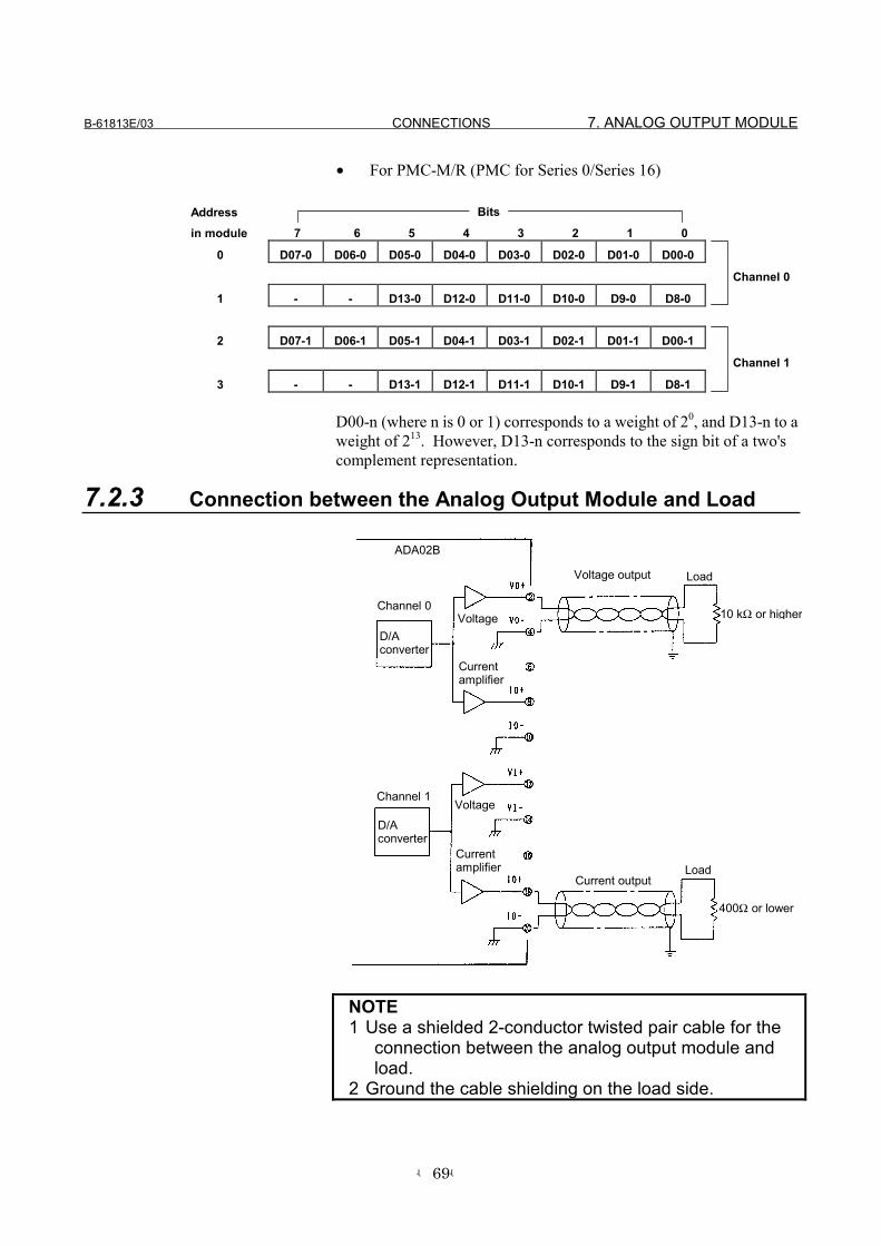
7.2.3 Connection between the Analog Output Module and Load
NOTE1 Use a shielded 2-conductor twisted pair cable for the
connection between the analog output module andload.
2 Ground the cable shielding on the load side.
Bits
ADA02B
Voltage output Load
Channel 0Voltage 10 kΩ or higher
D/Aconverter
D/Aconverter
Currentamplifier
Currentamplifier
Voltage
Load
Channel 1
Current output
400Ω or lower

8. HIGH SPEED COUNTER MODULE CONNECTIONS B-61813E/03
-70-
8 HIGH SPEED COUNTER MODULE
8.1 OUTLINE OF HIGH SPEED COUNTER MODULE
The high speed counter module consists of a counter which counts thepulses sent from a pulse generator such as a position detector in themachine tool and comparison registersfor comparing preset values withcounter data. The module can read the counter data andoutput theresults of comparison to the machine.The pulse counter module has two operation modes, A and B.Simplified configuration diagrams in modes A and B are shown below.
A. Mode A

B-61813E/03 CONNECTIONS 8. HIGH SPEED COUNTER MODULE
-71-
B. Mode B
to to

8. HIGH SPEED COUNTER MODULE CONNECTIONS B-61813E/03
-72-
8.2 SPECIFICATIONS OF HIGH SPEED COUNTER MODULE
8.2.1 Pulse counter
(1) Binary up/down counter (1)
(2) Counter capacity0 to 8, 388, 607
(3) Counter dataThe pulse counter can preset data and read count data.
8.2.2 Comparison function
(1) Mode A
A. Comparison register (23 bits)Comparison registers A, B, and C are provided. The valuesto be compared are preset in the comparison registers.
B. Comparison outputThe results (CMPA, CMPB, and CMPC) of comparing thecount data in the pulse counter with the data set in thecomparison registers are output.
C. Comparison output valuesThe comparison output values are set as listed in the tablebelow. The valuesdepend on the states of CMA, CMB, andCMC, the comparison mode signals from the PMC.
Counter value≦≦≦≦ comparison register value
Counter value> comparison register value
CMA=0CMB=0CMC=0
CMPA=0CMPB=0CMPC=0
CMPA=1CMPB=1CMPC=1
CMA=1CMB=1CMC=1
CMPA=1CMPB=1CMPC=1
CMPA=0CMPB=0CMPC=0
(2) Mode B
A. Comparison register (23 bits)There are 16 comparison registers #0,#1, ...,#15. The valuesto be compared are preset in the comparison registers. Thepreset value in a comparison register having a larger registernumber should be larger than that in a comparison registerhaving a smaller register number, as follows:Value in register #0 < value in register #1< ... < value inregister #14 < valuein register 15

B-61813E/03 CONNECTIONS 8. HIGH SPEED COUNTER MODULE
-73-
B. Comparison outputThe results (OUT0 to OUT7) of comparing the count data inthe pulse counter with the data set in the comparisonregisters are output.
C. Comparison output valuesThe count data in the pulse counter is compared with thevalues in the comparison registers in sequential order fromregister 0 until the count data is equal to or less than the valuein a comparison register. This enables a partition to bemadewhich includes the count data. Then the output data forthe partition (which is previously preset) is output. Eightoutput points (OUT0 to OUT7) are provided.If the count data is equal to the value in a comparison register,the data in the partition having the same number as theregister number is output.
Output data from partition #0 = 0HOutput data from partition #1 = 1HOutput data from partition #2 = 2HOutput data from partition #3 = 3HOutput data from partition #4 = 4HOutput data from partition #5 = 5HOutput data from partition #6 = 6HOutput data from partition #7 = 7HOutput data from partition #8 = 8HOutput data from partition #9 = 9HOutput data from partition #10 = 10HOutput data from partition #11 = 11HOutput data from partition #12 = 12HOutput data from partition #13 = 13HOutput data from partition #14 = 20HOutput data from partition #15 = 21HOutput data from partition #16 = FFH

8. HIGH SPEED COUNTER MODULE CONNECTIONS B-61813E/03
-74-
The output data is set as listed in the table below, depending on thecounter values in to above.
OUT7 6 5 4 3 2 1 0
0 0 0 0 0 0 0 0 0 0 0 0 0 0 0 1 0 0 0 0 0 0 1 0 0 0 0 0 0 0 1 0 0 0 1 0 0 0 0 0 0 0 1 0 0 0 0 1 1 1 1 1 1 1 1 1
8.2.3 Pulse Interface
The following three types of pulses are entered in the high speedcounter module.
A. Phase A/B pulses: The phase difference between these detection pulses is 90°
B. +/- pulses: These detection pulses are separated in the positive and negative directions.
Select either type of the detection pulse.C. Marker signal: Used to preset data in the pulse counter.
(1) Phase A/B pulse interfaceThe phase A/B pulses are selected when the PSEL signal is open.
A. Interface ICUse differential drivers (SN75113 or equivalent) at theoutput ports of the pulse generator.
B. Maximum frequency
Tmin. =8µS (minimum period)TDmin. =1.2µS (minimum time between edges)

B-61813E/03 CONNECTIONS 8. HIGH SPEED COUNTER MODULE
-75-
C. Count and directionA counter multiplied by four compared to phase A and Bpulses is provided. It counts positive when phase Aadvances before phase B and it counts negative when phaseB advances before phase A.Positive countAdvance of phase A before phase B
Negative countAdvance of phase B before phase A
(2) Positive/negative pulse interfacePositive and negative pulses are selected when the PSEL signal isconnected to 0 VDC.
A. Interface ICUse differential drivers (SN75113 or equivalent) at theoutput ports of the pulse generator.
B. Maximum frequency
Tmin. = 2µS (minimum period)TDmin. = 0.5µS (minimum pulse width)
(3) Marker signal
A. Interface ICUse differential drivers (SN75113 or equivalent) at theoutput ports of the pulse generator.
B. Minimum pulse width

8. HIGH SPEED COUNTER MODULE CONNECTIONS B-61813E/03
-76-
8.2.4 External contact input
The pulse counter module uses insulating receivers (having a voltagerating of 24 VDC) at the input ports. The following two types of signalinputs are provided.
(1) Marker enable signal input (ME)The contact of the marker enable signal is closed to make themarker signal valid.This enables data to be preset in the counter.
(2) Count stop signal input (CSP)The contact of the count stop signal is closed to stop the countoperation.
8.2.5 External contact output
Solid state relays are used for the contacts.
(1) Mode AThe comparison mode signal outputs A, B, C (CMPA, CMPB, andCMPC) are provided in mode A. These outputs indicate theresults of comparing the comparison registers A, B, and C with thepulse counter. The comparison output values are determineddepending on whether the control mode signals (CMA, CMB, andCMC) from the PMC are set to 1 or 0.
(2) Mode BThe results of comparing comparison register #0, comparisonregister #1, ..., comparison register #15 with the pulse counter areprovided in mode B. The comparison output indicates the valuesin the output data registers for the partitions in which the countdata is located. Eight output points are provided. (See Section8.2.2 (2))
8.2.6 Marker processing
(1) Mode A
A. Synchronization with markerThe counter value is set to the data in the counter presetregister at the rising edge of the first marker signal with theMS signal output from the PMC set to 1 and the contact ofthe marker enable signal input (ME) from the machineclosed.
B. Marker holdThe MH signal is set to 1 at the rising edge of the first markersignal with the MS signal output from the PMC set to 1 andthe contact of the marker enable signalinput (ME) from themachine closed. The MH signal is reset when the marker
B-61813E/03 CONNECTIONS 8. HIGH SPEED COUNTER MODULE
-77-
hold reset (MHR), an output signal from the PMC, is set to 1or the MS signal output from the PMC is set to 0.
(2) Mode B
A. Synchronization with markerWhen the MS signal output from the PMC is 1 and thecontact of the marker enable (ME) signal input from themachine is closed, the counter is set to the data in the counterpreset register at the rising edge of the first marker signal.
B. Maker holdWhen the MS signal output from the PMC is 1 and thecontact of the marker enable (ME) signal input from themachine is closed, the MH signal is set to 1 at the rising edgeof the marker signal. The MH signal is reset when the MSsignal output from the PMC is set to 0.
8.2.7 LED indicators
The high speed counter module has the following indicators.
(1) OK indicatorSee below Table.
(2) ALM0 and ALM1 indicatorsSee below Table.
(3) Phase A and B pulses (positive and negative pulses) input signalindicators (A and B)The phase A pulse input signal indicator is on when the phase Apulse input is active.The phase B pulse input signal indicator is on when the phase Bpulse input is active.
(4) Marker signal indicator (M)The marker signal indicator is on while the marker signal (MP)from the pulse generator is active.
(5) Count stop signal indicator (S)The count stop signal indicator is on when the contact of the countstop signal input sent from the machine is closed.
(6) Marker enable signal indicator (E)The marker enable signal indicator is on when the contact of themarker enable signal input sent from the machine is closed.
(7) Comparison result output indicators (OUT0, OUT1, OUT2,OUT3, OUT4, OUT5, OUT6, and OUT7)

8. HIGH SPEED COUNTER MODULE CONNECTIONS B-61813E/03
-78-
A. Mode AThe indicators OUT0, OUT1, and OUT2 correspond to thesignals CMPA, CMPB, and CMPC. OUT1 goes on whenCMPA goes on, OUT2 goes on when CMPB goes on, andOUT3 goes on when CMPC goes on.
B. Mode BThe indicators OUT0 - OUT7 go on corresponding to whenthe output data OUT0 - OUT7resulting from thecomparisons between the count data and comparisonresisters areset TO 1.
LED indicator panel
OK ALM0 ALM1 Explanation of alarmDisconnection alarm : OnSelf-diagnosis alarm, RAM error : OffSelf-diagnosis alarm, ROM errorWatch dog alarmNormal operation

B-61813E/03 CONNECTIONS 8. HIGH SPEED COUNTER MODULE
-79-
8.3 PMC INTERFACE
8.3.1 Mode A
(1) PMC I/O areaIn mode A, four input bytes and four output bytes are used as theI/O area. The bytes in the I/O area have the following names. Theinput and output directions arespecified on the basis of the PMC.The operation mode is set to mode A at power-on.
1) Output data (sent from PMC to high speed counter module)
0 CTRL (control)
+1 DTOH (higher 8-bit data)
+2 DTOM (middle 8-bit data)
+3 DTOL (lower 8-bit data)
2) Input data (entered from high speed counter module to PMC)
0 CNTS (counter H and status)
+1 CNTM (middle 8 bits of counter)
+2 CNTL (lower 8 bits of counter)
+3 STTS (status)
(2) PMC outputs (outputs from PMC)The PMC outputs are separated into control output CTRL anddata outputs DTOH, DTOM, and DTOL. As with normal DOs,the control outputs of bit 3 to bit 7 are controlled independently.The cotrol outputs of bit0 to bit2 constitute the SELECTindicating the target data specified by DTOH, DTOM, and DTOL.
1) Control output
CTRL7 6 5 4 3 2 1 0
MHR MS CE PRS SELECT
PRS : PresetCE : Count enableMS : Marker synchronizationMHR : Marker hold reset

8. HIGH SPEED COUNTER MODULE CONNECTIONS B-61813E/03
-80-
2) Details of DTOH, DTOM, and DTOLThe SELECT bits indicate the target data.
SELECT0 CCTR (comparison control)1 Counter preset data2 Comparison register A3 Comparison register B4 Comparison register C7 Change to mode B
NOTE1 Change to mode B: See Section 8.3.2, "Mode B".2 Detail of CCTR
DTOH7 6 5 4 3 2 1 0
CMC CMB CMA
The DTOM and DTOL are ignored.
(3) PMC inputs (inputs to PMC)The inputs to the PMC include the status and counter data. Thedata is shown below.
0 CNTS (counter H and status)
+1 CNTM (middle 8 bits of counter)
+2 CNTL (lower 8 bits of counter)
+3 STTS (status)
NOTE1 Details of CNTS
7 6 5 4 3 2 1 0
TRA
TRA : Transfer A
NOTE2 Details of STTS
7 6 5 4 3 2 1 0
TRB ALM CSP ME MH CMPC CMPB CMPA
CMPA : Comparison output ACMPB : Comparison output BCMPC : Comparison output CMH : Marker holdME : Marker enable
Counter H (most significant 7 bits)

B-61813E/03 CONNECTIONS 8. HIGH SPEED COUNTER MODULE
-81-
CSP : Count stopALM : Alarm (disconnection or watch dog alarm)TRB : Transfer B
8.3.2 Mode B
Change to mode BThe operation mode is set to mode A at power-on. The following datais output to the counter module and the mode changes from A to B. Themode cannot change from B to A.
0 CTRL : 0FH (SELECT = 7, PRS = 1)
+1 DTOH : 01H
+2 DTOM : 00H
+3 DTOL : 00H
(1) PMC I/O areaIn mode B, eight input bytes and four output bytes are used as theI/O area. The bytes in the I/O area have the following names. Theinput and output directions arespecified on the basis of the PMC.
1) Output data (sent from PMC to high speed counter module)
0 CTRL (control)
+1 DTOH (higher 8-bit data)
+2 DTOM (middle 8-bit data)
+3 DTOL (lower 8-bit data)
2) Input data (entered from high speed counter module to PMC)
0 CNTS (counter H and status)
+1 CNTM (middle 8 bits of counter)
+2 CNTL (lower 8 bits of counter)
+3 STTS (status)
+4 OUTD
+5 MODD
+6 Unused
+7 Unused
(2) PMC outputs (outputs from PMC)The PMC outputs are separated into control output CTRL anddata outputs DTOH, DTOM, and DTOL. As with normal DOs,the control outputs of bit 5 to bit 7 are controlled independently.The control outputs of bit 0 to bit 4 constitute SELECT indicatingthe target data specified by DTOH, DTOM, and DTOL.

8. HIGH SPEED COUNTER MODULE CONNECTIONS B-61813E/03
-82-
1) Control outputs
CTRL7 6 5 4 3 2 1 0
MS CE PRS SELECT
PRS : PresetCE : Count enableMS : Marker synchronization
2) Details of DTOH, DTOM, and DTOLThe SELECT bits indicate the target data.
SELECT Target data0 ~ 15 Comparison data 0 to comparison data 15
16 Output data for partition #0 to partition #2 DTOH:#0, M:#1,L:#2
17 Output data for partition #3 to partition #5 DTOH:#3, M:#4,L:#5
18 Output data for partition #6 to partition #8 DTOH:#6, M:#7,L:#8
19 Output data for partition #9 to partition #11 DTOH:#9, M:#10,L:#11
20 Output data for partition #12 to partition #14 DTOH:#12, M:#13,L:#14
21 Output data for partition #15 and partition #16 DTOH:#15,M:#16
22 Counter preset data(The numbers of DTOH, DTOM, and DTOL indicate the output datafor the partitions specified by the numbers.)
3) PMC inputs (inputs to PMC)The inputs to the PMC include the status and counter data.The data is shown below.
0 CNTS (counter H and status)
+1 CNTM (middle 8 bits of counter)
+2 CNTL (lower 8 bits of counter)
+3 STTS (status)
+4 OUTD
+5 MODD
+6 Not used
+7 Not used
NOTE1 Detail of CNTS
7 6 5 4 3 2 1 0
TRA Counter H (most significant 7 bits)

B-61813E/03 CONNECTIONS 8. HIGH SPEED COUNTER MODULE
-83-
TRA : Transfer A
NOTE2 Details of STTS
7 6 5 4 3 2 1 0
TRB ALM CSP ME MH OUT2 OUT1 OUT0
OUT0 : Bit 0 of comparison outputOUT1 : Bit 1 of comparison outputOUT2 : Bit 2 of comparison outputMH : Marker holdME : Marker enableCSP : Count stopALM : Alarm (disconnection or watch dog alarm)TRB : Transfer B
NOTE3 Detail of OUTD
7 6 5 4 3 2 1 0
OUT7 OUT6 OUT5 OUT4 OUT3 OUT2 OUT1 OUT0
OUT0 : Bit 0 of comparison outputOUT1 : Bit 1 of comparison outputOUT2 : Bit 2 of comparison outputOUT3 : Bit 3 of comparison outputOUT4 : Bit 4 of comparison outputOUT5 : Bit 5 of comparison outputOUT6 : Bit 6 of comparison outputOUT7 : Bit 7 of comparison output
NOTE4 Detail of MODD
7 6 5 4 3 2 1 0
MOD0
MOD0 : Set to 1 after the mode changes to B.
8.3.3 Details of PMC interface signals
(1) PMC inputs (inputs from PMC)
1) TRA and TRBThe counter data is valid when TRA is equal to TRB andinvalid when TRA is not equal to TRB.

8. HIGH SPEED COUNTER MODULE CONNECTIONS B-61813E/03
-84-
2) CMPA, CMPB, and CMPC (comparison output signals A, B,and C, only in mode A)The CMPA, CMPB, and CMPC signals are output signalsresulting from the comparison between the comparisonregisters A, B, and C and the counter data, respectively. Theoutput levels of CMPA, CMPB, and CMPC are determinedby the comparison mode signals CMA, CMB, and CMC.When CMA, CMB, and CMC are 0, and the counter data islarger than the values in comparison registers A, B, and C,CMPA, CMPB, and CMPC are set to 1.When CMA, CMB, and CMC are 1, and the counter data isequal to or less than the values in comparison registers A, B,and C, CMPA, CMPB, and CMPC are set to 1.
3) OUT0 to OUT 7 (comparison output signal 0 to comparisonoutput signal 7, only in mode B)OUT0 - OUT7 correspond to bit 0 to bit 7 in the comparisonresult output of a single byte.
4) MH (marker hold signal)The marker hold signal MH is set to 1 at the rising edge ofthe marker signal whenthe marker enable signal is 1. Themarker hold signal is reset when MHR=1 or MS=0. (In modeB, the marker hold signal MH is reset only when MS=0.)
5) ME (marker enable signal)The marker enable signal ME enables the marker signal asfollows:
ME=1: Marker signal enabledME=0: Marker signal disabled
6) CSP (count stop signal)The counter stops counting when the contact for the externalinput signal CSP is closed.
7) ALM (alarm signal)The alarm signal ALM is set to 1 if the signal line for thecount pulse or the marker signal is disconnected or short-circuited.ALM is also set to 1 when the watch dog alarm is activated.
(2) PMC outputs (outputs from PMC)
1) SELECT (selection signal)The SELECT signal selects the register in which data will beset. That is, the signal specifies the register for presettingdata. The SELECT signal should be set when or before thePRS signal is reversed.

B-61813E/03 CONNECTIONS 8. HIGH SPEED COUNTER MODULE
-85-
2) PRS (preset signal)The PRS signal presets data in registers. If data is set inDTOH, DTOM, and DTOL and then PRS is reversed, thedata is set in the register specified by SELECT. Reversingthe PRS signal means that PRS changes from level 0 to level1 or vise versa.DTOH, DTOM, DTOL, and SELECT should not be changedwithin two scans after the PRS is reversed. Also, the PRSmust not reversed again within this period.When SELECT=1, data is set in both the counter presetregister and the counter.Data is set by setting the first PRS to 1 after power-on or afterthe mode changesto B.
3) CE (count enable signal)The CE signal determines whether the counter counts. Whenthe CE is set to 1 and the external input signal CSP closes thecontact, the counter retains its value, instead of counting.When CE = 1 and the CSP external input contact is open, thecounter counts input pulses. Presetting the counter requiresmaintaining CE = 0.
4) MS (marker synchronization signal)The MS signal determines whether marker synchronizationis provided. When the MS is 1 and the the contact of externalinput signal ME is closed, the counter is preset to the value inthe counter preset register at the rising edge of thefirstmarker signal. If the MS is set to 0 then set to 1 or theMHR is set to 1 then setto 0, marker synchronization isprovided again.(The MHR signal is not included in mode B.)
5) MHR (marker hold reset signal, only in mode A)The MHR signal resets the marker hold (MH) signal which isoutput to the PMC. TheMHR is set to 1 to reset the markerhold signal.
6) CMA, CMB, and CMC (comparison mode signals A, B, andC, only in mode A)The CMA, CMB, and CMC signals specify the levels of thecomparison outputs A, B, and C (CMPA, CMPB, andCMPC), respectively.When CMA, CMB, and CMC are 0, and the value of thecounter is larger than the values in comparison registers A, B,and C, CMPA, CMPB, and CMPC are set to 0.When CMA, CMB, and CMC are 1, and the value of thecounter is equal to or less than the values in comparisonregisters A, B, and C, CMPA, CMPB, and CMPC are set to1.

8. HIGH SPEED COUNTER MODULE CONNECTIONS B-61813E/03
-86-
8.4 TOTAL CONNECTION OF HIGH SPEED COUNTERMODULE
8.4.1 Connection diagram
HEROSE(HIF-3BA-20D-2.54R)(A63L-0001-0472#S20)

B-61813E/03 CONNECTIONS 8. HIGH SPEED COUNTER MODULE
-87-
8.4.2 Connector signal list
JA910 20 +5V
9 +5V 198 PSEL 18 +5V
7 LGND 176 *MKS 16 LGND
5 MKS 184 *PBS 14 LGND
3 PBS 132 *PAS 12 LGND
1 PAS 11
PAS : Phase A pulse input signal (Negative pulse inputsignal)(positive)
*PAS : Phase A pulse input signal (Negative pulse inputsignal)(negative)
PBS : Phase B pulse input signal (Positive pulse inputsignal)(positive)
*PBS : Phase B pulse input signal (Positive pulse inputsignal)(negative)
MKS : Marker signal (positive)*MKS : Marker signal (negative) PSEL : Pulse select signal +5V : 5V (output from this module)LGND : 0V
C49A B
01 ME02 CSP03 COM1040506 OUT0 OUT407 OUT1 OUT508 OUT2 OUT609 OUT3 OUT710 COM2 COM3
ME : Marker enable signal inputCSP : Counter stop signal inputOUT0 : Comparison result outputOUT1 : Comparison result outputOUT2 : Comparison result outputOUT3 : Comparison result outputOUT4 : Comparison result outputOUT5 : Comparison result outputOUT6 : Comparison result outputOUT7 : Comparison result outputCOM1 : Common signal for ME and CSPCOM2 : Common signal for comparison result
output 0 to comparison result output 3COM3 : Common signal for comparison result
output 4 to comparison result output 7

8. HIGH SPEED COUNTER MODULE CONNECTIONS B-61813E/03
-88-
8.5 CONNECTION WITH PULSE GENERATOR
8.5.1 Use of phase A and B pulses
Recommended cableA66L-0001-0286 (#20AWG×7, #24AWG×3 Pairs)

B-61813E/03 CONNECTIONS 8. HIGH SPEED COUNTER MODULE
-89-
8.5.2 Use of positive/negative pulses
Recommended cableA66L-0001-0286 (#20AWG×8, #24AWG×3 Pairs)

8. HIGH SPEED COUNTER MODULE CONNECTIONS B-61813E/03
-90-
8.6 CONNECTION WITH POWER MAGNETICS CABINET

B-61813E/03 CONNECTIONS 8. HIGH SPEED COUNTER MODULE
-91-
8.7 I/O SIGNALS CONVENTIONS
8.7.1 Solid state relay output signals (OUT0 to OUT7)
The solid state relay output signals drive relays in the power magneticscabinet and indicator LEDs.
(1) Solid state relays
i) Maximum load current at output-on250 mA: Up to three outputs set to on125 mA: Eight outputs set to on
ii) Saturation voltage at output-onNot more than 6xIL V (IL: load current)
iii) Withstand voltage at output-off30 VDC max. even for instantaneous voltage
iv) Leak current at output-offNot more than 100µA
(2) Output circuit
(3) Always install spark arresters when inductive loads such as relaysare connected in the machine. Insert the spark arresters as near theload as possible (less than 20 cm). When capacitive loads areused in the machine, insert current limiting resistors in series withthe loads to prevent the instantaneous current and voltage fromexceeding the rated values.
(4) If a lamp is turned on by a solid state relay output, the resultingsurge current may damage the solid state relay. Thus, as shown inthe figure below, provide a protective resistor to prevent theinstantaneous current and voltage from exceeding the ratedvalues.

8. HIGH SPEED COUNTER MODULE CONNECTIONS B-61813E/03
-92-
8.7.2 DC input signals (ME and CSP)
The DC input signals (such as relay contact signal) are sent from themachine (control circuit) to the pulse counter module.
(1) Input conditionsOn voltage and current: 15 VDC or more, 4.5 mA or moreOff voltage and current: 6 VDC or less, 2 mA or lessResponse time: 20 mA or less
(2) Voltage and polarityVoltage : 24 VDC +10%, -20%Polarity : Positive or negative polarity available (The power is
not supplied from the pulse counter module.)
(3) Logical correspondence
Contact LogicOpen 0
Closed 1
(4) Receiver circuit of DC input signal
Machine Pulse counter module
24 VDC +10% -20%

B-61813E/03 CONNECTIONS 8. HIGH SPEED COUNTER MODULE
-93-
8.8 SUPPLEMENT
8.8.1 Configuration of mode A
How mode A is configured is shown below. The contents of the CNTS,CNTM, CNTL, and STTS on a high-speed counter module are sent tothe X area assigned on the master via the I/O link. The contents of theY area assigned on the master are sent to CTRL, DTOH, DTOM, andDTOL on the high-speed counter module, via the I/O link.
*** F.21-1 ***1. Master2. Via the I/O link(period of 2 ms)3. High-speed counter
Master
Via the I/O link(period of 2 ms)
High-speed counter

8. HIGH SPEED COUNTER MODULE CONNECTIONS B-61813E/03
-94-
8.8.2 Counter presetting and counting
(1) The following table lists the information related to counterpresetting. The MH signal can be reset either by setting the MHR(bit 7) of the CTRL (control) to 1 or by resetting the MS (bit 6) ofthe CTRL to 0. See control examples 1 and 2.
Condition StatusMHR of CTRL MS of CTRL ME of external
signalMKS of external
signalME of STTS MH of STTS
Counterpresetting
0 1 Contact "Closed Initial ↑ 1 1
MH signalresetting (1)
× 0 × × × 0
MH signalresetting (2)
1 × × × × 0
• Contact "Closed" means that 24 V is applied to the MEterminal.
• × means that the bit can be either 0 or 1. (× for the ME bit ofthe STTS means that the bit corresponds to the status of theME bit of the external signal.)
Control example 1:(Hatching means that the bit can be either 0 or 1.)
Control example 2:(Hatching means that the bit can be either 0 or 1.)
Counter
Counter
Preset Preset
PresetPreset

B-61813E/03 CONNECTIONS 8. HIGH SPEED COUNTER MODULE
-95-
(2) Information related to countingCounting starts and stops under the conditions listed below.
CE of CTRL CSP of externalsignal
PSEL of externalsignal
CSP of STTS
Count (A/B phase pulse) 1 Contact "Open" Open 0Count (+/- pulse) 1 Contact "Open" Connected to 0 V 0Counting stop (1) 0 × × ×Counting stop (2) × Contact "Closed" × 1
• Contact "Closed" means that 24 V is applied to the CSPterminal. (1 or POS)
• Contact "Open" means that the CSP terminal is open. (0 orNEG)
• × means that the bit can be either 0 or 1. (× for the CSP bit ofthe STTS means that the bit corresponds to the status of theCSP bit of the external signal.)
8.8.3 Setting data
Data for some models (such as the FS15 and FS18) is in the oppositeorder to that of the NC data. In this case, convert (rearrange) the data inbyte units.
[Example of setting]CTRL 7 6 5 4 3 2 1 0
DTOH PRS SELECT
DTOM
DTOL
Example 1 : To preset the counter preset register with a specific value(the counter is also set to this value), follow the stepsbelow.
(1) Preset the DTOH, DTOM, and DTOL with a desired value.(2) Set SELECT to 001.(3) Reverse the setting of the PRS (from 0 to 1 or from 1 to 0).(4) Wait for two scanning periods.
• Another method for presetting the counter is to use the MKSexternal signal (see Section 3.1). It takes a maximum of 5 msto preset using the first method, while it takes only amaximum of 100 µs to preset using the MKS external signal.
Example 2 : To set the comparison control register with the setting (0or 1) of CMA, CMB, and CMC, follow the steps below.
(1) Set DTOH bits 0, 1, and 2 to the desired data.(2) Set SELECT to 000.(3) Reverse the setting of the PRS (from 0 to 1 or from 1 to 0).(4) Wait for two scanning periods.

8. HIGH SPEED COUNTER MODULE CONNECTIONS B-61813E/03
-96-
Example 3 : To set comparison register B to a desired comparisonvalue, follow the steps below.
(1) Set DTOH, DTOM, and DTOL to the desired comparison value.(2) Set SELECT to 011.(3) Reverse the setting of the PRS (from 0 to 1 or from 1 to 0).(4) Wait for two scanning periods.
The result of comparing comparison registers A, B, and C with thepulse counter is output via OUT0 to OUT2 of connector C49 of thiscounter module (A → OUT0, B → OUT1, and C → OUT2).Their output status is output via OUT0 to OUT2 of the LED indicationpanel (A → OUT0, B → OUT1, and C → OUT2).The result of comparison can be confirmed by checking STTS bits 0, 1,and 2 (CMPA, CMPB, and CMPC) with the PMC.

B-61813E/03 CONNECTIONS 8. HIGH SPEED COUNTER MODULE
-97-
8.8.4 Reading data
The CNTS and STTS are two of the four input bytes. The mostsignificant bit, TRA, of the CNTS and the most significant bit, TRB, ofthe STTS can be used to determine whether the count data is correct. Ifboth TRA and TRB are 0 or 1, the count data is correct.In almost all cases, both TRA and TRB will be 0 or 1 when you viewthe diagnostic display. (Do not determine that the data has not changedbecause of the fact that the TRA and TRB do not become 0 or 1alternately.) Note that the count data does not take a negativevalue.
(CNTS)
TRA Counter H
(STTS)
TRB ALM CSP ME MH CMPC CMPB CMPA
TRA TRB Validity
0 0 Correct
0 1 Incorrect
1 0 Incorrect
1 1 Correct
The counter assumes the following data when it is incremented ordecremented.
0000000 00000000 00000010 0000000 00000000 00000001 0000000 00000000 00000000 1111111 11111111 11111111
to 0000000 00000000 00000011 0000000 00000000 00000010 0000000 00000000 00000001 0000000 00000000 00000000 1111111 11111111 11111111 1111111 11111111 11111110 1111111 11111111 11111101 1111111 11111111 11111100
The square represents the TRA. (The most significant bit is the TRA.It is not a sign bit.)
Increment
Decrement
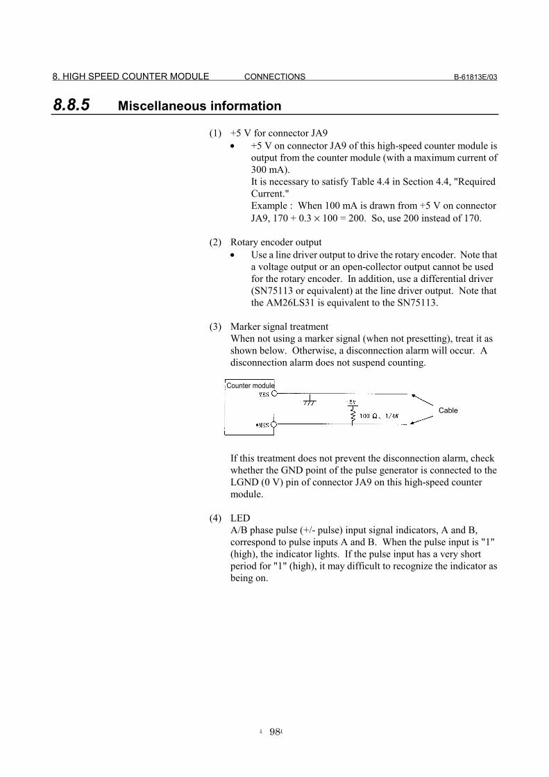
8. HIGH SPEED COUNTER MODULE CONNECTIONS B-61813E/03
-98-
8.8.5 Miscellaneous information
(1) +5 V for connector JA9• +5 V on connector JA9 of this high-speed counter module is
output from the counter module (with a maximum current of300 mA).It is necessary to satisfy Table 4.4 in Section 4.4, "RequiredCurrent."Example : When 100 mA is drawn from +5 V on connectorJA9, 170 + 0.3 × 100 = 200. So, use 200 instead of 170.
(2) Rotary encoder output• Use a line driver output to drive the rotary encoder. Note that
a voltage output or an open-collector output cannot be usedfor the rotary encoder. In addition, use a differential driver(SN75113 or equivalent) at the line driver output. Note thatthe AM26LS31 is equivalent to the SN75113.
(3) Marker signal treatmentWhen not using a marker signal (when not presetting), treat it asshown below. Otherwise, a disconnection alarm will occur. Adisconnection alarm does not suspend counting.
If this treatment does not prevent the disconnection alarm, checkwhether the GND point of the pulse generator is connected to theLGND (0 V) pin of connector JA9 on this high-speed countermodule.
(4) LEDA/B phase pulse (+/- pulse) input signal indicators, A and B,correspond to pulse inputs A and B. When the pulse input is "1"(high), the indicator lights. If the pulse input has a very shortperiod for "1" (high), it may difficult to recognize the indicator asbeing on.
Cable
Counter module

B-61813E/03 CONNECTIONS 9. TEMPERATURE INPUT MODULE
-99-
9 TEMPERATURE INPUT MODULE
9.1 OVERVIEW
A temperature input module is used to measure the temperature ofmachine tools and similar equipment. The temperature input modulecan be either of the following, depending on the type of the sensor used.
• Thermoresistance-type temperature input module: ATI04A• Thermocouple-type temperature input module: ATI04B
These modules can measure temperature on up to four channels. Forthe thermoresistance-type temperature input module, either JPt100Ω orPt100Ω can be selected. For the thermocouple-type temperature inputmodule, either K or J thermocouple input can be selected. Thisselection is made using the PMC user program (ladder).
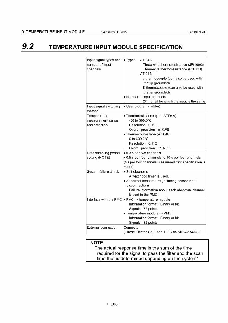
9. TEMPERATURE INPUT MODULE CONNECTIONS B-61813E/03
-100-
9.2 TEMPERATURE INPUT MODULE SPECIFICATION
Input signal types andnumber of inputchannels
• Types ATI04AThree-wire thermoresistance (JPt100Ω)Three-wire thermoresistance (Pt100Ω)
ATI04BJ thermocouple (can also be used withthe tip grounded)K thermocouple (can also be used withthe tip grounded)
• Number of input channels2/4, for all for which the input is the same
Input signal switchingmethod
• User program (ladder)
Temperaturemeasurement rangeand precision
• Thermoresistance type (ATI04A)-50 to 300.0°CResolution 0.1°COverall precision ±1%FS
• Thermocouple type (ATI04B)0 to 600.0°CResolution 0.1°COverall precision ±1%FS
Data sampling periodsetting (NOTE)
• 0.3 s per two channels• 0.5 s per four channels to 10 s per four channels(4 s per four channels is assumed if no specification ismade)
System failure check • Self-diagnosisA watchdog timer is used.
• Abnormal temperature (including sensor input disconnection)
Failure information about each abnormal channelis sent to the PMC.
Interface with the PMC • PMC → temperature moduleInformation format: Binary or bitSignals: 32 points
• Temperature module → PMCInformation format: Binary or bitSignals: 32 points
External connection Connector(Hirose Electric Co., Ltd.: HIF3BA-34PA-2.54DS)
NOTEThe actual response time is the sum of the timerequired for the signal to pass the filter and the scantime that is determined depending on the system1

B-61813E/03 CONNECTIONS 9. TEMPERATURE INPUT MODULE
-101-
9.3 PMC INTERFACE
9.3.1 PMC I/O area
This temperature module uses an input/output area consisting of fourbytes for input and the same number of bytes for output. Each byte ofthe input/output area has the following meanings. The terms "input"and "output" are used in reference to the PMC. When input/outputaddresses are assigned to the module, "/4" is used as the module name.
1) Output (PMC → temperature module)
Addresses in the module0 DO07 to DO00 Period for 4-channel automatic measurement
mode (lower 8 bits)+1 DO15 to DO08 Period for 4-channel automatic measurement
mode (higher 8 bits)+2 DO23 to DO16 Module setting data and timing data+3 DO31 to DO24 Module setting data and timing data
2) Input (temperature module → PMC)
Addresses in the module0 DI07 to DI00 CH1 temperature data, CH3 temperature data, or
abnormality data (lower 8 bits)+1 DI12 to DI08 CH1 temperature data, CH3 temperature data, or
abnormality data (higher 5 bits)DI15 to DI13 Status signal
+2 DI23 to DI16 CH2 temperature data, CH4 temperature data, orabnormality data (lower 8 bits)
+3 DI28 to DI24 CH2 temperature data, CH4 temperature data, orabnormality data (higher 5 bits)
DI31 to DI29 Status signal
NOTEIf you are using the PMC-N, NA, or QA (the PMC forSeries 15 or F-D Mate), all addresses up to thoselisted above can be used without modifying them ifthe data is manipulated in byte (8-bit) units. Whenmanipulating data in word (16-bit) units, note that thebyte addresses are transposed as shown below.
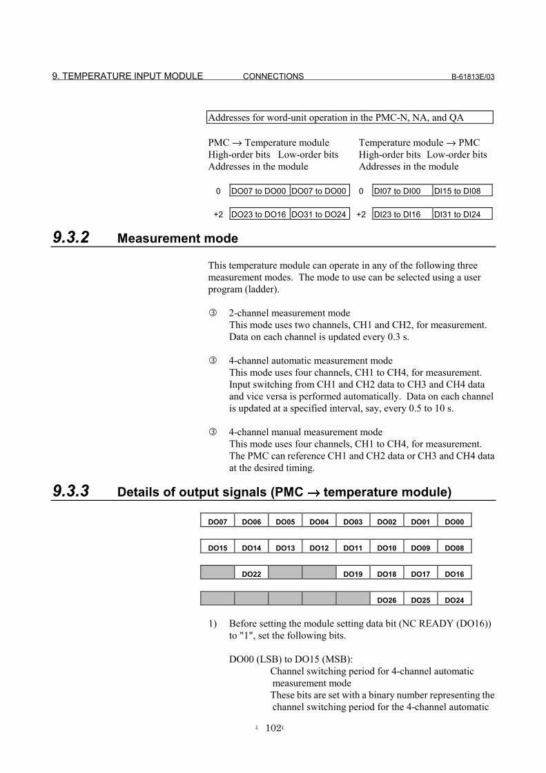
9. TEMPERATURE INPUT MODULE CONNECTIONS B-61813E/03
-102-
Addresses for word-unit operation in the PMC-N, NA, and QA
PMC → Temperature module Temperature module → PMCHigh-order bits Low-order bits High-order bits Low-order bitsAddresses in the module Addresses in the module
0 DO07 to DO00 DO07 to DO00 0 DI07 to DI00 DI15 to DI08
+2 DO23 to DO16 DO31 to DO24 +2 DI23 to DI16 DI31 to DI24
9.3.2 Measurement mode
This temperature module can operate in any of the following threemeasurement modes. The mode to use can be selected using a userprogram (ladder).
2-channel measurement modeThis mode uses two channels, CH1 and CH2, for measurement.Data on each channel is updated every 0.3 s.
4-channel automatic measurement modeThis mode uses four channels, CH1 to CH4, for measurement.Input switching from CH1 and CH2 data to CH3 and CH4 dataand vice versa is performed automatically. Data on each channelis updated at a specified interval, say, every 0.5 to 10 s.
4-channel manual measurement modeThis mode uses four channels, CH1 to CH4, for measurement.The PMC can reference CH1 and CH2 data or CH3 and CH4 dataat the desired timing.
9.3.3 Details of output signals (PMC →→→→ temperature module)
DO07 DO06 DO05 DO04 DO03 DO02 DO01 DO00
DO15 DO14 DO13 DO12 DO11 DO10 DO09 DO08
DO22 DO19 DO18 DO17 DO16
DO26 DO25 DO24
1) Before setting the module setting data bit (NC READY (DO16))to "1", set the following bits.
DO00 (LSB) to DO15 (MSB):Channel switching period for 4-channel automaticmeasurement modeThese bits are set with a binary number representing thechannel switching period for the 4-channel automatic

B-61813E/03 CONNECTIONS 9. TEMPERATURE INPUT MODULE
-103-
measurement mode. They need not be set for the 2-channel mode.The period can be varied in a range between 0.5 s and10 s. When setting the bits, use a value ten times thedesired period.(Example) 2 s → 20 (14h)The valid data range is between 5 and 100 (64h). Anyvalue out of this range is regarded as being 40 (28h),that is, 4 s. If nothing is specified, a period of 4 s isagain assumed.
DO17 : Module typeThis bit is set according to the type of the temperaturemodule being used.
0 :Thermocouple-type module (ATI04B)1 :Thermoresistance-type module (ATI04A)
DO18 : Sensor typeThis bit is set according to the type of the temperaturesensor being used.
• ATI04A0 :Pt1 :JPt
• ATI04B0 :K1 :J
DO19 : Reserved for future useThis bit must always be set to "0".
DO24 : Number of channelsThis bit is used to specify the number of channels to bemeasured.
0 :2 channels1 :4 channels (if 1 is selected, DO25 must also be
used.)
DO25 : 4-channel mode specificationThis bit is used to select the 4-channel mode to be used.
0 :Automatic measurement (the period is specifiedusing DO00 to DO15.)
1 :Manual measurement (a request is issued usingDO22 and DO26 at every data read.)

9. TEMPERATURE INPUT MODULE CONNECTIONS B-61813E/03
-104-
2) Timing dataDO16 : NC READY
When the power is switched on, this bit is set to "1" tocause the module setting data to be set in thetemperature module.The NC READY bit is enabled only once after thepower is switched on. To rewrite the module settingdata, switch the power off and then on again.
DO22 : READ requestThis bit serves as the timing signal used in 4-channelmanual measurement mode. Setting the bit to "1"issues a request for temperature data. When the inputsignal data READY signal becomes "1", read thetemperature data.This bit need not be set for 2-channel mode.
NOTEAfter setting the NC READY bit to "1", wait for onesecond, and then set the READ request to "1".
DO26 : Channel selectThis bit is used to specify channel switching for 4-channel manual measurement mode.
0: Channels 1 and 21: Channels 3 and 4
NOTESee Section 9.5, "Timing Charts," for concreteexplanations about how to handle the timing data.
9.3.4 Details of input signals (temperature module →→→→ PMC)
1) Status signals and CH1 temperature data, CH3 temperature data,or abnormality data
DI07 DI06 DI05 DI04 DI03 DI02 DI01 DI00
DI15 DI14 DI13 DI12 DI11 DI10 DI09 DI08
READ request1 s or longer

B-61813E/03 CONNECTIONS 9. TEMPERATURE INPUT MODULE
-105-
• Status signalsDI13 : Abnormality sign bit
1 : This bit is set to "1" when the temperatureinput is abnormal. DI00 to DI12 are usedto describe the abnormality.
0 : DI00 to DI12 are used to indicate thetemperature data.
DI14 : CH1 data READY1 : Read the CH1 temperature data from DI00
to DI12 when this bit is set to "1".
DI15 : CH3 data READY1 : Read the CH3 temperature data from DI00
to DI12 when this bit is set to "1".
• CH1 temperature data, CH3 temperature data, orabnormality dataDI00 (LSB) to DI12 (MSB):
These bits indicate temperature input data(CH1/CH3) or abnormality data.
Temperature input dataThe temperature input data is in binary. It is ten times the actualtemperature.Example
(83EDh → 1005 → 100.5)The highest three bits are status signals.
For the thermoresistance-type module (ATI04A), the DI12 bit is a signbit. (Negative data is represented in two's complement.)Example
(9F9Ch → -10.0)The highest three bits are status signals.
Abnormality dataIf an abnormality occurs in the input data or in the module, the DI13 bit(status signal) becomes "1", resulting in the display changing fromtemperature input data to abnormality data. Abnormality data isassigned to these bits as listed below:
DI00 : CH1 input out of scale--the current temperature fallsoutside the measurable range.
DI01 : CH1 input burn-out--the cable or connector has beendetached.
DI02 : CH3 input out of scale--the current temperature fallsoutside the measurable range.
DI03 : CH3 input burn-out--the cable or connector has beendetached.
DI04 : Cold-junction abnormality (only for thermocouple-typeinput module)--the temperature of the terminal board unitfalls outside the measurable range.

9. TEMPERATURE INPUT MODULE CONNECTIONS B-61813E/03
-106-
DI05 : System error--the internal circuit is abnormal.DI06 : Wrong module--other than the correct module has been
installed.
2) Status signals, CH2 temperature data, CH4 temperature data, orabnormality data
DI23 DI22 DI21 DI20 DI19 DI18 DI17 DI16
DI31 DI30 DI29 DI28 DI27 DI26 DI25 DI24
• Status signalsDI129 : Abnormality sign bit
1 : This bit becomes "1" when the temperatureinput becomes abnormal. DI16 to DI28 areused to describe the abnormality.
0 : DI16 to DI28 are used to indicate thetemperature data.
DI30 : CH2 data READY1 : Read the CH2 temperature data from DI16
to DI28 when this bit is set to "1".
DI31 : CH4 data READY1 : Read the CH4 temperature data from DI16
to DI28 when this bit is set to "1".• CH2 temperature data, CH4 temperature data, or
abnormality dataDI16 (LSB) to DI28 (MSB):
These bits indicate temperature input data(CH2/CH4) or abnormality data.
Temperature input dataThe temperature input data is in binary. It is ten times the actualtemperature.Example
(41F3h → 0499 → 49.9)The highest three bits are status signals.
For a thermoresistance-type module (ATI04A), the DI28 bit is a signbit. (Negative data is represented in two's complement.)Example
(5FFBh → -0.5)The highest three bits are status signals.

B-61813E/03 CONNECTIONS 9. TEMPERATURE INPUT MODULE
-107-
Abnormality dataIf an abnormality occurs in the input data or the module, the DI29 bit(status signal) is set to "1", resulting in the display changing fromtemperature input data to abnormality data. Abnormality data isassigned to these bits as listed below:
DI16 : CH2 input out of scale--the current temperature fallsoutside the measurable range.
DI17 : CH2 input burn-out--the cable or connector has beendetached.
DI18 : CH4 input out of scale--the current temperature fallsoutside the measurable range.
DI19 : CH4 input burn-out--the cable or connector has beendetached.
DI20 : Cold-junction abnormality (only for thermocouple-typeinput module)--the temperature of the terminal board unitfalls outside the measurable range.
DI21 : System error--the internal circuit is abnormal.DI22 : Wrong module--other than the correct module has been
installed.
9.4 COMPLETE CONNECTION OF TEMPERATURE INPUTMODULE
9.4.1 Temperature input module connection diagram
(There are two types of terminal board units, the first for athermoresistance-type module and the second for a thermocouple-typemodule.)See Section 9.7 for explanations about the dimensions of the terminalboard.
Temperature sensors •Thermoresistance •J/K thermocouple
HiroseElectric Co., Ltd.
Terminal board unit
Temperature input module
Cable
Hirose Electric Co., Ltd.

9. TEMPERATURE INPUT MODULE CONNECTIONS B-61813E/03
-108-
9.4.2 Connector signal lists
1) Thermoresistance input moduleATI04A
Channel Pin No. Pin No.Channel 1 - 1A 1BChannel 1 + 2A 2BChannel 1 + 3A 3BChannel 2 - 4A 4BChannel 2 + 5A 5BChannel 2 + 6A 6BChannel 3 - 7A 7BChannel 3 + 8A 8BChannel 3 + 9A 9BChannel 4 - 10A 10BChannel 4 + 11A 11BChannel 4 + 12A 12B
Unusable 13A 13BUnusable 14A 14BUnusable 15A 15BUnusable 16A 16BUnusable 17A 17B
2) Thermocouple input moduleATI04B
Channel Pin No. Pin No.Channel 1 - 1A 1BChannel 1 + 2A 2B
Unusable 3A 3BChannel 2 - 4A 4BChannel 2 + 5A 5B
Unusable 6A 6BChannel 3 - 7A 7BChannel 3 + 8A 8B
Unusable 9A 9BChannel 4 - 10A 10BChannel 4 + 11A 11B
Unusable 12A 12BCold-junction compensation element A 13A 13B
Cold-junction compensation element B1 14A 14BCold-junction compensation element B2 15A 15B
Unusable 16A 16BUnusable 17A 17B
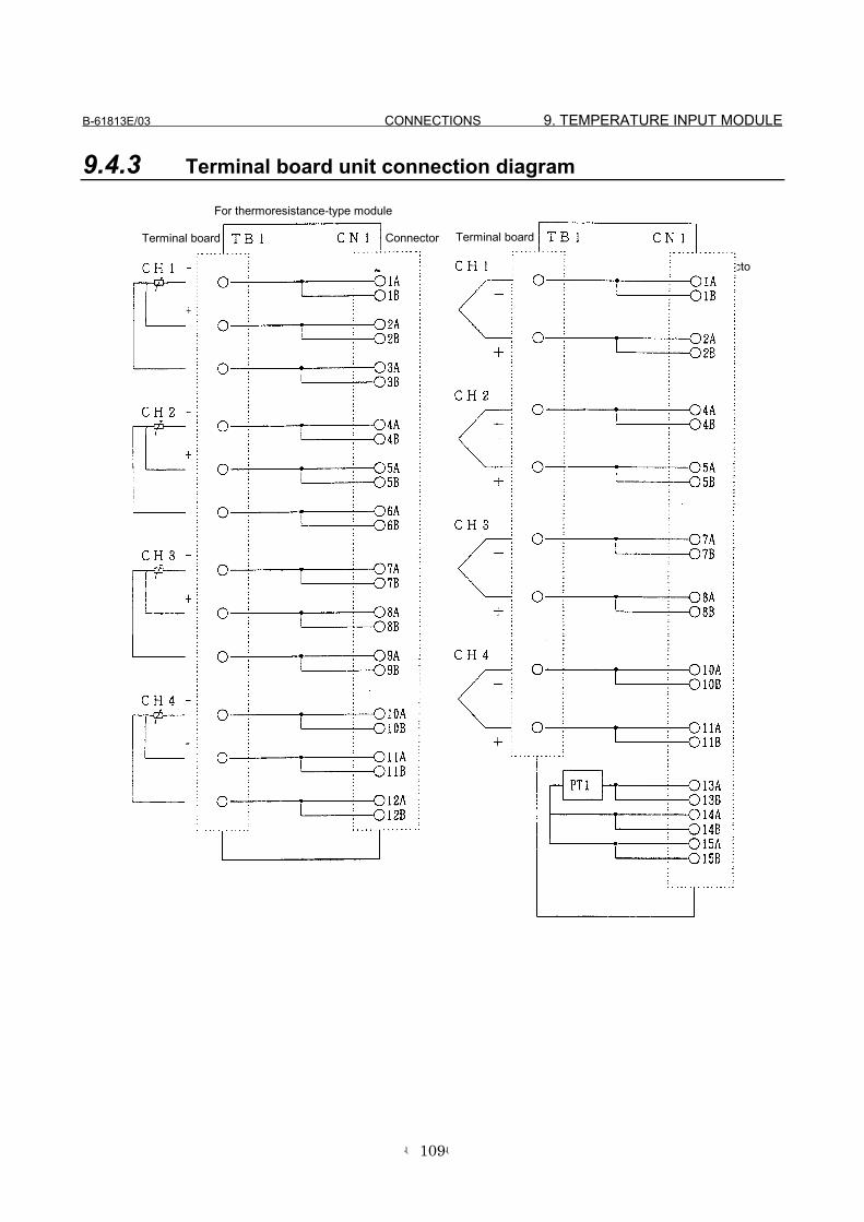
B-61813E/03 CONNECTIONS 9. TEMPERATURE INPUT MODULE
-109-
9.4.3 Terminal board unit connection diagram
For thermocouple-type module
Connecto
Temperature sensors•Thermoresistance•J/K thermocouple
For thermoresistance-type module
Terminal board Connector Terminal board

9. TEMPERATURE INPUT MODULE CONNECTIONS B-61813E/03
-110-
9.5 TIMING CHARTS
(1) 2-channel mode
NOTEThe actual response time is the sum of the timerequired to pass the filter and the scan time that isdetermined depending on the system.
(2) 4-channel automatic measurement mode
NOTEThe actual response time is the sum of the timerequired to pass the filter and the scan time that isdetermined depending on the system.
(3) 4-channel manual measurement mode
Temperature data
0.3s (NOTE)
CH1/CH2 data READY
5ms
NC READY
Temperature data
CH1/CH2 data READYCH3/CH4 data READY
Specified period (0.5 to 10 s) (NOTE)
Channel select
READ request1 s or longer
Temperaturedata
CH1/CH2 dataREADYCH3/CH4 dataREADY

B-61813E/03 CONNECTIONS 9. TEMPERATURE INPUT MODULE
-111-
9.6 MEASUREMENT EXAMPLES
(1) 2-channel mode(a) Flowchart
Specify the module type (DO17).0 : Thermocouple module1 : Thermoresistance module
Specify the sensor type (DO18).0 : Pt/K1 : JPt/J
Reset the number of channels bit(DO24) to "0".
Set NC READY (DO16) to "1".
When CH2 data READY (DI30 of input signal) becomes"1", input signals DI16 to DI28 represent CH2 data.
START
Now ready tomeasure.
When CH1 data READY (DI14 of input signal) becomes"1", input signals DI00 to DI12 represent CH1 data.
*Check that NC READY(DO16) and DO19 are "0".

9. TEMPERATURE INPUT MODULE CONNECTIONS B-61813E/03
-112-
(b) Ladder exampleThe following measurement and ladder examples applywhen a thermoresistance module with Pt is used formeasurement.PMC measurement
GROUP BASE SLOT NAME GROUP BASE SLOT NAMEX000 0 0 1 /4 Y000 0 0 1 /4X001 0 0 1 /4 Y001 0 0 1 /4X002 0 0 1 /4 Y002 0 0 1 /4X003 0 0 1 /4 Y003 0 0 1 /4
NOTESet the ladder scan time to 0.25 s or less.This example of ladder use is for the second level.R0.0 is used as a normally open relay.
Ladder
Specify the module.
(thermoresistance-type module)Specify the sensor (Pt).
Specify the number of channels (twochannels).
NC READY (When R1.0 becomes"1", NC READY becomes "1" to startmeasurement.)
When CH1 data READY is "1", CH1temperature data is sent to R010 toR011.
When CH2 data READY is "1", CH2temperature data is sent to R012 toR013.

B-61813E/03 CONNECTIONS 9. TEMPERATURE INPUT MODULE
-113-
(2) 4-channel automatic measurement mode(a) Flowchart
Specify the module type (DO17).0 : Thermocouple module1 : Thermoresistance module
Specify the sensor type (DO18).0 : Pt/K1 : JPt/J
Set the number of channels bit (DO24) to"1".
Set NC READY (DO16) to "1".
When CH2 data READY (DI30 of input signal) becomes"1", input signals DI16 to DI28 represent CH2 data.
START
Now ready tomeasure.
When CH1 data READY (DI14 of input signal) becomes"1", input signals DI00 to DI12 represent CH1 data.
Set the 4-channel mode specification bit (DO25)to "0".
Specify the channel switching period (DO00 toDO15).
When CH3 data READY (DI15 of input signal) becomes"1", input signals DI00 to DI12 represent CH3 data.
When CH4 data READY (DI31 of input signal) becomes"1", input signals DI16 to DI28 represent CH4 data.
*Check that NC READY(DO16) and DO19 are "0".

9. TEMPERATURE INPUT MODULE CONNECTIONS B-61813E/03
-114-
(b) Ladder example
The following measurement and ladder examples applywhen a J thermocouple module is used for measurement.PMC assignment
GROUP BASE SLOT NAME GROUP BASE SLOT NAMEX000 0 0 1 /4 Y000 0 0 1 /4X001 0 0 1 /4 Y001 0 0 1 /4X002 0 0 1 /4 Y002 0 0 1 /4X003 0 0 1 /4 Y003 0 0 1 /4
NOTEThis example of ladder use is for the second level.R0.0 is used as a normally open relay.
Ladder
Specify the module.
(thermocouple-type module)Specify the sensor(J thermocouple).
Specify the number of channels(four channels).
Specify a 4-channel mode(automatic measurement).
Specify the channel switchingperiod for 4-channel automaticmeasurement.Specify 0025 to provide a period of
2.5 s.(NOTE)
NC READY (When R1.0 is set to "1",NC READY becomes "1" to startmeasurement.)
When CH1 data READY is set to "1",CH1 temperature data is sent toR010 to R011.

B-61813E/03 CONNECTIONS 9. TEMPERATURE INPUT MODULE
-115-
NOTEIf your machine is the PMC-N, NA, or QA, specify6400.
0025 0019h. Because the upper byte is exchangedwith the lower byte, 1900h 6400.
When CH2 data READY is "1", CH2temperature data is sent to R012 toR013.
When CH3 data READY is "1", CH3temperature data is sent to R014 toR015.
When CH4 data READY is "1", CH4temperature data is sent to R016 toR017.

9. TEMPERATURE INPUT MODULE CONNECTIONS B-61813E/03
-116-
(3) 4-channel manual measurement mode(a) Flowchart
* Reading CH3 and CH4 data
NOTEAfter setting NC READY to "1", wait for one second,and then set the READ request to "1".
Specify the module type (DO17).0 : Thermocouple module1 : Thermoresistance module
Specify the sensor type (DO18).0 : Pt/K1 : JPt/J
Set the number of channels bit (DO24) to"1".
Set NC READY (DO16) to "1".
START
Now ready tomeasure.
Set the 4-channel mode specification bit (DO25)to "1".
* Check that NC READY (DO16) and DO19 are "0".
Ensure that the READ request bit(DO22) is set to "0".
Reset the channel select bit(DO26) to "0".
When CH2 data READY (DI30 of input signal)becomes "1", input signals DI16 to DI28represent CH2 data.
When CH1 data READY (DI14 of input signal) isset to "1", input signals DI00 to DI12 representCH1 data.
Reset the READ request bit (DO22) to"0".
Set the READ request bit (DO22)to "1". (NOTE)

B-61813E/03 CONNECTIONS 9. TEMPERATURE INPUT MODULE
-117-
* Reading CH3 and CH4 data
NOTEAfter setting the NC READY bit to "1", wait for onesecond, and then set the READ request bit to "1".
To create the ladder for 4-channel manualmeasurement, refer to the above flowchart or timingchart.
When CH4 data READY (DI31 of input signal) is set to "1",input signals DI16 to DI28 represent CH4 data.
When CH3 data READY (DI15 of input signal) is set to "1",input signals DI00 to DI12 represent CH3 data.
Ensure that the READ request bit (DO22) isset to "0".
Reset the channel select bit (DO26) to"0".
Set the READ request bit (DO22) to "1".
Reset the READ request bit (DO22) to "0".
(NOTE)

9. TEMPERATURE INPUT MODULE CONNECTIONS B-61813E/03
-118-
9.7 TERMINAL BOARD UNIT DIMENSIONS
To use a DIN rail, add its height (tDIN) to the dimension shown below.
(For thermocouple module) (For thermoresistance module)

B-61813E/03 CONNECTIONS 10. OPTICAL I/O LINK ADAPTER
-119-
10 OPTICAL I/O LINK ADAPTERThe signal cable K1X shown in the general connection deagram ( insection 4.1) can be extended to the maximum length of 200 m withoptical fiber cables using an optical I/O link adapter.
NOTE1 For the cable K2X, the optical I/O link adapter can not
be applied to.2 In the following cases, make sure to use an optical
fiber cable for K1X.• When the cable is more than 10 meters long.• When the cable K1X runs between different
cabinets and it is impossible to connect thecabinets with a wire of 5.5 mm2 or thicker.
• When there is concern that the cable K1X isinfluenced by strong noise.
For example;When there is a strong electromagnetic noisesource beside the cable K1X such as a weldingmachine and the like.When a noise generating cable such as a powercable and the like runs for a long distance inparallel with the cable K1X.

10. OPTICAL I/O LINK ADAPTER CONNECTIONS B-61813E/03
-120-
10.1 EXTERNAL DIMENSION OF OPTICAL I/O LINK
10.2 WEIGHT OF OPTICAL I/O LINK
1) Main body: Approx. 100g
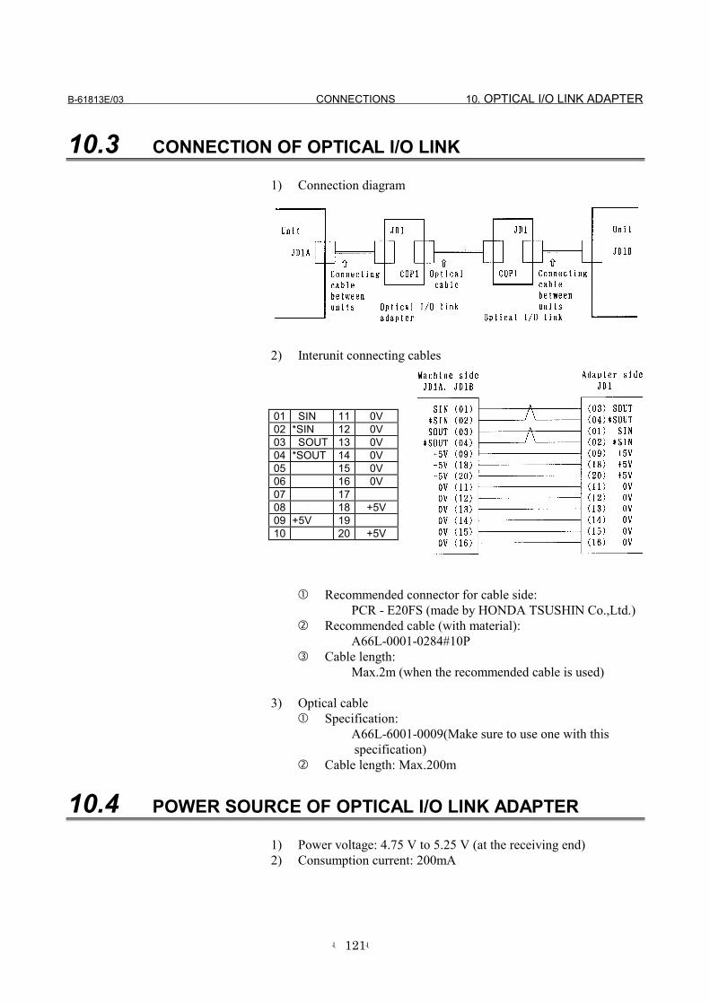
B-61813E/03 CONNECTIONS 10. OPTICAL I/O LINK ADAPTER
-121-
10.3 CONNECTION OF OPTICAL I/O LINK
1) Connection diagram
2) Interunit connecting cables
01 SIN 11 0V02 *SIN 12 0V03 SOUT 13 0V04 *SOUT 14 0V05 15 0V06 16 0V07 1708 18 +5V09 +5V 1910 20 +5V
Recommended connector for cable side:PCR - E20FS (made by HONDA TSUSHIN Co.,Ltd.)
Recommended cable (with material):A66L-0001-0284#10P
Cable length:Max.2m (when the recommended cable is used)
3) Optical cable Specification:
A66L-6001-0009(Make sure to use one with thisspecification)
Cable length: Max.200m
10.4 POWER SOURCE OF OPTICAL I/O LINK ADAPTER
1) Power voltage: 4.75 V to 5.25 V (at the receiving end)2) Consumption current: 200mA

10. OPTICAL I/O LINK ADAPTER CONNECTIONS B-61813E/03
-122-
10.5 INSTALLATION CONDITIONS OF OPTICAL I/O LINKADAPTER
1) As this adapter is not a closed type, install it in the same closedtype cabinet as used for the NC control unit.
2) Make sure to ground the case using the case fixing screw of theadapter.
3) As the adapter is light, it is not necessary to fix it with screws.However, keep it from getting contact with other circuits lest itshould be short-circuited. In addition, when fixing the adapter ina cabinet and the like, fix it with a L-type fitting using the casefixing screws (M3) of the adapter.
10.6 OPTICAL FIBER CABLE
This CNC uses optical cables for connections between the control unitand the I/O unit. Unlike the conventional power cables, optical fibercables need special care in installation and handling.
10.6.1 External view of optical fiber cable
(1) Standard length of an optical fiber cable is 5, 10, and 15 meters.
(2) An optical fiber cable cannot be cut and joined at machinemanufacturers side.
(3) If it needs to relay on cabling, use optical fiber adapter. Up to therelay points are allowed on a transmission line.
Reinforced optical fiber code diameter: 8.4mmTensile strength: Optical fiber code: 25kg
Optical fiber code-connector: 2kgReinforcing cover: 150kg
Bending radious of optical fiber code with reinforcing cover: 50mm

B-61813E/03 CONNECTIONS 10. OPTICAL I/O LINK ADAPTER
-123-
10.6.2 Notice of optical fiber cable handling
(1) Even though reinforcing cover used on the optical fiber code hasenough mechanical strength, be sure not to be damaged by heavymaterials drop.
(2) Detaching and attaching of optical connector should always bemade by touching connector. Optical fiber code should not betouched when replacement.
(3) Optical connector is automatically locked with upper side locklevels after being connected. It is impossible to pull out theconnector without releasing the lock levers.
(4) Optical connector can not be connected oppositely. Be sure theconnector direction when connection is done.
(5) Optical connector should be processed as follows before laying ofoptical fiber cable.
• Fix a reinforcing cover to a wire with hook or tensionmember by a tape.At laying hook the wire or pull the tension member takingenough care that opticalconnector does not receive pullingstrength.
(6) Reinforcing cover is fixed to cable lamp so that optical fiber cablecould not weigh directly the connecting part of connector.
(7) Notice that optical connector's chip is clear.The attached protect cap must be always put on when opticalconnector is not used.Remove dirty with a clear tissue or absorbent cotton (cotton withethyl alcohol is applicable). No other organic solvent than ethylalcohol can not be used.

10. OPTICAL I/O LINK ADAPTER CONNECTIONS B-61813E/03
-124-
10.6.3 Optical fiber cable clamping method
When reinforcing cover is fixed at cable clamp with sponge, enoughsag at optical fiber code as shown below is necessary so that connectingpart of optical should not be weighed directly by optical fiber cable.

B-61813E/03 CONNECTIONS 10. OPTICAL I/O LINK ADAPTER
-125-
10.6.4 Relay using an optical fiber adapter
(1) External view of an optical fiber adapter
(2) Example of the use of an optical fiber adapter
NOTEUp to one relay points are permitted.
10.6.5 Maximum transmission distance by optical fiber cable
Maximum transmission distance by optical fiber cable is shown below:Maximum transmission distance varies depend on numbers of relaypoints by optical fiber adapter.
Relay points Max. trans. distance (total)0 200m1 100m

11. I/O LINK DUMMY UNIT CONNECTIONS B-61813E/03
-126-
11 I/O LINK DUMMY UNIT
11.1 OVERVIEW
If a slave unit (such as the FS0, Power Mate, I/O Unit-MODEL A, orconnection unit) is removed from the FANUC I/O Link (NOTE), thegroup number for those that followed the removed slave unit changes.So, it becomes necessary to change the PMC assignment. However,connecting a FANUC I/O Link dummy unit in place of the removedslave unit makes it unnecessary to change PMC assignment.
This document describes the electrical and structural specifications thatapply to the FANUC I/O Link dummy unit when it is connected to theFANUC I/O Link.
NOTEThe FANUC I/O Link is a serial interface forconnecting the CNC or cell controller to the I/O Unit-MODEL A, Power Mate, or other units for high-speedtransfer of I/O signals (bit data).
11.2 EXTERNAL DIMENSIONS
Mounting hole for 2-M4
Units: mm
Mounting hole for 2-M5

B-61813E/03 CONNECTIONS 11. I/O LINK DUMMY UNIT
-127-
11.3 LED INDICATORS
(1) PWR: Lights when the FANUC I/O Link dummy unit is suppliedwith power.
(2) LINK: Lights when the FANUC I/O Link is performingcommunication.
11.4 WEIGHT
(1) Main unit: Approximately 120 g
11.5 POWER REQUIREMENTS
(1) Supply voltage: 4.75 to 5.25 V (at reception terminal)
(2) Required current: 180 mA (maximum)
(3) Power dissipation: 0.9 W
(4) Supply method: Via the I/O link cable
11.6 INSTALLATION CONDITIONS
This unit is not hermetically sealed. So, it must be installed in a cabinetthat is hermetically sealed to the same level as that for the NC. Thecabinet must be installed in a location where the followingenvironmental requirements are satisfied.
(1) Ambient temperatureOperating: 0 to 45°CStorage and transportation: -20 to 60°C
(2) HumidityNormal: 75% or less (relative)Short-period (within one month): 95% (maximum)
(3) VibrationOperating: 0.5 G or less

11. I/O LINK DUMMY UNIT CONNECTIONS B-61813E/03
-128-
11.7 CONNECTION DIAGRAMS
11.7.1 When not connecting FANUC I/O Link dummy units in series
Fig. 11.7.1 Example of Using the FANUC I/O Link Dummy Unit(in Place of the Power Mate)
(1) Replacing a cableThe FANUC I/O Link dummy unit is supplied with power fromthe preceding or following group via a K3X cable. So, the K1Xcable at either JD1A or JD1B of the dummy unit must be replacedwith the K3X cable ( or in Fig. 11.7.1).
CAUTIONDo not attach a K3X cable to JD1A and JD1Bsimultaneously.
(2) Cable lengthK1X cable: 10 m (maximum)K3X cable: 2 m (maximum)
CNCCell controllerJD1A
Operator's panelconnection unit
Operator's panelconnection unit
FANUC I/O Linkdummy unit
CNCCell controllerJD1A

B-61813E/03 CONNECTIONS 11. I/O LINK DUMMY UNIT
-129-
11.7.2 Connecting FANUC I/O Link dummy units in series
Fig. 11.7.2
(1) Number of FANUC I/O Link dummy units that can be used insuccessionUp to two FANUC I/O Link dummy units can be connected via aK3X cable to a unit that supplies power to them. (See Fig. 11.7.2.)
(2) Cable lengthK1X cable: 10 m (maximum)K3X cable: 2 m (maximum) in total (a + b ≤ 2 m and c + d ≤ 2 m)
11.7.3 Grounding
Ground the case of the FANUC I/O Link dummy unit.
Unit withFANUC I/OLink
FANUCI/O Linkdummyunit
FANUCI/O Linkdummyunit
FANUCI/O Linkdummyunit
FANUCI/O Linkdummyunit
Unit withFANUC I/OLink
Up to two unitsUp to two meters
Up to tenmeters
Up to two unitsUp to two meters

11. I/O LINK DUMMY UNIT CONNECTIONS B-61813E/03
-130-
11.7.4 K3X cable
• Cable connector
PinManufacturerSoldering type Crimping type
Housing
Honda Tsushin PCR-E20FS PCR-E20FA PCR-V20LAHirose Electric FI-40-20S FI-30-20S FI-20-CV2
Fujitsu - FCN-247J020-G/E FCN-240C020-Y/S
• Use twisted-pair wires for the SIN, *SIN, SOUT, and *SOUTsignals.
• Recommended wires : A66L-0001-0284#10P (twisted-pair wireswith common shielding)
• Maximum cable length : 2 m (when recommended wires are used)• Do not connect a wire to an idle pin.• Connect the cable shielding to the grounding plate of the cabinet
via a metal cable clamp at JD1A. (See the applicable CNC or cellcontroller connection manual.)
CNC, cell controller,AIF01A, etc., or FANUC I/OLink dummy unit
FANUC I/O Link dummyunit, AIF01A, or the like
Connector (see the diagrambelow.)

B-61813E/03 CONNECTIONS 12. SAFETY FOR USING AC
-131-
12 SAFETY FOR USING ACIF AC output module or AC input module is used, 12.1 is recommendedfor safety. IF 12.1 must be observed for Europe. [conforming toEN50178]

12. SAFETY FOR USING AC CONNECTIONS B-61813E/03
-132-
12.1 INSTALLATION ENVIRONMENT
12.1.1 Installation Category (Overvoltage Category)
The available impulse surge level to the ground that appears in thepower source is 2.5kV maximum.(100VAC system power source is needed in AC input moduleAccording to the standard, the available impulse surge level to theground is 1.5kV for this power source (voltage of which is 150VAC orless) However, for this module, the available impulse surge level to theground thet apperars in the power source is 2.5 kV.)Generally, an isolation transformer used for the main power source isregardrd as an effective surge filter.
The class of the 16-point relay output module (AOR16G) is set toinstallation category (overvoltage category) I.(Keep any impulse voltage to ground that may appear on the AC powerto within 1.5 kV.)The class for the 8-point relay output module (AOR08G), AC outputmodule, and AC input module is set to installation category(overvoltage category) II.
12.1.2 Pollution Degree
Install the unit in the environment of pollution degree 2 orbetter.[EN50178]In cabinet of IP-54 or better (described in 3.1), it can be considered aspollution degree 2 or better usually. The IP degree required isdependend on the circumstances of machine tool, so please chooce theadequate degree in accordance with such environment.

II. MAINTENANCE


B-61813E/03 MAINTENANCE 1. OVERVIEW
-135-
1 OVERVIEW
1.1 SYSTEM CONFIGURATION
I/O Unit-A is connected to a CNC and cell controller through a high-speed serial interface, I/O Link.
1) The I/O Link consists of a master and slaves.Master: Series 0-C, Series 15/16/18/20/21, Series
15i/16i/18i/20i/21i, Power Mate-D/H, Power Mate i-D/H and F-D Mate
Slave: I/O Unit-A, Power Mate, operator's panel connectionunit, and Series 0-C
2) One I/O Link can connect to up 16 groups of slaves. If the masteris not a CNC, one slave group can contain up to 4 of I/O Unit A (4base units). If the master is a CNC or Power Mate the number ofunits per slave group is limited to within 2.

1. OVERVIEW MAINTENANCE B-61813E/03
-136-
1.2 I/O UNIT-A CONFIGURATION
An I/O unit-A consists of a base unit, interface module, and I/Omodules.
Interface module(AIF01A , AIF01B, or AIF02C)
Interface module(AIF01A, or AIF02C) I/O modules
Base unit (ABU05A, ABU10A, ABU05B, or ABU10A)

B-61813E/03 MAINTENANCE 1. OVERVIEW
-137-
1.3 BLOCK DIAGRAM

1. OVERVIEW MAINTENANCE B-61813E/03
-138-
1.4 LIST OF UNITS
Name Arrangementdrawing No.
Unit drawingNo.
PCB drawingNo.
Horizontal type ABU10A A03B-0807-J001 A03B-0807-C001 A20B-9001-0040Base unit.10 slots Vertical type ABU10B A03B-0807-J004 A03B-0807-C004 A20B-2000-0550
or -2003-0100Horizontal type ABU05A A03B-0807-J002 A03B-0807-C002 A20B-2000-0020Base unit
5 slots Vertical type ABU05B A03B-0807-J003 A03B-0807-C003 A20B-9001-0510Interface module AIF01A A03B-0807-J011 A03B-0807-C011 A20B-8000-0410Interface module AIF01B A03B-0807-J012 A03B-0807-C012 A20B-8000-0420Interface module AIF02C A03B-0807-J013 A03B-0807-C013 A20B-8000-0710
32 points.20ms
AID32A1 A03B-0807-J101 A03B-0807-C101 A20B-9000-0970
32 points.2ms
AID32B1 A03B-0807-J102 A03B-0807-C102 A20B-9000-0971
Non-insulations
8 points.2ms24 points.20ms
AID32H1 A03B-0807-J111 A03B-0807-C111 A20B-9000-0972
16 points.NEG, 20ms
AID16C A03B-0807-J103 A03B-0807-C103 A20B-9000-0931
16 points.POS, 20ms
AID16D A03B-0807-J104 A03B-0807-C104 A20B-9000-0901
16 points.NEG, 2ms
AID16K A03B-0807-J113 A03B-0807-C113 A20B-9000-0932
16 points.POS, 2ms
AID16L A03B-0807-J114 A03B-0807-C114 A20B-9000-0902
32 points.20ms
AID32E1 A03B-0807-J105 A03B-0807-C105 A20B-9001-0010
32 points.20ms
AID32E2 A03B-0807-J110 A03B-0807-C110 A20B-9001-0280
32 points.2ms
AID32F1 A03B-0807-J106 A03B-0807-C106 A20B-9001-0011
DCinputmodule
Insulations
32 points.2ms
AID32F2 A03B-0807-J109 A03B-0807-C109 A20B-9001-0281
AC input module. 16 points AIA16G A03B-0807-J107 A03B-0807-C107 A20B-8000-0341Noninsulations
32 points.NEG
AOD32A1 A03B-0807-J162 A03B-0807-C162 A20B-9001-0110
8 points.NEG
AOD08C A03B-0807-J151 A03B-0807-C151 A20B-9001-0210or -9000-0951
DCoutputmodule Insulations
8 points.POS
AOD08D A03B-0807-J152 A03B-0807-C152 A20B-9001-0220or -9000-0911

B-61813E/03 MAINTENANCE 1. OVERVIEW
-139-
Name Arrangementdrawing No.
Unit drawingNo.
PCB drawingNo.
16 points.NEG
AOD16C A03B-0807-J153 A03B-0807-C153 A20B-9000-0941
16 points.POS
AOD16D A03B-0807-J154 A03B-0807-C154 A20B-9000-0921
32 points.NEG
AOD32C1 A03B-0807-J155 A03B-0807-C155 A20B-9001-0070
32 points.NEG
AOD32C2 A03B-0807-J172 A03B-0807-C172 A20B-9001-0530
32 points.POS
AOD32D1 A03B-0807-J156 A03B-0807-C156 A20B-8000-0440
DCoutputmodule
Insulations
32 points.POS
AOD32D2 A03B-0807-J167 A03B-0807-C167 A20B-8000-0510
5 points.2A
AOA05E A03B-0807-J157 A03B-0807-C157 A20B-8000-0470or -8000-0251
8 points.1A
AOA08E A03B-0807-J158 A03B-0807-C158 A20B-8000-0480or -8000-0381
AC output module
12 points.0.5A
AOA12F A03B-0807-J159 A03B-0807-C159 A20B-8000-0321
8 points.4A
AOR08G A03B-0807-J160 A03B-0807-C160 A20B-9001-0200or -9000-0961
16 points.2A
AOR16G A03B-0807-J161 A03B-0807-C161 A20B-8000-0101
Relay output module
16 points.2A
AOR16H2 A03B-0807-J165 A03B-0807-C165 A20B-8000-0500
Analog input module AAD04A A03B-0807-J051 A03B-0807-C051 A20B-8000-0450Analog output module (12-bit) ADA02A A03B-0807-J052 A03B-0807-C052 A20B-8000-0460Analog output module (14-bit) ADA02B A03B-0807-J060 A03B-0807-C060 A20B-8001-0980High speed counter module ACT01A A03B-0807-J053 A03B-0807-C053 A20B-8000-0540
Pt/Pt AT104A A03B-0807-J056 A03B-0807-C056 A74L-0001-0083#PtTempereture input moduleJ/K AT104B A03B-0807-J057 A03B-0807-C057 A74L-0001-0083#JKPt/Pt ATB01A A03B-0807-J350 A03B-0807-C350 A20B-1005-0920Relay terminal unitJ/K ATB01B A03B-0807-J351 A03B-0807-C351 A20B-1005-0930
Optical adapter A13B-0154-B0001 - A20B-1004-0240Dummy unit A13B-0167-B0001 - A20B-8000-0940

2. INDICATION MAINTENANCE B-61813E/03
-140-
2 INDICATIONThe interface modules and the I/O modules with up to 16 input/outputpoints have LEDs toindicate their states.
2.1 INTERFACE MODULE (AIF01A) LEDS
PWR LINK
BA1
BA0
A I F 0 1 A
Marking Name DescriptionPWR Power-on On: The interface module is supplied with power
of 24 VDC.LINK Link On: The I/O Link is operating properly.
Normally, this LED lights several to ten-oddseconds after the master is turned on.
BA1BA0
Base address These LEDs indicate which base unit the inter-facemodule is transferring data with. If a failure occurs(the LINK LED is turned on, then off), BA0 or BA1,whichever is operating, is turned on.
Failures, their causes, and required actions
1) PWR is off.
Power (24 VDC) is not supplied or the supply voltage isabnormal.
Supply power of 24 VDC ± 10%.
A The fuse in the interface module has blown.
BA1 BA0 Base number
Base #0 : Off
Base #1 : On
Base #2
Base #3
B-61813E/03 MAINTENANCE 2. INDICATION
-141-
Eliminate the cause that made the fuse to blow, thenreplace the fuse with a spare. (See Section 3.) Thefollowing may cause the fuse to blow:
• A sum of power requirements for all input modulesexceeds the rating. (Refer to I-4.4)
• A voltage of +24 VDC, supplied from input moduleAID32A1, AID32B1 or AID32H1 to the outside, isshort-circuited to the cabinet or the like.
• The interface module or any of the I/O modules isdefective.
An I/O module is defective.
Remove the I/O modules sequentially to pinpoint thedefective one. Then, eplace it with a spare.
An interface module is defective.
Replace it with a spare.
2) LINK has never been turned on since power is supplied.
If PWR is off, go to item 1).
The attempted power turn-on sequence was incorrect.
The slaves (I/O Unit-A, Power Mate, Series 0, etc.)must be supplied with power at the same time orbefore the master (CNC or F-D Mate) is suppliedwithpower. (Refer to I-4.2)If an attempt is made to supply power to a slave on aninterface module after the master isurned on, LINK onthe interface module is not turned on provided that theinterface module corresponds to that slave or to anyslave ahead of that slave (one on the far side withrespect to the master).
I/O Link cables are broken or short-circuited.
With reference to Note below, check the cables, andtake an appropriate action.

2. INDICATION MAINTENANCE B-61813E/03
-142-
Any device on the I/O Link is defective.
With reference to Note below, find a defective device,and take an appropriateaction. If an I/O unit seems tobe defective, replace interface module AIF01Awith aspare.
NOTEHow to pinpoint a failure in the I/O Link in event ofitems to .
Check the LEDs on the master to find out which groupcontains slaves whose I/OLink is established with themaster. (Refer to the maintenance manual forthemaster.)
For example, if the master is linked to slaves (slave #0and #1) that belong to separate groups, the timing ofturning on slave #2 is bad, the cable is broken or short-circuited at point (a), slave #2 is defective.
If the master is not linked to any slave, the master maybe defective.
3) LINK is turned on once, then off.
One of the devices on the I/O Link is turned off.
Turn off all devices, then turn them on.
The DI/DO assignment for the master is invalid.
When I/O unit bases 1 to 3 (units under control ofinterface module AIF01B) are not connected, if DI/DOunits are assigned to these bases, LINK is turned on, butturned off immediately.Correct the DI/DO assignment.

B-61813E/03 MAINTENANCE 2. INDICATION
-143-
The I/O Link cable is broken or short-circuited.
Check the cable, and take an appropriate action. Any device on the I/O Link is defective.
With reference to the maintenance manual for themaster, find a defective device, and take an appropriateaction. If an I/O unit seems defective,replace the interface module (AIF01A or AIF01B)installed in the base unit indicated by BA1 or BA0.

2. INDICATION MAINTENANCE B-61813E/03
-144-
2.2 INTERFACE MODULE (AIF01B) LEDS
PWR LINK
A I F 0 1 B
Marking Name DescriptionPWR Power-on On: The interface module is supplied with power of
24 VDC.LINK Link On: The I/O Link is operating properly.
Normally, this LED lights several to ten-odd seconds after the master is turned on.
Failures, their causes, and required actions
1) PWR is off.
Power (24 VDC) is not supplied or the supply voltage isabnormal. Supply power of 24 VDC ±10%.
The fuse in the interface module has blown.
Eliminate the cause that made the fuse to blow, thenreplace the fuse with a spare. (See Chapter 3.) Thefollowing may cause the fuse to blow:
• A sum of power requirements for all input modulesexceeds the rating. (Refer to I-4.4)
• A voltage of +24 VDC, supplied from input moduleAID32A1, AID32B1 or AID32H1 to the outside, isshort-circuited to the cabinet or the like.
• The interface module or any of the I/O modules isdefective.
An I/O module is defective.
Remove the I/O modules sequentially to pinpoint thedefective one. Then, replace it with a spare.

B-61813E/03 MAINTENANCE 2. INDICATION
-145-
An interface module is defective.
Replace it with a spare.
2) LINK has never been turned on since power is supplied.
If PWR is off, go to item 1).
If LINK on the AIF01A in the same group is off, go toSection 2.1.
The signal cable between I/O units in the same group isbroken or short-circuited.
Check the cable, and take an appropriate action.
An interface module is defective.
Replace it with a spare.
3) LINK is turned on once, then turned off.
See section 2.1.

2. INDICATION MAINTENANCE B-61813E/03
-146-
2.3 INTERFACE MODULE (AIF02C) LED INDICATORS
The LED indicator panel of the AIF02C is shown below. Each of itscomponents are described in the following paragraphs.
2.3.1 PWR indicator
This LED lights when the power is switched on.
2.3.2 LNK indicators
(1) LNK-1 : Lights when the I/O link for the I/O Unit-A is operatingnormally.
(2) LNK-2 : Lights when the I/O link for the I/O Unit-B is operatingnormally.
(3) LNK-D : Lights when the distributed link with the I/O Unit-B isoperating normally. (The indicator dims if only a fewbase units are connected.)
2.3.3 ER indicators
An ER indicator lights if an error occurs on the distributed link.
See the tables on the following page for details.
2.3.4 LED indicators
(1) When the unit No. (1 to 16) is off (o-on and ×-off)
M/S ER2 ER1 ER0 Error Description Major cause of error × × Interface unit peripheral error The interface unit is abnormal. Interface unit failure × × Interface unit RAM parity error The interface unit is abnormal. Interface unit failure × × I/O link error reception An error has occurred in a unit
connected to the I/O link.Failure in a unit connected tothe I/O link
× I/O link framing error The I/O link communicationend signal is abnormal.
-
× I/O link CRC error I/O link communication data isabnormal.
-
Interface unit watchdog timererror
Communication from the I/Olink host has stopped.
-
M
LNK

B-61813E/03 MAINTENANCE 2. INDICATION
-147-
(2) When the unit No. (1 to 16) is on (o-on and ×-off)
M/S ER2 ER1 ER0 Error Description Major cause of error× × × Basic unit peripheral error The basic unit is abnormal. Basic unit failure × × Basic unit number error A unit with an invalid unit
number has responded to theinterface unit.
-
× × Basic unit reception data counterror
The number of communicationbytes has exceeded four.
Two or more units have thesame unit number, or the unitof interest is not provided with aterminating resistor.
×(*1)
× × Basic unit framing error The communication end signalis abnormal.
Two or more units have thesame unit number, or the unitof interest is not provided with aterminating resistor.
×(*1)
× Basic unit DMI error The communication waveformhas been distorted.
Two or more units have thesame unit number, or the unitof interest is not provided with aterminating resistor.
×(*1)
× Basic unit CRC error The communication data isabnormal.
Two or more units have thesame unit number, or the unitof interest is not provided with aterminating resistor.
× Basic unit watchdog timer error Communication with theinterface unit has stopped.
-
NOTE (*1)If M/S lights, it means that the interface detected theerror.
If it does not light, it means that the basic unit detectedthe error.
2.3.5 M/S indicator
If an error occurs on a distributed link, the M/S indicator indicateswhether the error was detected in the interface module or basic errorside.
On: The error has been detected on the interface module side.Off: The error has been detected on the basic unit side.

2. INDICATION MAINTENANCE B-61813E/03
-148-
2.3.6 No. Indicators
If an error occurs on a distributed link, the No. indicators indicate thebasic unit No. where the error is detected. The sum of the values forwhich a lamp lights corresponds to the basic unit No.
Example)No.
16 8 4 2 1 Unit No.× × × × 1 -On× × × 5 ×-Off× × × 10 × × × 20
2.4 LED INDICATORS ON THE INPUT/OUTPUT MODULES(HAVING 16 OR FEWER INPUT/OUTPUT POINTS)
A01234567F
B01234567
Label Name DescriptionA0 to 7B0 to 7
Input/outputindicator
On : The corresponding input or output ison.
F Fuse alarm On : A fuse incorporated in the outputmodule has blown.

B-61813E/03 MAINTENANCE 3. FUSES
-149-
3 FUSESThe modules listed below have built-in fuses. If a fuse blows, removethe cause, then replace the fuse with a spare.
Module Indication Rating Fuse specificationInterface module AIF01A PWR is off 3.2A A60L-0001-0290#LM32Interface module AIF01B PWR is off. 3.2A A60L-0001-0290#LM32Interface module AIF02C PWR is off. 3.2A A60L-0001-0290#LM32Output module with 8 DC points AOD08C F is on. 5A A60L-0001-0260#5R00Output module with 8 DC points AOD08D F is on. 5A A60L-0001-0260#5R00Output module with 5 AC points AOA05E F is on. 3.15A A60L-0001-0276#3.15Output module with 8 AC points AOA08E F is on. 3.15A A60L-0001-0276#3.15Output module with 12 AC points AOA12F F is on. 3.15A A60L-0001-0276#3.15
The fuses are on the PC boards in the modules.

4 REMOVING PC BOARDS MAINTENANCE B-61813E/03
-150-
4 REMOVING PC BOARDS
4.1 HOW TO REMOVE TERMINAL BOARD-TYPE I/O MODULEPC BOARDS
Remove the terminal board. (Refer to I-4.5)
Pull the LED cap in the direction of the arrow to remove it.
While pressing connector in the direction of the arrow, raise thetabs (two) on the module case with a flat-blade screwdriver.

B-61813E/03 MAINTENANCE 4. REMOVING PC BOARDS
-151-
Put the tip of a flat-blade screwdriver into the gap between themodule case and terminal board connector, as shown below.While pressing the screwdriver in the direction of arrow A, pushconnector in the direction of arrow B, and the PC board willcome out.

4 REMOVING PC BOARDS MAINTENANCE B-61813E/03
-152-
4.2 HOW TO REMOVE INTERFACE AND CONNECTOR-TYPEI/O MODULE PC BOARDS
While pulling the cover in the direction of the arrow, press points and (on each side) with a flat-blade screwdriver to removethe cover.
Pull the LED cap in the direction of the arrow to remove it.
While pressing connector in the direction of the arrow, raise thetabs (two for a connector type I/O module and 4 for an interfacemodule) with a flat-screwdriver, then push connector in thedirection of the arrow, and e PC boardwill come out.
Cover
LED Cap

B-61813E/03
i-1
INDEX12
12-BIT ANALOG OUTPUT MODULE (ADA02A) 65
AALLOCATION OF I/O POINTS 5
ANALOG INPUT MODULE (AAD04A) 61
ANALOG OUTPUT MODULE 65
BBLOCK DIAGRAM 137
CComparison function 72
COMPLETE CONNECTION OF TEMPERATUREINPUT MODULE 107
Configuration of mode A 93
CONFIGURATION 4
Connecting FANUC I/O Link dummy units in series129
CONNECTING INPUT POWER SOURCE 15
CONNECTING WITH ANALOG INPUT MODULE64
CONNECTING WITH I/O MODULES 25
Connection between the Analog Output Module andLoad 69
Connection diagram 86
CONNECTION DIAGRAMS 128
CONNECTION OF OPTICAL I/O LINK 121
Connection to Analog Output Module 67
CONNECTION WITH POWER MAGNETICSCABINET 90
CONNECTION WITH PULSE GENERATOR 88
CONNECTION 14
Connection 22
Connector signal list 87
Connector signal lists 108
CORRESPONDENCE BETWEEN I/O SIGNALSAND ADDRESSES IN A MODULE 29
CORRESPONDENCE BETWEEN INPUT SIGNALSAND ADDRESSES IN A MODULE 62
Correspondence between Output Signals and Addressesin a Module 66
Correspondence between Output Signals and Addressesin the Module 68
Counter presetting and counting 94
DDC input signals (ME and CSP) 92
DESIGNING CONDITION FOR A CABINET 10
Details of input signals (temperature module → PMC)104
Details of output signals (PMC → temperature module)102
Details of PMC interface signals 83
DIGITAL INPUT / OUTPUT MODULES 27
EENVIRONMENTAL CONDITIONS 9
ER indicators 146
External contact input 76
External contact output 76
EXTERNAL DIMENSION OF OPTICAL I/O LINK120
EXTERNAL DIMENSIONS 126
External view of optical fiber cable 122
FFANUC I/O LINK 3
FOURTEEN-BIT ANALOG OUTPUT MODULE(ADA02B) 68
FUSES 149
GGENERAL CONNECTION DIAGRAM 14
Grounding 129
GROUNDING 16
HHIGH SPEED COUNTER MODULE 70
HOW TO REMOVE INTERFACE ANDCONNECTOR-TYPE I/O MODULE PC BOARDS152
HOW TO REMOVE TERMINAL BOARD-TYPE I/OMODULE PC BOARDS 150

INDEX B-61813E/03
i-2
II/O LINK DUMMY UNIT 126
I/O SIGNALS CONVENTIONS 91
I/O UNIT CONFIGURATION 8
I/O UNIT-A CONFIGURATION 136
INDICATION 140
Installation Category (Overvoltage Category) 132
INSTALLATION CONDITIONS OF OPTICAL I/OLINK ADAPTER 122
INSTALLATION CONDITIONS 127
INSTALLATION ENVIRONMENT 132
INSTALLATION 9
INTERFACE MODULE (AIF01A) LEDS 140
INTERFACE MODULE (AIF01A, AIF01B) 18
INTERFACE MODULE (AIF01B) LEDS 144
INTERFACE MODULE (AIF02C) CONNECTION 21
INTERFACE MODULE (AIF02C) LEDINDICATORS 146
KK3X cable 130
LLED INDICATORS ON THE INPUT/OUTPUTMODULES (HAVING 16 OR FEWERINPUT/OUTPUT POINTS) 148
LED INDICATORS 127
LED indicators 146
LED Indicators 77
LIST OF MODULES 27
LIST OF UNITS 138
LNK indicators 146
MM/S indicator 147
Marker processing 76
Maximum transmission distance by optical fiber cable125
MEASUREMENT EXAMPLES 111
Measurement mode 102
Miscellaneous information 98
Mode A 79
Mode B 81
MOUNTING AND DISMOUNTING MODULES 13
NNo. Indicators 148
Notice of optical fiber cable handling 123
OOptical fiber cable clamping method 124
OPTICAL FIBER CABLE 122
OPTICAL I/O LINK ADAPTER 119
OUTER DIMENSION OF I/O Unit 11
OUTLINE OF HIGH SPEED COUNTER MODULE70
Overview 21
OVERVIEW 99
OVERVIEW 135
OVERVIW 126
PPMC I/O area 101
PMC INTERFACE 101
PMC INTERFACE 79
Pollution Degree 132
POWER REQUIREMENTS 127
POWER SOURCE OF OPTICAL I/O LINKADAPTER 121
Pulse counter 72
Pulse Interface 74
PWR indicator 146
RReading data 97
Relay using an optical fiber adapter 125
REMOVING PC BOARDS 150
REQUIRED CURRENT 17

B-61813E/03 INDEX
i-3
SSAFETY FOR USING AC 131
Setting data 95
Setting with the DIP switch 24
Solid state relay output signals (OUT0 to OUT7) 91
SPECIFICATION FOR EACH MODULE 30
Specification 65
Specification 68
SPECIFICATIONS FOR ANALOG INPUT MODULE61
SPECIFICATIONS OF HIGH SPEED COUNTERMODULE 72
SUPPLEMENT 93
SYSTEM CONFIGURATION 135
TTemperature input module connection diagram 107
TEMPERATURE INPUT MODULESPECIFICATION 100
TEMPERATURE INPUT MODULE 99
TERMINAL BOARD UNIT DIMENSIONS 118
Terminal board unit connection diagram 109
TIMING CHARTS 110
TOTAL CONNECTION OF HIGH SPEEDCOUNTER MODULE 86
UUse of phase A and B pulses 88
Use of positive/negative pulses 89
WWEIGHT OF OPTICAL I/O LINK 120
WEIGHT 127
When not connecting FANUC I/O Link dummy units inseries 128

Rev
isio
n R
ecor
d
FAN
UC
I/O
Uni
t-MO
DEL
A C
ON
NEC
TIO
N·M
AIN
TEN
ANC
E M
ANU
AL (B
-618
13E/
03)
03Fe
b.,2
000
A
dditi
on o
f “I/O
Lin
k du
mm
y un
it” A
dditi
on o
f Int
er fa
ce m
odul
e (A
IF02
C)
A
dditi
on o
f Inp
ut m
odul
e (A
ID16
K, A
ID16
L) A
dditi
on o
f Hig
h-re
solu
tion
type
ana
log
outp
utm
odul
e (A
DA
02B
) A
dditi
on o
f “Te
mpe
ratu
re in
put m
odul
e” M
odifi
catio
n of
“H
igh
spee
d co
unte
r m
odul
e”
02Ap
r.,19
92 A
dditi
on o
f hig
h sp
eed
coun
ter
mod
ule
A
dditi
on o
f Opt
ical
fibe
r C
able
01De
c.,1
990
Edi
tion
Dat
eC
onte
nts
Edi
tion
Dat
eC
onte
nts

EUROPEAN HEADQUARTERS –GRAND-DUCHÉ DE LUXEMBOURG
GE Fanuc Automation Europe S.A.Zone Industrielle
L-6468 Echternach (+352) 727979 - 1 (+352) 727979 - 214
BELGIUM / NETHERLANDSGE Fanuc Automation Europe S.A.
- Netherlands Branch -Postbus 7230 - NL-4800 GE Breda
Minervum 1603A - NL-4817 ZL Breda (+31) 76-5783 201 (CNC) (+31) 76-5783 212 (PLC)
(+31) 76-5870 181CZECH REPUBLIC
GE Fanuc Automation CR s.r.o.U studanky 3
CZ-170 00 Praha 7 (+420) 2 333 72 502 (CNC) (+420) 2 333 72 503 (PLC)
(+420) 2 333 70 821
FRANCEGE Fanuc Automation France S.A.
39, rue du Saule Trapu, BP 219F-91882 Massy Cedex
(+33) 1 69 75 86 39 (CNC) (+33) 1 69 75 86 20 (PLC)
(+33) 1 69 75 86 49
GERMANYGE Fanuc Automation GmbH
Bernhäuser Straße 22D-73765 Neuhausen a.d.F
(+49) 7158 187 400 (+49) 7158 187 455 (CNC) (+49) 7158 187 466 (PLC)
GERMANYGE Fanuc Eberle Automation GmbH
Ernst-Weyden-Str. 7D-51105 Köln (Cologne) (+49) 221-83904-53 (+49) 221-83904-55
GERMANYGE Fanuc Automation GmbH
Elberfelderstr. 45D-40724 Hilden
(+49) 2103 247410 (Laser/CNC) (+49) 2103 247420 (Laser/CNC)
GERMANYGE Fanuc Automation GmbH
Obere Hauptstr. 72D-09244 Lichtenau
(+49) 37208 695 20(CNC) (+49) 37208 695 30 (PLC)
(+49) 37208 695 55GERMANY
GE Fanuc Automation Deutschland GmbHBensheimer Str. 61
D-65428 Rüsselsheim (+49) 6142 357600 (+49) 6142 357611
GERMANYGE Fanuc Eberle Automation GmbH
Südwestpark 48D-90449 Nürnberg
(+49) 911 9672 100 (PLC) (+49) 911 9672 200 (PLC)
GERMANYGE Fanuc Eberle Automation GmbH
Reichenbergerstr. 6D-33605 Bielefeld
(+49) 521 92445 0 (PLC) (+49) 521 92445 30 (PLC)
SWEDENGE Fanuc Automation Nordic AB
Hammarbacken 4S-19149 Sollentuna (+46) 8 444 5520 (+46) 8 444 5521
ITALYGE Fanuc Automation Italia S.r.l.
Piazza Tirana 24/4BI-20147 Milano
(+39) 02 417 176 (CNC) (+39) 02 419 669 (CNC)
ITALYGE Power Controls Italia S.p.a
Via Tortona 27I-20144 Milano
(+39) 02 4242 280 (PLC) (+39) 02 4242 511 (PLC)
SPAINGE Fanuc Automation España S.A.
Polígono Industrial OlasoCalle Olaso, 57 - Locales 10 y 11
E-20870 Elgoibar (+34) 943 74 82 90 (CNC) (+34) 943 74 44 21 (CNC)
SPAINGE Power Controls Ibérica S.L.Calle Marqués de Comillas, 1E-08225 Terrassa (Barcelona) (+34) 93 736 58 28 (PLC) (+34) 93 788 24 03 (PLC)
SWITZERLANDGE Fanuc Automation
Filiale Suisse/Niederlassung SchweizErlenstrasse 35a
CH-2555 Brügg b. Biel (+41) 32 366 63 63 (CNC) (+41) 32 366 63 33 (PLC) (+41) 32 366 63 64 (CNC) (+41) 32 366 63 34 (PLC)
UNITED KINGDOMGE Fanuc Automation (UK) Ltd.
Unit 1 - Mill SquareFeatherstone RoadWolverton Mill South
Milton Keynes MK12 5BZ (+44) 1908 84 4000 (+44) 1908 84 4001
06/00


• No part of this manual may be reproduced in any form.• All specifications and designs are subject to change without prior notice.
The export of this product is subject to the authorization of the government of thecountry from where the product is exported.
In this manual we have tried as much as possible to describe all the variousmatters.However, we cannot describe all the matters which must not be done, or whichcannot be done, because there are so many possibilities.Therefore, matters which are not especially described as possible in this manualshould be regarded as “impossible”.


![1 $SU VW (G +LWDFKL +HDOWKFDUH %XVLQHVV 8QLW 1 X ñ 1 … · 2020. 5. 26. · 1 1 1 1 1 x 1 1 , x _ y ] 1 1 1 1 1 1 ¢ 1 1 1 1 1 1 1 1 1 1 1 1 1 1 1 1 1 1 1 1 1 1 1 1 1 1 1 1 1 1](https://static.documents.pub/doc/80x56/5fbfc0fcc822f24c4706936b/1-su-vw-g-lwdfkl-hdowkfduh-xvlqhvv-8qlw-1-x-1-2020-5-26-1-1-1-1-1-x.jpg)