ADJUSTABLE-SPEED SINGLE-PHASE FULL-WAVE PRE-DRIVER FOR MOTOR AM4967 Data Sheet 1 Oct. 2008 Rev. 1. 2 BCD Semiconductor Manufacturing Limited General Description The AM4967 is a single-coil, single-phase motor pre- driver designed by bipolar process. Its rotation speed can be controlled through an external PWM. This IC requires few external components and has the merit of high efficiency which make it suitable for use in great air volume, large current and high voltage applications. The AM4967 is available in SSOP-16 package. Features · Single-phase Full-wave Pre-drive · Rotation Speed Control via External PWM · Maximum Operating Current Limit · Linear Start Function for Reducing Large Current Impulse at the Moment of Turn-on · Minimum Rotation Speed Setting · Lock Protection and Auto Start Function · Rotation Speed Indication · Over Temperature Protection Application · CPU and OA (Office Automation) Cooler Fan · Brushless DC Motor Figure 1. Package Type of AM4967 SSOP-16
Transcript
ADJUSTABLE-SPEED SINGLE-PHASE FULL-WAVE PRE-DRIVER FOR MOTOR AM4967
The AM4967 is a single-coil, single-phase motor pre-driver designed by bipolar process. Its rotation speedcan be controlled through an external PWM. This ICrequires few external components and has the merit ofhigh efficiency which make it suitable for use in greatair volume, large current and high voltage applications. The AM4967 is available in SSOP-16 package.
Features
· Single-phase Full-wave Pre-drive· Rotation Speed Control via External PWM· Maximum Operating Current Limit· Linear Start Function for Reducing Large Current
Impulse at the Moment of Turn-on · Minimum Rotation Speed Setting· Lock Protection and Auto Start Function· Rotation Speed Indication· Over Temperature Protection
Application
· CPU and OA (Office Automation) Cooler Fan· Brushless DC Motor
Figure 1. Package Type of AM4967
SSOP-16
ADJUSTABLE-SPEED SINGLE-PHASE FULL-WAVE PRE-DRIVER FOR MOTOR AM4967
ADJUSTABLE-SPEED SINGLE-PHASE FULL-WAVE PRE-DRIVER FOR MOTOR AM4967
Oct. 2008 Rev. 1. 2
Data Sheet
Pin Number Pin Name Function
1 OUT2 Second channel P-type driver output. Open-drain output, must be connectedwith pull-up resistor to drive external power devices in operation
2 OUT2B Second channel N-type driver output. Push-pull output to drive externalpower devices
3 VCC Power supply
4 CS
Current limiter indicator. Fixed to 0.2V internally. Maximum allowable cur-rent is decided by external sample resistance. When the voltage of this pinexceeds 0.2V, the output will be shut down by current limit. If this function isnot used, connect this pin to ground directly
5 VMIN Minimum speed setting terminal. Connect it to VREF when disused. In case itis tied to other power supply for controlling, an isolated resistor is necessary
6 VPWM
Speed control terminal. It is full speed mode when connected to ground. If thespeed is controlled by PWM mode, the frequency of control signal is 20kHzto 100kHz. Moreover, a low pass network is necessary to transfer PWM toDC level
7 COSC PWM basic oscillation frequency generator when connected with a capacitorof 220pF. 30kHz frequency is available.
8 FG/RD
"FG" means pin 8 is an output pin of FG signal which is used for detectingrotation speed. "RD" means pin 8 is an output pin of RD signal, and is usedfor detecting fan rotate-stop state. "FG" and "RD" can be selected accordingto the requirement. This pin need to be connected with pull-up resistor whenused. A new pulse will be generated once input signal changed. Keep this pinopen when it is not to be used
9 HIN-Hall sensor negative input. To prevent noise, this pin is recommended to beplaced as close as possible to Hall circuit. If necessary, a capacitor may beadded between HIN+ and HIN- to reduce the influence caused by noise
10 HIN+ Hall sensor positive input. To avoid noise, this pin is recommended to beplaced as close as possible to Hall circuit
11 CTLock protection and auto start frequency generator. It is connected with an external 0.47µF capacitor which decides lock-rotate time and start time. If lock-rotate protection function is disused, please connect this pin to GND
12 LSLinear start terminal. This pin is connected to VREF externally via a capacitorof 0.47µF to 1µF which enables fan start steadily. Start time is dependent tothe capacitance. If linear start function is not used, connect this pin to ground
13 VREF 5V voltage reference
14 GND Ground for circuit control
15 OUT1B First channel N-type driver output. Push-pull output to drive external powerdevices
16 OUT1 First channel P-type driver output. Open-drain output, must be connected withpull-up resistor to drive external power devices in operation
Pin Description
ADJUSTABLE-SPEED SINGLE-PHASE FULL-WAVE PRE-DRIVER FOR MOTOR AM4967
1. Driver-lock. VOSC is High, VPWM, VVMIN and VLS are low.
R: RDBlank: FG
Pin 8
2. Speed control. VCT, VLS are low.
G1: Green
BCD Semiconductor's Pb-free products, as designated with "E1" suffix in the part number, are RoHS compliant. Products with"G1" suffix are available in green package.
ADJUSTABLE-SPEED SINGLE-PHASE FULL-WAVE PRE-DRIVER FOR MOTOR AM4967
Note 1: Stresses greater than those listed under "Absolute Maximum Ratings" may cause permanent damage to the device.These are stress ratings only, and functional operation of the device at these or any other conditions beyond those indicatedunder "Recommended Operating Conditions" is not implied. Exposure to "Absolute Maximum Ratings" for extended periodsmay affect device reliability.Note 2: When mounted on the specified printed circuit board (114.3mm×76.1mm×1.6mm, glass epoxy).
Parameter Symbol Min Typ Max Unit
Supply Voltage VCC 5.5 16 V
VPWM/VMIN Input Voltage 0 5 V
Hall Input Voltage 0.2 3 V
Ambient Temperature TA -30 105 oC
Recommended Operating Conditions
Absolute Maximum Ratings (Note 1)
7
BCD Semiconductor Manufacturing Limited
ADJUSTABLE-SPEED SINGLE-PHASE FULL-WAVE PRE-DRIVER FOR MOTOR AM4967
Oct. 2008 Rev. 1. 2
Data Sheet
Parameter Symbol Conditions Min Typ Max Unit
Quiescent Current IQ1 Lock off 8 10 12
mA IQ2 Lock on 8 10 12
VREF Reference Voltage VREF IOUT=5mA 4.5 5.0 5.5 V
Current Limit Voltage VLIM 186 200 215 mV
COSC High Level Voltage VOSCH 3.0 3.4 3.8 V
COSC Low Level Voltage VOSCL 0.9 1.1 1.3 V
COSC Frequency fOSC CL=220pF 25.4 30 35.5 kHz
CT High Level Voltage VCTH 2.4 3.3 3.6 V
CT Low Level Voltage VCTL 1.0 1.3 1.6 V
CT Charge Current ICHG VCT=0.5V 1.5 2 2.5 µA
CT Discharge Current IDHG VCT=3.5V 0.13 0.2 0.25 µA
CT Charge and Discharge Ratio RCD ICHG/IDHG 8.5 10 14.5
Linear Start Charge Current ILS VLS=1V 0.5 0.7 µA
OUT1B/OUT2B High Level Voltage VOBH IOUT=10mA VCC-
1.8VCC-0.9
VCC V
OUT1B/OUT2B Low Level Voltage VOBL IOUT=10mA 0.9 1.5 V
OUT1/OUT2 Low Level Voltage VOL IOUT=10mA 0.45 0.8 V
FG Signal Hall Input Sensitivity VHN IHIN+, IHIN- difference voltage(include offset and hysteresis)
±10 mV
FG Saturation Voltage VSAT ISINK=5mA 200 500 mV
FG Leakage Current ILFG VFG=VCC 30 µA
VPWM/VMIN Bias Current IPWMB/IVMINB VOSC=VPWM/VVMIN=2V 0.1 3 µA
(VCC=12V, TA=25oC, unless otherwise specified.)
Electrical Characteristics
ADJUSTABLE-SPEED SINGLE-PHASE FULL-WAVE PRE-DRIVER FOR MOTOR AM4967
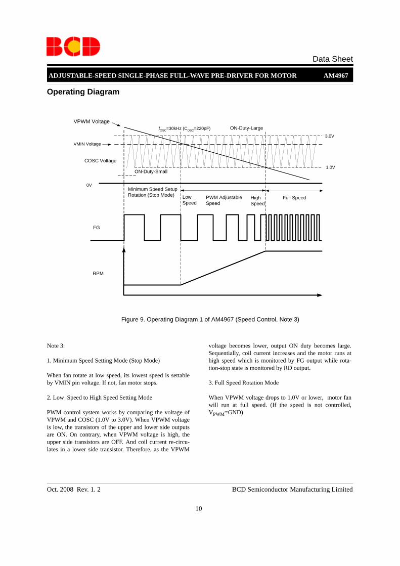
When fan rotate at low speed, its lowest speed is settableby VMIN pin voltage. If not, fan motor stops. 2. Low Speed to High Speed Setting Mode
PWM control system works by comparing the voltage ofVPWM and COSC (1.0V to 3.0V). When VPWM voltageis low, the transistors of the upper and lower side outputsare ON. On contrary, when VPWM voltage is high, theupper side transistors are OFF. And coil current re-circu-lates in a lower side transistor. Therefore, as the VPWM
voltage becomes lower, output ON duty becomes large.Sequentially, coil current increases and the motor runs athigh speed which is monitored by FG output while rota-tion-stop state is monitored by RD output.
3. Full Speed Rotation Mode
When VPWM voltage drops to 1.0V or lower, motor fanwill run at full speed. (If the speed is not controlled,VPWM=GND)
BCD Semiconductor Manufacturing Limited reserves the right to make changes without further notice to any products or specifi-cations herein. BCD Semiconductor Manufacturing Limited does not assume any responsibility for use of any its products for anyparticular purpose, nor does BCD Semiconductor Manufacturing Limited assume any liability arising out of the application or useof any its products or circuits. BCD Semiconductor Manufacturing Limited does not convey any license under its patent rights orother rights nor the rights of others.
- IC Design GroupAdvanced Analog Circuits (Shanghai) Corporation8F, Zone B, 900, Yi Shan Road, Shanghai 200233, ChinaTel: +86-21-6495 9539, Fax: +86-21-6485 9673
BCD Semiconductor Manufacturing Limited
http://www.bcdsemi.com
BCD Semiconductor Manufacturing Limited
IMPORTANT NOTICE
BCD Semiconductor Manufacturing Limited reserves the right to make changes without further notice to any products or specifi-cations herein. BCD Semiconductor Manufacturing Limited does not assume any responsibility for use of any its products for anyparticular purpose, nor does BCD Semiconductor Manufacturing Limited assume any liability arising out of the application or useof any its products or circuits. BCD Semiconductor Manufacturing Limited does not convey any license under its patent rights orother rights nor the rights of others.