104
CS4210 Geode CS4210 IEEE 1394 OHCI Controller Literature Number: SNOS923A

CS4210
Geode CS4210 IEEE 1394 OHCI Controller
Literature Number: SNOS923A
© 2000 National Semiconductor Corporation www.national.com
Geo
de™
CS
4210IE
EE
1394O
HC
ICo
ntro
ller
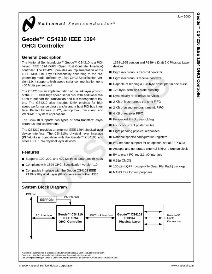
General DescriptionThe National Semiconductor® Geode™ CS4210 is a PCI-based IEEE 1394 OHCI (Open Host Controller Interface)controller. The CS4210 provides an implementation of theIEEE 1394 Link Layer functionality according to the pro-gramming model defined by 1394 OHCI Specification Ver-sion 1.0. It supports high speed serial communication up to400 Mbits per second.
The CS4210 is an implementation of the link layer protocolof the IEEE 1394 high speed serial bus, with additional fea-tures to support the transaction and bus management lay-ers. The CS4210 also includes DMA engines for highspeed performance data transfer and a host PCI bus inter-face. Perfect for use in PC, set-top box, thin client, andWebPAD™ system applications.
The CS4210 supports two types of data transfers: asyn-chronous and isochronous.
The CS4210 provides an external IEEE 1394 physical layerdevice interface. The CS4210’s physical layer interface(PHY-Link) is compatible with the Geode™ CS4103 andother IEEE 1394 physical layer devices.
Features
� Supports 100, 200, and 400 Mbit/sec data transfer rates
� Compliant with 1394 OHCI Specification Version 1.0
� Compatible interface with the Geode CS4103 IEEEP1394a Physical Layer (PHY) device and other IEEE
1394-1995 version and P1394a Draft 2.0 Physical Layerdevices
� Eight isochronous transmit contexts
� Eight isochronous receive contexts
� Capable of reading a 128-byte descriptor in one burst
� 128 byte, zero wait state bursting
� Dynamically re-prioritize services
� 2 KB of isochronous transmit FIFO
� 2 KB of asynchronous transmit FIFO
� 4 KB of receiver FIFO
� Per-packet FIFO thresholding
� Four concurrent posted writes
� Eight pending physical responses
� National specific configuration registers
� I2C interface support for an optional serial EEPROM
� Accepts and generates external 8 kHz reference clock
� 5V tolerant PCI rev 2.1 I/O interface
� 0.25µ CMOS
� 100-pin LQFP (Low-profile Quad Flat Pack) package
� NAND tree for test purposes
System Block Diagram
Geode™ CS4210IEEE 1394
OHCI Controller
Geode™ CS4103P1394a
Physical Layer
EEPROMI2C Interface
PCI Interface PHY-Link Interface
PCI Bus
IEEE 1394CableConnectors
July 2000
Geode™ CS4210 IEEE 1394OHCI Controller
National Semiconductor is a registered trademark of National Semiconductor Corporation.Geode and WebPAD are trademarks of National Semiconductor Corporation.For a complete listing of National Semiconductor trademarks, please visit www.national.com/trademarks.
Obsole
te
www.national.com 2 Revision 1.0
Geo
de™
CS
4210 Table of Contents
1.0 Architectural Description . . . . . . . . . . . . . . . . . . . . . . . . . . . . . . . . . . . . . . . . . . . . . 61.1 PCI INTERFACE MODULE . . . . . . . . . . . . . . . . . . . . . . . . . . . . . . . . . . . . . . . . . . . . . . . . . . . . 61.2 DMA ENGINE . . . . . . . . . . . . . . . . . . . . . . . . . . . . . . . . . . . . . . . . . . . . . . . . . . . . . . . . . . . . . . . 6
1.2.1 Transfer Engine . . . . . . . . . . . . . . . . . . . . . . . . . . . . . . . . . . . . . . . . . . . . . . . . . . . . . . 71.2.2 Host Memory Organization . . . . . . . . . . . . . . . . . . . . . . . . . . . . . . . . . . . . . . . . . . . . . 71.2.3 ATDMA . . . . . . . . . . . . . . . . . . . . . . . . . . . . . . . . . . . . . . . . . . . . . . . . . . . . . . . . . . . . . 71.2.4 ITDMA . . . . . . . . . . . . . . . . . . . . . . . . . . . . . . . . . . . . . . . . . . . . . . . . . . . . . . . . . . . . . 71.2.5 RDMA . . . . . . . . . . . . . . . . . . . . . . . . . . . . . . . . . . . . . . . . . . . . . . . . . . . . . . . . . . . . . . 7
1.3 TRANSMIT DRAIN . . . . . . . . . . . . . . . . . . . . . . . . . . . . . . . . . . . . . . . . . . . . . . . . . . . . . . . . . . . 71.4 RECEIVE FILL . . . . . . . . . . . . . . . . . . . . . . . . . . . . . . . . . . . . . . . . . . . . . . . . . . . . . . . . . . . . . . 71.5 LINK LAYER . . . . . . . . . . . . . . . . . . . . . . . . . . . . . . . . . . . . . . . . . . . . . . . . . . . . . . . . . . . . . . . . 71.6 PHYSICAL LAYER INTERFACE . . . . . . . . . . . . . . . . . . . . . . . . . . . . . . . . . . . . . . . . . . . . . . . . 71.7 REGISTER SET . . . . . . . . . . . . . . . . . . . . . . . . . . . . . . . . . . . . . . . . . . . . . . . . . . . . . . . . . . . . . 71.8 RELATED DOCUMENTS . . . . . . . . . . . . . . . . . . . . . . . . . . . . . . . . . . . . . . . . . . . . . . . . . . . . . . 7
2.0 Signal Definitions . . . . . . . . . . . . . . . . . . . . . . . . . . . . . . . . . . . . . . . . . . . . . . . . . . . 82.1 PIN ASSIGNMENT . . . . . . . . . . . . . . . . . . . . . . . . . . . . . . . . . . . . . . . . . . . . . . . . . . . . . . . . . . . 82.2 SIGNAL DESCRIPTIONS . . . . . . . . . . . . . . . . . . . . . . . . . . . . . . . . . . . . . . . . . . . . . . . . . . . . 12
2.2.1 PCI Bus Interface Signals . . . . . . . . . . . . . . . . . . . . . . . . . . . . . . . . . . . . . . . . . . . . . 122.2.2 PHY-Link Interface Signals . . . . . . . . . . . . . . . . . . . . . . . . . . . . . . . . . . . . . . . . . . . . . 132.2.3 Miscellaneous Interface Signals . . . . . . . . . . . . . . . . . . . . . . . . . . . . . . . . . . . . . . . . . 142.2.4 Power Supplies and Ground Connections . . . . . . . . . . . . . . . . . . . . . . . . . . . . . . . . . 14
3.0 Operational Description . . . . . . . . . . . . . . . . . . . . . . . . . . . . . . . . . . . . . . . . . . . . . 153.1 OVERVIEW . . . . . . . . . . . . . . . . . . . . . . . . . . . . . . . . . . . . . . . . . . . . . . . . . . . . . . . . . . . . . . . 15
3.1.1 Asynchronous Data Transfer Functions . . . . . . . . . . . . . . . . . . . . . . . . . . . . . . . . . . . 153.1.2 Isochronous Data Transfer Functions . . . . . . . . . . . . . . . . . . . . . . . . . . . . . . . . . . . . . 153.1.3 Miscellaneous Functions . . . . . . . . . . . . . . . . . . . . . . . . . . . . . . . . . . . . . . . . . . . . . . 15
3.2 SOFTWARE INTERFACE OVERVIEW . . . . . . . . . . . . . . . . . . . . . . . . . . . . . . . . . . . . . . . . . . 163.2.1 Registers . . . . . . . . . . . . . . . . . . . . . . . . . . . . . . . . . . . . . . . . . . . . . . . . . . . . . . . . . . 163.2.2 DMA Operation . . . . . . . . . . . . . . . . . . . . . . . . . . . . . . . . . . . . . . . . . . . . . . . . . . . . . 16
3.2.2.1 DMA Memory . . . . . . . . . . . . . . . . . . . . . . . . . . . . . . . . . . . . . . . . . . . . . . . . . . . . . . . 163.2.2.2 Physical Response DMA . . . . . . . . . . . . . . . . . . . . . . . . . . . . . . . . . . . . . . . . . . . . . . 16
3.2.3 Interrupts . . . . . . . . . . . . . . . . . . . . . . . . . . . . . . . . . . . . . . . . . . . . . . . . . . . . . . . . . . 163.2.3.1 Asynchronous Transmit Interrupts . . . . . . . . . . . . . . . . . . . . . . . . . . . . . . . . . . . . . . . 163.2.3.2 Asynchronous Receive Interrupts. . . . . . . . . . . . . . . . . . . . . . . . . . . . . . . . . . . . . . . . 163.2.3.3 Isoch Tx and Rx Context Interrupts . . . . . . . . . . . . . . . . . . . . . . . . . . . . . . . . . . . . . . 17
3.3 COMMON DMA CONTROLLER FEATURES . . . . . . . . . . . . . . . . . . . . . . . . . . . . . . . . . . . . . 193.3.1 Context Registers . . . . . . . . . . . . . . . . . . . . . . . . . . . . . . . . . . . . . . . . . . . . . . . . . . . . 193.3.2 ContextControl.event . . . . . . . . . . . . . . . . . . . . . . . . . . . . . . . . . . . . . . . . . . . . . . . . . 19
3.3.2.1 ContextControl.run . . . . . . . . . . . . . . . . . . . . . . . . . . . . . . . . . . . . . . . . . . . . . . . . . . . 213.3.2.2 ContextControl.wake . . . . . . . . . . . . . . . . . . . . . . . . . . . . . . . . . . . . . . . . . . . . . . . . . 213.3.2.3 ContextControl.active . . . . . . . . . . . . . . . . . . . . . . . . . . . . . . . . . . . . . . . . . . . . . . . . . 213.3.2.4 ContextControl.dead. . . . . . . . . . . . . . . . . . . . . . . . . . . . . . . . . . . . . . . . . . . . . . . . . . 213.3.2.5 CommandPtr . . . . . . . . . . . . . . . . . . . . . . . . . . . . . . . . . . . . . . . . . . . . . . . . . . . . . . . 22
3.4 LIST MANAGEMENT . . . . . . . . . . . . . . . . . . . . . . . . . . . . . . . . . . . . . . . . . . . . . . . . . . . . . . . . 233.4.1 Context Initialization . . . . . . . . . . . . . . . . . . . . . . . . . . . . . . . . . . . . . . . . . . . . . . . . . . 233.4.2 Appending to Running List . . . . . . . . . . . . . . . . . . . . . . . . . . . . . . . . . . . . . . . . . . . . . 233.4.3 Stopping a Context . . . . . . . . . . . . . . . . . . . . . . . . . . . . . . . . . . . . . . . . . . . . . . . . . . . 233.4.4 Hardware Behavior . . . . . . . . . . . . . . . . . . . . . . . . . . . . . . . . . . . . . . . . . . . . . . . . . . . 23
Obsole
te

Revision 1.0 3 www.national.com
Geo
de™
CS
4210Table of Contents (Continued)
3.5 ASYNCHRONOUS RECEIVE . . . . . . . . . . . . . . . . . . . . . . . . . . . . . . . . . . . . . . . . . . . . . . . . . 233.5.1 Unrecoverable Error . . . . . . . . . . . . . . . . . . . . . . . . . . . . . . . . . . . . . . . . . . . . . . . . . . 243.5.2 Ack Codes for Write Requests . . . . . . . . . . . . . . . . . . . . . . . . . . . . . . . . . . . . . . . . . . 243.5.3 Posted Writes . . . . . . . . . . . . . . . . . . . . . . . . . . . . . . . . . . . . . . . . . . . . . . . . . . . . . . . 243.5.4 Retries . . . . . . . . . . . . . . . . . . . . . . . . . . . . . . . . . . . . . . . . . . . . . . . . . . . . . . . . . . . . 253.5.5 DMA Summary . . . . . . . . . . . . . . . . . . . . . . . . . . . . . . . . . . . . . . . . . . . . . . . . . . . . . . 25
3.6 PHYSICAL REQUESTS . . . . . . . . . . . . . . . . . . . . . . . . . . . . . . . . . . . . . . . . . . . . . . . . . . . . . . 263.6.1 Filtering Physical Requests . . . . . . . . . . . . . . . . . . . . . . . . . . . . . . . . . . . . . . . . . . . . 263.6.2 Posted Writes . . . . . . . . . . . . . . . . . . . . . . . . . . . . . . . . . . . . . . . . . . . . . . . . . . . . . . . 273.6.3 Physical Responses . . . . . . . . . . . . . . . . . . . . . . . . . . . . . . . . . . . . . . . . . . . . . . . . . . 273.6.4 Physical Response Retries . . . . . . . . . . . . . . . . . . . . . . . . . . . . . . . . . . . . . . . . . . . . 273.6.5 Interrupt Considerations for Physical Requests . . . . . . . . . . . . . . . . . . . . . . . . . . . . . 273.6.6 Bus Reset . . . . . . . . . . . . . . . . . . . . . . . . . . . . . . . . . . . . . . . . . . . . . . . . . . . . . . . . . . 27
3.7 HOST BUS ERRORS . . . . . . . . . . . . . . . . . . . . . . . . . . . . . . . . . . . . . . . . . . . . . . . . . . . . . . . . 283.7.1 Causes of Host Bus Errors . . . . . . . . . . . . . . . . . . . . . . . . . . . . . . . . . . . . . . . . . . . . . 283.7.2 CS4210 Actions When Host Bus Error Occurs . . . . . . . . . . . . . . . . . . . . . . . . . . . . . 28
3.7.2.1 Descriptor Read Error. . . . . . . . . . . . . . . . . . . . . . . . . . . . . . . . . . . . . . . . . . . . . . . . . 283.7.2.2 xferStatus Write Error . . . . . . . . . . . . . . . . . . . . . . . . . . . . . . . . . . . . . . . . . . . . . . . . . 283.7.2.3 Transmit Data Read Error . . . . . . . . . . . . . . . . . . . . . . . . . . . . . . . . . . . . . . . . . . . . . . 28
3.7.3 Isochronous Transmit Data Write Error . . . . . . . . . . . . . . . . . . . . . . . . . . . . . . . . . . . 293.7.4 Asynchronous Receive DMA Data Write Error . . . . . . . . . . . . . . . . . . . . . . . . . . . . . . 293.7.5 Isochronous Receive Data Write Error . . . . . . . . . . . . . . . . . . . . . . . . . . . . . . . . . . . . 293.7.6 Physical Read Error . . . . . . . . . . . . . . . . . . . . . . . . . . . . . . . . . . . . . . . . . . . . . . . . . . 293.7.7 Posted Write Error . . . . . . . . . . . . . . . . . . . . . . . . . . . . . . . . . . . . . . . . . . . . . . . . . . . 29
3.8 BUS RESETS . . . . . . . . . . . . . . . . . . . . . . . . . . . . . . . . . . . . . . . . . . . . . . . . . . . . . . . . . . . . . . 303.8.1 Asynchronous Transmit . . . . . . . . . . . . . . . . . . . . . . . . . . . . . . . . . . . . . . . . . . . . . . . 303.8.2 Asynchronous Receive . . . . . . . . . . . . . . . . . . . . . . . . . . . . . . . . . . . . . . . . . . . . . . . . 303.8.3 Isochronous Transmit and Receive . . . . . . . . . . . . . . . . . . . . . . . . . . . . . . . . . . . . . . 30
3.9 SERIAL EEPROM . . . . . . . . . . . . . . . . . . . . . . . . . . . . . . . . . . . . . . . . . . . . . . . . . . . . . . . . . . 313.9.1 Serial EEPROM Cyclic Redundancy Check . . . . . . . . . . . . . . . . . . . . . . . . . . . . . . . . 31
4.0 Register Descriptions. . . . . . . . . . . . . . . . . . . . . . . . . . . . . . . . . . . . . . . . . . . . . . . 334.1 PCI CONFIGURATION SPACE ACCESS . . . . . . . . . . . . . . . . . . . . . . . . . . . . . . . . . . . . . . . . 334.2 REGISTER SUMMARY . . . . . . . . . . . . . . . . . . . . . . . . . . . . . . . . . . . . . . . . . . . . . . . . . . . . . . 344.3 PCI CONFIGURATION REGISTERS . . . . . . . . . . . . . . . . . . . . . . . . . . . . . . . . . . . . . . . . . . . . 404.4 OHCI CONFIGURATION REGISTERS . . . . . . . . . . . . . . . . . . . . . . . . . . . . . . . . . . . . . . . . . . 48
4.4.1 Version Register . . . . . . . . . . . . . . . . . . . . . . . . . . . . . . . . . . . . . . . . . . . . . . . . . . . . . 584.4.2 GUIDROM Register . . . . . . . . . . . . . . . . . . . . . . . . . . . . . . . . . . . . . . . . . . . . . . . . . . 584.4.3 ATRetries Register . . . . . . . . . . . . . . . . . . . . . . . . . . . . . . . . . . . . . . . . . . . . . . . . . . . 594.4.4 Autonomous CSR Resources . . . . . . . . . . . . . . . . . . . . . . . . . . . . . . . . . . . . . . . . . . 604.4.5 Configuration ROM Header Register . . . . . . . . . . . . . . . . . . . . . . . . . . . . . . . . . . . . . 614.4.6 Bus Identification Register . . . . . . . . . . . . . . . . . . . . . . . . . . . . . . . . . . . . . . . . . . . . . 614.4.7 Bus Options Register . . . . . . . . . . . . . . . . . . . . . . . . . . . . . . . . . . . . . . . . . . . . . . . . . 624.4.8 Global Unique ID Register . . . . . . . . . . . . . . . . . . . . . . . . . . . . . . . . . . . . . . . . . . . . . 634.4.9 Configuration ROM Mapping Register . . . . . . . . . . . . . . . . . . . . . . . . . . . . . . . . . . . . 634.4.10 PostedWriteAddress Register . . . . . . . . . . . . . . . . . . . . . . . . . . . . . . . . . . . . . . . . . . 644.4.11 Vendor ID Register . . . . . . . . . . . . . . . . . . . . . . . . . . . . . . . . . . . . . . . . . . . . . . . . . . . 644.4.12 HCControl Register . . . . . . . . . . . . . . . . . . . . . . . . . . . . . . . . . . . . . . . . . . . . . . . . . . 65
4.4.12.1 noByteSwapData . . . . . . . . . . . . . . . . . . . . . . . . . . . . . . . . . . . . . . . . . . . . . . . . . . . . 664.4.12.2 programPhyEnable and aPhyEnhanceEnable . . . . . . . . . . . . . . . . . . . . . . . . . . . . . . 674.4.12.3 LPS and linkEnable . . . . . . . . . . . . . . . . . . . . . . . . . . . . . . . . . . . . . . . . . . . . . . . . . . 67
Obsole
te

www.national.com 4 Revision 1.0
Geo
de™
CS
4210 Table of Contents (Continued)
4.4.13 Self-ID Buffer Pointer Register . . . . . . . . . . . . . . . . . . . . . . . . . . . . . . . . . . . . . . . . . . 684.4.14 Self-ID Count Register . . . . . . . . . . . . . . . . . . . . . . . . . . . . . . . . . . . . . . . . . . . . . . . . 684.4.15 IRMultiChanMask Registers . . . . . . . . . . . . . . . . . . . . . . . . . . . . . . . . . . . . . . . . . . . . 694.4.16 Interrupts . . . . . . . . . . . . . . . . . . . . . . . . . . . . . . . . . . . . . . . . . . . . . . . . . . . . . . . . . . 70
4.4.16.1 IntEvent Register . . . . . . . . . . . . . . . . . . . . . . . . . . . . . . . . . . . . . . . . . . . . . . . . . . . . 704.4.16.2 Bus Reset . . . . . . . . . . . . . . . . . . . . . . . . . . . . . . . . . . . . . . . . . . . . . . . . . . . . . . . . . . 724.4.16.3 IntMask Register. . . . . . . . . . . . . . . . . . . . . . . . . . . . . . . . . . . . . . . . . . . . . . . . . . . . . 724.4.16.4 IsochTxIntEvent Register . . . . . . . . . . . . . . . . . . . . . . . . . . . . . . . . . . . . . . . . . . . . . . 734.4.16.5 IsochTxIntMask Register . . . . . . . . . . . . . . . . . . . . . . . . . . . . . . . . . . . . . . . . . . . . . . 734.4.16.6 IsochRxIntEvent Register . . . . . . . . . . . . . . . . . . . . . . . . . . . . . . . . . . . . . . . . . . . . . 744.4.16.7 IsochRxIntMask Register . . . . . . . . . . . . . . . . . . . . . . . . . . . . . . . . . . . . . . . . . . . . . . 74
4.4.17 Fairness Control Register . . . . . . . . . . . . . . . . . . . . . . . . . . . . . . . . . . . . . . . . . . . . . . 754.4.18 LinkControl Register . . . . . . . . . . . . . . . . . . . . . . . . . . . . . . . . . . . . . . . . . . . . . . . . . . 754.4.19 Node ID and Status Register . . . . . . . . . . . . . . . . . . . . . . . . . . . . . . . . . . . . . . . . . . . 764.4.20 PHYControl Register . . . . . . . . . . . . . . . . . . . . . . . . . . . . . . . . . . . . . . . . . . . . . . . . . 774.4.21 IsochCycleTimer Register . . . . . . . . . . . . . . . . . . . . . . . . . . . . . . . . . . . . . . . . . . . . . 774.4.22 Asynchronous Request Filter Registers . . . . . . . . . . . . . . . . . . . . . . . . . . . . . . . . . . . 784.4.23 Physical Request Filter Registers . . . . . . . . . . . . . . . . . . . . . . . . . . . . . . . . . . . . . . . 794.4.24 Asynchronous Request/Response Transmit . . . . . . . . . . . . . . . . . . . . . . . . . . . . . . . 80
4.4.24.1 Async Request Transmit Context Control Register. . . . . . . . . . . . . . . . . . . . . . . . . . . 804.4.24.2 Async Request Transmit Command Pointer Register. . . . . . . . . . . . . . . . . . . . . . . . . 804.4.24.3 Async Response Transmit Context Control Register . . . . . . . . . . . . . . . . . . . . . . . . . 814.4.24.4 Async Response Transmit Command Pointer Register . . . . . . . . . . . . . . . . . . . . . . . 81
4.4.25 Asynchronous Request/Response Receive . . . . . . . . . . . . . . . . . . . . . . . . . . . . . . . . 824.4.25.1 Async Request Receive Context Control Register . . . . . . . . . . . . . . . . . . . . . . . . . . . 824.4.25.2 Async Request Receive Command Pointer Register . . . . . . . . . . . . . . . . . . . . . . . . . 824.4.25.3 Async Response Receive Context Control Register . . . . . . . . . . . . . . . . . . . . . . . . . 834.4.25.4 Async Response Receive Command Pointer Register. . . . . . . . . . . . . . . . . . . . . . . . 83
4.4.26 Isochronous Transmit . . . . . . . . . . . . . . . . . . . . . . . . . . . . . . . . . . . . . . . . . . . . . . . . . 844.4.26.1 Isoch Transmit Context Control Register . . . . . . . . . . . . . . . . . . . . . . . . . . . . . . . . . . 844.4.26.2 Isoch Transmit Command Pointer. . . . . . . . . . . . . . . . . . . . . . . . . . . . . . . . . . . . . . . . 85
4.4.27 Isochronous Receive . . . . . . . . . . . . . . . . . . . . . . . . . . . . . . . . . . . . . . . . . . . . . . . . . 864.4.27.1 Isoch Receive Context Control Register . . . . . . . . . . . . . . . . . . . . . . . . . . . . . . . . . . . 864.4.27.2 Isoch Receive Command Pointer Register . . . . . . . . . . . . . . . . . . . . . . . . . . . . . . . . . 884.4.27.3 Isoch Receive Context Match Register. . . . . . . . . . . . . . . . . . . . . . . . . . . . . . . . . . . . 88
4.5 NATIONAL (NSC) SPECIFIC CONFIGURATION REGISTERS . . . . . . . . . . . . . . . . . . . . . . . 894.5.1 nscControl Register . . . . . . . . . . . . . . . . . . . . . . . . . . . . . . . . . . . . . . . . . . . . . . . . . . 914.5.2 nscEventSet/Clear . . . . . . . . . . . . . . . . . . . . . . . . . . . . . . . . . . . . . . . . . . . . . . . . . . . 934.5.3 nscMaskSet/Clear . . . . . . . . . . . . . . . . . . . . . . . . . . . . . . . . . . . . . . . . . . . . . . . . . . . 934.5.4 nscRAMBist . . . . . . . . . . . . . . . . . . . . . . . . . . . . . . . . . . . . . . . . . . . . . . . . . . . . . . . . 944.5.5 nscCmcControl . . . . . . . . . . . . . . . . . . . . . . . . . . . . . . . . . . . . . . . . . . . . . . . . . . . . . . 944.5.6 nscTxThreshold . . . . . . . . . . . . . . . . . . . . . . . . . . . . . . . . . . . . . . . . . . . . . . . . . . . . . 944.5.7 nscSubSystem . . . . . . . . . . . . . . . . . . . . . . . . . . . . . . . . . . . . . . . . . . . . . . . . . . . . . . 944.5.8 nscPhysReadCount . . . . . . . . . . . . . . . . . . . . . . . . . . . . . . . . . . . . . . . . . . . . . . . . . . 954.5.9 nscPhysWriteCount . . . . . . . . . . . . . . . . . . . . . . . . . . . . . . . . . . . . . . . . . . . . . . . . . . 954.5.10 nscPhysLockCount . . . . . . . . . . . . . . . . . . . . . . . . . . . . . . . . . . . . . . . . . . . . . . . . . . . 954.5.11 nscBusmgrID . . . . . . . . . . . . . . . . . . . . . . . . . . . . . . . . . . . . . . . . . . . . . . . . . . . . . . . 964.5.12 nscBandwAvail . . . . . . . . . . . . . . . . . . . . . . . . . . . . . . . . . . . . . . . . . . . . . . . . . . . . . . 964.5.13 nscChanAvailHi . . . . . . . . . . . . . . . . . . . . . . . . . . . . . . . . . . . . . . . . . . . . . . . . . . . . . 964.5.14 nscChanAvailLo . . . . . . . . . . . . . . . . . . . . . . . . . . . . . . . . . . . . . . . . . . . . . . . . . . . . . 96
Obsole
te

Revision 1.0 5 www.national.com
Geo
de™
CS
4210Table of Contents (Continued)
5.0 Electrical Specifications. . . . . . . . . . . . . . . . . . . . . . . . . . . . . . . . . . . . . . . . . . . . . 975.1 NAND TREE TEST MODE . . . . . . . . . . . . . . . . . . . . . . . . . . . . . . . . . . . . . . . . . . . . . . . . . . . . 975.2 ABSOLUTE MAXIMUM RATINGS . . . . . . . . . . . . . . . . . . . . . . . . . . . . . . . . . . . . . . . . . . . . . . 985.3 OPERATING CONDITIONS . . . . . . . . . . . . . . . . . . . . . . . . . . . . . . . . . . . . . . . . . . . . . . . . . . . 985.4 DC CHARACTERISTICS . . . . . . . . . . . . . . . . . . . . . . . . . . . . . . . . . . . . . . . . . . . . . . . . . . . . 995.5 AC SPECIFICATIONS . . . . . . . . . . . . . . . . . . . . . . . . . . . . . . . . . . . . . . . . . . . . . . . . . . . . . . 101
6.0 Physical Dimensions . . . . . . . . . . . . . . . . . . . . . . . . . . . . . . . . . . . . . . . . . . . . . . 102
Obsole
te
www.national.com 6 Revision 1.0
Geo
de™
CS
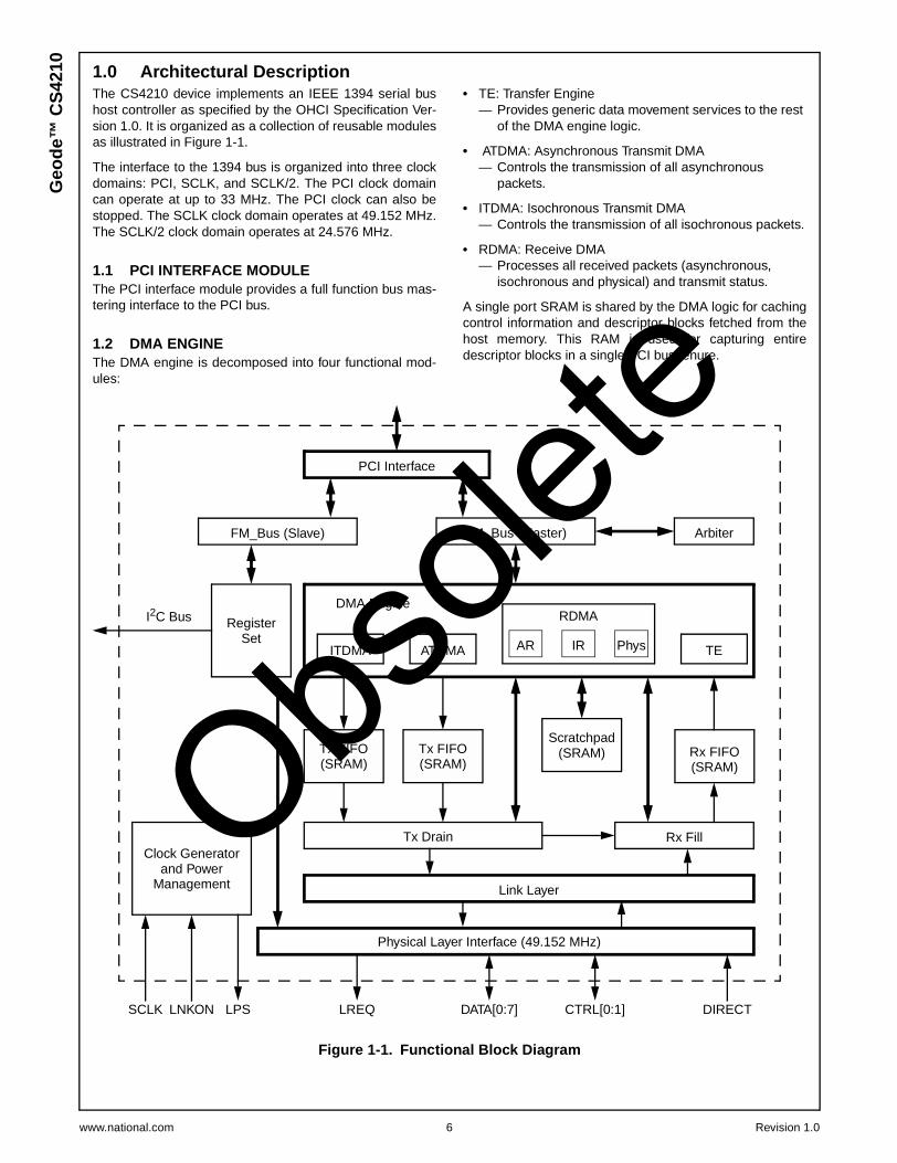
4210 1.0 Architectural Description
The CS4210 device implements an IEEE 1394 serial bushost controller as specified by the OHCI Specification Ver-sion 1.0. It is organized as a collection of reusable modulesas illustrated in Figure 1-1.
The interface to the 1394 bus is organized into three clockdomains: PCI, SCLK, and SCLK/2. The PCI clock domaincan operate at up to 33 MHz. The PCI clock can also bestopped. The SCLK clock domain operates at 49.152 MHz.The SCLK/2 clock domain operates at 24.576 MHz.
1.1 PCI INTERFACE MODULEThe PCI interface module provides a full function bus mas-tering interface to the PCI bus.
1.2 DMA ENGINEThe DMA engine is decomposed into four functional mod-ules:
• TE: Transfer Engine— Provides generic data movement services to the rest
of the DMA engine logic.
• ATDMA: Asynchronous Transmit DMA— Controls the transmission of all asynchronous
packets.
• ITDMA: Isochronous Transmit DMA— Controls the transmission of all isochronous packets.
• RDMA: Receive DMA— Processes all received packets (asynchronous,
isochronous and physical) and transmit status.
A single port SRAM is shared by the DMA logic for cachingcontrol information and descriptor blocks fetched from thehost memory. This RAM is used for capturing entiredescriptor blocks in a single PCI bus tenure.
Figure 1-1. Functional Block Diagram
ITDMA
RDMA
ArbiterFM_Bus (Master)FM_Bus (Slave)
PCI Interface
RegisterSet
Clock Generatorand Power
Management
Tx FIFO(SRAM)
Scratchpad(SRAM) Rx FIFO
(SRAM)
Tx Drain Rx Fill
Link Layer
Physical Layer Interface (49.152 MHz)
SCLK LREQ DATA[0:7] CTRL[0:1] DIRECT
DMA Engine
PhysATDMA TEIRAR
Tx FIFO(SRAM)
I2C Bus
LNKON LPS
Obsole
te

Revision 1.0 7 www.national.com
Geo
de™
CS
4210Architectural Description (Continued)
1.2.1 Transfer EngineThe transfer engine performs data movement between dif-ferent sources/sinks:
1) Host memory (TxFIFOs/RxFIFO, Scratchpad SRAM)
2) DMA modules (ATDMA, ITDMA, or RDMA)
All byte alignment and byte swapping tasks are also per-formed by the transfer engine.
1.2.2 Host Memory OrganizationThe 1394 OHCI specification allows for many different dataFIFO implementations. This CS4210 implements two trans-mit FIFOs (asynchronous and isochronous) and a singlereceive FIFO. The transmit FIFOs share a single embed-ded dual-port SRAM (36x1024). The receive FIFO uses asingle embedded dual-port SRAM (36x1024). A smalltransmit FIFO is also implemented using latches and somedecoding logic.
All FIFOs may be tested using an embedded RAM BISTcontroller. See Section 4.5.4 "nscRAMBist" on page 94 formore details.
1.2.3 ATDMAThe ATDMA module controls the transmission of all asyn-chronous packets. This includes AT (Asynchronous Trans-mit) Request context packets, AT Response contextpackets and all physical DMA transmit request andresponse packets. The ATDMA module also controlsretransmission of packets as required by the OHCI specifi-cation.
1.2.4 ITDMAThe ITDMA module controls the transmission of all isochro-nous packets. Annex E of the OHCI specification describesthe operation of the ITDMA module. This annex was con-tributed by National Semiconductor.
1.2.5 RDMAThe RDMA module processes all received packets andtransmit status. This includes packets destined for the AR(Asynchronous Receive) Request context, AR Responsecontext, all IR (Isochronous Receive) contexts, the Self-IDbuffer, and all physical DMA requests (including CSRaccesses). It also examines the transmit status to managethe collection of currently active physical DMA requests.
1.3 TRANSMIT DRAINThe transmit drain module accepts packets from theTxFIFOs (asynchronous and isochronous) and interfaceswith the link layer module to transmit these packets. It alsoplaces transmit completion status in the TxFIFO.
1.4 RECEIVE FILLThe receive fill module accepts packets from the link layerand places them into the RxFIFO. It performs packet filter-ing and routing. It also determines which handshake, if any,to return for each received packet.
1.5 LINK LAYERThe link layer module implements a 1394 link layer functiondeveloped for this host controller application. It includessupport for the CRC32 generation/checking, link statemachine, transmit/receive data paths and the generation/reception of cycle start packets. This module includes sup-port for features defined in the P1394a supplement.
1.6 PHYSICAL LAYER INTERFACEThe physical layer interface module implements the exter-nal interface to connect to the Geode CS4103 P1394aphysical layer device. It includes support for featuresdefined in revision 2.0 of the P1394a specification.
1.7 REGISTER SETThe register set module coordinates slave accesses to thehost controller registers. It fields read/write requests fromthe PCI interface module. It can also read configurationdata from a serial EEPROM device via an I2C interface.
1.8 RELATED DOCUMENTSThe following documents may be useful in understandingthe terms and concepts used in this publication.
• 1394 Open Host Controller Interface SpecificationRelease 1.0
• IEEE 1394-1995 High Performance Serial Bus, 1995
• ISO/IEC 13213:1994 Control and Status Register Archi-tecture for Microcomputer Buses International Stan-dards Organization, 1994
• IEEE P1394a Standard for a High Performance Serialbus (Supplement)
Obsole
te

www.national.com 8 Revision 1.0
Geo
de™
CS
4210 2.0 Signal Definitions
This section defines the signals and external interface ofthe CS4210. Figure 2-1 shows the pins organized by theirfunctional groupings (internal test and electrical pins arenot shown).
2.1 PIN ASSIGNMENTThe tables in this section use several common abbrevia-tions. Table 2-1 lists the mnemonics and their meanings.
Figure 2-2 on page 9 shows the pin assignment for theCS4210 with Tables 2-2 and 2-3, on pages 10 and 11, list-ing the pin assignments sorted by pin number and alpha-betically by signal name.
Section 2.2 "Signal Descriptions" starting on page 12 pro-vides a description for each signal within its associatedfunctional group.
Figure 2-1. Signal Groups
Table 2-1. Pin Type Definitions
Mnemonic Definition
I Input Pin
I/O Bidirectional Pin
O Output
t/s TRI-STATE Signal
VDD 2.5V Core Power Supply
VDDIO 3.3V I/O Power Supply
VSS Ground Connection
AD[31:0]C/BE[3:0]#
FRAME#IRDY#
TRDY#STOP#
DEVSEL#IDSEL
DATA[0:7]CTRL[0:1]LREQSCLKLPSLNKONDIRECT
PHY-LinkInterface
PCI BusInterface
Geode™PERR#SERR#
PARPREQ#PGNT#
INTA#RST#PCLKPME#
EECLKEEDATA
CCLKOCCLKI
CMCCMCL
I2CCS4210Interface
8 kHz Reference
Contender
Clock Interface
Master ControlInterface
Obsole
te

Revision 1.0 9 www.national.com
Geo
de™
CS
4210Signal Definitions (Continued)
Figure 2-2. Pin Assignment DiagramOrder Number: CS4210VJG
Geode™ CS4210
12345
678910111213
1415161718
19202122
232425
26 27 28 29 30 31 32 33 34 35 36 37 38 39 40 41 42 43 44 45 46 47 48 49 50
Top View
VSSCMC
CMCLEECLK
EEDATAVDDIOTESTO
INTA#VDD
RST#VSS
PCLKVDD
PGNT#PREQ#VDDIOPME#AD31
AD30VDD
AD29AD28
AD27VSS
AD26
7574737271
70696867666564636261605958
57565554
535251
100 99 98 97 96 95 94 93 92 91 90 89 88 87 86 85 84 83 82 81 80 79 78 77 76
AD
25A
D24
C/B
E3#
IDS
EL
VS
S
AD
23A
D22
AD
21A
D20
VD
DA
D19
AD
18A
D17
VD
DIO
AD
16C
/BE
2#
FR
AM
E#
IRD
Y#
TR
DY
#V
DD
DE
VS
EL#
STO
P#
PE
RR
#V
SS
VS
S
VSSAD0AD1AD2AD3VDDAD4AD5AD6AD7C/BE0#AD8VDDIOAD9AD10VSSAD11AD12
AD13AD14VDDAD15
C/BE1#PARSERR#
VS
SLP
SLN
KO
NLR
EQ
VD
DS
CLK
VS
SC
TR
L0C
TR
L1V
DD
DAT
A0
DAT
A1
DAT
A2
VD
DIO
DAT
A3
DAT
A4
DAT
A5
VS
SD
ATA
6D
ATA
7V
DD
DIR
EC
TC
CLK
IC
CLK
OT
ES
TE
N#
Obsole
te

www.national.com 10 Revision 1.0
Geo
de™
CS
4210 Signal Definitions (Continued)
Table 2-2. Pin Assignment - Sorted by Pin Number
PinNo. Signal Type
1 VSS GND
2 CMC O
3 CMCL O
4 EECLK O
5 EEDATA I
6 VDDIO PWR
7 TESTO O
8 INTA# O
9 VDD PWR
10 RST# O
11 VSS GND
12 PCLK I
13 VDD PWR
14 PGNT# I
15 PREQ# O
16 VDDIO PWR
17 PME# O
18 AD31 I/O
19 AD30 I/O
20 VDD PWR
21 AD29 I/O
22 AD28 I/O
23 AD27 I/O
24 VSS GND
25 AD26 I/O
26 AD25 I/O
27 AD24 I/O
28 C/BE3# I/O
29 IDSEL I
30 VSS GND
31 AD23 I/O
32 AD22 I/O
33 AD21 I/O
34 AD20 I/O
35 VDD PWR
36 AD19 I/O
37 AD18 I/O
38 AD17 I/O
39 VDDIO PWR
40 AD16 I/O
41 C/BE2# I/O
42 VSS GND
43 FRAME# I/O
44 IRDY# I/O
45 TRDY# I/O
46 VDD PWR
47 DEVSEL# I/O
48 STOP# I/O
49 PERR# I/O
50 VSS GND
51 SERR# I/O
52 PAR I/O
53 C/BE1# I/O
54 AD15 I/O
55 VDD PWR
56 AD14 I/O
57 AD13 I/O
58 AD12 I/O
59 AD11 I/O
60 VSS GND
61 AD10 I/O
62 AD9 I/O
63 VDDIO PWR
64 AD8 I/O
65 C/BE0# I/O
66 AD7 I/O
67 AD6 I/O
68 AD5 I/O
PinNo. Signal Type
69 AD4 I/O
70 VDD PWR
71 AD3 I/O
72 AD2 I/O
73 AD1 I/O
74 AD0 I/O
75 VSS GND
76 TESTEN# I
77 CCLKO O
78 CCLKI I
79 DIRECT I
80 VDD PWR
81 DATA7 I/O
82 DATA6 I/O
83 VSS GND
84 DATA5 I/O
85 DATA4 I/O
86 DATA3 I/O
87 VDDIO PWR
88 DATA2 I/O
89 DATA1 I/O
90 DATA0 I/O
91 VDD PWR
92 CTRL1 I/O
93 CTRL0 I/O
94 VSS GND
95 SCLK I
96 VDD PWR
97 LREQ O
98 LNKON I
99 LPS O
100 VSS GND
PinNo. Signal Type
Obsole
te
Revision 1.0 11 www.national.com
Geo
de™
CS
4210Signal Definitions (Continued)
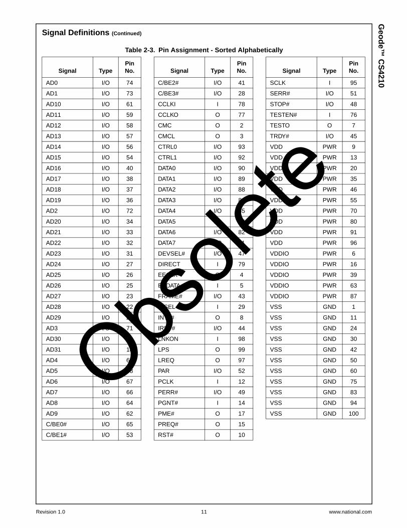
Table 2-3. Pin Assignment - Sorted Alphabetically
Signal TypePinNo.
AD0 I/O 74
AD1 I/O 73
AD10 I/O 61
AD11 I/O 59
AD12 I/O 58
AD13 I/O 57
AD14 I/O 56
AD15 I/O 54
AD16 I/O 40
AD17 I/O 38
AD18 I/O 37
AD19 I/O 36
AD2 I/O 72
AD20 I/O 34
AD21 I/O 33
AD22 I/O 32
AD23 I/O 31
AD24 I/O 27
AD25 I/O 26
AD26 I/O 25
AD27 I/O 23
AD28 I/O 22
AD29 I/O 21
AD3 I/O 71
AD30 I/O 19
AD31 I/O 18
AD4 I/O 69
AD5 I/O 68
AD6 I/O 67
AD7 I/O 66
AD8 I/O 64
AD9 I/O 62
C/BE0# I/O 65
C/BE1# I/O 53
C/BE2# I/O 41
C/BE3# I/O 28
CCLKI I 78
CCLKO O 77
CMC O 2
CMCL O 3
CTRL0 I/O 93
CTRL1 I/O 92
DATA0 I/O 90
DATA1 I/O 89
DATA2 I/O 88
DATA3 I/O 86
DATA4 I/O 85
DATA5 I/O 84
DATA6 I/O 82
DATA7 I/O 81
DEVSEL# I/O 47
DIRECT I 79
EECLK O 4
EEDATA I 5
FRAME# I/O 43
IDSEL I 29
INTA# O 8
IRDY# I/O 44
LNKON I 98
LPS O 99
LREQ O 97
PAR I/O 52
PCLK I 12
PERR# I/O 49
PGNT# I 14
PME# O 17
PREQ# O 15
RST# O 10
Signal TypePinNo.
SCLK I 95
SERR# I/O 51
STOP# I/O 48
TESTEN# I 76
TESTO O 7
TRDY# I/O 45
VDD PWR 9
VDD PWR 13
VDD PWR 20
VDD PWR 35
VDD PWR 46
VDD PWR 55
VDD PWR 70
VDD PWR 80
VDD PWR 91
VDD PWR 96
VDDIO PWR 6
VDDIO PWR 16
VDDIO PWR 39
VDDIO PWR 63
VDDIO PWR 87
VSS GND 1
VSS GND 11
VSS GND 24
VSS GND 30
VSS GND 42
VSS GND 50
VSS GND 60
VSS GND 75
VSS GND 83
VSS GND 94
VSS GND 100
Signal TypePinNo.
Obsole
te

www.national.com 12 Revision 1.0
Geo
de™
CS
4210 Signal Definitions (Continued)
2.2 SIGNAL DESCRIPTIONS
2.2.1 PCI Bus Interface Signals
Signal Name Pin No. Type Description
AD[31:0] Refer toTable 2-3
I/O Multiplexed Address and Data
AD[31:0] is a physical address during the first clock of a PCI transaction; it isthe data during subsequent clocks.
When the CS4210 is a PCI master, AD[31:0] are outputs during the addressand write data phases, and are inputs during the read data phase of a trans-action.
When the CS4210 is a PCI slave, AD[31:0] are inputs during the addressand write data phases, and are outputs during the read data phase of atransaction.
C/BE[3:0]# 65, 53, 41,28
I/O Bus Command and Byte Enables
Multiplexed bus command and byte enables.
FRAME# 43 I/O Cycle Frame
Driven by the initiator to indicate the beginning and duration of an access.
IRDY# 44 I/O Initiator Ready
Indicates that the initiator is ready to complete the current data phase of thetransaction.
TRDY# 45 I/O Target Ready
Indicates that the current data phase of the transaction is ready to be com-pleted.
STOP# 48 I/O Stop
Indicates that the current target is requesting the initiator to stop the currenttransaction.
DEVSEL# 47 I/O Device Select
When actively driven, DEVSEL# indicates the driving device has decodedits address as the target of the current access.
IDSEL 29 I Initialization Device Select
Used as a chip select during configuration read and write transactions.
PERR# 49 I/O Parity Error
Used for reporting data parity errors during all PCI transactions except aSpecial Cycle.
SERR# 51 I/O System Error
Used for reporting address parity errors, data parity errors on the SpecialCycle command, or any other system error where the result will be cata-strophic.
PAR 52 I/O Parity
PAR is even parity across AD[31:0] and C/BE[3:0]. PAR is an input whenAD[31:0] are inputs and is an output when AD[31:0] are outputs.
PREQ# 15 O PCI Bus Request
PCI bus request to PCI bus arbiter.
PGNT# 14 I PCI Bus Grant
PCI bus grant from PCI bus arbiter.
INTA# 8 O Interrupt A
1394 OpenHCI PCI interrupt.
Obsole
te

Revision 1.0 13 www.national.com
Geo
de™
CS
4210Signal Definitions (Continued)
RST# 10 I PCI Reset
RST# is driven low to reset the device.
PCLK 12 I Clock
0-33 MHz PCI clock.
PME# 17 O Power Management Event
PCI power management pin as defined in the PCI Bus Power ManagementSpecification Revision 1.1.
2.2.2 PHY-Link Interface Signals
Signal Name Pin No. I/O Description
DATA[0:7] 81, 82, 84,85, 86, 88,
89, 90
I/O PHY Data
Bidirectional data lines driven by both the Link and PHY layer modules. Thewidth of the data bus depends on the speed of data transfer rate. Packet ratefor 100 Mbit/sec transfers use DATA[0:1], 200 Mbit/sec transfers useDATA[0:3], 400 Mbit/sec transfers use DATA[0:7].
Note: DATA0 is considered the MSB (most significant bit) based upon theIEEE 1394-1995 specification.
CTRL[0:1] 93, 92 I/O Control bits 1 and 0
Bidirectional handshaking signals driven by both the Link and PHY layermodules. The CS4210 and CS4103 use these signals to arbitrate the controlof the PHY-Link interface. The control bits also indicate the type of transfercommunicating between the two layers namely idle, status, receive, andtransmit.
LREQ 97 O Link Request
Used by the CS4210 to request access of the 1394 bus and to read/write theinternal registers of the CS4103.
SCLK 95 I Sync Clock
The 49.152 MHz clock input driven by the CS4103’s PLL block synchronizedto the 1394 bus clock. This clock is also used to synchronize the LREQ,CTRL[0:1], and DATA[0:7] communication protocol between the CS4210and CS4103.
LPS 99 O Link Power Status
Indicates the power status of the CS4210. If LPS is low indicating theCS4210 is not powered, the signals CTRL[0:1], DATA[0:7], and SCLK con-nected to the CS4210 are disabled.
LNKON 98 I Link On
Indicates to the CS4210 that the CS4103 has received a Link-On packetaddressed to this node.
DIRECT 79 I Direct
High indicates direct connection. Low indicates isolation barrier. Set highwhen using the single capacitor bus hold isolation.
2.2.1 PCI Bus Interface Signals (Continued)
Signal Name Pin No. Type Description
Obsole
te

www.national.com 14 Revision 1.0
Geo
de™
CS
4210 Signal Definitions (Continued)
2.2.3 Miscellaneous Interface Signals
Signal Name Pin No. Type Description
EECLK 4 O Serial EEPROM Clock
The I2C bus clock signal.
EEDATA 5 I Serial EEPROM Data
The I2C data signal.
CCLKO 77 O Cycle Clock Output
The 8 kHz reference clock output.
CCLKI 78 I Cycle Clock Input
The 8 kHz reference clock input.
CMC 2 O Contender Master Control
This output is set via the nscCMCControl.CMC bit (BAR1+Offset 18h[0]).The value placed on the bit is directly reflected on this pin.
CMCL 3 O Contender Master Control Link Enabled
This output is set via the nscCMCControl.CMCL bit (BAR1+Offset 18h[1]).The value of the bit is reflected on the output when HCControl.linkEnable(BAR0+Offset 50h[17]) is set. Otherwise it is 0.
TESTO 7 O Test Out
National internal test pin, user must float.
TESTEN# 76 I Test Enable
National internal test pin, user must tie high.
2.2.4 Power Supplies and Ground Connections
Signal Name Pin No. Type Description
VDD 9, 13, 20, 35, 46, 55,70, 80, 91, 96
PWR 2.5V Core Power Supply Connections (Total of 10)
VDDIO 6, 16, 39, 63, 87 PWR 3.3V I/O Power Supply Connections (Total of 5)
VSS 1, 11, 24, 30, 42, 50,60, 75, 83, 94, 100
GND Ground Connections (Total of 11)Obsole
te
Revision 1.0 15 www.national.com
Geo
de™
CS
42103.0 Operational Description
3.1 OVERVIEWThe CS4210 is an implementation of the link layer protocolof the 1394 serial bus, with additional features to supportthe transaction and bus management layers. The CS4210also includes DMA engines for high-performance datatransfer and a PCI host bus interface. IEEE 1394 serial bus(and 1394 OpenHCI) protocols support two types of datatransfer: asynchronous and isochronous.
• Asynchronous data transfer puts the emphasis on guar-anteed delivery of data, with less emphasis on guaran-teed timing.
• Isochronous data transfer is the opposite, with theemphasis on the guaranteed timing of the data, and lessemphasis on delivery.
3.1.1 Asynchronous Data Transfer FunctionsThe CS4210 can transmit and receive all of the defined1394 packet formats. Packets to be transmitted are readout of host memory and received packets are written intohost memory, both using DMA. The CS4210 can also beprogrammed to act as a bus bridge between the host busand 1394 devices by directly executing 1394 read and writerequests as reads and writes to the host bus memoryspace.
3.1.2 Isochronous Data Transfer FunctionsThe CS4210 is capable of performing the cycle masterfunction as defined by the IEEE 1394 OHCI specification.This means it contains a cycle timer and counter, and canqueue the transmission of a special packet called a “cyclestart” after every rising edge of the 8 kHz cycle clock. TheCS4210 can generate the cycle clock internally or use anexternal reference connected to the CCLKI input (pin 78).When not the cycle master, the CS4210 keeps its internalcycle timer synchronized with the cycle master node bycorrecting its own cycle timer with the reload value from thecycle start packet. Conceptually, the CS4210 supports oneDMA controller each for isochronous transmit and isochro-
nous receive. The CS4210 provides eight isochronoustransmit contexts. The isochronous transmit DMA controllercan transmit from each context during each cycle. Eachcontext can transmit data for a single isochronous channel.The CS4210 provides eight isochronous receive contexts.The isochronous receive DMA controller can receive datafor each context during each cycle. Each context can beconfigured to receive data from a single isochronous chan-nel. Additionally, one context can be configured to receivedata from multiple isochronous channels (see bit 28, multi-ChanMode, in Table 4-53 on page 87 for programmingdetails).
3.1.3 Miscellaneous FunctionsUpon detecting a bus reset, the CS4210 automaticallyflushes all packets queued for asynchronous transmission.Asynchronous packet reception continues without interrup-tion, and a token appears in the received request packetstream to indicate the occurrence of the bus reset. Whenthe CS4103 provides the new local node ID, the CS4210loads this value into its Node ID register, see Table 3-1.Asynchronous packet transmit will not resume untildirected to by software. Because target node ID valuesmay have changed during the bus reset, software will notgenerally be able to re-issue old asynchronous requestsuntil software has determined the new target node IDs. Iso-chronous transmit and receive functions are not halted by abus reset, instead they restart as soon as the bus initializa-tion process is complete. A number of management func-tions are also implemented by the CS4210. A global uniqueID register, shown in Table 3-2, can only be written once.For full compliance with higher level standards, this registermust be written before the boot block is read. To make thisimplementation simpler, the CS4210 has an interface to anexternal serial I2C EEPROM such as the Fairchild Semi-conductor NM24C02. The CS4210 also supports four reg-isters that implement the compare-swap operation neededfor isochronous resource management.
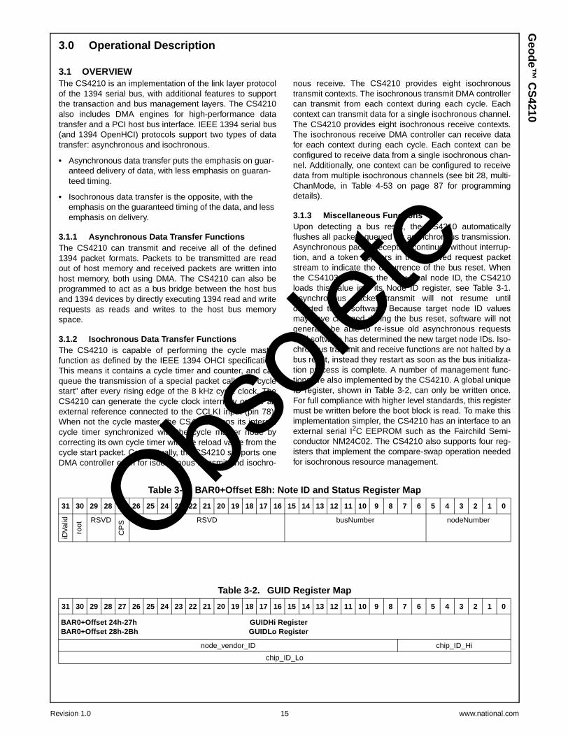
Table 3-1. BAR0+Offset E8h: Note ID and Status Register Map
31 30 29 28 27 26 25 24 23 22 21 20 19 18 17 16 15 14 13 12 11 10 9 8 7 6 5 4 3 2 1 0
iDV
alid
root
RSVD
CP
S RSVD busNumber nodeNumber
Table 3-2. GUID Register Map
31 30 29 28 27 26 25 24 23 22 21 20 19 18 17 16 15 14 13 12 11 10 9 8 7 6 5 4 3 2 1 0
BAR0+Offset 24h-27h GUIDHi RegisterBAR0+Offset 28h-2Bh GUIDLo Register
node_vendor_ID chip_ID_Hi
chip_ID_Lo
Obsole
te

www.national.com 16 Revision 1.0
Geo
de™
CS
4210 Operational Description (Continued)
3.2 SOFTWARE INTERFACE OVERVIEWThere are three basic means by which software communi-cates with the CS4210: registers, DMA, and interrupts.
3.2.1 RegistersThe host architecture (PCI, for example) is responsible formapping the CS4210’s registers into a portion of the host’saddress space.
3.2.2 DMA OperationDMA transfers in the CS4210 are accomplished throughone of two methods: DMA memory and physical responseDMA.
3.2.2.1 DMA MemoryDMA memory resident data structures are used to describelists of data buffers. The CS4210 automatically sequencesthrough this buffer descriptor list. This data structure alsocontains status information regarding the transfers. Uponcompletion of each data transfer, the DMA controller condi-tionally updates the corresponding DMA context commandand conditionally interrupts the processor so it can observethe status of the transaction. A set of registers within theCS4210 is used to initialize each DMA context and to per-form control actions such as starting the transfer.
3.2.2.2 Physical Response DMAThe CS4210 can be programmed to accept 1394 read andwrite transactions as reads and writes to host memoryspace. In this mode, the CS4210 acts as a bus bridge fromthe 1394 bus into host memory. The formats for the datasent and received in all these modes are specified in the1394 Open Host Controller Interface Specification Release1.00.
3.2.3 InterruptsWhen any DMA transfer completes (or aborts), an interruptmay be sent to the host system. In addition to the interrupt
sources which correspond to each DMA context comple-tion, there is also a set of interrupts which correspond toother CS4210 functions/units. For example, one of theseinterrupts could be sent when a Self-ID packet stream hasbeen received. The processor interrupt line is controlled bythe IntEvent and IntMask registers. The IntEvent registerindicates which interrupt events have occurred, and the Int-Mask register is used to enable selected interrupts. Soft-ware writes to the IntEventClear register to clear interruptconditions in IntEvent. In addition, there are registers usedby the isochronous transmit and isochronous receive con-trollers to indicate interrupt conditions for each context.
Table 3-3 shows a map of the IntEvent and IntMask Set/Clear registers. Refer to Section 4.4.16.1 "IntEvent Regis-ter" on page 70 and Section 4.4.16.3 "IntMask Register" onpage 72 for further information details.
3.2.3.1 Asynchronous Transmit InterruptsEach asynchronous DMA context has one interrupt indica-tion bit in the IntEvent register. For requests, it is the reqTx-Complete bit and for responses it is the respTxCompletebit. This interrupt indication bit is set to one if a completedOUTPUT_LAST command has the “i” field set to 11b, or ifthe “i” field is set to 01b and transmission of the packet didnot yield an ack_complete or an ack_pending.
3.2.3.2 Asynchronous Receive InterruptsThere are two interrupts for each context (request andresponse) that software can use to gauge the usage of thereceive buffers. If software needs to be informed of thearrival of each packet being sent to the context buffers, itcan use the RQPkt or RSPkt interrupts in the IntEvent reg-ister. If software needs to be informed of the completion ofa buffer, it can set the descriptor i field to 11b, which trig-gers either the ARRQ or ARRS interrupt in the IntEventregister.
Table 3-3. IntEvent and IntMask Register Map
31 30 29 28 27 26 25 24 23 22 21 20 19 18 17 16 15 14 13 12 11 10 9 8 7 6 5 4 3 2 1 0
BAR0+Offset 80h IntEvent Set RegisterBAR0+Offset 84h IntEvent Clear Register
RSVD
phyR
egR
cvd
cycl
eToo
Long
unre
cove
rabl
eErr
or
cycl
eInc
onsi
sten
t
cycl
eLos
t
cycl
e64S
econ
ds
cycl
eSyn
ch
phy
RS
VD
busR
eset
selfI
Dco
mpl
ete
RSVD
lock
Res
pErr
post
edW
riteE
rr
isoc
hRx
isoc
hTx
RS
Pkt
RQ
Pkt
AR
RS
AR
RQ
resp
TxC
ompl
ete
reqT
xCom
plet
e
BAR0+Offset 88h IntMask Set RegisterBAR0+Offset 8Ch IntMask Clear Register
mas
terI
ntE
nabl
e RSVD
phyR
egR
cvd
cycl
eToo
Long
unre
cove
rabl
eErr
or
cycl
eInc
onsi
sten
t
cycl
eLos
t
cycl
e64S
econ
ds
cycl
eSyn
ch
phy
RS
VD
busR
eset
selfI
Dco
mpl
ete
RSVD
lock
Res
pErr
post
edW
riteE
rr
isoc
hRx
isoc
hTx
RS
Pkt
RQ
Pkt
AR
RS
AR
RQ
resp
TxC
ompl
ete
reqT
xCom
plet
e
Obsole
te

Revision 1.0 17 www.national.com
Geo
de™
CS
4210Operational Description (Continued)
3.2.3.3 Isoch Tx and Rx Context InterruptsEach of the eight implemented isochronous transmit andeach of the eight implemented isochronous receive con-texts can generate an interrupt. Software can enable inter-rupts on a per-context basis by setting the correspondingIsochTxnContextIntMask or IsochRxnContextIntMask bit toone. To efficiently handle interrupts which could conceiv-ably be generated from eight different contexts in closeproximity to one another, there is a single bit for all IT DMAcontexts and another for all IR DMA contexts in theCS4210 IntEvent register. These bits signify that at leastone but potentially several IT or IR DMA contextsattempted to generate an interrupt. Software can read theisochTxIntEvent register to find out which isochronoustransmit context(s) are involved. Software can read the Iso-
chRxIntEvent register to find out which isochronous receivecontext(s) are involved.
Table 3-4 shows a map of the IsochTx/Rx Context InterruptEvent and Mask Set/Clear registers. Refer to Section4.4.16.4 on page 73 through Section 4.4.16.7 on page 74for further register information.
The number of supported isochronous DMA contexts var-ies for 1394 OHCI implementations from a minimum of fourto a maximum of 32. Software can determine the numberof supported IT or IR DMA contexts by writingFFFF_FFFFh to IsochTxIntMask register for IT and Isoch-RxIntMask register for IR, and then reading it back. Bitsreturned as 1’s indicate supported contexts, and bitsreturned as 0’s indicate unsupported/unimplemented con-texts.
Table 3-4. IsochTx and IsochRx Context Interrupt Related Registers
31 30 29 28 27 26 25 24 23 22 21 20 19 18 17 16 15 14 13 12 11 10 9 8 7 6 5 4 3 2 1 0
BAR0+Offset 90h IsochTxIntEvent Set RegisterBAR0+Offset 94h IsochTxIntEvent Clear Register
RSVD
isoc
hTxI
nt7
isoc
hTxI
nt6
isoc
hTxI
nt5
isoc
hTxI
nt4
isoc
hTxI
nt3
isoc
hTxI
nt2
isoc
hTxI
nt1
isoc
hTxI
nt0
BAR0+Offset 98h IsochTxIntMask Set RegisterBAR0+Offset 9Ch IsochTxIntMask Clear Register
RSVD
isoc
hTxI
ntM
ask7
isoc
hTxI
ntM
ask6
isoc
hTxI
ntM
ask5
isoc
hTxI
ntM
ask4
isoc
hTxI
ntM
ask3
isoc
hTxI
ntM
ask2
isoc
hTxI
ntM
ask1
isoc
hTxI
ntM
ask0
BAR0+Offset A0h IsochRxIntEvent Set RegisterBAR0+Offset A4h IsochRxIntEvent Clear Register
RSVD
isoc
hRxI
nt7
isoc
hRxI
nt6
isoc
hRxI
nt5
isoc
hRxI
nt4
isoc
hRxI
nt3
isoc
hRxI
nt2
isoc
hRxI
nt1
isoc
hRxI
nt0
BAR0+Offset A8h IsochRxIntMaskSet RegisterBAR0+Offset ACh IsochRxIntMaskClear Register
RSVD
isoc
hRxI
ntM
ask7
isoc
hRxI
ntM
ask6
isoc
hRxI
ntM
ask5
isoc
hRxI
ntM
ask4
isoc
hRxI
ntM
ask3
isoc
hRxI
ntM
ask2
isoc
hRxI
ntM
ask1
isoc
hRxI
ntM
ask0Obs
olete

www.national.com 18 Revision 1.0
Geo
de™
CS
4210 Operational Description (Continued)
When the IntEvent.cycleInconsistent condition occurs, theIT and IR DMA controllers continue processing runningcontexts normally, except that contexts with the Context-Control.cycleMatchEnable bit set remain inactive andcycleMatch processing is, in effect, disabled. To re-enablecycleMatch processing, software must first stop the IT and/or IR contexts for which cycleMatch is enabled (by clearingContextControl.run and waiting for ContextControl.active toclear, then clearing the IntEvent.cycleInconsistent interrupt(read BAR0+Offset 84h[23]). The stopped IR contexts may
then be started. The stopped IT contexts may also bestarted, but software should not schedule any transmits tooccur for these contexts for at least two cycles immediatelyfollowing the clearing of the interrupt condition.
Table 3-5 is a register format for the eight IsochronousTransmit Context Control Set/Clear registers. Refer to Sec-tion 4.4.26.1 "Isoch Transmit Context Control Register" onpage 84 for further register information.
Table 3-5. IsochTx[7:0]ContextControl Set/Clear Register Formats
31 30 29 28 27 26 25 24 23 22 21 20 19 18 17 16 15 14 13 12 11 10 9 8 7 6 5 4 3 2 1 0
IsochTxnContextControl Set RegisterIsochTxnContextControl Clear Register
cycl
eMat
chE
nabl
e cycleMatch
run
RSVD
wak
e
dead
activ
e
RSVD event code
Obsole
te

Revision 1.0 19 www.national.com
Geo
de™
CS
4210Operational Description (Continued)
3.3 COMMON DMA CONTROLLER FEATURESThe CS4210 provides several types of DMA functionality:
• General-purpose DMA handling asynchronous transmitand receive packets and isochronous transmit andreceive packets.
• An inbound bus bridge function that allows 1394 devicesto directly access system memory called “physicalDMA.”
• A separate write buffer for the received Self-ID packets.
• A mapping between a 1 KB block in system memory andthe first 1K of configuration ROM.
3.3.1 Context RegistersA context provides the basic information to the CS4210 toallow it to fetch and process descriptors for one of the sev-eral DMA controllers. All contexts (except for Self-ID) havea ContextControl register and a CommandPtr register. Theformat of the ContextControl Registers is DMA controllerspecific.
Table 3-6 is a register format of the Contex.Control andCommandPtr registers. Refer to Section 4.4.24 starting on
page 80 through Section 4.4.27 for further register informa-tion.
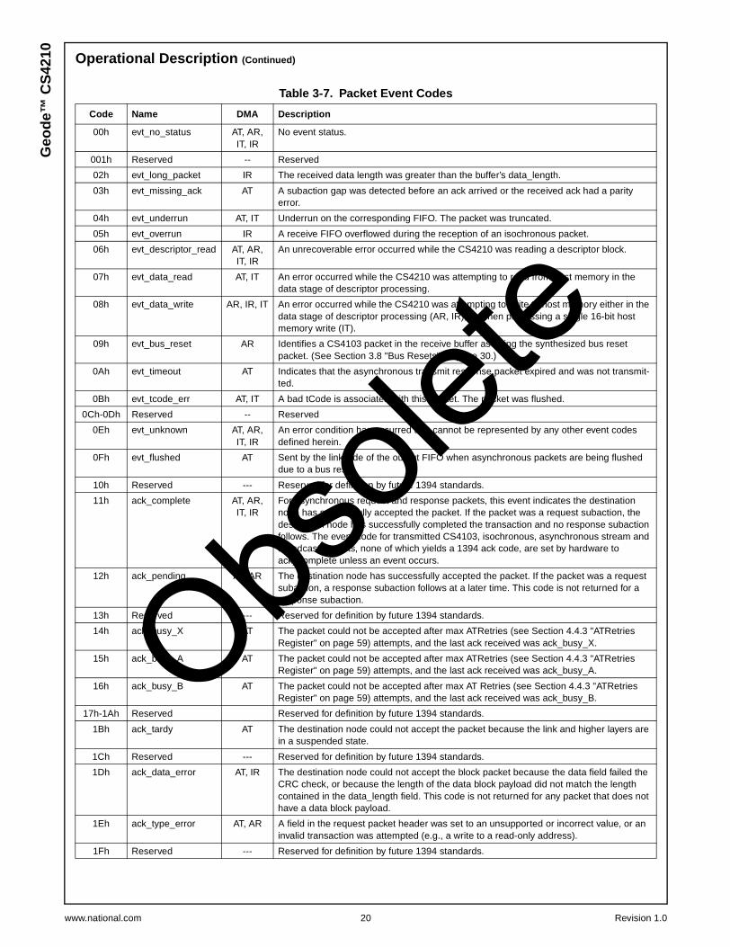
3.3.2 ContextControl.eventThe packet event codes shown in Table 3-7 on page 20 arepossible values for the five-bit ContextControl.event field.This field may contain either a 1394 defined ack code or anOpenHCI generated event code. Bits [15:0] of the Context-Control register may be written into host memory to indi-cate packet and/or DMA descriptor status. However, allpossible event codes which may appear in a particular con-text’s ContextControl register may not necessarily ever bewritten into host memory for a packet or DMA descriptorstatus, depending on circumstances and the functionality ofthe context. The list of ack codes provided in Table 3-7 isinformative not normative (i.e., for asynchronous packetsthe event code may be set to any ack code specified in cur-rent and future 1394 standards). OpenHCI generated eventcodes have an “evt_” prefix and are denoted by a code withthe high (fifth) bit equal to 0. In some cases for isochronousI/O OpenHCI may generate a 1394 style ack code for Con-textControl.event.
Table 3-6. ContextControl and CommandPtr Registers Formats
31 30 29 28 27 26 25 24 23 22 21 20 19 18 17 16 15 14 13 12 11 10 9 8 7 6 5 4 3 2 1 0
AsyncReqTxContextControl Set/Clear RegistersAsyncRespTxContextControl Set/Clear Registers
RSVD
run RSVD
wak
e
dead
activ
e RSVD event code
AsyncReqRxContextControl Set/Clear RegistersAsyncRespRxContextControl Set/Clear Registers
RSVD
run RSVD
wak
e
dead
activ
e RSVD spd event code
IsochTxnContextControl Set/Clear Registers
cycl
eMat
chE
nabl
e cycleMatch
run
RSVD
wak
e
dead
activ
e
RSVD event code
IsochRxnContextControl Set/Clear Registers
buffe
rFill
isoc
hhea
der
Cyc
leM
atch
Ena
ble
mul
tiCha
nMod
e RSVD
run
RSVD
wak
e
dead
activ
e
RSVD spd event code
CommandPtr Register
descriptorAddress Z
Obsole
te
www.national.com 20 Revision 1.0
Geo
de™
CS
4210 Operational Description (Continued)
Table 3-7. Packet Event Codes
Code Name DMA Description
00h evt_no_status AT, AR,IT, IR
No event status.
001h Reserved -- Reserved
02h evt_long_packet IR The received data length was greater than the buffer’s data_length.
03h evt_missing_ack AT A subaction gap was detected before an ack arrived or the received ack had a parityerror.
04h evt_underrun AT, IT Underrun on the corresponding FIFO. The packet was truncated.
05h evt_overrun IR A receive FIFO overflowed during the reception of an isochronous packet.
06h evt_descriptor_read AT, AR,IT, IR
An unrecoverable error occurred while the CS4210 was reading a descriptor block.
07h evt_data_read AT, IT An error occurred while the CS4210 was attempting to read from host memory in thedata stage of descriptor processing.
08h evt_data_write AR, IR, IT An error occurred while the CS4210 was attempting to write to host memory either in thedata stage of descriptor processing (AR, IR), or when processing a single 16-bit hostmemory write (IT).
09h evt_bus_reset AR Identifies a CS4103 packet in the receive buffer as being the synthesized bus resetpacket. (See Section 3.8 "Bus Resets" on page 30.)
0Ah evt_timeout AT Indicates that the asynchronous transmit response packet expired and was not transmit-ted.
0Bh evt_tcode_err AT, IT A bad tCode is associated with this packet. The packet was flushed.
0Ch-0Dh Reserved -- Reserved
0Eh evt_unknown AT, AR,IT, IR
An error condition has occurred that cannot be represented by any other event codesdefined herein.
0Fh evt_flushed AT Sent by the link side of the output FIFO when asynchronous packets are being flusheddue to a bus reset.
10h Reserved --- Reserved for definition by future 1394 standards.
11h ack_complete AT, AR,IT, IR
For asynchronous request and response packets, this event indicates the destinationnode has successfully accepted the packet. If the packet was a request subaction, thedestination node has successfully completed the transaction and no response subactionfollows. The event code for transmitted CS4103, isochronous, asynchronous stream andbroadcast packets, none of which yields a 1394 ack code, are set by hardware toack_complete unless an event occurs.
12h ack_pending AT, AR The destination node has successfully accepted the packet. If the packet was a requestsubaction, a response subaction follows at a later time. This code is not returned for aresponse subaction.
13h Reserved --- Reserved for definition by future 1394 standards.
14h ack_busy_X AT The packet could not be accepted after max ATRetries (see Section 4.4.3 "ATRetriesRegister" on page 59) attempts, and the last ack received was ack_busy_X.
15h ack_busy_A AT The packet could not be accepted after max ATRetries (see Section 4.4.3 "ATRetriesRegister" on page 59) attempts, and the last ack received was ack_busy_A.
16h ack_busy_B AT The packet could not be accepted after max AT Retries (see Section 4.4.3 "ATRetriesRegister" on page 59) attempts, and the last ack received was ack_busy_B.
17h-1Ah Reserved Reserved for definition by future 1394 standards.
1Bh ack_tardy AT The destination node could not accept the packet because the link and higher layers arein a suspended state.
1Ch Reserved --- Reserved for definition by future 1394 standards.
1Dh ack_data_error AT, IR The destination node could not accept the block packet because the data field failed theCRC check, or because the length of the data block payload did not match the lengthcontained in the data_length field. This code is not returned for any packet that does nothave a data block payload.
1Eh ack_type_error AT, AR A field in the request packet header was set to an unsupported or incorrect value, or aninvalid transaction was attempted (e.g., a write to a read-only address).
1Fh Reserved --- Reserved for definition by future 1394 standards.
Obsole
te

Revision 1.0 21 www.national.com
Geo
de™
CS
4210Operational Description (Continued)
3.3.2.1 ContextControl.runThe ContextControl.run bit is set by software when theCS4210 is to begin processing descriptors for the context.Before software sets ContextControl.run, ContextCon-trol.active must not be set, and the CommandPtr registerfor the context must contain a valid descriptor blockaddress and a Z value that is appropriate for the descriptorblock address. Software may stop the CS4210 from furtherprocessing of a context by clearing ContextControl.run.When a ContextControl.run is cleared, the CS4210 willstop processing of the context in a manner that will notimpact the operation of any other context or DMA control-ler. The CS4210 may require a significant amount of timeto safely stop processing for a context but when theCS4210 does stop, it clears ContextControl.active. If soft-ware clears a ContextControl.run for an isochronous con-text while the CS4210 is processing a packet for thecontext, the CS4210 continues to receive or transmit thepacket and update descriptor status. The CS4210 does,however, stop at the conclusion of that packet. If Context-Control.run is cleared for a non-isochronous context, theCS4210 may stop processing at any convenient point aslong as the context and descriptors end up in a consistentstate (e.g., status updated if a packet was sent andacknowledged). Clearing ContextControl.run may haveother side effects that are DMA controller dependent.These effects are described in the subsections of Section4.4 "OHCI Configuration Registers" starting on page 48that cover each of the DMA controllers. When softwareclears ContextControl.run and the CS4210 has stopped,the CS4210 is not necessarily in a state that can berestarted simply by setting ContextControl.run. Softwareshould always ensure that CommandPtr.descriptorAddressand CommandPtr.Z are set to valid values before settingContextControl.run.
3.3.2.2 ContextControl.wakeWhen software adds to a list of descriptors for a context,the CS4210 may have already read the descriptor that wasat the end of the list before it was updated. The value thatthe CS4210 read may contain a Z value of zero indicatingthe end of the descriptor list. The ContextControl.wake bitprovides a simple semaphore to the hardware to indicatethat the list may have changed since the last time theCS4210 read a descriptor. Therefore, if the CS4210 hadfetched a descriptor and the indicated branch address hada Z value of zero, then the CS4210 rereads the pointervalue.
For transmit contexts and receive contexts in buffer-fillmode (a mode in which a context can receive multiplepackets into one data buffer), if the Z value is still zero, thenthe end of the list was reached and the CS4210 clearsContextControl.active. For receive contexts in buffer-fillmode, if the Z value is still zero on the reread, then thepacket cannot be accepted.
For asynchronous contexts, the CS4210 returns the appro-priate ack_busy* code. In addition, the CS4210 “backs out”the packet by not updating the buffer’s byte count (res-Count), and flushes the packet from the FIFO. The CS4210does not go inactive, as there is still buffer space availableand software is attempting to provide more buffer space.For both transmit and receive contexts, if the Z value is nownon-zero, the CS4210 continues processing. In order toensure that a wake condition is not missed, the CS4210clears ContextControl.wake before it reads or rereads adescriptor. ContextControl.wake is ignored when Context-Control.run is zero.
3.3.2.3 ContextControl.activeContextControl.active is set and cleared only by theCS4210. It is set when the CS4210 receives an indicationfrom software that a valid descriptor is available for pro-cessing. This indication occurs as a result of software set-ting the ContextControl.run or by software settingContextControl.wake while ContextControl.run is set.There are four cases in which the CS4210 clears Context-Control.active:
1) When a branch is indicated by a descriptor but the Zvalue of the branch address is 0.
2) When software clears ContextControl.run and theCS4210 has reached a safe stopping point.
3) While ContextControl.dead is set.
4) After a hardware or software reset of the CS4210.
Additionally, for the asynchronous transmit contexts(request and response), the CS4210 clears ContextCon-trol.active when a bus reset occurs. When ContextCon-trol.active is cleared and ContextControl.run is alreadyclear, the CS4210 sets the IntEvent bit for the context. Thisinterrupt is the same interrupt that would have been gener-ated by the context if a completed descriptor had indicatedthat an interrupt should be generated.
3.3.2.4 ContextControl.deadContextControl.dead is used to indicate a fatal error in pro-cessing a descriptor. When ContextControl.dead is set bythe CS4210, ContextControl.active is immediately clearedbut ContextControl.run remains set. In addition, settingContextControl.dead causes an unrecoverableError inter-rupt event and blocks a normal context event interrupt frombeing set. ContextControl.dead is immediately clearedwhen software clears ContextControl.run or by either ahardware or software reset of the CS4210. Software candetermine the cause of a context going dead by checkingthe ContextControl.event code. The defined reasons for theCS4210 to set ContextControl.dead are described in Sec-tion 3.7 "Host Bus Errors" on page 28.
Obsole
te

www.national.com 22 Revision 1.0
Geo
de™
CS
4210 Operational Description (Continued)
3.3.2.5 CommandPtrSoftware initializes CommandPtr.descriptorAddress to con-tain the address of the first descriptor block that theCS4210 accesses when software enables the context bysetting ContextControl.run. Software also initializes Com-mandPtr.Z to indicate the number of descriptors in the firstdescriptor block. Software only writes to this register whenboth ContextControl.run and ContextControl.active arezero. The CS4210’s behavior when this rule is violated isundefined. Since the CS4210 utilizes the CommandPtr reg-ister while processing a context, there is a set of guidelinesby which software may safely and deterministically readCommandPtr. These guidelines are based on the Context-Control bits as listed in Table 3-8 (X = don’t care).
If ContextControl.run is set and ContextControl.dead is notset, then the contents of CommandPtr are only specified ifboth ContextControl.active and ContextControl.wake are
clear. In this instance, CommandPtr.descriptorAddresscontains the address of a descriptor within the last descrip-tor block that was executed. If ContextControl.run and Con-textControl.dead are both set, then descriptorAddresspoints to a descriptor within the descriptor block in whichan unrecoverable error occurred. Except for the casewhere software initializes CommandPtr, the value of Com-mandPtr.Z is undefined and Z may contain a value that isimplementation dependent. The value of CommandPtr isundefined after a hardware or software reset of theCS4210. When software sets ContextControl.run to 1 andCommandPtr.Z contains an invalid value for the controllerand context, or if a Z value is invalid for a fetched descriptorblock in a running context, the CS4210: sets ContextCon-trol.dead to 1 and sets ContextControl.event toevt_unknown and will not process any descriptors in thatcontext.
Table 3-8. CommandPtr Read Values
ContextControl Bits
CommandPtr.descriptor Address Valuerun dead active wake
0 0 0 X A descriptor block address. Either last written or last executed.
0 0 1 X Contents unspecified.
1 0 0 0 Refers to the descriptor block that contains the Z = 0 that caused theCS4210 to set active to 0.
1 0 0 1 Contents unspecified.
1 0 1 0 Contents unspecified.
1 0 1 1 Contents unspecified.
1 1 0 X Points to the descriptor block in which a fatal error occurred.
Obsole
te

Revision 1.0 23 www.national.com
Geo
de™
CS
4210Operational Description (Continued)
3.4 LIST MANAGEMENTAll contexts use an identical method for controlling the pro-cessing of descriptors associated with the context. Thispresents a uniform interface to controlling software andallows reuse of hardware on the CS4210.
3.4.1 Context InitializationSoftware initializes the context by first checking to see thatContextControl.run, ContextControl.active, and Context-Control.dead are all 0. Then, CommandPtr.descriptorAd-dress is written to point to a valid descriptor block andCommandPtr.Z is set to a value that is consistent with thedescriptor block. Then ContextControl.run can be set.
3.4.2 Appending to Running ListSoftware may append to a list of descriptors at any time.Software may append either a single descriptor or a linkedlist of descriptors. When the to-be-appended list is properlyformatted, software updates the branch address and Zvalue of the descriptor that was at the end of the list beingprocessed by the CS4210. When software completes thelinking process it must set ContextControl.wake for the con-text. This ensures that the CS4210 resumes operation if ithad previously reached the end of the list and gone inac-tive.
3.4.3 Stopping a ContextSoftware can stop a running context by clearing Context-Control.run. The context might not stop immediately. Toensure that the context has stopped, software must wait forContextControl.active to be cleared by the CS4210. Thisindicates that the CS4210 has completed all processingassociated with the context.
3.4.4 Hardware BehaviorThe CS4210 has several DMA controllers each of whichhas one or more contexts. Each DMA controller is expectedto examine each of its contexts on a periodic basis andmake operational decisions based on the context state ascontained in ContextControl. The DMA controller examinesthe state of the active, run, wake, and dead bits to governdescriptor processing. This process is executed once eachtime a context is ‘scheduled’. Scheduling of a context isdependent on the DMA controller. For example, an isochro-nous transmit context is scheduled once per cycle while anasynchronous request transmit context is only scheduledonce per fairness interval.
3.5 ASYNCHRONOUS RECEIVEThe CS4210 accepts 1394 transactions and groups themas follows:
Physical Requests - Physical requests, including physicalread, physical write, and lock requests to some CSR regis-ters (see Section 4.4.4 "Autonomous CSR Resources" onpage 60) are handled directly by the CS4210 and are notmade visible to system software. The CS4210 uses a dedi-cated physical response unit to handle these requests. Thisunit will not block processing of other transaction typeswhile dealing with physical requests. Section 3.6 "PhysicalRequests" on page 26 provides details on which requestscan be processed as physical.
Self-ID Packets - CS4103 packets with the Self-ID formatcan be received at any time. However, only those packetsthat are received during the Self-ID phase of bus initializa-tion which immediately follows a bus reset are consideredto be Self-ID packets. Others are considered simply to bePHY packets which are handled like asynchronousrequests. The CS4210 can be programmed to accept orignore Self-ID packets. When Self-ID packets areaccepted, they are stored in a special memory buffer whichhas a dedicated controller and context. Because of thisspecial memory buffer, Self-ID packets can never get‘stuck’ in a FIFO.
Asynchronous Responses - When the host system ini-tiates a request through the asynchronous transmit requestcontext, the response is handled by the asynchronousreceive response context. The fact that host system soft-ware initiates the process and the fact that the CS4210 hasa separate context for responses, allows system softwareto budget for all responses which ensures that the CS4210always has a place in system memory to store a responsewhen it arrives. In the unlikely event that the CS4210 doesnot have a place for the response it is allowed to drop theresponse when it arrives. This causes a split-transactiontime-out which is an error condition with which the softwareis already able to deal.
Asynchronous Requests - A request may arrive at theCS4210 at any time. Additionally, a request can be of anysize up to the limits imposed by the max_rec field in theBus_Info_Block (see Section 4.4.7 "Bus Options Register"on page 62). Due to the unpredictable nature of this trans-action type, it is impractical for the system software toensure that there is always sufficient buffer space definedin the asynchronous request receive buffers. If the FIFOwhich is receiving requests becomes full, all subsequentrequests are busied until there is room to receive them.
Obsole
te

www.national.com 24 Revision 1.0
Geo
de™
CS
4210 Operational Description (Continued)
3.5.1 Unrecoverable ErrorIf an unrecoverable error occurs when the CS4210 is writ-ing to the AR DMA request buffer, a fail indication is sent tothe link side of the FIFO. This indicates that the link sideshould set its count to zero which will busy further readrequests and write requests that are destined for the ARDMA request buffer. If the AR DMA request context has anunrecoverable error, the system side of the FIFO continuesto unload the FIFO even though the AR DMA request con-text is dead. All asynchronous requests that would havebeen sent to the AR DMA request queue are dropped andno responses for them are sent to the initiating node. Drop-ping requests destined for the AR DMA request queue isacceptable because:
1) AR DMA read requests are always split transactions(ack_pended),
2) write requests within the physical range have beenack_pended and
3) write requests above the physical range which havebeen posted (ack_completed) are by definition permit-ted to fail.
3.5.2 Ack Codes for Write RequestsFor write requests that are handled by the physical requestcontroller, the CS4210 may send an ack_complete beforethe data is actually written to system memory. For a fulldescription of which requests are candidates for physicalrequests, refer to Section 3.6 "Physical Requests" on page26. The ack_code sent for write requests to offsets in therange of 0000_FFFF_FFFFh to FFFE_FFFF_FFFFh whennot busied is always ack_complete. The ack_code sent forrequests to offsets in the range FFFF_0000_0000h toFFFF_FFFF_FFFFh and for block requests with a non-zeroextended tcode is always ack_pending.
3.5.3 Posted WritesAs described above, a write request that is handled by thephysical request controller or which is in the address range0000_FFFF_FFFFh to FFFE_FFFF_FFFFh to be handledby the asynchronous request unit, may generate anack_complete before the data is actually written to the des-ignated system memory location. These writes are referredto as posted writes. Write requests to the physical memoryrange of the host may be posted if software has enabledposted writes (see Section 4.4.10 "PostedWriteAddressRegister" on page 64). If posting is not enabled, theCS4210 will not return a complete indication(ack_complete or resp_complete) until the data has been
successfully written to the addressed location in physicalmemory. If posting of physical writes is enabled, then theCS4210 is allowed to return ack_complete to a physicalwrite request with certain restrictions. This CS4210 sup-ports four posted writes. However, for error reporting pur-poses a posted write is considered pending until the writeis actually completed to the offset address. For each pend-ing posted write, there is an error reporting register to holdthe request’s source node ID and 48-bit offset addressshould that posted write fail. If the maximum allowedposted writes are pending, the CS4210 must return eitherack_pending or ack_busy* for subsequent posted writerequest candidates and only return resp_complete whenthose writes have actually been performed. Read and writerequests within the Asynchronous Request FIFO do notpass any posted writes, whether posted in the Physical orAsynchronous Request FIFOs. Within the PhysicalRequest FIFO, read requests may coherently pass postedwrites, but write requests and posted writes do not passother writes posted in the Physical Request FIFO. Physicalread and write requests may pass writes posted to theAsynchronous Request FIFO.
In conjunction with the ordering rules, the following protocolrestrictions are adhered to so that proper ordering andtherefore data integrity is maintained. The term “visibleside-effect” is used to mean an indirect action caused by arequest or response which results in the alteration of thecontents or usage of host memory outside the addressscope of the request or response.
1) Write requests within the range 0000_FFFF_FFFFh toFFFE_FFFF_FFFFh do not have 1394 visible sideeffects.
2) Read or write requests within the range 0h to0_FFFF_FFFEh, whether handled by the PhysicalRequest controller or not, do not have 1394 visibleside-effects.
3) Read requests to CSR addresses which are pro-cessed autonomously by the CS4210 (Section 4.4.4"Autonomous CSR Resources" on page 60) do nothave 1394 visible side-effects.
4) If an error occurs in writing the posted data packet, theCS4210 sets an interrupt event to notify software andprovides information about the failed write in an errorreporting register. For more information about errorhandling of posted writes, refer to Section 3.7.7"Posted Write Error" on page 29.
Obsole
te
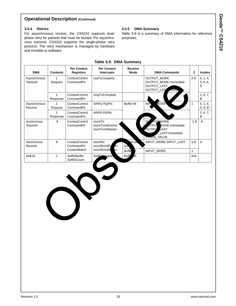
Revision 1.0 25 www.national.com
Geo
de™
CS
4210Operational Description (Continued)
3.5.4 RetriesFor asynchronous receive, the CS4210 supports dual-phase retry for packets that must be busied. For asynchro-nous transmit, CS4210 supports the single-phase retryprotocol. The retry mechanism is managed by hardwareand invisible to software.
3.5.5 DMA SummaryTable 3-9 is a summary of DMA information for referencepurposes.
Table 3-9. DMA Summary
DMA ContextsPer ContextRegisters
Per ContextInterrupts
ReceiveMode DMA Commands Z tcodes
AsynchronousTransmit
1Request
ContextControlCommandPtr
reqTxComplete OUTPUT_MOREOUTPUT_MORE-ImmediateOUTPUT_LASTOUTPUT_LAST-Immediate
2-8 0, 1, 4,5, 9, A,E
1Response
ContextControlCommandPtr
respTxComplete 2, 6, 7,B
AsynchronousReceive
1Request
ContextControlCommandPtr
ARRQ RQPkt Buffer-fill INPUT_MORE 1 0, 1, 4,5, 9, E*
1Response
ContextControlCommandPtr
ARRS RSPkt 2, 6, 7,B
IsochronousTransmit
8 ContextControlCommandPtr
IsochTxIsochTxIntEventnIsochTxIntMaskn
OUTPUT_MOREOUTPUT_MORE-ImmediateOUTPUT_LASTOUTPUT_LAST-ImmediateSTORE_VALUE
1-8 A
IsochronousReceive
8 ContextControlCommandPtrContextMatch
IsochRxIsochRxIntEventnIsochRxIntMaskn
Packet-per-buffer
INPUT_MORE INPUT_LAST 1-8 A
Buffer-fill INPUT_MORE 1
Self-ID 1 SelfIDBufferSelfIDCount
SelfIDComplete Buffer-fill N/A
Obsole
te

www.national.com 26 Revision 1.0
Geo
de™
CS
4210 Operational Description (Continued)
3.6 PHYSICAL REQUESTSWhen a block or quadlet read or write request is received,the CS4210 handles the operation automatically withoutinvolving software if the offset address in the requestpacket header meets a specific set of criteria listed below.Requests that do not meet these criteria are directed to theAR DMA Request context unless otherwise specified.CS4210 registers which are written via physical access tothe CS4210 yield unspecified results. The CS4210 checksto see if the offset address in the request packet header isone of the following.
If the offset falls within the physical range, then the offsetaddress is used as the memory address for the block orquadlet transaction. Physical range is defined by offsetsinclusively between a lower bound of 0h and an upperbound of 0000_FFFF_FFFFh. If the high order 16-bits ofthe offset address is 0000h, then the lower 32 bits of theoffset address are used as the memory address for theblock or quadlet transaction.
Lock transactions and block transactions with a non-zeroextended tcode are not supported in this address space,instead they are diverted to the AR DMA Request context.For read requests, the information needed to formulate theresponse packet is passed to the Physical Response Unit.Requests are only accepted if the source node ID of therequest has a corresponding bit in the AsynchronousRequest Filter registers and Physical Request Filter regis-ters (see Section 4.4.23 "Physical Request Filter Regis-ters" on page 79).
If the offset address selects one of the following addresses,the physical request unit directly handles quadlet compare-swaps and quadlet reads. Other requests are sent anack_type_error (see Table 3-7 on page 20.)
1) BUS_MANAGER_ID (FFFFF000021Ch):Local register is nscBusmgrID (BAR1+Offset 60h).
2) BANDWIDTH_AVAILABLE (FFFFF0000220h):Local register is nscBandwAvai (BAR1+Offset 64h).
3) CHANNELS_AVAILABLE_HI (FFFFF0000224h):Local register is nscChanAvailHi (BAR1+Offset 68h).
4) CHANNELS_AVAILABLE_LO (FFFFF0000228h):Local register is nscChanAvailLo (BAR1+Offset 6Ch).
If the offset address is one of the following addresses, thePhysical Request controller directly handles quadlet reads.Other requests shall be sent an ack_type_error.
1) Config ROM header (1st quadlet of the Config ROM)(FFFFF0000400h): Local register is ConfigROM-header (see Section 4.4.5 "Configuration ROM HeaderRegister" on page 61).
2) Bus ID (1st quadlet of the Bus_Info_Block)(FFFFF0000404h): Local register is BusID (see Sec-tion 4.4.6 "Bus Identification Register" on page 61).
3) Bus options (2nd quadlet of the Bus_Info_Block)(FFFFF0000408h): Local register is BusOptions (seeSection 4.4.7 "Bus Options Register" on page 62).
4) Global unique ID (3rd and 4th quadlets of theBus_Info_Block) (FFFFF000040Ch andFFFFF0000410h): Local registers are GlobalIDHi andGlobalIDLo (see Section 4.4.8 "Global Unique ID Reg-ister" on page 63).
5) Configuration ROM (FFFFF0000414h toFFFFF00007FFh). Mapped by the ConfigROMmap-ping register to a 1 KB block of system memory (seeSection 4.4.9 "Configuration ROM Mapping Register"on page 63)
For information about ack codes for write requests, seeSection 3.5.2 "Ack Codes for Write Requests" on page 24.
3.6.1 Filtering Physical RequestsSoftware can control which nodes it receives packets fromby utilizing the asynchronous filter registers. There are tworegisters, one for filtering out all requests from a specifiedset of nodes (AsynchronousRequestFilter register) and onefor filtering out physical requests from a specified set ofnodes (PhysicalRequestFilter register). The settings in bothregisters have a direct impact on how the AR DMARequest context is used (e.g., disabling only physicalreceives from a node causes all request packets from thatnode to be routed to the AR DMA Request context). Theusage and interrelationship between these registers isdescribed in Section 4.4.22 "Asynchronous Request FilterRegisters" on page 78.”Obsole
te

Revision 1.0 27 www.national.com
Geo
de™
CS
4210Operational Description (Continued)
3.6.2 Posted WritesFor write requests handled by the Physical Request con-troller, the CS4210 may send an ack_complete before thedata is actually written to system memory. These writes arereferred to as posted writes since posted writes impact thePhysical Request controller and the Asynchronous ReceiveRequest DMA context. Further information about postedwrites is located in Section 3.5.3 "Posted Writes" on page24. Information on host bus error handling of posted writesis provided in Section 3.7.7 "Posted Write Error" on page29.”
3.6.3 Physical ResponsesThe response packet generated for a physical read, non-posted write, and lock request contains the transactionlabel as it appeared in the request, the destination_ID asprovided in the request’s source_ID, and are transmitted atthe speed at which the request was received. The sourcebus ID in the response packet is equal to the destinationbus ID from the original request. Note that this is not neces-sarily the same as the contents of the busNumber field inthe Node ID register (BAR0+Offset E8h[15:6]). Unlike ARResponse packets, physical responses do not track aSPLIT_TIMEOUT expiration time.
3.6.4 Physical Response RetriesThere is a separate nibble-wide MaxPhysRespRetries fieldin the ATRetries Register (BAR0+Offset 08h[15:11]) thattells the Physical Response Unit how many times toattempt to retry the transmit operation for the responsepacket when an ack_busy* or ack_data_error is receivedfrom the target node. If the retry count expires, the packetis dropped and software is not notified. Refer to Section4.4.3 "ATRetries Register" on page 59 for register details.
3.6.5 Interrupt Considerations for Physical RequestsPhysical read request handling does not cause an interruptto be generated under any circumstances. Physical writerequests generate an interrupt when posted write process-ing yields an error. Lock requests to the serial bus registersgenerate an interrupt when the CS4210 is unable to delivera lock response packet.
3.6.6 Bus ResetOn a bus reset, all pending physical requests (those forwhich ack_pending was sent) are discarded. Following abus reset, only physical requests to the autonomous CSRresources (see Section 4.4.4 "Autonomous CSRResources" on page 60) can be handled immediately.Other physical requests are processed after software ini-tializes the filter registers (see Section 4.4.22 "Asynchro-nous Request Filter Registers" on page 78 and Section4.4.23 "Physical Request Filter Registers" on page 79).
Obsole
te
www.national.com 28 Revision 1.0
Geo
de™
CS
4210 Operational Description (Continued)
3.7 HOST BUS ERRORSThe CS4210 has three primary goals when dealing withhost bus error conditions:
1) Continue transmission and/or reception on all contextsnot involved in the error.
2) Provide information to software which is sufficient toallow recovery from the error when possible.
3) Provide a means of error recovery on a context otherthan a general chip reset.
3.7.1 Causes of Host Bus ErrorsHost bus errors can generally be classified as one of thefollowing:
• Addressing error (e.g., non-existent memory location)
• Operation error (e.g., attempt to write to read-onlymemory)
• Data transfer error (e.g., parity or unrecoverable ECC)
• Time-out error (e.g., reply on split transaction bus wasnot received in time)
Each of these errors can occur at three identifiable stagesin the processing of a descriptor:
• Descriptor fetch
• Data transfer (read or write)
• Optional descriptor status update.
In general, the nature of the bus error is not as significantas the stage of descriptor processing in which it occurs. Forexample, the difference between an addressing error and adata parity error is not significant to the error processing.
3.7.2 CS4210 Actions When Host Bus Error OccursWhen a host bus error occurs, the CS4210 performs adefined set of actions for all context types. Additionally,there is a set of actions that is performed depending on thecontext type. The following subsections outline theseactions.
3.7.2.1 Descriptor Read ErrorWhen an error occurs during the reading of a descriptor ordescriptor block, the behavior of the CS4210 is the sameregardless of the context type. The CS4210 sets Context-Control.dead and sets ContextControl.event toevt_descriptor_read to indicate that the descriptor fetchfailed. The unrecoverable error IntEvent is generated andthe context’s IntEvent is not set. Additionally, CommandPtris set to point to a descriptor within the descriptor block inwhich the error occurred. Since the descriptor could not beread, its xferStatus and resCount are not written with cur-rent values, and software must refer to ContextCon-trol.event for the status.
3.7.2.2 xferStatus Write ErrorFor any type of context, when the CS4210 encounters anerror writing the status to a descriptor, it sets ContextCon-trol.dead. The values that would have been written to xfer-Status of a descriptor are retained in ContextControl forinspection by system software. The unrecoverable errorIntEvent is generated and the context’s IntEvent is not setregardless of the setting of the interrupt (i) field in thedescriptor. Additionally, CommandPtr is set to point to adescriptor within the descriptor block in which the erroroccurred.
3.7.2.3 Transmit Data Read ErrorFor asynchronous request transmit, asynchronousresponse transmit, and isochronous transmit, the CS4210handles system data read errors in a similar manner. TheCS4210 does not stop processing for the context. Instead,the event code in the status of the OUTPUT_LAST*descriptor is set to indicate that there was an error and thenature of the error. The indicated errors are evt_data_reador evt_underrun. If the error occurs before a packet’sheader is placed in the output FIFO, the CS4210 canimmediately abort the packet transfer, optionally set thedescriptor status to evt_data_read or evt_underrun, andmove on to the next descriptor block. If the error occursafter the header has been placed in the output FIFO, theCS4210 stops placing data in the output FIFO. This causesthe CS4210 to send a packet with a length that does notagree with the data_length field of the header. If theCS4210 receives an ack_data_error from the addressednode, then the CS4210 substitutes evt_data_read orevt_underrun as appropriate. If the device returns anythingother than ack_data_error, then the CS4210 stores thatvalue in the status for the packet. This means that if theaddressed node returns an ack_pending on a block write,the error indication is lost.
If the packet was a broadcast write, an isochronous packet,or an asynchronous stream packet, no ack code is receivedfrom any node. In this case, the CS4210 assumes thatack_data_error was received and proceeds as outlinedabove.
Note: Underruns which occur due to host bus latency arenot construed to be host bus data errors, and as aresult such asynchronous request and responsepackets are retried as described in Section 4.4.3"ATRetries Register" on page 59.
Obsole
te

Revision 1.0 29 www.national.com
Geo
de™
CS
4210Operational Description (Continued)
3.7.3 Isochronous Transmit Data Write ErrorA data write error can occur when the CS4210 attempts towrite to the address indicated in a STORE_VALUE descrip-tor. This error is handled like a data read error with theexception that the event code is set to evt_data_write. TheCS4210 does not begin placing the packet associated witha STORE_VALUE into the output FIFO until theSTORE_VALUE operation is complete. This is to preventthe possibility of having multiple errors that cannot be prop-erly reported to system software.
3.7.4 Asynchronous Receive DMA Data Write ErrorWhen a host bus error occurs while the CS4210 is attempt-ing to write to either the request or response buffer, theCS4210 sets the corresponding ContextControl.dead andset ContextControl.event to evt_data_write. The unrecover-able error IntEvent is generated and the context’s IntEventis not set regardless of the setting of the interrupt (i) field inthe descriptor. CommandPtr.descriptorAddress points tothe descriptor that contained the buffer descriptor for thememory address at which the error occurred. Any data inthe input FIFO for the context is discarded.
3.7.5 Isochronous Receive Data Write ErrorIf a data write error occurs for a context that is in packet-per-buffer mode, the CS4210 sets ContextControl.event toevt_data_write or evt_overrun and conditionally updatesxferStatus of the descriptor in which the error occurred.Any remaining data in the input FIFO for the packet is dis-carded. The resCount value in a descriptor that has anerror will not necessarily reflect the correct number of databytes successfully written to memory. If a FIFO overrunoccurs for a context that is in buffer-fill mode, the packet istreated as if a data length error had occurred and is‘backed out’ of the receive buffer (xferStatus and resCountnot updated) and the remainder of the packet is discardedfrom the input FIFO. If a host bus error occurs for a contextin buffer-fill mode, the CS4210 sets ContextControl.deadand sets ContextControl.event to evt_data_write. The unre-coverable error IntEvent is generated and the context’sIntEvent is not set regardless of the setting of the interrupt(i) field in the descriptor. CommandPtr.descriptorAddresspoints to the descriptor that contained the buffer descriptorfor the memory address at which the error occurred. Anydata in the input FIFO for the context is discarded.
3.7.6 Physical Read ErrorWhen an external node does a physical access and theCS4210’s read of system memory fails, the CS4210returns an error indication to the requester by forming aresponse containing a response code of resp_data_error. Ifthe device replies with ack_busy or ack_data_error the hostretries the packet. If the error was caused by a FIFO under-run, the CS4210 retries with the same response. If theerror was a host bus error, the response packet is changedto resp_data_error.
3.7.7 Posted Write ErrorWhether to be handled by the Physical Request controlleror by the Asynchronous Receive Request context, writerequests to certain address ranges (see Section 3.6 "Phys-ical Requests" on page 26) may be acked withack_complete before the data is actually written to systemmemory. Since the sending node has been notified that theaction is complete, when the CS4210 cannot complete aposted write operation due to a host bus error the systemmust be notified so that software can recover.
If an error occurs in writing the posted data packet, then theCS4210 sets the IntEvent.PostedWriteErr bit (BAR0+Offset80h[8]) to indicate that an error has occurred and the writeremains pending. Software can then read the source nodeID and offset address from the PostedWriteAddress regis-ter and then clear IntEvent.PostedWriteErr. When softwareclears IntEvent.PostedWriteErr, that write is no longerpending.
Although the CS4210 allows four pending writes, errorreporting is through a single pair of software visible regis-ters. If multiple posted write failures have occurred, soft-ware accesses them one at a time through thePostedWriteAddress register. When software clearsIntEvent.PostedWriteErr, this is a signal to the CS4210 thatsoftware has completed reading of the current contents ofPostedWriteAddress and that the CS4210 can reportanother error by again setting IntEvent.PostedWriteErr andpresenting a new set of values when software reads Post-edWriteAddress. Table 3-10 provides a map of the Posted-WriteAddress register. Refer to Section 4.4.10"PostedWriteAddress Register" on page 64 for further reg-ister information.
If the CS4210 has four pending physical writes, additionalphysical writes may not be posted. Instead the CS4210returns ack_pending and only returns a complete indicationwhen the write is actually done.
Table 3-10. BAR0+Offset 38h: PostedWriteAddress Register Map
31 30 29 28 27 26 25 24 23 22 21 20 19 18 17 16 15 14 13 12 11 10 9 8 7 6 5 4 3 2 1 0
sourceID offsetHi
offsetLo
Obsole
te

www.national.com 30 Revision 1.0
Geo
de™
CS
4210 Operational Description (Continued)
3.8 BUS RESETSWhen a 1394 bus reset occurs, certain actions must betaken by software for proper operation of the DMA con-texts. These actions and the behavior of the CS4210 aredescribed in the following subsections.
3.8.1 Asynchronous TransmitUpon detection of a bus reset, the CS4210 ceases trans-mission of asynchronous transmit packets. When thisoccurs there are two possibilities for AT packets that are leftin the FIFO.
• Case 1 is when a bus reset occurs after the packet wastransmitted but before an ack was received. For thiscategory, the link side of the CS4210 returnsevt_missing_ack.
• Case 2 is when a bus reset occurs after the packet isplaced in the FIFO but before it is transmitted. For thiscategory, the link side of the CS4210 returnsevt_flushed.
When each context becomes stable (all data transfers havebeen halted and status writes have been completed), theCS4210 clears the corresponding ContextControl.activebit.
When a bus reset occurs, the link side flushes the asyn-chronous transmit FIFO(s) until the IntEvent.busReset con-dition is cleared. Software must make sure thatIntEvent.busReset is not cleared until:
1) software has cleared the ContextControl.run bits forboth Asynchronous Transmit contexts, and
2) both Asynchronous Transmit contexts have acqui-esced and both ContextControl.active fields are zero.This is to ensure that all queued asynchronous pack-ets (with potentially stale node numbers) are flushed.
Once the contexts are no longer active, software may clearthe busReset interrupt condition, and hardware stops flush-ing the asynchronous transmit FIFO(s). Before setting Con-textControl.run for either context following a bus reset,software must ensure that NodeID.iDValid is set and thatNodeID.nodeNumber (Section 4.4.19 "Node ID and StatusRegister" on page 76) does not equal 63.
3.8.2 Asynchronous ReceiveTo assist software in determining which asynchronousrequest packets arrived before and after a bus reset, this isnecessary since node numbers may have changed, theCS4210 inserts a synthesized CS4103 packet into the ARDMA Request Context buffer (if active) as soon as a busreset condition is detected. The format of the packet can befound in the 1394 OHCI specification.
Software can distinguish the bus-reset packet from authen-tic CS4103 packets by the value of eventCode which is setto evt_bus_reset. Software can further interpret and coordi-nate received asynchronous packets across multiple busresets by using the selfIDGeneration number provided inthe bus-reset packet. Since the bus-reset packet is fabri-cated when a bus reset is initially detected, the selfIDGen-eration number is for the new (not previous) generation andis the same as the selfIDGeneration number in the SelfID-Count register as well as in the selfID buffer. If more thanone bus reset has occurred without any intervening pack-ets, then only the “last” one is required to result in a synthe-sized bus-reset packet. If the input FIFO is full when a busreset occurs, the link side of the FIFO inserts the bus-resetpacket when space becomes available. If the AR DMArequest context does not have enough buffer space for thebus-reset packet, the packet is synthesized once bufferspace becomes available. The bus reset interrupt(IntEvent.busReset) is independent on the time when thispacket goes from the FIFO into a host buffer. This interruptshall occur as soon as possible after a bus reset has beendetected. The bus-reset packet is no different from anyother packet going into the AR Request buffer in thatIntEvent.RQPkt is generated like it is for other packets.
3.8.3 Isochronous Transmit and ReceiveBus reset does not affect isochronous contexts.
Obsole
te

Revision 1.0 31 www.national.com
Geo
de™
CS
4210Operational Description (Continued)
3.9 SERIAL EEPROMA serial EEPROM may be used to configure the CS4210. Ifa serial EEPROM device is connected, the CS4210 detectsthe pull-up resistor on the EEDATA pin (pin 5) and consid-ers the EEPROM present. Immediately after RST# is deas-serted, the serial EEPROM is scanned via EEDATA andEECLK (pin 4). The CS4210 reads configuration informa-tion from the first 34 bytes of the EEPROM.
If the presence of the serial EEPROM was not detected,the CS4210 will not attempt to load configuration data viathe EEDATA/EECLK pins. It will instead allow software towrite to the guidHi and guidLo bit fields of the GUID regis-ter once after each hardware reset (RST#).
3.9.1 Serial EEPROM Cyclic Redundancy CheckThe serial EEPROM uses a Cyclical Redundancy Check(CRC) to insure the data in the EEPROM is valid. If theCRC check fails, the data from the EEPROM is not loadedinto the mapped registers listed in Table 3-11. The CRC1and CRC2 values may be computed using the samplecode in Figure 3-1 "CRC1 and CRC2 Sample Code" onpage 32. This code accepts hexadecimal data from STDINand writes data plus CRC to STDOUT. As a check, thiscode should produce the results as shown in Figure 3-1.
Table 3-11. Serial EEPROM Map
Offset Description
00h subsystem[7:0]
01h subsystem[15:8]
02h subsystem[23:16]
03h subsystem[31:24]
04h configROMheader[7:0]
05h configROMheader[15:8]
06h configROMheader[23:16]
07h configROMheader[31:24]
08h busOptions[7:0]
09h busOptions[15:8]
0Ah busOptions[23:16]
0Bh busOptions[31:24]
0Ch guidHi[7:0]
0Dh guidHi[15:8]
0Eh guidHi[23:16]
0Fh guidHi[31:24]
10h guidLo[7:0]
11h guidLo[15:8]
12h guidLo[23:16]
13h guidLo[31:24]
14h nscControl[7:0]
15h nscControl[15:8]
16h nscControl[23:16]
17h nscControl[31:24]
18h nscTxThrsh[7:0]
19h nscTxThrsh[15:8]
1Ah nscTxThrsh[23:16]
1Bh nscTxThrsh[31:24]
1Ch cmcControl[7:0]
1Dh cmcControl[15:8]
1Eh cmcControl[23:16]
1fh cmcControl[31:24]
20h CRC1
21h CRC2
Obsole
te

www.national.com 32 Revision 1.0
Geo
de™
CS
4210 Operational Description (Continued)
Figure 3-1. CRC1 and CRC2 Sample Code
ff ff ff ff ff ff ff ff -> CRC1 = feh, CRC2 = 70h01 23 45 67 89 ab cd ef -> CRC1 = 19h, CRC2 = 07h00 00 00 00 00 00 00 00 -> CRC1 = bfh, CRC2 = f4h#include <stdio.h>typedef unsigned char uchar_t;typedef unsigned short ushort_t;typedef unsigned long long_t;
ushort_t calc_crc(ushort_t r, uchar_t d);ushort_t rev16(ushort_t src);/* main routine */int main(int argc, char *argv[]){
ushort_t residual = 0xffff;int din;uchar_t byte;uchar_t crc1, crc2;while(scanf("%2x", &din ) != EOF ) {
byte = din;printf("%2.2x ", byte);residual = calc_crc(residual, byte);
};printf("\n");residual = rev16(residual);crc1 = ~(residual & 0x00ff);crc2 = ~(residual>>8);printf("CRC1 = %2.2hxh\n", crc1);printf("CRC2 = %2.2hxh\n", crc2);
return(0);/* calc_crc - apply a byte of data to the 16-bit CRC */}
ushort_t calc_crc(ushort_t r, uchar_t d){
ushort_t bit_in;int i;
for(i=0;i<8;i++) {bit_in = (d>>i) & 0x0001;if((r>>15) ^ bit_in)
r = (((r<<1) & 0x7ffb) | ((r>>15 ^ ((r>>14)&0x0001) ^ bit_in) << 15) |((r>>15 ^ ((r>>1)&0x0001) ^ bit_in) << 2) | 0x0001 );
elser <<= 1;
}return(r);
}
ushort_t rev16(ushort_t src){
return(((src&0x0001)<<15) |((src&0x0002)<<13) |((src&0x0004)<<11) |((src&0x0008)<<9) |((src&0x0010)<<7) |((src&0x0020)<<5) |((src&0x0040)<<3) |((src&0x0080)<<1) |((src&0x0100)>>1) |((src&0x0200)>>3) |((src&0x0400)>>5) |((src&0x0800)>>7) |((src&0x1000)>>9) |((src&0x2000)>>11) |((src&0x4000)>>13) |((src&0x8000)>>15);
}
Obsole
te
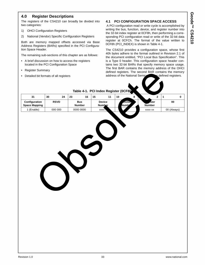
Revision 1.0 33 www.national.com
Geo
de™
CS
42104.0 Register DescriptionsThe registers of the CS4210 can broadly be divided intotwo categories:
1) OHCI Configuration Registers
2) National (Vendor) Specific Configuration Registers
Both are memory mapped offsets accessed via BaseAddress Registers (BARs) specified in the PCI Configura-tion Space Header.
The remaining sub-sections of this chapter are as follows:
• A brief discussion on how to access the registerslocated in the PCI Configuration Space
• Register Summary
• Detailed bit formats of all registers
4.1 PCI CONFIGURATION SPACE ACCESSA PCI configuration read or write cycle is accomplished by
writing the bus, function, device, and register number intothe 32-bit index register at 0CF8h, then performing a corre-sponding PCI configuration read or write of the 32-bit dataregister at 0CFCh. The format of the value written to0CF8h (PCI_INDEX) is shown in Table 4-1.
The CS4210 provides a configuration space, whose first40h bytes adhere to the format outlined in Revision 2.1 ofthe document entitled, “PCI Local Bus Specification”. Thisis a Type 0 header. This configuration space header con-tains two 32-bit BARs that specify memory space usage.The first BAR contains the memory address of the OHCIdefined registers. The second BAR contains the memoryaddress of the National Semiconductor defined registers.
Table 4-1. PCI Index Register (0CF8h)
31 30 24 23 16 15 11 10 8 7 2 1 0
ConfigurationSpace Mapping
RSVD BusNumber
DeviceNumber
FunctionNumber
RegisterNumber
00
1 (Enable) 000 000 0000 0000 xxxx x xxx xxxx xx 00 (Always)
Obsole
te

www.national.com 34 Revision 1.0
Geo
de™
CS
4210 Register Descriptions (Continued)
4.2 REGISTER SUMMARYThe tables in this subsection summarize all the registers ofthe CS4210. Included in the tables are the register’s reset
values and page references where the bit formats arefound.
Table 4-2. PCI Configuration Registers Summary
IndexWidth(Bits) Access Name Reset Value
Reference(Page)
00h-01h 16 R Vendor Identification Register 1000h Page 42
02h-03h 16 R Device Identification Register 000Fh Page 42
04h-05h 16 RW PCI Command Register 0000h Page 42
06h-07h 16 RW PCI Status Register 0200h Page 43
08h 8 R Device Revision ID Register 03h Page 43
09h-0Bh 24 R PCI Class Code Register 0C0010h Page 43
0Ch 8 R PCI Cache Line Size Register 00h Page 43
0Dh 8 RW PCI Latency Timer Register 50h Page 43
0Eh 8 R PCI Header Type Register 00h Page 43
0Fh 8 R PCI BIST Register 00h Page 43
10h-13h 32 RW Base Address Register 0 (BAR0): Sets base address formemory mapped OHCI Configuration Registers
00000000h Page 44
14h-17h 32 RW Base Address Register 1 (BAR1): Sets base address formemory mapped National Semiconductor device specificoperational registers.
00000000h Page 44
18h-2B -- -- Reserved --- Page 44
2Ch-2Dh 16 R Subsystem Vendor Identification Register 1 Page 44
2Eh-2Fh 16 R Subsystem Identification Register 2 Page 44
30h-33h -- -- Reserved --- Page 44
34h 8 R Capabilities Pointer Register 3 Page 45
35h-3Bh -- -- Reserved --- Page 45
3Ch 8 RW Interrupt Line Register FFh Page 45
3Dh 8 R Interrupt Pin Register 01h Page 45
3Eh 8 R Min Grant Register 00h Page 45
3Fh 8 R Max Latency Register 00h Page 45
40h-43h 32 RW PCI HCI Control Register 00h Page 45
44h 8 R Capability ID Register 01h Page 45
45h 8 R Next Item Pointer Register 00h Page 45
46h-47h 16 R Power Management Capabilities Register 4 Page 46
48h-49h 16 R/W Power Management and Control Status Register 5 Page 46
4Ah 8 R Power Management CSR Bridge SupportExtension Register
00h Page 47
4Bh 8 R Power Management Data Register 00h Page 47
1. The reset value must be set in the serial EEPROM to the vendor identification number assigned by the PCI SIG.2. The reset value must be set in serial EEPROM to a unique number chosen by the user to represent this PCI device implementation.3. The reset value is dependent upon the PCICapabilities bit in the nscControl register (BAR1+Offset 00h[20]) which can be configured
by the serial EEPROM. If enabled in the EEPROM, the reset value of the register is 44h. If not enabled in the EEPROM or if no EE-PROM is present, then the reset value is 00h.
4. The reset value is dependent upon the PCICapabilities bit in the nscControl register (BAR1+Offset 00h[20]) which can be configuredby serial EEPROM. If enabled in the EEPROM the reset value of this register is 4000h. If not or if no EEPROM is present, then thereset value is 000h.
5. The reset value is dependent upon the PCICapabilities bit in the nscControl register (BAR1+Offset 00h[20]) which can be configuredby serial EEPROM. If enabled in the EEPROM the reset value of this register is 8000h. If not or if no EEPROM is present then the resetvalue is 000h.
Obsole
te

Revision 1.0 35 www.national.com
Geo
de™
CS
4210Register Descriptions (Continued)
Table 4-3. OHCI Configuration Registers Summary
BAR0+OffsetWidth(Bits) Access Name Reset Value
Reference(Page)
00h-03h 32 R Version Register xxh Page 58
04h-07h 32 RSU/RU GUIDROM Register xxh Page 58
08h-0Bh 32 RW ATRetries Register xxh Page 59
0Ch-0Fh 32 RWU CSRReadData Register xxh Page 60
10h-13h 32 RW CSRCompareData Register xxh
14h-17h 32 RW CSRControl Register 800xh
18h-1Bh 32 RWU Configuration ROM Header Register 00h Page 61
1Ch-1Fh 32 R Bus Identification Register 31333934h Page 61
20h-23h 32 RW Bus Options Register xxh Page 62
24h-27h 32 RW GUIDHi Register xxh Page 63
28h-2Bh 32 R/W GUIDLo Register xxh
2Ch-33h -- -- Reserved 00h --
34h-37h 32 RW Configuration ROM Map Register xxh Page 63
38h-3Bh 32 RU PostedWriteAddressLo Register xxh Page 64
3Ch-3Fh 32 RU PostedWriteAddressHi Register xxh
40h-43h 32 R Vendor ID Register 80017h Page 64
50h-53h 32 RSC HCControl Set Register xxh Page 65
54h-57h 32 RSC HCControl Clear Register xxh
58h-63h -- -- Reserved 00h --
64h-67h 32 RW Self-ID Buffer Pointer Register xxh Page 68
68h-6Bh 32 RU Self-ID Count Register xxh Page 68
70h-73h 32 RSC IRMultiChanMaskHi Set Register xxh Page 69
74h-77h 32 RSC IRMultiChanMaskHi Clear Register xxh
78h-7Bh 32 RSC IRMultiChanMaskLo Set Register xxh
7Ch-7Fh 32 RSC IRMultiChanMaskLo Clear Register xxh
80h-83h 32 RSCU IntEvent Set Register xxh Page 70
84h-87h 32 RSCU IntEvent Clear Register xxh
88h-8Bh 32 RSCU IntMask Set Register xxh Page 72
8Ch-8Fh 32 RSCU IntMask Clear Register xxh
90h-93h 32 RSC IsochTxIntEvent Set Register xxh Page 73
94h-97h 32 RSC IsochTxIntEvent Clear Register xxh
98h-9Bh 32 RSC IsochTxIntMask Set Register xxh Page 73
9Ch-9Fh 32 RSC IsochTxIntMask Clear Register xxh
A0h-A3h 32 RSC IsochRxIntEvent Set Register xxh Page 74
A4h-A7h 32 RSC IsochRxIntEvent Clear Register xxh
A8h-ABh 32 RSC IsochRxIntMask Set Register xxh Page 74
ACh-AFh 32 RSC IsochRxIntMask Clear Register xxh
B0h-DBh -- -- Reserved 00h --
DCh-DFh 32 RW Fairness Control Register xxh Page 75
E0h-E3h 32 RSC LinkControl Set Register xxh Page 75
E4h-E7h 32 RSC LinkControl Clear Register xxh
E8h-EBh 32 RU Node ID and Status Register xxh Page 76
ECh-EFh 32 RWU PHYControl Register xxh Page 77
F0h-F3h 32 RWU IsochCycleTimer Register xxh Page 77
F4h-FFh -- -- Reserved 00h --
100h-103h 32 RSCU AsyncRequestFilterHi Set Register 00h Page 78
104h-107h 32 RSCU AsyncRequestFilterHi Clear Register 00h
Obsole
te

www.national.com 36 Revision 1.0
Geo
de™
CS
4210 Register Descriptions (Continued)
108h-10Bh 32 RSCU AsyncRequestFilterLo Set Register 00h Page 78
10Ch-10Fh 32 RSCU AsyncRequestFilterLo Clear Register 00h
110h-113h 32 RSCU PhysicalRequestHi Set Register 00h Page 79
114h-117h 32 RSCU PhysicalRequestHi Clear Register 00h
118h-1Bh 32 RSCU PhysicalRequestLo Set Register 00h Page 79
11Ch-11Fh 32 RSCU PhysicalRequestLo Clear Register 00h
180h-183h 32 RSU AsyncReqTxContextControl Set Register xxh Page 80
184h-187h 32 RSU AsyncReqTxContextControl Clear Register xxh
188h-18Bh -- -- Reserved 00h --
18Ch-18Fh 32 AsyncReqTxCommandPtr Register xxh Page 80
190h-19Fh -- -- Reserved 00h --
1A0h-1A3h 32 RSCU/RU AsyncRespTxContextControl Set Register xxh Page 81
1A4h-1A7h 32 RSCU/RU AsyncRespTxContextControl Clear Register xxh
1ACh-1AFh 32 RWU AsyncRespTxCommandPtr Register xxh Page 81
1B0h-1BFh -- -- Reserved 00h --
1C0h-1C3h 32 RSCU/RSU AsyncReqRxContextControl Set Register xxh Page 82
1C4h-1C7h 32 AsyncReqRxContextControl Clear Register xxh
1C8h-1CBh -- -- Reserved 00h --
1CCh-1CFh 32 AsyncReqRxCommandPtr Register xxh Page 82
1D0h-1DFh -- -- Reserved 00h --
1E0h-1E3h 32 RSCU/RU AsyncRespRxContextControl Set Register xxh Page 83
1E4h-1E7h 32 RSCU/RU AsyncRespRxContextControl Clear Register xxh
1E8h-1EBh -- -- Reserved 00h --
1ECh-1EFh 32 RWU AsyncRespRxCommandPtr Register xxh Page 83
200h-203h 32 RSCU/RSU IsochTx0ContextControl Set Register xxh Page 85
204h-207h 32 RSCU/RSU IsochTx0ContextControl Clear Register xxh
208h-20Bh -- -- Reserved 00h --
20Ch-20Fh 32 RWU IsochTx0CommandPtr Register xxh Page 85
210h-213h 32 RSCU/RSU IsochTx1ContextControl Set Register xxh Page 85
214h-217h RSCU/RSU IsochTx1ContextControl Clear Register xxh
218h-21Bh -- -- Reserved 00h --
21Ch-21Fh 32 RWU IsochTx1CommandPtr Register xxh Page 85
220h-223h 32 RSCU/RSU IsochTx2ContextControl Set Register xxh Page 85
224h-227h 32 RSCU/RSU IsochTx2ContextControl Clear Register xxh
228h-22Bh -- -- Reserved 00h --
22Ch-22Fh 32 RWU IsochTx2CommandPtr Register xxh Page 85
230h-233h 32 RSCU/RSU IsochTx3ContextControl Set Register xxh Page 85
234h-237h 32 RSCU/RSU IsochTx3ContextControl Clear Register xxh
238h-23Bh -- -- Reserved 00h --
23Ch-23Fh 32 RWU IsochTx3CommandPtr Register xxh Page 85
240h-243h 32 RSCU/RSU IsochTx4ContextControl Set Register xxh Page 85
244h-247h 32 RSCU/RSU IsochTx4ContextControl Clear Register xxh
248h-24Bh -- -- Reserved 00h --
24Ch-24Fh 32 RWU IsochTx4CommandPtr Register xxh Page 85
250h-253h 32 RSCU/RSU IsochTx5ContextControl Set Register xxh Page 85
254h-257h 32 RSCU/RSU IsochTx5ContextControl Clear Register xxh
258h-25Bh -- -- Reserved 00h --
25Ch-25Fh 32 RWU IsochTx5CommandPtr Register xxh Page 85
Table 4-3. OHCI Configuration Registers Summary (Continued)
BAR0+OffsetWidth(Bits) Access Name Reset Value
Reference(Page)
Obsole
te

Revision 1.0 37 www.national.com
Geo
de™
CS
4210Register Descriptions (Continued)
260h-263h 32 RSCU/RSU IsochTx6ContextControl Set Register xxh Page 85
264h-267h 32 RSCU/RSU IsochTx6ContextControl Clear Register xxh
268h-26Bh -- -- Reserved 00h --
26Ch-26Fh 32 RWU IsochTx6CommandPtr Register xxh Page 85
270h-273h 32 RSCU/RSU IsochTx7ContextControl Set Register xxh Page 85
274h-277h 32 RSCU/RSU IsochTx7ContextControl Clear Register xxh
278h-27Bh -- -- Reserved 00h --
27Ch-27Fh 32 RWU IsochTx7CommandPtr Register xxh Page 85
280h-3FFh -- -- Reserved 00h --
400h-403h 32 RSCU/RSU IsochRx0ContextControl Set Register xxh Page 87
404h-407h 32 RSCU/RSU IsochRx0ContextControl Clear Register xxh
408h-40Bh -- -- Reserved 00h --
40Ch-40Fh 32 RWU IsochRx0CommandPtr Register xxh Page 88
410h-413h 32 RW IsochRx0ContextMatch xxh Page 88
414h-41Fh -- -- Reserved 00h --
420h-423h 32 RSCU/RSU IsochRx1ContextControl Set Register xxh Page 87
424h-427h 32 RSCU/RSU IsochRx1ContextControl Clear Register xxh
428h-42Bh -- -- Reserved 00h --
42Ch-42Fh 32 RWU IsochRx1CommandPtr Register xxh Page 88
430h-433h 32 RW IsochRx1ContextMatch Register xxh Page 88
434h-43Fh -- -- Reserved 00h --
440h-443h 32 RSCU/RSU IsochRx2ContextControl Set Register xxh Page 87
444h-447h 32 RSCU/RSU IsochRx2ContextControl Clear Register xxh
448h-44Bh -- -- Reserved 00h --
44Ch-44Fh 32 RWU IsochRx2CommandPtr Register xxh Page 88
450h-453h 32 RW IsochRx2ContextMatch Register xxh Page 88
454h-45Fh -- -- Reserved 00h --
460h-463h 32 RSCU/RSU IsochRx3ContextControl Set Register xxh Page 87
464h-467h 32 RSCU/RSU IsochRx3ContextControl Clear Register xxh
468h-46Bh -- -- Reserved 00h --
46Ch-46Fh 32 RWU IsochRx3CommandPtr Register xxh Page 88
470h-473h 32 RW IsochRx3ContextMatch Register xxh Page 88
474h-47Fh -- -- Reserved 00h --
480h-483h 32 RSCU/RSU IsochRx4ContextControl Set Register xxh Page 87
484h-487h 32 RSCU/RSU IsochRx4ContextControl Clear Register xxh
488h-48Bh -- -- Reserved 00h --
48Ch-48Fh 32 RWU IsochRx4CommandPtr Register xxh Page 88
490h-493h 32 RW IsochRx4ContextMatch Register xxh Page 88
494h-49Fh -- -- Reserved 00h --
4A0h-403h 32 RSCU/RSU IsochRx5ContextControl Set Register xxh Page 87
4A4h-407h 32 RSCU/RSU IsochRx5ContextControl Clear Register xxh
4A8h-40Bh -- -- Reserved 00h --
4ACh-40Fh 32 RWU IsochRx5CommandPtr Register xxh Page 88
4B0h-413h 32 RW IsochRx5ContextMatch Register xxh Page 88
4B4h-41Fh -- -- Reserved 00h --
4C0h-4C3h 32 RSCU/RSU IsochRx6ContextControl Set Register xxh Page 87
4C4h-4C7h 32 RSCU/RSU IsochRx6ContextControl Clear Register xxh
4C8h-4CBh -- -- Reserved 00h --
Table 4-3. OHCI Configuration Registers Summary (Continued)
BAR0+OffsetWidth(Bits) Access Name Reset Value
Reference(Page)
Obsole
te

www.national.com 38 Revision 1.0
Geo
de™
CS
4210 Register Descriptions (Continued)
4CCh-4CFh 32 RWU IsochRx6CommandPtr Register xxh Page 88
4D0h-4D3h 32 RW IsochRx6ContextMatch Register xxh Page 88
4D4h-4DFh -- -- Reserved 00h --
4E0h-4E3h 32 RSCU/RSU IsochRx7ContextControl Set Register xxh Page 87
4E4h-4E7h 32 RSCU/RSU IsochRx7ContextControl Clear Register xxh
4E8h-4EBh -- -- Reserved 00h --
4ECh-4EFh 32 RWU IsochRx7CommandPtr Register xxh Page 88
4F0h-4F3h 32 RW IsochRx7ContextMatch Register xxh Page 88
4F4h-4FFh -- -- Reserved 00h --
Table 4-3. OHCI Configuration Registers Summary (Continued)
BAR0+OffsetWidth(Bits) Access Name Reset Value
Reference(Page)
Obsole
te

Revision 1.0 39 www.national.com
Geo
de™
CS
4210Register Descriptions (Continued)
Table 4-4. National Specific Configuration Registers Summary
BAR1+OffsetWidth(Bits) Access Name Reset Value
Reference(Page)
00h-03h 32 RW nscControl Register 00h Page 91
04h-07h 32 RSCU nscEvent Set Register xxh Page 93
08h-0Bh 32 RSCU nscEvent Clear Register xxh
0Ch-0Fh 32 RSC nscEventMask Set Register xxh Page 93
10h-13h 32 RSC nscEventMask Clear Register xxh
14h-17h 32 RU/RW nscRAMBist Register xxh Page 94
18h-1Bh 32 RW nscCmcControl Register 00h Page 94
20h-23h 32 RW/RU nscTxThreshold Register 01FE01FEh Page 94
24h-27h 32 RW nscSubSystem Register 00h Page 94
40h-43h 32 RW nscPhysReadCount Register 00h Page 95
44h-47h 32 RW nscPhysWriteCount Register 00h Page 95
48h-4Bh 32 RW nscPhysLockCount Register 00h Page 95
4Ch-5Fh -- -- Reserved 00h --
60h-63h 32 R nscBusmgrID Register xxh Page 96
64h-67h 32 R nscBandwAvail Register xxh Page 96
68h-6Bh 32 R nscChanAvailHi Register xxh Page 96
6Ch-6Fh 32 R nscChanAvailLo Register xxh Page 96
Obsole
te
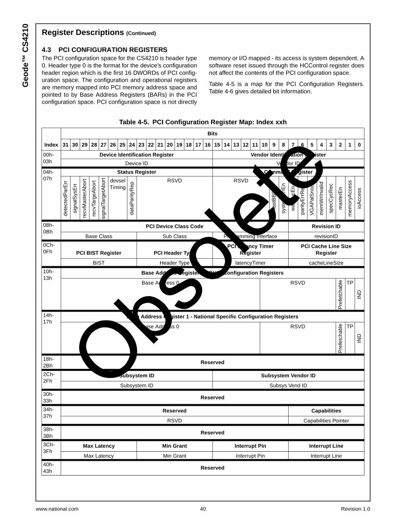
www.national.com 40 Revision 1.0
Geo
de™
CS
4210 Register Descriptions (Continued)
4.3 PCI CONFIGURATION REGISTERSThe PCI configuration space for the CS4210 is header type0. Header type 0 is the format for the device’s configurationheader region which is the first 16 DWORDs of PCI config-uration space. The configuration and operational registersare memory mapped into PCI memory address space andpointed to by Base Address Registers (BARs) in the PCIconfiguration space. PCI configuration space is not directly
memory or I/O mapped - its access is system dependent. Asoftware reset issued through the HCControl register doesnot affect the contents of the PCI configuration space.
Table 4-5 is a map for the PCI Configuration Registers.Table 4-6 gives detailed bit information.
Table 4-5. PCI Configuration Register Map: Index xxh
Index
Bits
31 30 29 28 27 26 25 24 23 22 21 20 19 18 17 16 15 14 13 12 11 10 9 8 7 6 5 4 3 2 1 0
00h-03h
Device Identification Register Vendor Identification Register
Device ID Vendor ID
04h-07h
Status Register Command Register
dete
cted
Par
Err
sign
alS
ysE
rr
recv
Mas
terA
bort
recv
Targ
eAbo
rt
sign
alTa
rget
Abo
rt devselTiming
data
Par
ityR
ep
RSVD RSVD
fast
BB
En
syst
emE
rrE
n
wai
tCyc
En
parit
yErr
Res
p
VG
AP
alS
noop
mem
WrI
nval
id
spec
Cyc
Rec
mas
terE
n
mem
oryA
cces
s
ioA
cces
s
08h-0Bh
PCI Device Class Code Revision ID
Base Class Sub Class Programming Interface revisionID
0Ch-0Fh PCI BIST Register PCI Header Type
PCI Latency TimerRegister
PCI Cache Line SizeRegister
BIST Header Type latencyTimer cacheLineSize
10h-13h
Base Address Register 0 - OHCI Configuration Registers
Base Address 0 RSVD
Pre
fetc
habl
e TP
IND
14h-17h
Base Address Register 1 - National Specific Configuration Registers
Base Address 0 RSVD
Pre
fetc
habl
e TP
IND
18h-2Bh
Reserved
2Ch-2Fh
Subsystem ID Subsystem Vendor ID
Subsystem ID Subsys Vend ID
30h-33h
Reserved
34h-37h
Reserved Capabilities
RSVD Capabilities Pointer
38h-3Bh
Reserved
3Ch-3Fh
Max Latency Min Grant Interrupt Pin Interrupt Line
Max Latency Min Grant Interrupt Pin Interrupt Line
40h-43h
Reserved
Obsole
te

Revision 1.0 41 www.national.com
Geo
de™
CS
4210Register Descriptions (Continued)
44h-47h
Power Management Capabilities Next Item Pointer Capability ID
pmeSupport
d2S
uppo
rt
daS
uppo
rt
dynD
ata
RS
VD
DS
I
auxP
ower
pmeC
LK
pmV
ersi
on NextItemPointer CapabilityID
48h-4Bh Power Management Data
Power Management CSRBride Support Extensions Power Management Control and Status
pmData pmcrBSE
pmeS
tatu
s dynData
pmeE
nab RSVD
dynD
ataE
nab RSVD
pmeS
tate
Table 4-5. PCI Configuration Register Map: Index xxh (Continued)
Index
Bits
31 30 29 28 27 26 25 24 23 22 21 20 19 18 17 16 15 14 13 12 11 10 9 8 7 6 5 4 3 2 1 0
Obsole
te

www.national.com 42 Revision 1.0
Geo
de™
CS
4210 Register Descriptions (Continued)
Table 4-6. PCI Configuration Register Definitions
Bit Name Access Reset Description
Index 00h Vendor Identification Register
15:0 Vendor ID RO 1000h Vendor Identification: This register identifies the manufacturer of theCS4210 as National Semiconductor.
Index 02h Device Identification Register
15:0 Device ID RO 000Fh Device Identification: This register identifies the CS4210 as the IEEE1394 Open Host Controller.
Index 04h PCI Command Register
This register provides coarse control over the device’s ability to generate and respond to PCI cycles. It is required that the CS4210 sup-port both PCI bus-mastering and memory-mapping of all configuration and operational registers into the memory address space of thePC host. Consequently, the fields memoryAccess and masterEn should always be set to 1 during device configuration.
Once the CS4210 starts processing DMA descriptor lists, the action of resetting either field memoryAccess or masterEn to 0 halts allPCI operations. If the field memoryAccess is reset to 0, the CS4210 can no longer respond to any software command addressed to itand interrupt generation is halted.
15:10 RSVD --- 000000 Reserved
9 fastBBEn RO 0 Fast Back-to-Back Enable: This function is not supported and is alwaysdisabled. 0 = Disable; 1 = Enable.
8 systemErrEn R/W 0 System Error Enable: Allow assertion on detection of special errors. 0 =Disable; 1 = Enable.
7 waitCycEn RO 0 Wait Cycle Control: This function is not supported and is always disabled.0 = Disable; 1 = Enable.
6 parityErrResp R/W 0 Parity Error Response: Allow the CS4210 to drive PERR# when a parityerror is detected. 0 = Disable; 1 = Enable.
5 VGAPalSnoop RO 0 VGA Palette Snoop: This function is not supported, Is is always disabled. 0= Disable; 1 = Enable.
4 memWrInvalid RO 0 Memory Write and Invalidate: Allow the CS4210 to do memory write andinvalidate cycles. 0 = Disable; 1 = Enable.
If disabled, memory write commands must be used.
3 specCycRec RO 0 Special Cycles: This function is not supported and is always disabled. 0 =Disable; 1 = Enable.
2 masterEn R/W 0 Bus Master: Allow the CS4210 bus mastering capabilities.0 = Disable; 1 = Enable.
1 memoryAccess R/W 0 Memory Space Access: Allow the CS4210 to respond to memory cyclesfrom the PCI bus. 0 = Disable; 1 = Enable.
This bit must be set to 1 to access memory offsets through BAR0 (Index10h) and BAR1 (Index 14h).
0 ioAccess RO 0 I/O Space Access: Allow the CS4210 to respond to I/O cycles from the PCIbus. 0 = Disable; 1 = Enable.Obsole
te

Revision 1.0 43 www.national.com
Geo
de™
CS
4210Register Descriptions (Continued)
Index 06h PCI Status Register
15 detectedParErr R/W 0 Detected Parity Error: This bit is set whenever a parity error is detected.
Write 1 to clear.
14 signalSysErr R/W 0 Signaled System Error: This bit is set whenever the CS4210 assertsSERR# active.
Write 1 to clear.
13 recvMasterAbort R/W 0 Received Master Abort: This bit is set whenever a master abort cycleoccurs while the CS4210 is the master for the PCI cycle.
Write 1 to clear.
12 recvTargeAbort R/W 0 Received Target Abort: This bit is set whenever a target abort is receivedwhile the CS4210 is the master for the PCI cycle.
Write 1 to clear.
11 signalTargetAbort R/W 0 Signaled Target Abort: This bit is set whenever the CS4210 signals a tar-get abort while it is the target for the PCI cycle.
Write 1 to clear.
10:9 devselTiming RO 01 DEVSEL# Timing: These bits are always 01, as the CS4210 alwaysresponds to cycles for which it is an active target with medium DEVSEL#timing: 00 = Fast; 01 = Medium; 10 = Slow; 11 = Reserved
8 dataParityRep R/W 0 Data Parity Detected: This bit is set when the CS4210 asserted PERR# orobserved PERR# asserted. The parityErrResp in the Command Register(Index 04h[6]) must be enabled for this bit to function.
Write 1 to clear.
7:0 RSVD RO 0 Reserved
Index 08h Revision Identification Register
7:0 revisionID RO 03h Revision Identification: Specifies the silicon revision as 03h. This valuewill be incremented for subsequent revisions.
Index 09h PCI Class Code Register
23:16 Base Class RO 0Ch Base Class: Identifies the device as being a serial bus controller.
15:8 Sub Class RO 00h Sub Class: Identifies the device as being of IEEE 1394 class.
7:0 ProgrammingInterface
RO 10h Programming Interface: Identifies the device as being a 1394 OpenHCIcontroller.
Index 0Ch PCI Cache Line Size Register
7:0 cacheLineSize RO 00h PCI Cache Line Size: This register sets the size of the PCI cache line. Avalue of 00h indicates caching is disabled.
Index 0Dh PCI Latency Timer Register
7:0 latencyTimer R/W 50h PCI Latency Timer Value: This register contains the maximum number ofPCI clocks that the CS4210 can hold ownership of the PCI bus as the busmaster. Bits [3:0] are a constant 0.
Index 0Eh PCI Header Type Register
7:0 Header Type RO 00h PCI Header Type Register: This register defines the format of this header.This header is of type format 0. Additionally, bit 7 defines whether this PCIdevice is a multi-function (bit 7 = 1) or single-function (bit 7 = 0) device.
Index 0Fh PCI BIST Register
7:0 BIST RO 00h PCI Built-In Self-Test: A value of 00h indicates no PCI controlled BIST.
Table 4-6. PCI Configuration Register Definitions
Bit Name Access Reset Description
Obsole
te

www.national.com 44 Revision 1.0
Geo
de™
CS
4210 Register Descriptions (Continued)
Index 10h Base Address Register 0 (BAR0)
This register specifies the base address of a contiguous memory space in the PCI memory space of the host. This memory space isassigned to the configuration and operational registers defined by the OHCI specification. The registers designated as the CS4210 Con-figuration Registers (listed in Section 4.4 "OHCI Configuration Registers" on page 48) are directly mapped into the first 2 KB of thismemory space.
32:11 Base Address 0 R/W 00h Base Memory Address: For accessing the configuration registers definedby the CS4210. A 2 KB address range is used.
10:4 RSVD -- 0 Reserved
3 Prefetchable RO 0 Pre-fetchable: 0 indicates the memory is not pre-fetchable.
2:1 TP RO 00 Target Pointer: 00 indicates the base register is 32 bits wide and can beplaced anywhere in the 32-bit memory space.
0 IND RO 0 Index: 0 indicates the CS4210 configuration registers are mapped intomemory space of the host system.
Index 14h Base Address Register 1 (BAR1)
This register specifies the base address of a contiguous memory space in the PCI memory space of the host. This memory space isassigned to the operational registers defined by National (listed in Section 4.5 "National (NSC) Specific Configuration Registers" onpage 89). These registers are mapped into the first 2 KB of this memory space.
32:11 Base Address 0 R/W 00h Base Memory Address: For accessing the vendor defined registers in theCS4210. A 2 KB address range is used.
10:4 RSVD -- 0 Reserved
3 Prefetchable RO 0 Pre-fetchable: 0 indicates the memory is not pre-fetchable.
2:1 TP RO 00 Target Pointer: 00 indicates the base register is 32 bits wide and can beplaced anywhere in the 32-bit memory space.
0 IND RO 0 Index: 0 indicates the CS4210 configuration registers are mapped intomemory space of the host system.
Index 18h-2Bh Reserved
Index 2Ch Subsystem Vendor Identification Register
15:0 Subsys Vend ID RO See Note Subsystem Vendor Identification: This register identifies the vendor ofthe subsystem that contains this OpenHCI function. The ID is assigned bythe PCI SIG and is loaded from the serial ROM after power-up reset. Thisregister can be accessed through NSC register space but cannot be writtenfrom PCI.
Note: The reset value must be set in the serial EEPROM to the vendor identification number assigned by the PCI SIG.
Index 2Eh Subsystem Identification Register
15:0 Subsys ID RO See Note Subsystem Identification: This register identifies the subsystem that con-tains this OpenHCI function. The ID is assigned by the vendor and is loadedfrom the serial ROM after power-up reset. This register can be accessedthrough NSC register space but cannot be written from PCI
Note: The reset value must be set in serial EEPROM to a unique number chosen by the user to represent this PCI device implemen-tation.
Index 30h-33h Reserved
Table 4-6. PCI Configuration Register Definitions
Bit Name Access Reset Description
Obsole
te
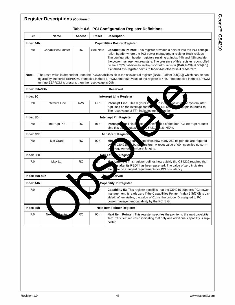
Revision 1.0 45 www.national.com
Geo
de™
CS
4210Register Descriptions (Continued)
Index 34h Capabilities Pointer Register
7:0 Capabilities Pointer RO See Note Capabilities Pointer: This register provides a pointer into the PCI configu-ration header where the PCI power management register block resides.The configuration header registers residing at Index 44h and 48h providethe power management registers. The presence of this register is controlledby the PCICapabilities bit in the nscControl register (BAR1+Offset 00h[20]).If enabled this register points to Index 44h otherwise it reads zero.
Note: The reset value is dependent upon the PCICapabilities bit in the nscControl register (BAR1+Offset 00h[20]) which can be con-figured by the serial EEPROM. If enabled in the EEPROM, the reset value of the register is 44h. If not enabled in the EEPROMor if no EEPROM is present, then the reset value is 00h.
Index 35h-3Bh Reserved
Index 3Ch Interrupt Line Register
7:0 Interrupt Line R/W FFh Interrupt Line: This register is used to identify which of the system inter-rupt lines on the interrupt controller the CS4210 interrupt pin is routed to.The reset value of FFh indicates no connection.
Index 3Dh Interrupt Pin Register
7:0 Interrupt Pin RO 01h Interrupt Pin: This register defines which of the four PCI interrupt requestpins this device uses. The CS4210 uses INTA#.
Index 3Eh Min Grant Register
7:0 Min Grant RO 00h Min Grant: This register specifies how many 250 ns periods are requiredby the CS4210 for burst transfers. A reset value of 00h specifies no strin-gent requirements on burst lengths.
Index 3Fh Max Latency Register
7:0 Max Lat RO 00h Max Latency: This register defines how quickly the CS4210 requires thePCI bus after its REQ# has been asserted. The value of zero indicatesthere are no stringent requirements for PCI bus latency.
Index 40h-43h Reserved
Index 44h Capability ID Register
7:0 CapabilityID RO 01h Capability ID: This register specifies that the CS4210 supports PCI powermanagement. It reads zero if the Capabilities Pointer (Index 34h[7:0]) is dis-abled. When visible, the value of 01h is the unique ID assigned to PCIpower management capability by the PCI SIG.
Index 45h Next Item Pointer Register
7:0 NextItemPointer RO 00h Next Item Pointer: This register specifies the pointer to the next capabilityitem. This field returns 0 indicating that only one additional capability is sup-ported.
Table 4-6. PCI Configuration Register Definitions
Bit Name Access Reset Description
Obsole
te

www.national.com 46 Revision 1.0
Geo
de™
CS
4210 Register Descriptions (Continued)
Index 46h-47h Power Management Capabilities Register
This register specifies capabilities related to PCI power management. This register is available only if the PCICapabilities bit (BAR1 Off-set 00h[20]) is set in the nscControl register.
15:11 pmeSupport RO 01000 Power Management Event Support: Bit 14 is one indicating PME# maybe asserted from the D3HOT power state. PME# is not capable of assertingfrom other states.
10 d2Support RO 0 D2 Power State Support: This bit reads zero indicating that the D2 powerstate is not supported.
9 d1Support RO 0 D1 Power State Support: This bit reads zero indicating that the D1 powerstate is not supported.
8 dynData RO 0 Dynamic Power Consumption Data: This bit reads zero indicating thatdynamic power consumption data is not provided.
7:6 RSVD RO 0 Reserved
5 DSI RO 0 Driver Special Initialization: This bit reads zero indicating that no specialinitialization is required beyond the standard PCI configuration headerbefore a generic class driver is able to use the CS4210.
4 auxPower RO 0 Auxiliary Power: This bit reads zero indicating that PME# generation in theD3COLD state is not supported.
3 pmeCLK RO 0 Power Management Event Clock: This bit reads zero indicating that nohost bus clock is required to generate PME#.
2:0 pmVerson RO 000 Power Management Version: This field reads zero indicating compatibilitywith the PCI Bus Power Interface Management Specification previous torevision 1.0.
Note: The reset value is dependent upon the PCICapabilities bit in the nscControl register (BAR1+Offset 00h[20]) which can be con-figured by serial EEPROM. If enabled in the EEPROM the reset value of this register is 4000h. If not or if no EEPROM ispresent, then the reset value is 000h.
Index 48h Power Management and Control Status Register
This register implements the control and status of the PCI power management function. This register is available only if the PCICapabil-ities bit (BAR1 Offset 00h[20]) is set in the nscControl register.
15 pmeStatus RC 1 Power Management Event Status: This bit is set when PME# is asserted.
Write 1 to clear. The PME# signal is also cleared when this is bit is writtento 1. A write of zero has no effect.
14:9 dynData RO 000000 Dynamic Power Consumption Data: This field reads 0 indicating thatdynamic data is not reported.
8 pmeEnab R/W 0 Power Management Event Enable: When set, this bit enables the asser-tion of PME#.
7:5 RSVD --- 000 Reserved
4 dynDataEnab RO Dynamic Power Consumption Data: This bit reads 0 indicating thatdynamic data is not reported.
3:2 RSVD --- 00 Reserved
1:0 pwrState R/W Power State: This field is used to determine and set the CS4210 powerstate.
00 = Current power state is D001 = Current power state is D110 = Current power state is D211 = Current power state is D3hot
Since D1 and D2 are not supported, a write of either 01 or 10 is treated asthe D0 state.
Note: The reset value is dependent upon the PCICapabilities bit in the nscControl register (BAR1+Offset 00h[20]) which can be con-figured by serial EEPROM. If enabled in the EEPROM the reset value of this register is 8000h. If not or if no EEPROM ispresent then the reset value is 000h.
Table 4-6. PCI Configuration Register Definitions
Bit Name Access Reset Description
Obsole
te

Revision 1.0 47 www.national.com
Geo
de™
CS
4210Register Descriptions (Continued)
Index 4Ah Power Management CSR Bridge Support Extension Register
7:0 pmcrBSE RO 00h Power Management Control and Status Register Bridge SupportExtension: This field returns 0 indicating that the CS4210 does not supportPCI-to-PCI bridging.
Index 4Bh Power Management Data Register
7:0 pmData RO 00h Power Management Dynamic Power Data: This field returns 0 indicatingthat the CS4210 does not report dynamic data.
Table 4-6. PCI Configuration Register Definitions
Bit Name Access Reset Description
Obsole
te
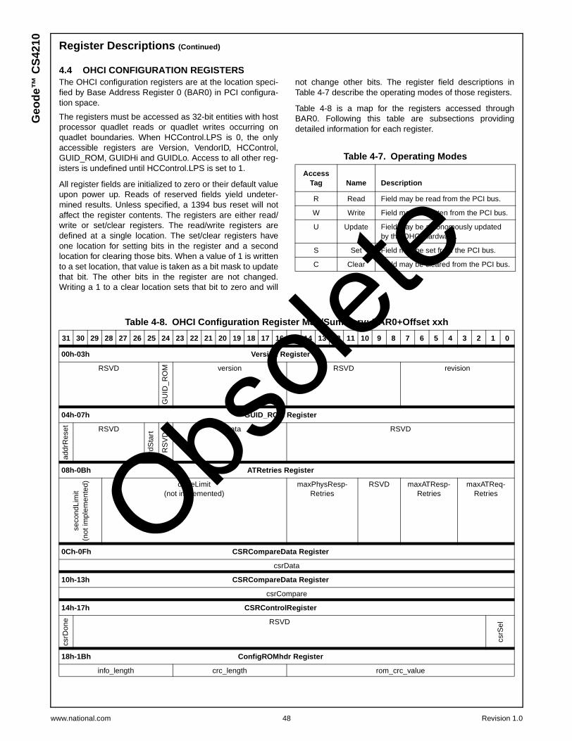
www.national.com 48 Revision 1.0
Geo
de™
CS
4210 Register Descriptions (Continued)
4.4 OHCI CONFIGURATION REGISTERSThe OHCI configuration registers are at the location speci-fied by Base Address Register 0 (BAR0) in PCI configura-tion space.
The registers must be accessed as 32-bit entities with hostprocessor quadlet reads or quadlet writes occurring onquadlet boundaries. When HCControl.LPS is 0, the onlyaccessible registers are Version, VendorID, HCControl,GUID_ROM, GUIDHi and GUIDLo. Access to all other reg-isters is undefined until HCControl.LPS is set to 1.
All register fields are initialized to zero or their default valueupon power up. Reads of reserved fields yield undeter-mined results. Unless specified, a 1394 bus reset will notaffect the register contents. The registers are either read/write or set/clear registers. The read/write registers aredefined at a single location. The set/clear registers haveone location for setting bits in the register and a secondlocation for clearing those bits. When a value of 1 is writtento a set location, that value is taken as a bit mask to updatethat bit. The other bits in the register are not changed.Writing a 1 to a clear location sets that bit to zero and will
not change other bits. The register field descriptions inTable 4-7 describe the operating modes of those registers.
Table 4-8 is a map for the registers accessed throughBAR0. Following this table are subsections providingdetailed information for each register.
Table 4-7. Operating Modes
AccessTag Name Description
R Read Field may be read from the PCI bus.
W Write Field may be written from the PCI bus.
U Update Field may be autonomously updatedby the OHCI hardware.
S Set Field may be set from the PCI bus.
C Clear Field may be cleared from the PCI bus.
Table 4-8. OHCI Configuration Register Map/Summary: BAR0+Offset xxh
31 30 29 28 27 26 25 24 23 22 21 20 19 18 17 16 15 14 13 12 11 10 9 8 7 6 5 4 3 2 1 0
00h-03h Version Register
RSVD
GU
ID_R
OM version RSVD revision
04h-07h GUID_ROM Register
addr
Res
et RSVD
rdS
tart
RS
VD
rdData RSVD
08h-0Bh ATRetries Register
seco
ndLi
mit
(not
impl
emen
ted) cycleLimit
(not implemented)maxPhysResp-
RetriesRSVD maxATResp-
RetriesmaxATReq-
Retries
0Ch-0Fh CSRCompareData Register
csrData
10h-13h CSRCompareData Register
csrCompare
14h-17h CSRControlRegister
csrD
one RSVD
csrS
el
18h-1Bh ConfigROMhdr Register
info_length crc_length rom_crc_value
Obsole
te
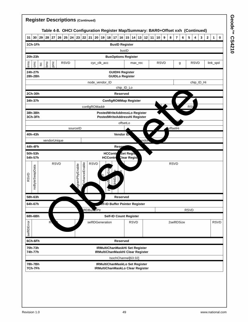
Revision 1.0 49 www.national.com
Geo
de™
CS
4210Register Descriptions (Continued)
1Ch-1Fh BusID Register
busID
20h-23h BusOptions Register
irms
cmc
isc
bmc
pmc RSVD cyc_clk_acc max_rec RSVD g RSVD link_spd
24h-27h GUIDHi Register28h-2Bh GUIDLo Register
node_vendor_ID chip_ID_Hi
chip_ID_Lo
2Ch-30h Reserved
34h-37h ConfigROMMap Register
configROMaddr RSVD
38h-3Bh PostedWriteAddressLo Register3Ch-3Fh PostedWriteAddressHi Register
offsetLo
sourceID offsetHi
40h-43h Vendor ID
vendorUnique vendorCompanyID
44h-4Fh Reserved
50h-53h HCControl Set Register54h-57h HCControl Clear Register
RS
VD
noB
yteS
wap
Dat
a RSVD
prog
ram
Phy
Ena
ble
aPhy
Enh
ance
Ena
ble RSVD
LPS
post
edW
riteE
nabl
e
linkE
nabl
e
softR
eset
RSVD
58h-63h Reserved
64h-67h Self-ID Buffer Pointer Register
selfIDBufferPtr RSVD
68h-6Bh Self-ID Count Register
selfI
DE
rror RSVD selfIDGeneration RSVD 2selfIDSize RSVD
6Ch-6Fh Reserved
70h-73h IRMultiChanMaskHi Set Register74h-77h IRMultiChanMaskHi Clear Register
IsochChannel[63:32]
78h-7Bh IRMultiChanMaskLo Set Register7Ch-7Fh IRMultiChanMaskLo Clear Register
Table 4-8. OHCI Configuration Register Map/Summary: BAR0+Offset xxh (Continued)
31 30 29 28 27 26 25 24 23 22 21 20 19 18 17 16 15 14 13 12 11 10 9 8 7 6 5 4 3 2 1 0
Obsole
te
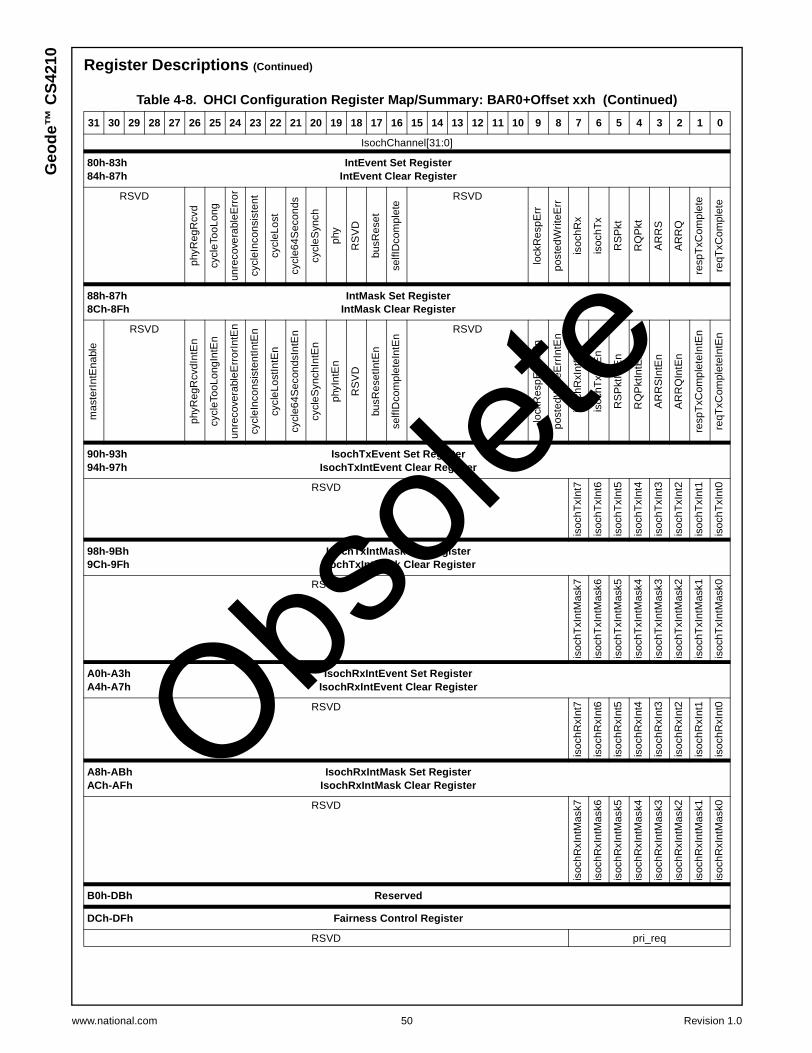
www.national.com 50 Revision 1.0
Geo
de™
CS
4210 Register Descriptions (Continued)
IsochChannel[31:0]
80h-83h IntEvent Set Register84h-87h IntEvent Clear Register
RSVDph
yReg
Rcv
d
cycl
eToo
Long
unre
cove
rabl
eErr
or
cycl
eInc
onsi
sten
t
cycl
eLos
t
cycl
e64S
econ
ds
cycl
eSyn
ch
phy
RS
VD
busR
eset
selfI
Dco
mpl
ete
RSVD
lock
Res
pErr
post
edW
riteE
rr
isoc
hRx
isoc
hTx
RS
Pkt
RQ
Pkt
AR
RS
AR
RQ
resp
TxC
ompl
ete
reqT
xCom
plet
e
88h-87h IntMask Set Register8Ch-8Fh IntMask Clear Register
mas
terI
ntE
nabl
e
RSVD
phyR
egR
cvdI
ntE
n
cycl
eToo
Long
IntE
n
unre
cove
rabl
eErr
orIn
tEn
cycl
eInc
onsi
sten
tIntE
n
cycl
eLos
tIntE
n
cycl
e64S
econ
dsIn
tEn
cycl
eSyn
chIn
tEn
phyI
ntE
n
RS
VD
busR
eset
IntE
n
selfI
Dco
mpl
eteI
ntE
n
RSVD
lock
Res
pErr
IntE
n
post
edW
riteE
rrIn
tEn
isoc
hRxI
ntE
n
isoc
hTxI
ntE
n
RS
Pkt
IntE
n
RQ
Pkt
IntE
n
AR
RS
IntE
n
AR
RQ
IntE
n
resp
TxC
ompl
eteI
ntE
n
reqT
xCom
plet
eInt
En
90h-93h IsochTxEvent Set Register94h-97h IsochTxIntEvent Clear Register
RSVD
isoc
hTxI
nt7
isoc
hTxI
nt6
isoc
hTxI
nt5
isoc
hTxI
nt4
isoc
hTxI
nt3
isoc
hTxI
nt2
isoc
hTxI
nt1
isoc
hTxI
nt0
98h-9Bh IsochTxIntMask Set Register9Ch-9Fh IsochTxIntMask Clear Register
RSVDis
ochT
xInt
Mas
k7
isoc
hTxI
ntM
ask6
isoc
hTxI
ntM
ask5
isoc
hTxI
ntM
ask4
isoc
hTxI
ntM
ask3
isoc
hTxI
ntM
ask2
isoc
hTxI
ntM
ask1
isoc
hTxI
ntM
ask0
A0h-A3h IsochRxIntEvent Set RegisterA4h-A7h IsochRxIntEvent Clear Register
RSVD
isoc
hRxI
nt7
isoc
hRxI
nt6
isoc
hRxI
nt5
isoc
hRxI
nt4
isoc
hRxI
nt3
isoc
hRxI
nt2
isoc
hRxI
nt1
isoc
hRxI
nt0
A8h-ABh IsochRxIntMask Set RegisterACh-AFh IsochRxIntMask Clear Register
RSVD
isoc
hRxI
ntM
ask7
isoc
hRxI
ntM
ask6
isoc
hRxI
ntM
ask5
isoc
hRxI
ntM
ask4
isoc
hRxI
ntM
ask3
isoc
hRxI
ntM
ask2
isoc
hRxI
ntM
ask1
isoc
hRxI
ntM
ask0
B0h-DBh Reserved
DCh-DFh Fairness Control Register
RSVD pri_req
Table 4-8. OHCI Configuration Register Map/Summary: BAR0+Offset xxh (Continued)
31 30 29 28 27 26 25 24 23 22 21 20 19 18 17 16 15 14 13 12 11 10 9 8 7 6 5 4 3 2 1 0
Obsole
te

Revision 1.0 51 www.national.com
Geo
de™
CS
4210Register Descriptions (Continued)
E0h-E3h LinkControl Set RegisterE4h-E7h LinkControl Clear Register
RSVD
cycl
eSou
rce
cycl
eMas
ter
cycl
eTim
erE
nabl
e RSVD
rcvP
hyP
kt
rcvS
elfID
RSVD
E8h-EBh Node ID and Status Register
iDV
alid
root
RSVD
CP
S RSVD busNumber nodeNumber
ECh-EFh PHYControl Register
rdD
one RSVD rdAddr rdData
rdR
eg
wrR
eg RSVD regAddr wrData
F0h-F3h IsochCycleTimer Register
cycleSeconds cycleCount cycleOffset
F4h-FFh Reserved
100h-103h AsyncReqFilterHi Set Register104h-107h AsyncReqFilterHi Clear Register
asyn
cReq
Res
ourc
eAll asyncReqResource[62:32]
108h-10Bh AsyncReqFilterLo Set Register10Ch-10Fh AsyncReqFilterLo Clear Register
asyncReqResource[31:0]
110h-113h PhysicalReqHi Set Register114h-117h PhysicalReqHi Clear Register
phys
Req
Res
ourc
eAll physReqResource[62:32]
118h-11Bh PhysicalReqtLo Set Register11Ch-11Fh PhysicalRequestLo Clear Register
physReqResource[31:0]
120h-17Fh Reserved
Table 4-8. OHCI Configuration Register Map/Summary: BAR0+Offset xxh (Continued)
31 30 29 28 27 26 25 24 23 22 21 20 19 18 17 16 15 14 13 12 11 10 9 8 7 6 5 4 3 2 1 0
Obsole
te

www.national.com 52 Revision 1.0
Geo
de™
CS
4210 Register Descriptions (Continued)
180h-183h AsyncReqTxContextControl Set Register184h-187h AsyncReqTxContextControl Clear Register
RSVD
run FSVD
wak
e
dead
activ
e RSVD event code
188h-18Bh Reserved
18Ch-18Fh AsyncReqTxCommandPtr Register
descriptorAddress Z
190h-19Fh Reserved
1A0h-1A3h AsyncRespTxContextControl Set Register1A4h-1A7h AsyncRespTxContextControl Clear Register
RSVD
run RSVD
wak
e
dead
activ
e RSVD event code
1A8h-1ABh Reserved
1ACh-1AFh AsyncRespTxCommandPtr Register
descriptoraddress Z
1B0h-1BFh Reserved
1C0h-1C3h AsyncReqRxContextControl Set Register1C4h-1C7h AsyncReqRxContextControl Clear Register
RSVD
run RSVD
wak
e
dead
activ
e RSVD spd event code
1C8h-1CBh Reserved
1CCh-1CFh AsyncReqRxCommandPtr Register
descriptorAddress Z
1D0h-1DFh Reserved
1E0h-1E3h AsyncRespRxContextControl Set Register1E4h-1E7h AsyncRespRxContextControl Clear Register
RSVD
run RSVD
wak
e
dead
activ
e RSVD spd event code
1E8h-1EBh Reserved
1ECh-1EFh AsyncRespRxCommandPtr Register
descriptorAddress Z
1F0h-1FFh Reserved
200h-203h IsochTx0ContextControl Set Register204h-207h IsochTx0ContextControl Clear Register
cycl
eMat
chE
nabl
e cyclematch
run
RSVD
wak
e
dead
activ
e
RSVD event code
208h-20Bh Reserved
20Ch-20Fh IsochTx0CommandPtr Register
descriptorAddress Z
Table 4-8. OHCI Configuration Register Map/Summary: BAR0+Offset xxh (Continued)
31 30 29 28 27 26 25 24 23 22 21 20 19 18 17 16 15 14 13 12 11 10 9 8 7 6 5 4 3 2 1 0
Obsole
te

Revision 1.0 53 www.national.com
Geo
de™
CS
4210Register Descriptions (Continued)
210h-213h IsochTx1ContextControl Set Register214h-217h IsochTx1ContextControl Clear Register
cycl
eMat
chE
nabl
e cyclematch
run
RSVD
wak
e
dead
activ
e
RSVD event code
218h-21Bh Reserved
21Ch-21Fh IsochTx1CommandPtr Register
descriptorAddress Z
220h-223h IsochTx2ContextControl Set Register224h-227h IsochTx2ContextControl Clear Register
cycl
eMat
chE
nabl
e cyclematch
run
RSVD
wak
e
dead
activ
e
RSVD event code
228h-22Bh Reserved
22Ch-22Fh IsochTx2CommandPtr Register
descriptorAddress Z
230h-233h IsochTx3ContextControl Set Register234h-237h IsochTx3ContextControl Clear Register
cycl
eMat
chE
nabl
e cyclematch
run
RSVD
wak
e
dead
activ
e
RSVD event code
238h-23Bh Reserved
23Ch-23Fh IsochTx3CommandPtr Register
descriptorAddress Z
240h-243h IsochTx4ContextControl Set Register244h-247h IsochTx4ContextControl Clear Register
cycl
eMat
chE
nabl
e cyclematch
run
RSVD
wak
e
dead
activ
e
RSVD event code
248h-24Bh Reserved
24Ch-24Fh IsochTx4CommandPtr Register
descriptorAddress Z
Table 4-8. OHCI Configuration Register Map/Summary: BAR0+Offset xxh (Continued)
31 30 29 28 27 26 25 24 23 22 21 20 19 18 17 16 15 14 13 12 11 10 9 8 7 6 5 4 3 2 1 0
Obsole
te
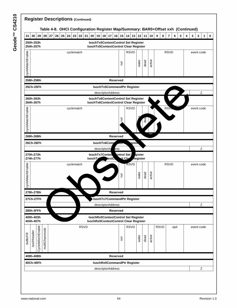
www.national.com 54 Revision 1.0
Geo
de™
CS
4210 Register Descriptions (Continued)
250h-253h IsochTx5ContextControl Set Register254h-257h IsochTx5ContextControl Clear Register
cycl
eMat
chE
nabl
e cyclematch
run
RSVD
wak
e
dead
activ
e
RSVD event code
258h-25Bh Reserved
25Ch-25Fh IsochTx5CommandPtr Register
descriptorAddress Z
260h-263h IsochTx6ContextControl Set Register264h-267h IsochTx6ContextControl Clear Register
cycl
eMat
chE
nabl
e cyclematch
run
RSVD
wak
e
dead
activ
e
RSVD event code
268h-26Bh Reserved
26Ch-26Fh IsochTx6CommandPtr Register
descriptorAddress Z
270h-273h IsochTx7ContextControl Set Register274h-277h IsochTx7ContextControl Clear Register
cycl
eMat
chE
nabl
e cyclematch
run
RSVD
wak
e
dead
activ
e
RSVD event code
278h-27Bh Reserved
27Ch-27Fh IsochTx7CommandPtr Register
descriptorAddress Z
280h-3FFh Reserved
400h-403h IsochRx0ContextControl Set Register404h-407h IsochRx0ContextControl Clear Register
buffe
rFill
isoc
hhea
der
Cyc
leM
Atc
hEna
ble
mul
tiCha
nmod
e RSVD
run
RSVD
wak
e
dead
activ
e
RSVD spd event code
408h-40Bh Reserved
40Ch-40Fh IsochRx0CommandPtr Register
descriptorAddress Z
Table 4-8. OHCI Configuration Register Map/Summary: BAR0+Offset xxh (Continued)
31 30 29 28 27 26 25 24 23 22 21 20 19 18 17 16 15 14 13 12 11 10 9 8 7 6 5 4 3 2 1 0
Obsole
te
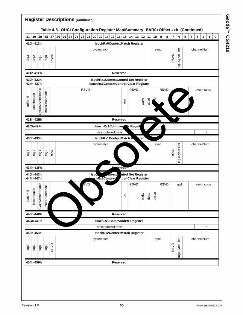
Revision 1.0 55 www.national.com
Geo
de™
CS
4210Register Descriptions (Continued)
410h-413h IsochRx0ContextMatch Register
tag3
tag2
tag1
tag0
RS
VD
cyclematch sync
RS
VD
tag1
Syn
cFilt
er channelNum
414h-41Fh Reserved
420h-423h IsochRx1ContextControl Set Register424h-427h IsochRx1ContextControl Clear Register
buffe
rFill
isoc
hhea
der
Cyc
leM
Atc
hEna
ble
mul
tiCha
nmod
e RSVD
run
RSVD
wak
e
dead
activ
e
RSVD spd event code
428h-42Bh Reserved
42Ch-42Fh IsochRx1CommandPtr Register
descriptorAddress Z
430h-433h IsochRx1ContextMatch Register
tag3
tag2
tag1
tag0
RS
VD
cyclematch sync
RS
VD
tag1
Syn
cFilt
er channelNum
434h-43Fh Reserved
440h-443h IsochRx2ContextControl Set Register444h-447h IsochRx2ContextControl Clear Register
buffe
rFill
isoc
hhea
der
Cyc
leM
Atc
hEna
ble
mul
tiCha
nmod
e RSVD
run
RSVD
wak
e
dead
activ
e
RSVD spd event code
448h-44Bh Reserved
44Ch-44Fh IsochRx2CommandPtr Register
descriptorAddress Z
450h-453h IsochRx2ContextMatch Register
tag3
tag2
tag1
tag0
RS
VD
cyclematch sync
RS
VD
tag1
Syn
cFilt
er channelNum
454h-45Fh Reserved
Table 4-8. OHCI Configuration Register Map/Summary: BAR0+Offset xxh (Continued)
31 30 29 28 27 26 25 24 23 22 21 20 19 18 17 16 15 14 13 12 11 10 9 8 7 6 5 4 3 2 1 0
Obsole
te

www.national.com 56 Revision 1.0
Geo
de™
CS
4210 Register Descriptions (Continued)
460h-463h IsochRx3ContextControl Set Register464h-467h IsochRx3ContextControl Clear Register
buffe
rFill
isoc
hhea
der
Cyc
leM
Atc
hEna
ble
mul
tiCha
nmod
e RSVD
run
RSVD
wak
e
dead
activ
e
RSVD spd event code
468h-46Bh Reserved
46Ch-46Fh IsochRx3CommandPtr Register
descriptorAddress Z
470h-473h IsochRx3ContextMatch Register
tag3
tag2
tag1
tag0
RS
VD
cyclematch sync
RS
VD
tag1
Syn
cFilt
er channelNum
474h-47Fh Reserved
480h-483h IsochRx4ContextControl Set Register484h-487h IsochRx4ContextControl Clear Register
buffe
rFill
isoc
hhea
der
Cyc
leM
Atc
hEna
ble
mul
tiCha
nmod
e RSVD
run
RSVD
wak
e
dead
activ
e
RSVD spd event code
488h-48Bh Reserved
48Ch-48Fh IsochRx4CommandPtr Register
descriptorAddress Z
490h-493h IsochRx4ContextMatch Register
tag3
tag2
tag1
tag0
RS
VD
cyclematch sync
RS
VD
tag1
Syn
cFilt
er channelNum
494h-49Fh Reserved
4A0h-4A3h IsochRx5ContextControl Set Register4A4h-4A7h IsochRx5ContextControl Clear Register
buffe
rFill
isoc
hhea
der
Cyc
leM
Atc
hEna
ble
mul
tiCha
nmod
e RSVD
run
RSVD
wak
e
dead
activ
e
RSVD spd event code
4A8h-4ABh Reserved
4ACh-4AFh IsochRx5CommandPtr Register
descriptorAddress Z
Table 4-8. OHCI Configuration Register Map/Summary: BAR0+Offset xxh (Continued)
31 30 29 28 27 26 25 24 23 22 21 20 19 18 17 16 15 14 13 12 11 10 9 8 7 6 5 4 3 2 1 0
Obsole
te
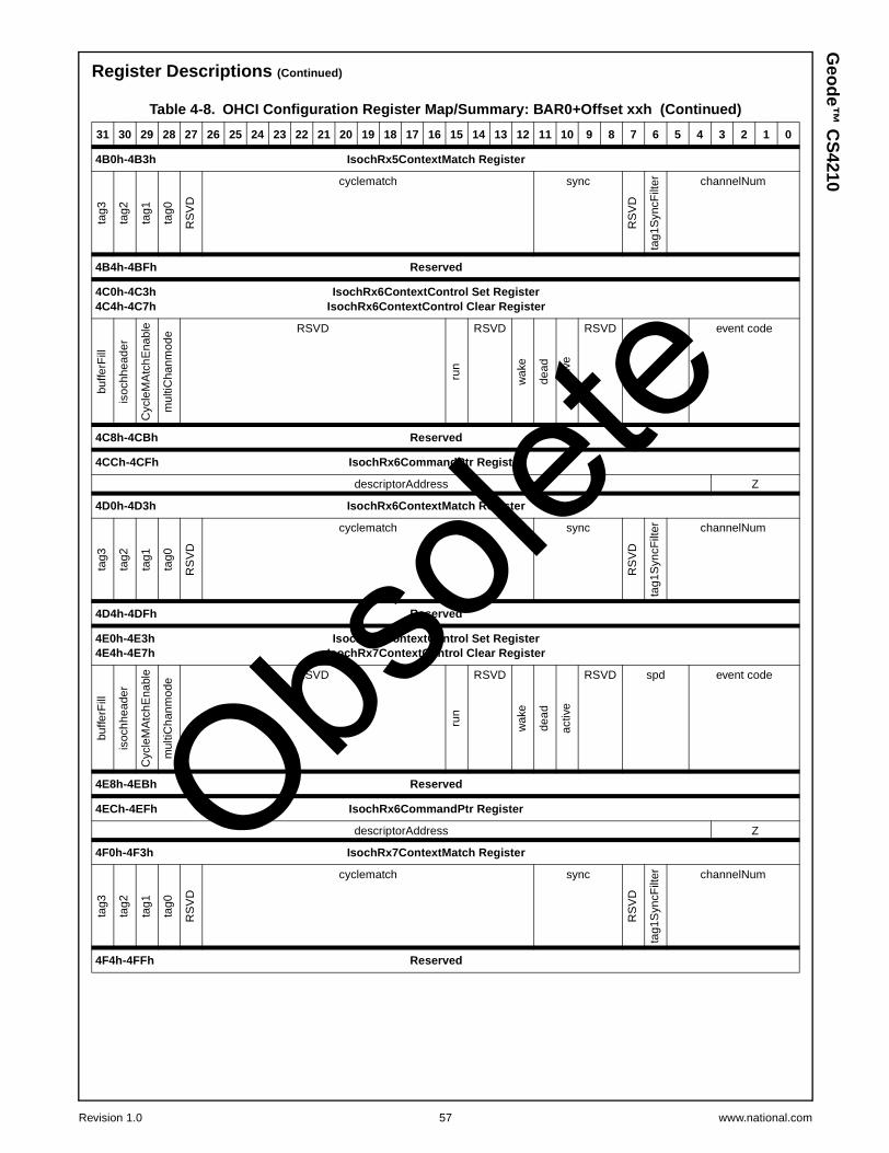
Revision 1.0 57 www.national.com
Geo
de™
CS
4210Register Descriptions (Continued)
4B0h-4B3h IsochRx5ContextMatch Register
tag3
tag2
tag1
tag0
RS
VD
cyclematch sync
RS
VD
tag1
Syn
cFilt
er channelNum
4B4h-4BFh Reserved
4C0h-4C3h IsochRx6ContextControl Set Register4C4h-4C7h IsochRx6ContextControl Clear Register
buffe
rFill
isoc
hhea
der
Cyc
leM
Atc
hEna
ble
mul
tiCha
nmod
e RSVD
run
RSVD
wak
e
dead
activ
e
RSVD spd event code
4C8h-4CBh Reserved
4CCh-4CFh IsochRx6CommandPtr Register
descriptorAddress Z
4D0h-4D3h IsochRx6ContextMatch Register
tag3
tag2
tag1
tag0
RS
VD
cyclematch sync
RS
VD
tag1
Syn
cFilt
er channelNum
4D4h-4DFh Reserved
4E0h-4E3h IsochRx7ContextControl Set Register4E4h-4E7h IsochRx7ContextControl Clear Register
buffe
rFill
isoc
hhea
der
Cyc
leM
Atc
hEna
ble
mul
tiCha
nmod
e RSVD
run
RSVD
wak
e
dead
activ
e
RSVD spd event code
4E8h-4EBh Reserved
4ECh-4EFh IsochRx6CommandPtr Register
descriptorAddress Z
4F0h-4F3h IsochRx7ContextMatch Register
tag3
tag2
tag1
tag0
RS
VD
cyclematch sync
RS
VD
tag1
Syn
cFilt
er channelNum
4F4h-4FFh Reserved
Table 4-8. OHCI Configuration Register Map/Summary: BAR0+Offset xxh (Continued)
31 30 29 28 27 26 25 24 23 22 21 20 19 18 17 16 15 14 13 12 11 10 9 8 7 6 5 4 3 2 1 0
Obsole
te

www.national.com 58 Revision 1.0
Geo
de™
CS
4210 Register Descriptions (Continued)
4.4.1 Version RegisterThe Version register (Table 4-9) contains a 32-bit valuewhich indicates the version and capabilities of the interface.The register is expected to be used to indicate the level offunctionality present in the CS4210.
4.4.2 GUIDROM RegisterThe Global Unique ID ROM register (Table 4-10) is used toaccess the GUID ROM. To initialize the GUID ROM read
address, software sets GUIDROM.addrReset to one. Oncesoftware detects that GUIDROM.addrReset is zero, indicat-ing that the reset has completed, then software may setGUIDROM.rdStart to read a byte. Upon the completion ofeach read, the CS4210 places the read byte intoGUIDROM.rdData, advances the GUID ROM address byone byte to set up for the next read, and clearsGUIDROM.rdStart to 0 to indicate to software that therequested byte has been read.
Table 4-9. BAR0+Offset 00h: Version Register
Bit Name Access Reset Description
31:25 RSVD -- 0 Reserved
24 GUID_ROM R N/A Global Unique ID ROM: The third and fourth quadlets of theBus_Info_Block are automatically loaded on hardware reset.
23:16 version R 01h Major Version: This field contains the BCD encoded value representing themajor version of the highest numbered 1394 OpenHCI specification withwhich the CS4210 is compliant.
15:8 RSVD -- 0 Reserved
7:0 revision R 0 Minor Version: This field contains the BCD encoded value representingthe minor version of the highest numbered 1394 OpenHCI specification withwhich the CS4210 is compliant.
Table 4-10. BAR0+Offset 04h: GUID ROM Register
Bit Name Access Reset Description
31 addrReset RSU 0 Address Reset: Software sets this bit to one to reset the GUID ROMaddress to zero. When the CS4210 completes the reset, it clears addrResetto zero. Upon resetting the GUID ROM address, the CS4210 does not auto-matically fill rdData with the data from byte address 0.
30:26 RSVD -- 0 Reserved
25 rdStart RSU 0 Read Start: A read of the currently addressed GUID ROM byte is startedon the transition of this bit from a zero to a one. When the CS4210 com-pletes the read, it clears rdStart to zero and advances the GUID ROM byteaddress by one byte.
24 RSVD -- 0 Reserved
23:16 rdData RU Undef Read Data: The data read from the GUID ROM.
15:0 RSVD -- 0 ReservedObsole
te

Revision 1.0 59 www.national.com
Geo
de™
CS
4210Register Descriptions (Continued)
4.4.3 ATRetries RegisterThe ATRetries register (Table 4-11) holds the number oftimes the CS4210 attempts to do a retry for asynchronousDMA request transmit and for asynchronous physical andDMA response transmit. A packet may only be retried when
a “busy” acknowledge or ack_data_error is received fromthe target node, including ack_data_error’s resulting fromFIFO underflows. A packet is not retried under any othercircumstance, including receipt of evt_missing_ack.
Table 4-11. BAR0+Offset 08h: ATRetries Register
Bit Name Access Reset Description
31:29 secondLimit R 0 Second Limit: Not implemented.
28:16 cycleLimit R 0 Cycle Limit: Not implemented.
15:11 maxPhysRespRe-tries
RW Undef Maximum Physical Response Retries: This field tells the response unitwithin the RDMA module how many times to attempt to retry the transmitoperation for the response packet. Note that this value is used only forresponses to physical requests.
If the retry count expires for a physical response, the packet is discarded bythe CS4210. Software is not notified.
10:8 RSVD -- 0 Reserved
7:4 maxATRespRetries RW Undef Maximum AT Physical Response Retries: This field tells the asynchro-nous transmit response unit within the ATDMA module how many times toattempt to retry the transmit operation for a software transmitted (non-phys-ical) asynchronous response packet.
3:0 maxATReqRetries RW Undef Maximum AT Request Retries: This field tells the asynchronous transmitrequest unit within the ATDMA how many times to attempt to retry the trans-mit operation for an asynchronous request packet.
Obsole
te

www.national.com 60 Revision 1.0
Geo
de™
CS
4210 Register Descriptions (Continued)
4.4.4 Autonomous CSR ResourcesThe CS4210 implements a number of autonomous CSRresources. In particular the 1394 compare-swap bus man-agement registers are implemented in hardware, as is theconfig ROM header, the Bus_Info_Block and access to thefirst 1 KB of the configuration ROM. The DMA units handleexternal 1394 bus requests to these resources automati-cally. The serial bus registers shown in Table 4-12 managethis function for the local host. 1394 requires certain 1394bus management resource registers be accessible only via“quadlet read” and “quadlet lock” (compare-and-swap)transactions, otherwise ack_type_error is sent. These spe-cial bus management resource registers are implementedinternal to the CS4210 to allow atomic compare-and-swapaccess from either the host system or from the 1394 bus.
When these serial bus management resource registers areaccessed from the 1394 bus, the atomic compare-and-swap transaction is autonomous, without software interven-tion. If ack_complete is not received to end the transaction
for the generated lock response, IntEvent.lockRespErr(refer to Table 4-26 on page 70) is triggered. To accessthese bus management resource registers from the host,the registers shown in Table 4-13 are used. To accessthese bus management resource registers from the hostbus, first load the CSRReadData register with the new datavalue to be loaded into the appropriate resource. Then loadthe CSRCompareData register with the expected value.Finally, write the CSRControl register with the selectorvalue of the resource. A write to the CSRControl registerinitiates a compare-and-swap operation on the selectedresource. When the compare-and-swap operation is com-plete, the CSRControl register csrDone bit is set, and theCSRReadData register contains the value of the selectedresource prior to the host initiated compare-and-swapoperation. Note that an arbitrary update of these resourcescannot be done. Only compare-and-swap operations canbe used to modify the contents of these internal resourceregisters.
Table 4-12. Serial Bus Registers
CSR AddresscsrSel Bits
(BAR0+Offset 14h[1:0] Description1394-1995Section #
Reset (Hardware orBus Reset)
FFFF_F000_021Ch 00 BUS_MANAGER_ID 8.3.2.3.6 03Fh
FFFF_F000_0220h 01 BANDWIDTH_AVAILABLE 8.3.2.3.7 1333h
FFFF_F000_0224h 10 CHANNELS_AVAILABLE_HI 8.3.2.3.8 FFFF_FFFFh
FFFF_F000_0228h 11 CHANNELS_AVAILABLE_LO 8.3.2.3.8 FFFF_FFFFh
Table 4-13. CSR Registers
Bit Name Access Reset Description
BAR0+Offset 0Ch CSRReadData Register
31:0 csrData RWU Undef Control/Status Register Read Data: At start of operation, the data to bestored if the compare is successful.
BAR0+Offset 10h CSRCompareData Register
31:0 csrCompare RW Undef Control/Status Register Compare: The data to be compared with theexisting value of the CSR resource.
BAR0+Offset 14h CSRControl Register
31 csrDone RU 1 Control/Status Register Done: This bit is set when a compare-swap oper-ation is completed. It is reset whenever this register is written.
30:2 RSVD -- 0 Reserved
1:0 csrSel RW Undef Control/Status Register Resource Selection:
00 = BUS_MANAGER_ID01 = BANDWIDTH_AVAILABLE10 = CHANNELS_AVAILABLE_HI11 = CHANNELS_AVAILABLE_LO
Obsole
te

Revision 1.0 61 www.national.com
Geo
de™
CS
4210Register Descriptions (Continued)
4.4.5 Configuration ROM Header RegisterThe configuration ROM header register (Table 4-14) is a32-bit number that externally maps to the 1st quadlet of the1394 configuration ROM (1394 address at offsetFFFF_F000_0400h). This register is written locally atBAR0+Offset 18h.
4.4.6 Bus Identification RegisterThe Bus Identification register (Table 4-15) is a 32-bit num-ber that externally maps to the first quadlet of theBus_Info_Block.
Table 4-14. BAR0+Offset 18h: ConfigROMhdr Register
Bit Name Access Reset Description
31:24 info_length RWU 00h Information Length: IEEE 1394 bus management field. Must be valid atany time the HCControl.linkEnable bit (BAR0+Offset 50h[17]) is set.
23:!6 crc_length RWU 00h Cyclical Redundancy Check Length: IEEE 1394 bus management field.Must be valid at any time the HCControl.linkEnable bit (BAR0+Offset50h[17]) is set.
15:0 rom_crc_value RWU 0000h ROM Cyclical Redundancy Check Value: IEEE 1394 bus managementfield. Must be valid at any time the HCControl.linkEnable bit (BAR0+Offset50h[17]) is set.
Table 4-15. BAR0+Offset 1Ch: Bus Identification Register
Bit Name Access Reset Description
31:0 busID R 31333934h Bus Identification: This 32-bit number externally maps to the first quadlet ofthe Bus_Info_Block. It contains the constant 31333934h which is the ASCIIvalue for “1394”.
Obsole
te
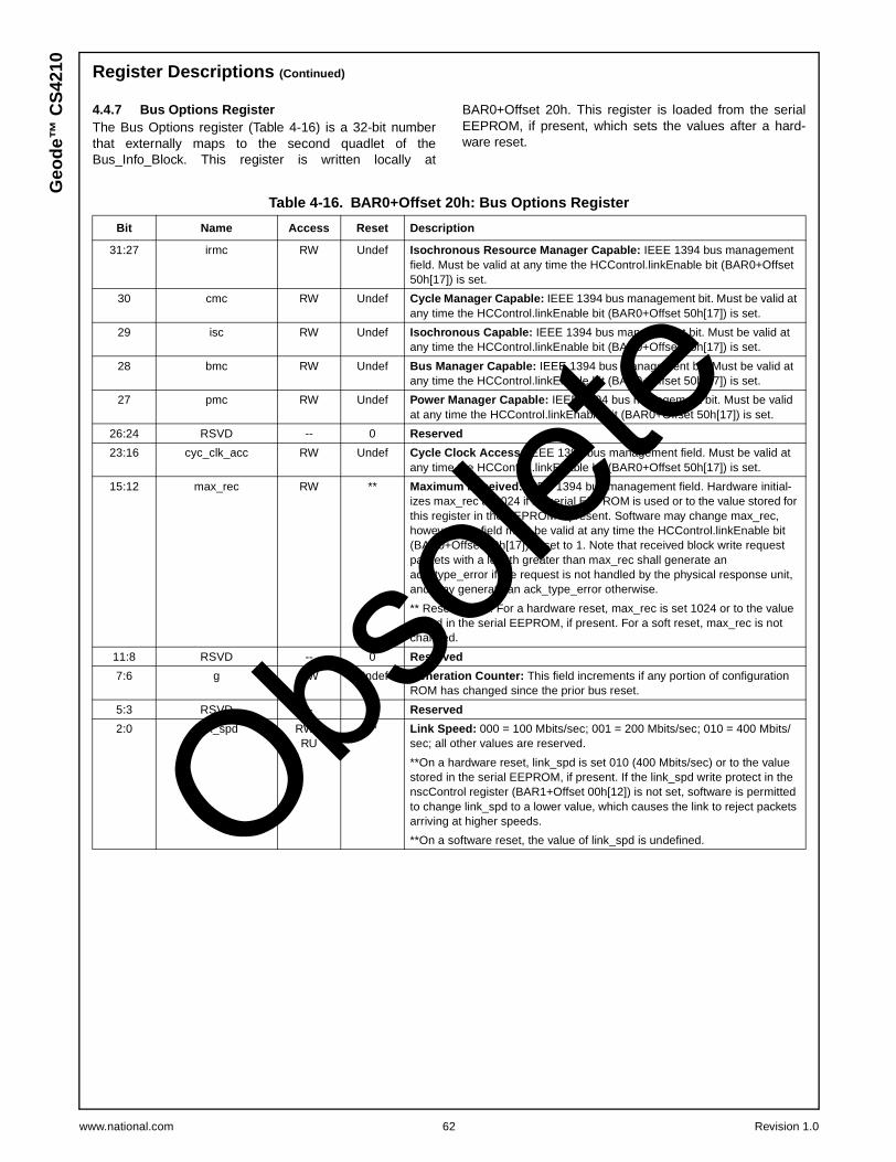
www.national.com 62 Revision 1.0
Geo
de™
CS
4210 Register Descriptions (Continued)
4.4.7 Bus Options RegisterThe Bus Options register (Table 4-16) is a 32-bit numberthat externally maps to the second quadlet of theBus_Info_Block. This register is written locally at
BAR0+Offset 20h. This register is loaded from the serialEEPROM, if present, which sets the values after a hard-ware reset.
Table 4-16. BAR0+Offset 20h: Bus Options Register
Bit Name Access Reset Description
31:27 irmc RW Undef Isochronous Resource Manager Capable: IEEE 1394 bus managementfield. Must be valid at any time the HCControl.linkEnable bit (BAR0+Offset50h[17]) is set.
30 cmc RW Undef Cycle Manager Capable: IEEE 1394 bus management bit. Must be valid atany time the HCControl.linkEnable bit (BAR0+Offset 50h[17]) is set.
29 isc RW Undef Isochronous Capable: IEEE 1394 bus management bit. Must be valid atany time the HCControl.linkEnable bit (BAR0+Offset 50h[17]) is set.
28 bmc RW Undef Bus Manager Capable: IEEE 1394 bus management bit. Must be valid atany time the HCControl.linkEnable bit (BAR0+Offset 50h[17]) is set.
27 pmc RW Undef Power Manager Capable: IEEE 1394 bus management bit. Must be validat any time the HCControl.linkEnable bit (BAR0+Offset 50h[17]) is set.
26:24 RSVD -- 0 Reserved
23:16 cyc_clk_acc RW Undef Cycle Clock Access: IEEE 1394 bus management field. Must be valid atany time the HCControl.linkEnable bit (BAR0+Offset 50h[17]) is set.
15:12 max_rec RW ** Maximum Received: IEEE 1394 bus management field. Hardware initial-izes max_rec to 1024 if no serial EEPROM is used or to the value stored forthis register in the EEPROM if present. Software may change max_rec,however, this field must be valid at any time the HCControl.linkEnable bit(BAR0+Offset 50h[17]) is set to 1. Note that received block write requestpackets with a length greater than max_rec shall generate anack_type_error if the request is not handled by the physical response unit,and may generate an ack_type_error otherwise.
** Reset values: For a hardware reset, max_rec is set 1024 or to the valuestored in the serial EEPROM, if present. For a soft reset, max_rec is notchanged.
11:8 RSVD -- 0 Reserved
7:6 g RW Undef Generation Counter: This field increments if any portion of configurationROM has changed since the prior bus reset.
5:3 RSVD -- 0 Reserved
2:0 link_spd RWURU
** Link Speed: 000 = 100 Mbits/sec; 001 = 200 Mbits/sec; 010 = 400 Mbits/sec; all other values are reserved.
**On a hardware reset, link_spd is set 010 (400 Mbits/sec) or to the valuestored in the serial EEPROM, if present. If the link_spd write protect in thenscControl register (BAR1+Offset 00h[12]) is not set, software is permittedto change link_spd to a lower value, which causes the link to reject packetsarriving at higher speeds.
**On a software reset, the value of link_spd is undefined.Obsole
te
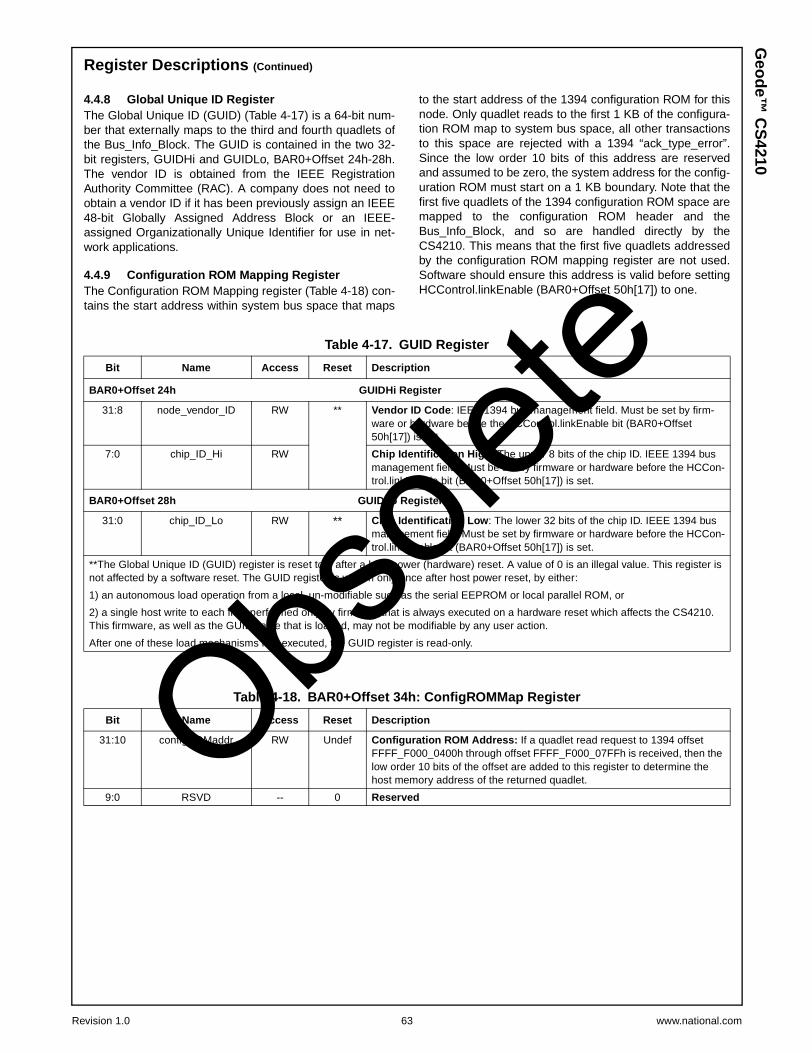
Revision 1.0 63 www.national.com
Geo
de™
CS
4210Register Descriptions (Continued)
4.4.8 Global Unique ID RegisterThe Global Unique ID (GUID) (Table 4-17) is a 64-bit num-ber that externally maps to the third and fourth quadlets ofthe Bus_Info_Block. The GUID is contained in the two 32-bit registers, GUIDHi and GUIDLo, BAR0+Offset 24h-28h.The vendor ID is obtained from the IEEE RegistrationAuthority Committee (RAC). A company does not need toobtain a vendor ID if it has been previously assign an IEEE48-bit Globally Assigned Address Block or an IEEE-assigned Organizationally Unique Identifier for use in net-work applications.
4.4.9 Configuration ROM Mapping RegisterThe Configuration ROM Mapping register (Table 4-18) con-tains the start address within system bus space that maps
to the start address of the 1394 configuration ROM for thisnode. Only quadlet reads to the first 1 KB of the configura-tion ROM map to system bus space, all other transactionsto this space are rejected with a 1394 “ack_type_error”.Since the low order 10 bits of this address are reservedand assumed to be zero, the system address for the config-uration ROM must start on a 1 KB boundary. Note that thefirst five quadlets of the 1394 configuration ROM space aremapped to the configuration ROM header and theBus_Info_Block, and so are handled directly by theCS4210. This means that the first five quadlets addressedby the configuration ROM mapping register are not used.Software should ensure this address is valid before settingHCControl.linkEnable (BAR0+Offset 50h[17]) to one.
Table 4-17. GUID Register
Bit Name Access Reset Description
BAR0+Offset 24h GUIDHi Register
31:8 node_vendor_ID RW ** Vendor ID Code: IEEE 1394 bus management field. Must be set by firm-ware or hardware before the HCControl.linkEnable bit (BAR0+Offset50h[17]) is set.
7:0 chip_ID_Hi RW Chip Identification High: The upper 8 bits of the chip ID. IEEE 1394 busmanagement field. Must be set by firmware or hardware before the HCCon-trol.linkEnable bit (BAR0+Offset 50h[17]) is set.
BAR0+Offset 28h GUIDLo Register
31:0 chip_ID_Lo RW ** Chip Identification Low: The lower 32 bits of the chip ID. IEEE 1394 busmanagement field. Must be set by firmware or hardware before the HCCon-trol.linkEnable bit (BAR0+Offset 50h[17]) is set.
**The Global Unique ID (GUID) register is reset to 0 after a host power (hardware) reset. A value of 0 is an illegal value. This register isnot affected by a software reset. The GUID register is written only once after host power reset, by either:
1) an autonomous load operation from a local, un-modifiable such as the serial EEPROM or local parallel ROM, or
2) a single host write to each field performed only by firmware that is always executed on a hardware reset which affects the CS4210.This firmware, as well as the GUID value that is loaded, may not be modifiable by any user action.
After one of these load mechanisms has executed, the GUID register is read-only.
Table 4-18. BAR0+Offset 34h: ConfigROMMap Register
Bit Name Access Reset Description
31:10 configROMaddr RW Undef Configuration ROM Address: If a quadlet read request to 1394 offsetFFFF_F000_0400h through offset FFFF_F000_07FFh is received, then thelow order 10 bits of the offset are added to this register to determine thehost memory address of the returned quadlet.
9:0 RSVD -- 0 Reserved
Obsole
te

www.national.com 64 Revision 1.0
Geo
de™
CS
4210 Register Descriptions (Continued)
4.4.10 PostedWriteAddress RegisterThe PostedWriteAddress register (Table 4-19) is a 64-bitnumber which indicates the bus and node numbers (sourceID) of the node that issued the write that failed, and theaddress that node attempted to access. The Posted-WriteAddress is contained in two 32-bit registers, Posted-WriteAddressHi and PostedWriteAddressLo. TheIntEvent.PostedWriteErr bit (BAR0+Offset 80h[8]) allowshardware to generate an interrupt when a write fails.
The PostedWriteAddress register points to a queue in theCS4210. This queue is accessed by software through thePostedWriteAddress register. When a posted write fails, itsaddress and node’s source ID are placed in this queue,and the interrupt is generated. In addition, that packet isremoved from the FIFO. By removing the packet from theFIFO, the CS4210 is not blocked from performing futuretransactions on the 1394 and host buses. When softwarereads from these registers, that entry is removed from thequeue, the next address and source ID are placed at thehead of the queue, and another interrupt is generated.When the queue is empty, the CS4210 stops generatinginterrupts. In order to guarantee the accuracy of the PostedWrite error registers, software must perform the following
algorithm when the posted write error interrupt is encoun-tered:
1) Read the PostedWriteAddressHi.offsetHi field.
2) Read the PostedWriteAddressLo.offsetLo field.
3) Clear the IntEvent.PostedWriteError bit (BAR0+Offset80h[8]).
This guarantees that software receives all information itrequires about the first posted write, allowing another inter-rupt to be generated for future posted writes, and simplifiesthe CS4210 hardware. The CS4210 does not monitor thatall three events occur before it moves to the next item in thequeue. It considers the information read once it sees theIntEvent.PostedWriteError bit (BAR0+Offset 80h[8])cleared to 0.
4.4.11 Vendor ID RegisterThe Vendor ID register holds the company ID of NationalSemiconductor Corporation indicating that additional regis-ters have been specified in the CS4210.
Table 4-19. PostedWriteAddress Register
Bit Name Access Reset Description
BAR0+Offset 38h PostedWriteAddressLo Register
31:0 offsetLo RU Undef Offset Low: The low 32-bits of the 1394 destination offset of the writerequest that failed.
BAR0+Offset 3Ch PostedWriteAddressHi Register
31:16 sourceID RU Undef Source ID: The busNumber and nodeNumber of the node that issued thewrite request that failed.
15:0 offsetHi RU Undef Offset High: The upper 16-bits of the 1394 destination offset of the writerequest that failed.
Table 4-20. BAR0+Offset 40h: Vendor ID Register
Bit Name Access Reset Description
31:24 vendorUnique R 0 Vendor Unique: 0h
23:0 vendorCompanyID R 80017h Vendor Company Identification: The company ID National Semiconduc-tor Corporation of 80017h.Obsole
te
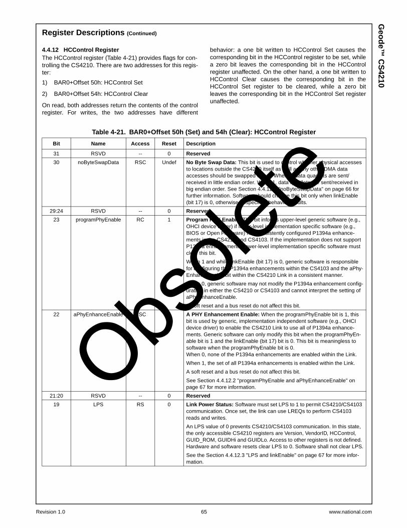
Revision 1.0 65 www.national.com
Geo
de™
CS
4210Register Descriptions (Continued)
4.4.12 HCControl RegisterThe HCControl register (Table 4-21) provides flags for con-trolling the CS4210. There are two addresses for this regis-ter:
1) BAR0+Offset 50h: HCControl Set
2) BAR0+Offset 54h: HCControl Clear
On read, both addresses return the contents of the controlregister. For writes, the two addresses have different
behavior: a one bit written to HCControl Set causes thecorresponding bit in the HCControl register to be set, whilea zero bit leaves the corresponding bit in the HCControlregister unaffected. On the other hand, a one bit written toHCControl Clear causes the corresponding bit in theHCControl Set register to be cleared, while a zero bitleaves the corresponding bit in the HCControl Set registerunaffected.
Table 4-21. BAR0+Offset 50h (Set) and 54h (Clear): HCControl Register
Bit Name Access Reset Description
31 RSVD -- 0 Reserved
30 noByteSwapData RSC Undef No Byte Swap Data: This bit is used to control whether physical accessesto locations outside the CS4210 itself as well as any other DMA dataaccesses should be swapped or not. When 0, data quadlets are sent/received in little endian order. When 1, data quadlets are sent/received inbig endian order. See Section 4.4.12.1 "noByteSwapData" on page 66 forfurther information. Software should change this bit only when linkEnable(bit 17) is 0, otherwise unspecified behavior results.
29:24 RSVD -- 0 Reserved
23 programPhyEnable RC 1 Program PHY Enable: This bit informs upper-level generic software (e.g.,OHCI device driver) if lower-level implementation specific software (e.g.,BIOS or Open Firmware) has consistently configured P1394a enhance-ments in the CS4210 and CS4103. If the implementation does not supportP1394a enhancements, lower-level implementation specific software mustclear this bit.
When 1 and while linkEnable (bit 17) is 0, generic software is responsiblefor configuring the P1394a enhancements within the CS4103 and the aPhy-EnhanceEnable bit within the CS4210 Link in a consistent manner.
When 0, generic software may not modify the P1394a enhancement config-uration in either the CS4210 or CS4103 and cannot interpret the setting ofaPhyEnhanceEnable.
A soft reset and a bus reset do not affect this bit.
22 aPhyEnhanceEnable RSC 0 A PHY Enhancement Enable: When the programPhyEnable bit is 1, thisbit is used by generic, implementation independent software (e.g., OHCIdevice driver) to enable the CS4210 Link to use all of P1394a enhance-ments. Generic software can only modify this bit when the programPhyEn-able bit is 1 and the linkEnable (bit 17) bit is 0. This bit is meaningless tosoftware when the programPhyEnable bit is 0.When 0, none of the P1394a enhancements are enabled within the Link.
When 1, the set of all P1394a enhancements is enabled within the Link.
A soft reset and a bus reset do not affect this bit.
See Section 4.4.12.2 "programPhyEnable and aPhyEnhanceEnable" onpage 67 for more information.
21:20 RSVD -- 0 Reserved
19 LPS RS 0 Link Power Status: Software must set LPS to 1 to permit CS4210/CS4103communication. Once set, the link can use LREQs to perform CS4103reads and writes.
An LPS value of 0 prevents CS4210/CS4103 communication. In this state,the only accessible CS4210 registers are Version, VendorID, HCControl,GUID_ROM, GUIDHi and GUIDLo. Access to other registers is not defined.Hardware and software resets clear LPS to 0. Software shall not clear LPS.
See the Section 4.4.12.3 "LPS and linkEnable" on page 67 for more infor-mation.
Obsole
te

www.national.com 66 Revision 1.0
Geo
de™
CS
4210 Register Descriptions (Continued)
4.4.12.1 noByteSwapDataThe 1394 bus is quadlet based big endian. By convention,when quadlets are sent in big endian order, the leftmostbyte (bits [31:24]) of a quadlet is sent first. When sent in lit-tle endian order, the right most byte (bits [7:0]) is sent firstwith the leftmost bit of each byte sent first.
When the CS4210 sends/receives a packet, the headerinformation is always sent/received in big endian order(leftmost byte first). Header information is composed of asequence of quadlets which is invariant over big and littleendian system.
When the HCControl.noByteSwapData bit is not set, dataquadlets are sent/received in little endian order and whenHCControl.noByteSwapData is set, data quadlets are sent/received in big endian order. The data quadlets as classi-fied by the OHCI transaction codes (tcodes) that are sub-ject to swap are:
1) Any data quadlet covered by data CRC (tcodes 1h, 7h,9h, Ah, and Bh).
2) The data quadlet in a quadlet write request (tcode 0h).
3) The data quadlet in a quadlet read response (tcode6h).
Since the cycle_time is self contained within the CS4210, itis never byte-swapped regardless of the setting of thenoByteSwapData bit.
The data in a PHY packet (identified internally with tcodeEh) is not byte swapped for send or receive.
Note: Due to some confusion regarding this bit, an expla-nation and some examples are available on theOpenHCI FTP site.
18 postedWriteEnable RSC Undef Posted Write Enable: This bit is used to enable (1) or disable (0) physicalposted writes. When disabled (0), physical writes are handled but areposted and instead are ack’ed with ack_pending.
Software should change this bit only when linkEnable (bit 17) is 0, other-wise unspecified behavior results. See Section 3.6 "Physical Requests" onpage 26 for information about posted writes.
17 linkEnable RSU 0 Link Enable: Software must set this bit to 1 when the system is ready tobegin operation and then force a bus reset. This bit is necessary to keepother nodes from sending transactions before the local system is ready.
When this bit is clear the CS4210 is logically and immediately disconnectedfrom the 1394 bus. The link will not process or interpret any packetsreceived from the CS4103, nor will it generate any bus requests. However,the link will access CS4103 registers via the CS4103 control register.
This bit is cleared to 0 by a hardware reset or software reset, and must notbe cleared by software. Software must not set the linkEnable bit until theConfiguration ROM mapping register (Section 4.4.9 on page 63) is valid.
16 softReset RSU ** Soft Reset: When set to 1, the CS4210’s state is reset, all FIFO’s areflushed and all CS4210 OHCI registers are set to their hardware reset val-ues unless otherwise specified. Registers outside of the OpenHCI realm(i.e., PCI and NSC defined registers) are not affected.
**The read value of this bit is 1 while a soft reset or a hard reset is inprogress. The read value of this bit is 0 when neither a soft reset nor hardreset are in progress. Software can use the value of this bit to determinewhen a reset has completed and the CS4210 is safe to operate.
15:0 RSVD -- 0 Reserved
Table 4-21. BAR0+Offset 50h (Set) and 54h (Clear): HCControl Register (Continued)
Bit Name Access Reset Description
Obsole
te
Revision 1.0 67 www.national.com
Geo
de™
CS
4210Register Descriptions (Continued)
4.4.12.2 programPhyEnable and aPhyEnhanceEnableAfter a hardware or software reset, system software mustensure that the CS4210 and the CS4103 are set to a con-sistent, compatible set of P1394a enhancements. The pro-gramPhyEnable and aPhyEnhanceEnable bits areprovided to enable software to accomplish this task. Sincedifferent levels of software may be responsible for ensuringthis setup, the programPhyEnable bit is defined to allowcommunication between implementation specific lower-level software (e.g., BIOS or Open Firmware) and generic,implementation independent upper-level software (e.g.,OHCI device driver). If generic software reads this bit as a1, it is responsible for configuring the P1394a enhance-ments in both the CS4210 and CS4103 in a consistentmanner (either all enhancements enabled or all enhance-ments disabled). A 0 value for this bit informs the upper-level system software that no further changes to theP1394a configurations of the CS4210 and CS4103 are per-mitted since either:
1) Lower-level software has previously performed initial-ization appropriate to the CS4210 capabilities, or
2) The link has hardwired P1394a capabilities to matchthe CS4103. Note that this bit is only a software flagand does not control any CS4210 functionality.
The programPhyEnable bit may be read-only, returning azero value, if upper-level software is not involved in theconfiguration of P1394a enhancements for the CS4210and CS4103. This is appropriate when the CS4210 andCS4103 are hardwired with compatible settings or whenlower-level software consistently configures both theCS4210 and CS4103. To allow the possibility for upper-level software control of P1394a enhancements, program-PhyEnable should be implemented as read/clear with ahardware reset value of 1. Software should clear program-PhyEnable once the CS4210 and CS4103 have been pro-grammed consistently by either lower-level or upper-levelsoftware. When programPhyEnable is set to 1, the aPhy-EnhanceEnable bit allows generic software to enable ordisable all P1394a enhancements within the CS4210 Link.A value of 1 for aPhyEnhanceEnable configures the Link touse all P1394a enhancements and is appropriate whensoftware has enabled all of the enhancements within theCS4103. Likewise, a value of 0 prevents the Link from
using any P1394a enhancements and is appropriate whensoftware has disabled all of the enhancements within theCS4103. Note that generic software must not attempt tomodify or interpret the setting of the aPhyEnhanceEnablebit if programPhyEnable contains a 0. The aPhyEnhan-ceEnable bit is read/set/clear and it resets to 0 for defaultcompatibility with legacy PHYs. These bits are accessiblefrom the nscControl register (BAR1+Offset 00h[14,13]).The aPhyEnhanceEnable bit can be initialized with theserial EEPROM.
4.4.12.3 LPS and linkEnableThere are three basic tasks and ensuing requirements withrespect to the Phy-Link interface:
1) Bootstrap of Open HCI.This requires a mechanism to configure the CS4210and CS4103 prior to receiving any packets or generat-ing any bus requests.
2) Recovery from a hung system.This requires a mechanism which places OpenHCI ina near pre-bootstrap condition, and allows the CS4210and CS4103 to get back into sync if required.
3) Power Management via Suspend/ResumeThis requires a mechanism to inform the CS4103 thatPhy-Link communication is no longer required and theCS4103 can suspend itself if no active ports remain.
To achieve proper behavior in satisfying these require-ments, software shall always assert the signals in the fol-lowing sequence: LPS, then linkEnable, then any otherindividual context enables or runs. The CS4210 behaviorwhen violating this order is undefined and can produceunreliable behavior. Table 4-22 illustrates the progressivefunctionality as these signals are asserted.
Following a hardware or software reset, LPS and linkEn-able are Off as shown in Step a (in Table 4-22). Softwareproceeds to enable the link power status (b) and whenSCLK has started, software can configure the CS4210 andCS4103 registers as listed in Step c (e.g., Self-ID receiveDMA registers). Setting linkEnable in step d enables someDMA function, and asserting contextControl.run (e) for theCS4210 contexts then yields full functionality.
Table 4-22. LPS and linkEnable Assertion
StepLPS
(BAR0+Offset 50h[19])linkEnable
(BAR0+Offset 50h[17]) contextControl.run Sequence Comments
a Off Off Off Initial State
b On Off Off Allows SCLK to start
c On Off Off Config Phy-Link registers
d On On Off Initiate Bus Reset
e On On Off Physical DMA/Cycle StartsOkay
f On On On Normal Operation
Obsole
te

www.national.com 68 Revision 1.0
Geo
de™
CS
4210 Register Descriptions (Continued)
4.4.13 Self-ID Buffer Pointer RegisterThe Self-ID Buffer Pointer register (Table 4-23) points tothe buffer the Self-ID packets are DMA’ed into during businitialization.
4.4.14 Self-ID Count RegisterThe Self-ID Count register (Table 4-24) keeps a count ofthe number of times the bus Self-ID process has occurred,flags Self-ID packet errors and keeps a count of theamount of Self-ID data in the Self-ID buffer.
Table 4-23. BAR0+Offset 64h: Self-ID Buffer Pointer Register
Bit Name Access Reset Description
31:11 selfIDBufferPtr RW Undef Self-ID Buffer Pointer: Contains the 2 KB aligned base address of thebuffer in host memory where received Self-ID packets are stored. The con-tents of this field are undefined after a chip reset.
10:0 RSVD -- 0 Reserved
Table 4-24. BAR0+Offset 68h: Self-ID Count Register
Bit Name Access Reset Description
31 selfIDError RU Undef Self-ID Error: When this bit is one, an error was detected during the mostrecent Self-ID packet reception. The contents of the Self-ID buffer are unde-fined. This bit is cleared after a Self-ID reception in which no errors aredetected. Note that an error can be a hardware error or a host bus writeerror.
30:24 RSVD -- 0 Reserved
23:16 selfIDGeneration RU Undef Self-ID Generation: The value in this field increments each time a busreset is detected. This field rolls over to 0 after reaching 255.
15:13 RSVD -- 0 Reserved
12:2 2selfIDSize RU Undef Quadlet Self-ID Size: This field indicates the number of quadlets that havebeen written into the Self-ID buffer for the current Self-ID Generation. Thisincludes the header quadlet and the Self-ID data. This field is cleared tozero as soon as a bus reset is detected.
1:0 RSVD -- 0 Reserved
Obsole
te

Revision 1.0 69 www.national.com
Geo
de™
CS
4210Register Descriptions (Continued)
4.4.15 IRMultiChanMask RegistersAn isochronous channel mask is used to enable packetreceives from up to 64 specified isochronous data chan-nels. Software enables receives for any number of isochro-nous channels by writing ones to the corresponding bits inthe:
1) BAR0+Offset 70h: IRMultiChanMaskHi Set
2) BAR0+Offset 78h: IRMultiChanMaskLo Set
To disable receives for any isochronous channels, softwarewrites ones to the corresponding bits in the:
1) BAR0+Offset 74h: IRMultiChanMaskHi Clear
2) BAR0+Offset 7Ch: IRMultiChanMaskLo Clear
A read of each IRMultiChanMask register shows whichchannels are enabled; a one for enabled, a zero for dis-abled. The IRMultiChanMask registers are not changed bya bus reset. The state of these registers is undefined fol-lowing a hard reset or soft reset.
Table 4-25. IRMultChanMask Registers
Bit Name Access Reset Description
BAR0+Offset 70h IRMultiChanMaskHi Set Register
31:0 IsochChannel[63:32] RSC Undef Isochronous Channels [63:32]: Bits [31:0] correspond to channels[63:32]. Set to one to enable receives to the corresponding channel.
BAR0+Offset 74h IRMultiChanMaskHi Clear Register
31:0 IsochChannel[63:32] RSC Undef Isochronous Channels [63:32]: Bits [31:0] correspond to channels[63:32]. Set to one to disable receives to the corresponding channel.
BAR0+Offset 78h IRMultiChanMaskLo Set Register
31:0 IsochChannel[31:0] RSC Undef Isochronous Channels [31:0]: Bits [31:0] correspond to channels [31:0].Set to one to enable receives to the corresponding channel.
BAR0+Offset 7Ch IRMultiChanMaskLo Clear Register
31:0 IsochChannel[31:0] RSC Undef Isochronous Channels [31:0]: Bits [31:0] correspond to channels [31:0].Set to one to disable receives to the corresponding channel.
Obsole
te

www.national.com 70 Revision 1.0
Geo
de™
CS
4210 Register Descriptions (Continued)
4.4.16 InterruptsThe CS4210 reports two classes of interrupts to the host:DMA interrupts and device interrupts. DMA interrupts aregenerated when DMA transfers complete (or are aborted).Device interrupts come directly from the remaining 1394Open HCI logic. For example, one of these interrupts couldbe sent in response to the asserting edge of cycleStart, asignal which indicates that a new isochronous cycle hasstarted.
The CS4210 contains two primary 32-bit registers to reportand control interrupts: IntEvent and IntMask. Both registershave two addresses: a “Set” address and a “Clear”address. For a write to either register, a “one” bit written tothe “Set” address causes the corresponding bit in the regis-ter to be set (excluding bits which are read-only), while a“one” bit written to the “Clear” address causes the corre-sponding bit to be cleared. For both addresses, writing a“zero” bit has no effect on the corresponding bit in the reg-ister.
The IntEvent register contains the actual interrupt requestbits. Each of these bits corresponds to either a DMA com-pletion event, or a transition on a device interrupt line. TheIntMask register is ANDed with the IntEvent register toenable selected bits to generate processor interrupts. Soft-ware writes to the IntEvent Clear register to clear interruptconditions reported in the IntEvent register.
A processor interrupt is generated when one or moreunmasked bits are set in the IntEvent register. Low-levelsoftware responds to the interrupt by reading the IntEventregister, then writing the value read to the IntEvent Clearregister. At this point the interrupt request is deasserted(assuming no new interrupt bit has been set). Software canproceed to process the reported interrupts in whatever pri-ority order it chooses, and is free to re-enable interrupts assoon as the IntEvent Clear register is written.
In addition, the CS4210 contains four secondary 32-bit reg-isters to report and control interrupts for isochronous trans-mit and receive contexts. Each register has two addresses:a “Set” address and a “Clear” address.
4.4.16.1 IntEvent RegisterThis register reflects the state of the various interruptsources from the 1394 Open HCI. The interrupt bits are setby an asserting edge of the corresponding interrupt signal,or by software by writing a one to the corresponding bit inthe IntEvent Set register. They are cleared by writing a oneto the corresponding bit in the IntEvent Clear register.
Reading the IntEvent Set register (BAR0+Offset 80h)returns the current state of the IntEvent register. Readingthe IntEvent Clear register (BAR0+Offset 84h) returns themasked version of the IntEvent register (IntEvent and Int-Mask).
Table 4-26. BAR0+Offset 80h (Set) and 84h (Clear): IntEvent Register
Bit Name Access Reset Description
31:27 RSVD -- 0 Reserved
26 phyRegRcvd RSCU Undef PHY Register Received: The CS4210 has received a PHY register databyte which can be read from the PHY control register (see Section 4.4.20"PHYControl Register" on page 77).
25 cycleTooLong RSCU Undef Cycle Too Long: If LinkControl.cycleMaster (BAR0+Offset E0h[21] is set,this indicates that an isochronous cycle lasted longer than the allotted time.For implementations with a discrete cycleTooLong timer, hardware isexpected to trigger this event no less than 115 seconds and no more than120 seconds after sending a cycle start packet unless a subaction gap orbus reset indication is first observed. LinkControl.cycleMaster is cleared bythis event.
24 unrecoverableError RSCU Undef Unrecoverable Error: This event occurs when the CS4210 encounters anyerror that forces it to stop operations on any or all of its subunits. For exam-ple, when a DMA context sets its contextControl.dead bit. While unrecover-ableError is set, all normal interrupts for the context(s) that caused thisinterrupt are blocked from being set.
23 cycleInconsistent RSC Undef Cycle Inconsistent: A cycle start was received that had an isochronouscycleTimer.seconds and isochronous cycleTimer.count different from thevalue in the IsochCycleTimer register (BAR0+Offset F0h, see Section4.4.21 "IsochCycleTimer Register" on page 77). The CS4210 indicates acycleInconsistent if a host initiated write changes the cycleSeconds orcycleCount fields of the cycleTimer register. For the effect of this conditionon isochronous transmit and receive, refer to Section 3.8.3 "IsochronousTransmit and Receive" on page 30.
22 cycleLost RSCU Undef Cycle Lost: A lost cycle is indicated when no cycle_start packet is sent/received between two successive cycleSynch events.
21 cycle64Seconds RSCU Undef Cycle 64 Seconds: Indicates that the 7th bit of the cycle second counterhas changed.
Obsole
te
Revision 1.0 71 www.national.com
Geo
de™
CS
4210Register Descriptions (Continued)
20 cycleSynch RSCU Undef Cycle Synchronous: Indicates that a new isochronous cycle has started.Set when the low order bit of the internal IsochCycleTimer.cycleCount(BAR0+Offset F0h[24:12]) toggles.
19 phy RSCU Undef Physical Layer: Generated when the CS4103 requests an interruptthrough a status transfer.
18 RSVD -- 0 Reserved
17 busReset RSCU Undef Bus Reset: Indicates that the CS4103 has entered bus reset mode. SeeSection 4.4.16.2 "Bus Reset" on page 72 for information on when to clearthis interrupt.
16 selfIDcomplete RSCU Undef Self-ID Complete: A Self-ID packet stream has been received. Is set at theend of the bus initialization process if LinkControl.rcvSelfID (BAR0+OffsetE0h[9]) is set. This bit is turned off simultaneously when IntEvent.busReset(bit 17) is turned on.
15:10 RSVD -- 0 Reserved
9 lockRespErr RSCU Undef Lock Response Error: Indicates that the CS4210 attempted to return alock response for a lock request to a serial bus register described in Section4.4.4 "Autonomous CSR Resources" on page 60, but did not receive anack_complete after exhausting all permissible retries.
8 postedWriteErr RSCU Undef Posted Write Error: Indicates that a host bus error occurred while theCS4210 was trying to write a 1394 write request, which had already beengiven an ack_complete, into system memory. The 1394 destination offsetand sourceID are available in the PostedWriteAddress register described inSection 3.7.7 "Posted Write Error" on page 29.
7 isochRx RU Undef Isochronous Receive DMA interrupt: Indicates that one or more isochro-nous receive contexts have generated an interrupt. This is not a latchedevent, it is the OR’ing all bits in (IsochRxIntEvent and IsochRxIntMask). TheIsochRxIntEvent register indicates which contexts have interrupted. SeeSection 4.4.16.6 "IsochRxIntEvent Register" on page 74.
6 isochTx RU Undef Isochronous Transmit DMA interrupt: Indicates that one or more isochro-nous transmit contexts have generated an interrupt. This is not a latchedevent, it is the OR’ing all bits in (isochTxIntEvent and isochTxIntMask). TheisochTxIntEvent register indicates which contexts have interrupted. SeeSection 4.4.16.4 "IsochTxIntEvent Register" on page 73.
5 RSPkt RSCU Undef Receive Response Packet: Indicates that a packet was sent to an asyn-chronous receive response context buffer and the descriptor’s xferStatusand resCount fields have been updated. This differs from ARRS (bit 3)since RSPkt is a per-packet completion indication and ARRS is a per-com-mand descriptor (buffer) completion indication. AR Response buffers maycontain more than one packet.
4 RQPkt RSCU Undef Receive Request Packet: Indicates that a packet was sent to an asynchro-nous receive request context buffer and the descriptor’s xferStatus and res-Count fields have been updated. This differs from ARRQ (bit 2) sinceRQPkt is a per-packet completion indication and ARRQ is a per-commanddescriptor (buffer) completion indication. AR Request buffers may containmore than one packet.
3 ARRS RSCU Undef Asynchronous Receive Response DMA Interrupt: This bit is condition-ally set upon completion of an ARDMA Response context commanddescriptor.
2 ARRQ RSCU Undef Asynchronous Receive Request DMA Interrupt: This bit is conditionallyset upon completion of an ARDMA Request context command descriptor.
1 respTxComplete RSCU Undef Asynchronous Response Transmit DMA Interrupt: This bit is condition-ally set upon completion of an ATDMA response OUTPUT_LAST* com-mand.
0 reqTxComplete RSCU Undef Asynchronous Request Transmit DMA Interrupt: This bit is conditionallyset upon completion of an ATDMA request OUTPUT_LAST* command.
Table 4-26. BAR0+Offset 80h (Set) and 84h (Clear): IntEvent Register (Continued)
Bit Name Access Reset Description
Obsole
te
www.national.com 72 Revision 1.0
Geo
de™
CS
4210 Register Descriptions (Continued)
4.4.16.2 Bus ResetWhen a bus reset occurs and the busReset interrupt is setto one, the selfIDComplete (BAR0+Offset 80h[16]) inter-rupt is simultaneously cleared to 0. The CS4210 preventssoftware from clearing the busReset interrupt bit during theSelf-ID phase of bus initialization. Software must take pre-cautions regarding the asynchronous transmit contextsbefore clearing this interrupt. Refer to Section 3.8 "BusResets" on page 30 for further details.
4.4.16.3 IntMask RegisterThe bits in the IntMask register have the same format asthe IntEvent register, with the addition of masterIntEnable(bit 31). A one bit in the IntMask register enables the corre-sponding IntEvent register bit to generate a processorinterrupt. A zero bit in IntMask disables the correspondingIntEvent register bit from generating a processor interrupt.
A bit is set in the IntMask register by writing a one to thecorresponding bit in the IntMask Set address and clearedby writing a one to the corresponding bit in the IntMaskClear address. If masterIntEnable is 0, all interrupts aredisabled regardless of the values of all other bits in the Int-Mask register. The value of masterIntEnable has no effecton the value returned by reading the IntEvent Clear; even ifmasterIntEnable is 0, reading IntEvent Clear returns(IntEvent and IntMask) as described earlier in Section4.4.16 "Interrupts" on page 70.
On a reset, the IntMask.masterIntEnable bit (31) is set to 0and the value of all other bits is undefined.
1) BAR0+Offset 88h: IntMask Set
2) BAR0+Offset 8Ch: IntMask Clear
Table 4-27. BAR0+Offset 88h (Set) and 8Ch (Clear): IntMask Register
Bit Name Access Reset Description
31 masterIntEnable RSC 0 Master Interrupt Enable: If set, external interrupts are generated inaccordance with the IntMask register. If clear, no external interrupts aregenerated regardless of the IntMask register settings.
30:27 RSVD -- 0
26 phyRegRcvdIntEn RSC Undef Interrupt Events: A one bit enables the corresponding IntEvent registerbit to generate a processor interrupt. A zero bit disables the correspondingIntEvent register bit from generating a processor interrupt. See Table 4-26"BAR0+Offset 80h (Set) and 84h (Clear): IntEvent Register" on page 70.
25 cycleTooLongIntEn RSC Undef
24 unrecoverableError-IntEn
RSC Undef
23 cycleInconsis-tentIntEn
RSC Undef
22 cycleLostIntEn RSC Undef
21 cycle64SecondsIntEn RSC Undef
20 cycleSynchIntEn RSC Undef
19 phyIntEn RSC Undef
18 RSVD -- 0
17 busResetIntEn RSC Undef
16 selfIDcompleteIntEn RSC Undef
15:10 RSVD -- 0
9 lockRespErrIntEn RSC Undef
8 postedWriteErrIntEn RSC Undef
7 isochRxIntEn RSC Undef
6 isochTxIntEn RSC Undef
5 RSPktIntEn RSC Undef
4 RQPktIntEn RSC Undef
3 ARRSIntEn RSC Undef
2 ARRQIntEn RSC Undef
1 respTxCompleteIntEn RSC Undef
0 reqTxCompleteIntEn RSC Undef
Obsole
te

Revision 1.0 73 www.national.com
Geo
de™
CS
4210Register Descriptions (Continued)
4.4.16.4 IsochTxIntEvent RegisterThere are two 32-bit registers to report isochronous trans-mit context interrupts: IsochTxIntEvent and IsochTxInt-Mask. Both registers are set and clear (Tables 4-28 and 4-29). For all four addresses, writing a zero bit has no effecton the corresponding bit in the register.
The IsochTxIntEvent register contains the actual interruptrequest bits. Each of these bits corresponds to a DMAcompletion event for the indicated isochronous transmitcontext. The IsochTxIntMask register is ANDed with theIsochTxIntEvent register to enable selected bits to gener-ate processor interrupts. If IsochTxIntMask and IsochTx-IntEvent are not zero, then the IntEvent.IsochTxIntn bit isset to one, and if enabled via the IntMask register it gener-ates a processor interrupt. A software write to the IsochTx-IntEvent Set register can therefore cause an interrupt (if nototherwise masked). A software write to the IsochTx-IntEvent Clear register clears interrupt conditions reportedin the IsochTxIntEvent register.
Reading the IsochTxIntEvent Set register returns the cur-rent state of the IsochTxIntEvent register. Reading theIsochTxIntEvent Clear register returns the masked version
of the IsochTxIntEvent register (IsochTxIntEvent andIsochTxIntMask).
This IsochTxIntEvent register reflects the interrupt state ofthe isochronous transmit contexts. An interrupt is gener-ated on behalf of an isochronous transmit context if anOUTPUT_LAST DMA command completes and its “i” fieldis set to 11b (interrupt always). Upon determining that theIntEvent.IsochTx interrupt has occurred, software cancheck the IsochTxIntEvent register to determine which con-text(s) caused the interrupt.
4.4.16.5 IsochTxIntMask RegisterThe bits in the IsochTxIntMask register (Table 4-29) havethe same format as the IsochTxIntEvent register. Setting abit in this register enables the corresponding bit in theIsochTxIntEvent register. Setting a bit in this register isdone by setting the bit in the IsochTxIntMask Set register(BAR0+Offset 98h) and cleared by writing a one to the cor-responding bit in the IsochTxIntMask Clear register(BAR0+Offset 9Ch). Bits for all unimplemented contextsread as 0’s. Software can use this register to determinewhich contexts are supported by writing to it with all 1’s,then reading it back. Contexts with a 1 are implemented,and those with a 0 are not.
Table 4-28. BAR0+Offset 90h (Set) and 94h (Clear): IsochTxIntEvent Register
Bit Name Access Reset Description
31:8 RSVD -- 0 Reserved
7 isochTxInt7 RSCU Undef Isochronous Transmit Context Interrupt Event: Set to one when the cor-responding isochronous transmit context interrupts and the interrupt mask(BAR0+Offset 98h) is enabled.
6 isochTxInt6
5 isochTxInt5
4 isochTxInt4
3 isochTxInt3
2 isochTxInt2
1 isochTxInt1
0 isochTxInt0
Table 4-29. BAR0+Offset 98h (Set) and 9Ch (Clear): IsochTxIntMask Register
Bit Name Access Reset Description
31:8 RSVD -- 0 Reserved
7 isochTxIntMask7 RSC Undef Isochronous Transmit Context Interrupt Mask: Set to one enables thecorresponding bit in the IsochTxintEvent register (BAR0+Offset 90h).6 isochTxIntMask6
5 isochTxIntMask5
4 isochTxIntMask4
3 isochTxIntMask3
2 isochTxIntMask2
1 isochTxIntMask1
0 isochTxIntMask0
Obsole
te
www.national.com 74 Revision 1.0
Geo
de™
CS
4210 Register Descriptions (Continued)
4.4.16.6 IsochRxIntEvent RegisterThere are two 32-bit registers to report isochronous receivecontext interrupts: IsochRxIntEvent and IsochRxIntMask.Both registers are set and clear. For all four addresses,writing a “zero” bit has no effect on the corresponding bit inthe register. The IsochRxIntEvent register contains theactual interrupt request bits. Each of these bits corre-sponds to a DMA completion event for the indicated isoch-ronous receive context. The IsochRxIntMask register isANDed with the IsochRxIntEvent register to enableselected bits to generate processor interrupts. If (IsochRx-IntMask and IsochRxIntEvent) are not zero, then the Isoch-RxIntn bit is set to one, and if enabled via the IntMaskregister it generates a processor interrupt. A software writeto the IsochRxIntEvent Set register can therefore cause aninterrupt (if not otherwise masked). A software write to theIsochRxIntEvent Clear register clears interrupt conditionsreported in the IsochRxIntEvent register. Reading the Iso-chRxIntEvent Set register returns the current state of theIsochRxIntEvent register. Reading the IsochRxIntEventClear register returns the masked version of the IsochRx-
IntEvent register (IsochRxIntEvent and IsochRxIntMask).The IsochRxIntEvent register reflects the interrupt state ofthe isochronous receive contexts. An interrupt is generatedon behalf of an isochronous receive context if a final com-mand of a DMA descriptor block completes and its i bits areset to 11b (interrupt always). Upon determining that theIsochRx interrupt has occurred, software can check theIsochRxIntEvent register to determine which context(s)caused the interrupt.
4.4.16.7 IsochRxIntMask RegisterThe bits in the IsochRxIntMask register have the same for-mat as the IsochRxIntEvent register. Setting a bit in thisregister enables the corresponding bit in the IsochRxInt-Mask Set register and is cleared by writing a one to the cor-responding bit in the IsochRxIntMask Clear register. Bitsfor all unimplemented contexts read as 0’s. Software canuse this register to determine which contexts are supportedby writing to it with all 1’s then reading it back. Contextswith a 1 are implemented, and those with a 0 are not.
Table 4-30. BAR0+Offset A0h (Set) and A4h (Clear): IsochRxIntEvent Register
Bit Name Access Reset Description
31:8 RSVD -- 0 Reserved
7 isochRxInt7 RSC Undef Isochronous Receive Contexts Interrupt Event: Set to one when the cor-responding isochronous receive context interrupts and the Interrupt Mask isenabled.
6 isochRxInt6
5 isochRxInt5
4 isochRxInt4
3 isochRxInt3
2 isochRxInt2
1 isochRxInt1
0 isochRxInt0
Table 4-31. BAR0+Offset A8h (Set) and ACh (Clear): IsochRxIntMask Register
Bit Name Access Reset Description
31:8 RSVD -- 0 Reserved
7 isochRxIntMask7 RSC Undef Isochronous Receive Contexts Interrupt Mask Set: Set to one enablesthe corresponding bit in the IsochRxIntEvent Register.6 isochRxIntMask6
5 isochRxIntMask5
4 isochRxIntMask4
3 isochRxIntMask3
2 isochRxIntMask2
1 isochRxIntMask1
0 isochRxIntMask0
Obsole
te

Revision 1.0 75 www.national.com
Geo
de™
CS
4210Register Descriptions (Continued)
4.4.17 Fairness Control RegisterThis register (Table 4-32) provides a mechanism by whichsoftware can direct the CS4210 to transmit multiple asyn-chronous request packets during a fairness interval asspecified in P1394a specification.
4.4.18 LinkControl RegisterThis register (Table 4-33) provides the control flags thatenable and configure the link core protocol and controls forthe receiver and cycle timer. This register is set(BAR0+Offset E0h) and clear (BAR0+Offset E4h). Onread, both addresses return LinkControl.
Table 4-32. BAR0+Offset DCh: Fairness Control Register
Bit Name Access Reset Description
31:8 RSVD -- 0 Reserved
7:0 pri_req RW HW =Undef
SW/Bus= N/A
Priority Arbitration Request: This field specifies the maximum number ofpriority arbitration requests for asynchronous request packets that the link ispermitted to make to the CS4103 during a fairness interval. A pri_req valueof 00h is equivalent to the behavior specified by the IEEE 1394-1995 speci-fication.
Table 4-33. BAR0+Offset E0h (Set) and E4h (Clear): LinkControl Register
Bit Name Access Reset Description
32:21 RSVD -- 0 Reserved
22 cycleSource RSCor R
HW = 0
SW = NoChange
Cycle Source: When one, the cycle timer uses an external source to deter-mine when to increment cycleCount (BAR0+Offset F0h[24:12]). WhencycleCount is incremented, cycleOffset (BAR0+Offset F0h[11:0]) is reset to0. If cycleOffset reaches 3071 before an external event occurs, it remains at3071 until the external signal is received and is then reset to 0. When thecycleSource bit is zero, the CS4210 rolls the cycle timer over when thetimer reaches 3072 cycles of the 24.576 MHz clock (8 kHz). CycleSourcehas an effect only when cycleMaster (bit 21) is enabled. A hardware resetclears to 0. A software reset has no effect.
21 cycleMaster RSCU Undef Cycle Master: When one and the CS4103 has notified the CS4210 that it isroot, the CS4210 generates a cycle start packet every time the cycle timerrolls over, based on the setting of the cycleSource bit (bit 22). When zero,the CS4210 accepts received cycle start packets to maintain synchroniza-tion with the node which is sending them. This bit is automatically zeroedwhen the IntEvent.cycleTooLong event occurs and cannot be set until theIntEvent.cycleTooLong bit (BAR0+Offset 80h[25]) is cleared.
20 cycleTimerEnable RSC Undef Cycle Timer Enable: When one, the cycle timer offset counts cycles of the24.576 MHz clock and rolls over at the appropriate time based on the set-tings of the above bits. When zero, the cycle timer offset will not count.
19:11 RSVD -- 0 Reserved
10 rcvPhyPkt RSC Undef Receive Physical Layer Packet: When one, the receiver accepts incomingCS4103 packets into the AR request context if the AR request context isenabled. This does not control either the receipt of self-identification pack-ets during the Self-ID phase of bus initialization or the queuing of synthe-sized bus reset packets in the ARDMA Request Context buffer (see Section3.8 "Bus Resets" on page 30). This does control receipt of any self- identifi-cation packets received outside of the Self-ID phase of bus initialization.
9 rcvSelfID RSC Undef Receive Self-ID: When one, the receiver accepts incoming self-identifica-tion packets. Before setting this bit to one, software must ensure that theselfIDBufferPtr register bits (BAR0+Offset 64h[31:11]) contains a validaddress.
8:0 RSVD -- 0 Reserved
Obsole
te

www.national.com 76 Revision 1.0
Geo
de™
CS
4210 Register Descriptions (Continued)
4.4.19 Node ID and Status RegisterThis register contains the CSR address for the node onwhich this chip resides. The 16-bit combination of busNum-ber and nodeNumber is referred to as the Node ID. Thisregister is written autonomously and atomically by theCS4210 with the value in CS4103’s base register atAddress 00h following the self-identification phase of bus
initialization. Although IntEvent.phyRegRcvd (BAR0+Offset80h[26]) is not set when the contents of CS4103’s baseregister at Address 00h are written here, software can usethe IntEvent.selfIDComplete (BAR0+Offset 80h[16]) inter-rupt to detect that the self-identification phase has com-pleted and can then check for a new valid Node ID.
Table 4-34. BAR0+Offset E8h: Node ID and Status Register
Bit Name Access Reset Description
31 iDValid RU 0 ID Valid: This bit indicates whether or not the CS4210 has a valid nodenumber. It is cleared when the bus reset state is detected and set againwhen the CS4210 receives a new node number from the CS4103.
If iDValid is clear, software should not set ContextControl.run for either ofthe ATDMA contexts (request and response).
30 root RU 0 Root: This bit is set during the bus reset process if the CS4103 is root.
29:28 RSVD -- 0 Reserved
27 CPS RU 0 Cable Power Status: Set if the CS4103 is reporting that cable power statusis OK (VP 8V).
26:16 RSVD -- 0 Reserved
15:6 busNumber RWU 3FFh Bus Number: This number is used to identify the specific 1394 bus thisnode belongs to when multiple 1394-compatible buses are connected via abridge. This field is set to 3FFh on a bus reset.
5:0 nodeNumber RU Undef Node Number: This number is the physical node number established bythe CS4103 during self-identification. It is automatically set to the valuereceived from the CS4103 after the self-identification phase. If the CS4103sets the nodeNumber to 63, software should not set ContextControl.run foreither of the ATDMA contexts (request and response).
Obsole
te

Revision 1.0 77 www.national.com
Geo
de™
CS
4210Register Descriptions (Continued)
4.4.20 PHYControl RegisterThe PHYControl register (Table 4-35) is used to read orwrite a CS4103 register. To read a register, the address ofthe register is written to the regAddr field along with a 1 inthe rdReg bit. When the read request has been sent to theCS4103 (through the LREQ pin), the rdReg bit is cleared to0. When the CS4103 returns the register, the rdDone bittransitions to 1 and the IntEvent.phyRegRcvd interrupt(BAR0+Offset 80h[26]) is set. The address of the registerreceived is placed in the rdAddr field and the contents inthe rdData field. Software must not issue a read of CS4103register 0. The most recently available contents of this reg-ister is reflected in the NodeID register (see Section 4.4.19"Node ID and Status Register" on page 76). To write to aCS4103 register, the address of the register is written tothe regAddr field, the value to write to the wrData field, anda 1 to the wrReg bit. The wrReg bit is cleared when thewrite request has been transferred to the CS4103. Soft-ware must serialize all CS4103 register reads and writes.
Only after the current CS4103 register read or write com-pletes may software issue a different CS4103 register reador write.
4.4.21 IsochCycleTimer RegisterThe IsochCycleTimer register (Table 4-36) is a read/writeregister that shows the current cycle number and offset.The cycle timer register is split up into three fields. Thelower order 12 bits are the cycle offset, the middle 13 bitsare the cycle count, and the upper order 7 bits count time inseconds. When the CS4210 is cycle master, this register istransmitted with the cycle start message. When theCS4210 is not the cycle master, this register is loaded withthe data field in each incoming cycle start. In the event thatthe cycle start message is not received, the fields continueincrementing on their own (when cycleTimerEnable is setin the LinkControl register, BAR0+Offset E0h[20]) to main-tain a local time reference.
Table 4-35. BAR0+Offset ECh: PHYControl Register
Bit Name Access Reset Description
31 rdDone RU Undef Read Done: rdDone is cleared to 0 by the CS4210 when either rdReg orwrReg is set to 1. This bit is set to 1 when a register transfer is receivedfrom the CS4103.
30:28 RSVD -- 0 Reserved
27:24 rdAddr RU Undef Read Address: This is the address of the register most recently receivedfrom the CS4103.
23:16 rdData RU Undef Read Data: Contains the data read from the CS4103 register at rdAddr.
15 rdReg RWU 0 Read Register: Set rdReg to initiate a read request to a CS4103 register.This bit is cleared when the read request has been sent. The wrReg bitmust not be set while the rdReg bit is set.
14 wrReg RWU 0 Write Register: Set wrReg to initiate a write request to a CS4103 register.This bit is cleared when the write request has been sent. The rdReg bitmust not be set while the wrReg bit is set.
13:12 RSVD -- 0 Reserved
11:8 regAddr RW Undef Register Address: regAddr is the address of the CS4103 register to bewritten or read.
7:0 wrData RWU Undef Write Data: This is the contents to be written to a CS4103 register. Ignoredfor a read.
Table 4-36. BAR0+Offset F0h: IsochCycleTimer Register
Bit Name Access Reset Description
31:25 cycleSeconds RWU N/A Cycle Seconds: This field counts seconds (cycleCount rollovers) modulo128.
24:12 cycleCount RWU N/A Cycle Count: This field counts cycles (cycleOffset rollovers) modulo 8000.
11:0 cycleOffset RWU N/A Cycle Offset: This field counts 24.576 MHz clocks modulo 3072, (i.e., 125µs). If an external 8 kHz clock configuration is being used, cycleOffset is setto 0 at each tick of the external clock.
Obsole
te

www.national.com 78 Revision 1.0
Geo
de™
CS
4210 Register Descriptions (Continued)
4.4.22 Asynchronous Request Filter RegistersThe CS4210 allows for selective access to host memoryand the Asynchronous Receive Request context so thatsoftware can maintain host memory integrity. The selectiveaccess is provided by two sets of registers: PhysRequest-Filter and AsyncRequestFilter. These registers allowaccess to physical memory and the AR Request context ona nodeID basis. The request filters are not applied to qua-dlet read requests directed at the Config ROM (includingthe ConfigROM header, BusID, Bus Options, and GlobalUnique ID registers) nor to accesses directed to the isoch-ronous resource management registers. When the link isenabled, access by any node to the first 1K of CSR configROM is enabled (see Section 4.4.5 "Configuration ROMHeader Register" on page 61). The Asynchronous RequestFilters do not have any effect on Asynchronous Responsepackets. When a request is received by the CS4210 fromthe 1394 bus and that request does not access the first 1Kof CSR config ROM on the CS4210, then the sourceID isused to index into the AsyncRequestFilter. If the corre-sponding bit in the AsyncRequestFilter is set to 0, then
requests from that device are not enabled; there is no ack_sent, and the requests are ignored by the CS4210. If, how-ever, the bit is set to 1, the requests are accepted and pro-cessed according to the address of the request and thesetting of the PhysicalRequestFilter register (BAR0+Offset110h, see Section 4.4.23 "Physical Request Filter Regis-ters" on page 79). Requests to offsets above0000_FFFF_FFFFh, with the exception of offsets handledphysically as described in Section 3.6 "Physical Requests"on page 26, are always sent to the Asynchronous RequestReceive DMA context. If the AR Request DMA context isnot enabled, then the CS4210 ignores the request. Theseregisters are set and clear. If bit asyncReqResourceN isset, then requests with a sourceID of either {3FFh, #N} or{busID, #N} are accepted. If the asyncReqResourceAll bitis set in AsyncRequestFilterHi, requests from all bus nodesincluding those on the local bus are accepted. Reading theAsyncRequestFilter registers returns their current state. AllasyncReqResourceN bits in the AsyncRequestFilter regis-ter are cleared to 0 on a 1394 bus reset.
Table 4-37. BAR0+Offset 100h (Set) and 104h (Clear): AsyncRequestFilterHi Register
Bit Name Access Reset Description
31 asyncReqRe-sourceAll
RSCU 0 Asynchronous Requests Resource All: If set to one, all asynchronousrequests received by the CS4210 from all bus nodes (including the localbus) are accepted, and the values of all asyncReqResourceN bits areignored. A bus reset does not affect the value of the asyncReqResourceAllbit.
30:0 asyncReqRe-sourceN
RSCU 00h Asynchronous Requests Resource [62:32]: If set to one for local busnode number N, asynchronous requests received by the CS4210 from thatnode are accepted. All asyncReqResourceN bits are cleared to zero whena bus reset occurs.
Table 4-38. BAR0+Offset 108h (Set) and 10Ch (Clear): AsyncRequestFilterLo Register
Bit Name Access Reset Description
31:0 asyncReqRe-sourceN
RSCU 00h Asynchronous Requests Resource [31:0]: If set to one for local bus nodenumber N, asynchronous requests received by the CS4210 from that nodeare accepted. All asyncReqResourceN bits are cleared to zero when a busreset occurs.Obsole
te
Revision 1.0 79 www.national.com
Geo
de™
CS
4210Register Descriptions (Continued)
4.4.23 Physical Request Filter RegistersIf an asynchronous request is allowed from a node, and theoffset is 0000_FFFF_FFFFh, the sourceID of the request isused as an index into the PhysicalRequestFilter. If the cor-responding bit in the PhysicalRequestFilter is set to 0, thenthe request is forwarded to the Asynchronous RequestReceive DMA context. If, however, the bit is set to 1, thenthe request is sent to the physical response unit. (Note thatwithin the physical range, lock transactions and block trans-actions with a non-zero extended tcode are always for-warded to the Asynchronous Request Receive DMAcontext (see Section 3.6 "Physical Requests" on page 26.).This register is set and clear. If bit physReqResourceN is
set, then requests with a sourceID of either {3FFh, #n} or{busID, #n} (where n is the node number) are accepted. Ifthe physReqResourceAllBuses bit is set in PhysicalRe-questFilterHi, physical requests from any device on anyother bus are accepted (bus number other than 3FFh andbusID). Physical requests that are rejected by the Physical-RequestFilter are sent to the AR Request DMA context ifthe AR Request DMA context is enabled. If it is disabled,then the CS4210 ignores the requests. Reading the Physi-calRequestFilter registers returns their current state. Allbits in the PhysicalRequestFilter are set to 0 on a 1394 busreset.
Table 4-39. BAR0+Offset 110h (Set) and 114h (Clear): PhysicalRequestHi Register
Bit Name Access Reset Description
31 physReqRe-sourceAllBuses
RSCU 0 Asynchronous Physical Requests Resource All Buses: If set to one, allasynchronous physical requests received by the CS4210 from non-localbus nodes are accepted.
30:0 physReqResourceN RSCU 00h Asynchronous Physical Requests Resource [62:32]: If set to one forlocal bus node number N, then asynchronous physical requests received bythe CS4210 from that node are accepted.
Table 4-40. BAR0+Offset 118h (Set) and 11Ch (Clear): PhysicalRequestLo Register
Bit Name Access Reset Description
31:0 physReqResourceN RSCU 00h Asynchronous Physical Requests Resource [31:0]: If set to one for localbus node number N, then asynchronous physical requests received by theCS4210 from that node are accepted.
Obsole
te

www.national.com 80 Revision 1.0
Geo
de™
CS
4210 Register Descriptions (Continued)
4.4.24 Asynchronous Request/Response TransmitEach ATDMA context (request and response) has two reg-isters: CommandPtr and ContextControl. CommandPtr isused by software to tell the CS4210 where the DMA con-text program begins. ContextControl is used by software tocontrol the context’s behavior, and is used by hardware toindicate current status.
4.4.24.1 Async Request Transmit Context ControlRegister
The ContextControl Set/Clear registers contain bits thatcontrol options, operational state and status for the DMAcontext. Software can set selected bits by writing ones tothe corresponding bits in the ContextControl Set register.Software can clear selected bits by writing ones to the cor-
responding bits in the ContextControl Clear register. It isnot possible for software to set some bits and clear othersin an atomic operation. A read from either register returnsthe same value.
4.4.24.2 Async Request Transmit Command PointerRegister
Software initializes CommandPtr.descriptorAddress to con-tain the address of the first descriptor block that theCS4210 accesses when software enables the context bysetting ContextControl.run. Software also initializes Com-mandPtr.Z to indicate the number of descriptors in the firstdescriptor block. Software only writes to this register whenboth ContextControl.run and ContextControl.active arezero.
Table 4-41. BAR0+Offset 180h (Set) and 184h (Clear): AsyncReqTxContextControl Register
Bit Name Access Reset Description
31:16 RSVD -- 0 Reserved
15 run RSCU 0 Run: The run bit is set by software to enable descriptor processing for acontext and cleared by software to stop descriptor processing. The CS4210only clears this bit on a hardware or software reset. See Section 3.3.2.1"ContextControl.run" on page 21 for details.
14:13 RSVD -- 0 Reserved
12 wake RSU Undef Wake: Software sets this bit to 1 to cause the CS4210 to continue orresume descriptor processing. The CS4210 clears this bit on every descrip-tor fetch. See Section 3.3.2.2 "ContextControl.wake" on page 21 for details.
11 dead RU 0 Dead: The CS4210 sets this bit when it encounters a fatal error. TheCS4210 clears this bit when software clears the run bit. See Section 3.3.2.4"ContextControl.dead" on page 21 for details.
10 active RU 0 Active: The CS4210 sets this bit to 1 when it is processing descriptors. SeeSection 3.3.2.3 "ContextControl.active" on page 21 for details.
9:5 RSVD -- 0 Reserved
4:0 event code RU Undef Event Code: Following an OUTPUT_LAST* command, the receivedack_code or an “evt_” error code is indicated in this field. Possible valuesare: ack_complete, ack_pending, ack_busy_X, ack_busy_A, ack_busy_B,ack_data_error, ack_type_error, evt_tcode_err, evt_missing_ack,evt_underrun, evt_descriptor_read, evt_data_read,evt_timeout,evt_flushed, and evt_unknown.
Table 4-42. BAR0+Offset 18Ch: AsyncReqTxCommandPtr Register
Bit Name Access Reset Description
31:4 descriptorAddress RWU Undef Descriptor Address: Contains the upper 28 bits of the address of a 16-byte aligned descriptor block. See Section 3.3.2.5 "CommandPtr" on page22 for details.
3:0 Z RWU Undef Z Bit: Indicates the number of contiguous 16-byte aligned blocks at theaddress pointed to by descriptorAddress. If Z is 0, it indicates that thedescriptorAddress is not valid.
Obsole
te
Revision 1.0 81 www.national.com
Geo
de™
CS
4210Register Descriptions (Continued)
4.4.24.3 Async Response Transmit Context ControlRegister
The ContextControl Set/Clear registers contain bits thatcontrol options, operational state and status for the DMAcontext. Software can set selected bits by writing ones tothe corresponding bits in the ContextControl Set register.Software can clear selected bits by writing ones to the cor-responding bits in the ContextControl Clear register. It isnot possible for software to set some bits and clear othersin an atomic operation. A read from either register returnsthe same value.
4.4.24.4 Async Response Transmit Command PointerRegister
Software initializes CommandPtr.descriptorAddress to con-tain the address of the first descriptor block that theCS4210 accesses when software enables the context bysetting ContextControl.run. Software also initializes Com-mandPtr.Z to indicate the number of descriptors in the firstdescriptor block. Software only writes to this register whenboth ContextControl.run and ContextControl.active arezero.
Table 4-43. BAR0+Offset 1A0h (Set) and 1A4h (Clear): AsyncRespTxContextControl Register
Bit Name Access Reset Description
31:16 RSVD -- 0 Reserved
15 run RSCU 0 Run: The run bit is set by software to enable descriptor processing for acontext and cleared by software to stop descriptor processing. The CS4210only clears this bit on a hardware or software reset. See Section 3.3.2.1"ContextControl.run" on page 21 for details.
14:13 RSVD -- 0 Reserved
12 wake RSU Undef Wake: Software sets this bit to 1 to cause the CS4210 to continue orresume descriptor processing. The CS4210 clears this bit on every descrip-tor fetch. See Section 3.3.2.2 "ContextControl.wake" on page 21 for details.
11 dead RU 0 Dead: The CS4210 sets this bit when it encounters a fatal error. TheCS4210 clears this bit when software clears the run bit. See Section 3.3.2.4"ContextControl.dead" on page 21 for details.
10 active RU 0 Active: The CS4210 sets this bit to 1 when it is processing descriptors. SeeSection 3.3.2.3 "ContextControl.active" on page 21 for details.
9:5 RSVD -- 0 Reserved
4:0 eventcode RU Undef Event Code: Following an OUTPUT_LAST* command, the receivedack_code or an “evt_” error code is indicated in this field. Possible valuesare: ack_complete, ack_pending, ack_busy_X, ack_busy_A, ack_busy_B,ack_data_error, ack_type_error, evt_tcode_err, evt_missing_ack,evt_underrun, evt_descriptor_read, evt_data_read, evt_timeout,evt_flushed, and evt_unknown.
Table 4-44. BAR0+Offset 1ACh: AsyncRespTxCommandPtr Register
Bit Name Access Reset Description
31:4 descriptorAddress RWU Undef Descriptor Address: Contains the upper 28 bits of the address of a 16-byte aligned descriptor block. See Section 3.3.2.5 "CommandPtr" on page22 for details.
3:0 Z RWU Undef Z Bit: Indicates the number of contiguous 16-byte aligned blocks at theaddress pointed to by descriptorAddress. If Z is 0, it indicates that thedescriptorAddress is not valid.
Obsole
te
www.national.com 82 Revision 1.0
Geo
de™
CS
4210 Register Descriptions (Continued)
4.4.25 Asynchronous Request/Response ReceiveEach ARDMA receive context (request and response) hasa CommandPtr register and a ContextControl register.CommandPtr is used by software to tell the CS4210 wherethe DMA context program begins. ContextControl is usedby software to control the context’s behavior, and is used byhardware to indicate current status.
4.4.25.1 Async Request Receive Context ControlRegister
The ContextControl Set/Clear registers contain bits thatcontrol options, operational state, and status for the DMAcontext. Software can set selected bits by writing ones tothe corresponding bits in the ContextControl Set register.Software can clear selected bits by writing ones to the cor-responding bits in the ContextControl Clear register. It is
not possible for software to set some bits and clear othersin an atomic operation. A read from either register returnsthe same.
4.4.25.2 Async Request Receive Command PointerRegister
The CommandPtr register specifies the address of the con-text program to be executed when a DMA context isstarted. All descriptors are 16-byte aligned, so the fourleast-significant bits of any descriptor address must bezero. The least-significant bit of the CommandPtr register isused to encode a Z value. For each ARDMA context(request and response) Z may be either 1 to indicate thatdescriptorAddress points to a valid command descriptor, or0 to indicate that there are no descriptors in the contextprogram.
Table 4-45. BAR0+Offset 1C0h (Set) and 1C4h (Clear): AsyncReqRxContextControl Register
Bit Name Access Reset Description
31:16 RSVD -- 0 Reserved
15 run RSCU 0 Run: The run bit is set by software to enable descriptor processing for acontext and cleared by software to stop descriptor processing. The CS4210only clears this bit on a hardware or software reset. See Section 3.3.2.1"ContextControl.run" on page 21 for details.
14:13 RSVD -- 0 Reserved
12 wake RSU Undef Wake: Software sets this bit to 1 to cause the CS4210 to continue orresume descriptor processing. The CS4210 clears this bit on every descrip-tor fetch. See Section 3.3.2.2 "ContextControl.wake" on page 21 for details.
11 dead RU 0 Dead: The CS4210 sets this bit when it encounters a fatal error. TheCS4210 clears this bit when software clears the run bit. See Section 3.3.2.4"ContextControl.dead" on page 21 for details.
10 active RU 0 Active: The CS4210 sets this bit to 1 when it is processing descriptors. SeeSection 3.3.2.3 "ContextControl.active" on page 21 for details.
9:8 RSVD -- 0 Reserved
7:5 spd RU Undef Speed: This field indicates the speed at which the last packet was receivedby this context. 000 = 100 Mbits/sec, 001 = 200 Mbits/sec and 010 = 400Mbits/sec. All other values are reserved. Software should not attempt tointerpret the contents of this field while the ContextControl.active or Contex-tControl.wake bits are set.
4:0 eventcode RU undef Event Code: The packet ack_ code or an “evt_” error code is indicated inthis field. Possible values are: ack_complete, ack_pending, ack_type_error,evt_descriptor_read, evt_data_write, evt_bus_reset, evt_unknown, andevt_no_status.
Table 4-46. BAR0+Offset 1CCh: AsyncReqRxCommandPtr Register
Bit Name Access Reset Description
31:4 descriptorAddress RWU Undef Descriptor Address: Contains the upper 28 bits of the address of a 16-byte aligned descriptor block. See Section 3.3.2.5 "CommandPtr" on page22 for details.
3:0 Z RWU Undef Z Bit: May be either 1 to indicate that descriptorAddress points to a validcommand descriptor, or 0 to indicate that there are no descriptors in thecontext program.
Obsole
te
Revision 1.0 83 www.national.com
Geo
de™
CS
4210Register Descriptions (Continued)
4.4.25.3 Async Response Receive Context ControlRegister
The ContextControl Set/Clear registers contain bits thatcontrol options, operational state, and status for the DMAcontext. Software can set selected bits by writing ones tothe corresponding bits in the ContextControl Set register.Software can clear selected bits by writing ones to the cor-responding bits in the ContextControl Clear register. It isnot possible for software to set some bits and clear othersin an atomic operation. A read from either register returnsthe same.
4.4.25.4 Async Response Receive Command PointerRegister
The CommandPtr register specifies the address of the con-text program which is executed when a DMA context isstarted. All descriptors are 16-byte aligned, so the fourleast-significant bits of any descriptor address must bezero. The least-significant bit of the CommandPtr register isused to encode a Z value. For each ARDMA context(request and response) Z may be either 1 to indicate thatdescriptorAddress points to a valid command descriptor, or0 to indicate that there are no descriptors in the contextprogram.
Table 4-47. BAR0+Offset 1E0h (Set) and 1E4h (Clear): AsyncRespRxContextControl Register
Bit Name Access Reset Description
31:16 RSVD -- 0 Reserved
15 run RSCU 0 Run: The run bit is set by software to enable descriptor processing for acontext and cleared by software to stop descriptor processing. The CS4210only clears this bit on a hardware or software reset. See Section 3.3.2.1"ContextControl.run" on page 21 for details.
14:13 RSVD -- 0 Reserved
12 wake RSU Undef Wake: Software sets this bit to 1 to cause the CS4210 to continue orresume descriptor processing. The CS4210 clears this bit on every descrip-tor fetch. See Section 3.3.2.2 "ContextControl.wake" on page 21 for details.
11 dead RU 0 Dead: The CS4210 sets this bit when it encounters a fatal error. TheCS4210 clears this bit when software clears the run bit. See Section 3.3.2.4"ContextControl.dead" on page 21 for details.
10 active RU 0 Active: The CS4210 sets this bit to 1 when it is processing descriptors. SeeSection 3.3.2.3 "ContextControl.active" on page 21 for details.
9:8 RSVD -- 0 Reserved
7:5 spd RU Undef Speed: This field indicates the speed at which the last packet was receivedby this context. 000 = 100 Mbits/sec, 001 = 200 Mbits/sec and 010 = 400Mbits/sec. All other values are reserved. Software should not attempt tointerpret the contents of this field while the ContextControl.active or Contex-tControl.wake bits are set.
4:0 eventcode RU Undef Event Code: The packet ack_ code or an “evt_” error code is indicated inthis field. Possible values are: ack_complete, ack_pending, ack_type_error,evt_descriptor_read, evt_data_write, evt_bus_reset, evt_unknown, andevt_no_status.
Table 4-48. BAR0+Offset 1ECh: AsyncRespRxCommandPtr Register
Bit Name Access Reset Description
31:4 descriptorAddress RWU Undef Descriptor Address: Contains the upper 28 bits of the address of a 16-byte aligned descriptor block. See Section 3.3.2.5 "CommandPtr" on page22 for details.
3:0 Z RWU Undef Z Bit: May be either 1 to indicate that descriptorAddress points to a validcommand descriptor, or 0 to indicate that there are no descriptors in thecontext program.
Obsole
te

www.national.com 84 Revision 1.0
Geo
de™
CS
4210 Register Descriptions (Continued)
4.4.26 Isochronous TransmitEach isochronous transmit context consists of two regis-ters: CommandPtr and ContextControl. CommandPtr isused by software to tell the ITDMA controller where theDMA context program begins. IsochTxContextControl isused by software to control the context’s behavior, and isused by hardware to indicate current status.
The CS4210 has eight isochronous transmit contexts.These registers are repeated at offsets of 10h times thecontext number. Table 4-49 is a map providing the offsetaddresses for the isochronous transmit ContextControl andCommandPtr registers.
4.4.26.1 Isoch Transmit Context Control RegisterThe IsochTxContextControl Set/Clear registers (Table 4-50on page 85) contain bits that control options, operationalstate, and status for the ITDMA contexts. Software can setselected bits by writing ones to the corresponding bits inthe ContextControl Set register. Software can clearselected bits by writing ones to the corresponding bits inthe ContextControl Clear register. It is not possible for soft-ware to set some bits and clear others in an atomic opera-tion. A read from either register returns the same value.
In addition to the standard ContextControl fields, it includesa mechanism for starting transmit at a specified cycle time.
The cycleMatch field is used to start an ITDMA context pro-gram on a specified cycle. Software enables matching bysetting the cycleMatchEnable bit. When the low order twobits of the bus IsochCycleTimer.cycleSeconds and Isoch-CycleTimer.cycleCount (BAR0+Offset F0h) value matchesthe cycleMatch value, hardware clears the cycleMatchEn-able bit to 0, sets the ContextControl.active bit to 1, andbegins executing descriptor blocks for the context. Thetransition of an ITDMA context to the active state from thenot-active state is dependent upon the values of the runand cycleMatchEnable bits.
If run transitions to 1 when cycleMatchEnable is 0, then thecontext becomes active (active = 1).
If both run and cycleMatchEnable are set to 1, then thecontext becomes active when the low order two bits of thebus IsochCycleTimer.cycleSeconds and 13-bit IsochCy-cleTimer. cycleCount values match the 15-bit cycleMatchvalue.
If both run and cycleMatchEnable are set to 1, and cycleM-atchEnable is subsequently cleared, the context becomesactive.
If both run and active are 1 (the context is active), and thencycleMatchEnable is set to 1, this results in unspecifiedbehavior.
Due to software latencies, software attempts to managethe startup of a context too close to the current time maynot be effective.
In addition, the usability of cycleMatchEnable for IT con-texts is impacted by the cycleInconsistent interrupt. Referto Section 3.2.3.3 "Isoch Tx and Rx Context Interrupts" onpage 17 for more information.
Table 4-49. IsochTx Register Address Map
BAR0+Offset Name
200h IsochTx0ContextControl Set Register
204h IsochTx0ContextControl Clear Register
208h Reserved
20Ch IsochTx0CommandPtr Register
210h IsochTx1ContextControl Set Register
214h IsochTx1ContextControl Clear Register
218h Reserved
21Ch IsochTx1CommandPtr Register
220h IsochTx2ContextControl Set Register
224h IsochTx2ContextControl Clear Register
228h Reserved
22Ch IsochTx2CommandPtr Register
230h IsochTx3ContextControl Set Register
234h IsochTx3ContextControl Clear Register
238h Reserved
23Ch IsochTx3CommandPtr Register
240h IsochTx4ContextControl Set Register
244h IsochTx4ContextControl Clear Register
248h Reserved
24Ch IsochTx4CommandPtr Register
250h IsochTx5ContextControl Set Register
254h IsochTx5ContextControl Clear Register
258h Reserved
25Ch IsochTx5CommandPtr Register
260h IsochTx6ContextControl Set Register
264h IsochTx6ContextControl Clear Register
268h Reserved
26Ch IsochTx6CommandPtr Register
270h IsochTx7ContextControl Set Register
274h IsochTx7ContextControl Clear Register
278h Reserved
27Ch IsochTx7CommandPtr Register
Obsole
te

Revision 1.0 85 www.national.com
Geo
de™
CS
4210Register Descriptions (Continued)
4.4.26.2 Isoch Transmit Command PointerThe CommandPtr register (Table 4-51) specifies theaddress of the context program which is executed when aITDMA context is started. All descriptors are 16-bytealigned, so the four least-significant bits of any descriptoraddress must be zero. The four least-significant bits of theCommandPtr register are used to encode a Z value that
indicates how many physically contiguous descriptors arepointed to by descriptorAddress.
These registers are repeated at offsets of 10h times thecontext number (see Table 4-49 on page 84 for offsetaddress assignment).
Table 4-50. IsochTxnContextControl Set/Clear Register
Bit Name Access Reset Description
31 cycleMatchEnable RSCU Undef Cycle Match Enable: When set to one, processing occurs such that thepacket described by the context’s first descriptor block is transmitted in thecycle whose number is specified in the cycleMatch field of this register. The15-bit cycleMatch field must match the low order two bits of cycleSecondsand the 13-bit cycleCount field in the cycle start packet that is sent orreceived immediately before isochronous transmission begins. Since theITDMA controller may work ahead, the processing of the first descriptorblock may begin slightly in advance of the actual cycle in which the firstpacket is transmitted. The effects of this bit are impacted by the values ofother bits in this register and are explained in descriptions below. Once thecontext has become active, hardware clears the cycleMatchEnable bit.
30:16 cycleMatch RSC Undef Cycle Match: Contains a 15-bit value, corresponding to the low order twobits of the bus IsochCycleTimer.cycleSeconds and the 13-bit IsochCy-cleTimer.cycleCount field (BAR0+Offset F0h). If ContextControl.cycleM-atchEnable is set, then this ITDMA context becomes enabled for transmitswhen the low order two bits of the bus IsochCycleTimer.cycleSeconds andIsochCycleTimer.cycleCount value equals the cycleMatch value.
15 run RSCU 0 Run: The run bit is set by software to enable descriptor processing for acontext and cleared by software to stop descriptor processing. The CS4210only changes this bit on a hardware or software reset to set it to 0. See Sec-tion 3.3.2.1 "ContextControl.run" on page 21 for details.
14:13 RSVD -- 0 Reserved
12 wake RSU Undef Wake: Software sets this bit to 1 to cause the CS4210 to continue orresume descriptor processing. The CS4210 clears this bit on every descrip-tor fetch. See Section 3.3.2.2 "ContextControl.wake" on page 21 for details.
11 dead RU 0 Dead: The CS4210 sets this bit when it encounters a fatal error and clearsthis bit when software clears the run bit. See Section 3.3.2.4 "ContextCon-trol.dead" on page 21 for details.
10 active RU 0 Active: The CS4210 sets this bit to 1 when it is processing descriptors. SeeSection 3.3.2.3 "ContextControl.active" on page 21 for details.
9:5 RSVD -- 0 Reserved
4:0 event code RU Undef Event Code: Following an OUTPUT_LAST* command, the error code isindicated in this field. Possible values are: ack_complete, evt_underrun,evt_descriptor_read, evt_data_read, evt_tcode_err and evt_unknown.
Table 4-51. IsochTxnCommandPtr Register
Bit Name Access Reset Description
31:4 descriptorAddress RWU Undef Descriptor Address: Contains the upper 28 bits of the address of a 16-byte aligned descriptor block. See Section 3.3.2.5 "CommandPtr" on page22 for details.
3:0 Z RWU Undef Z: Indicates the number of contiguous 16-byte aligned blocks at theaddress pointed to by descriptorAddress. If Z is 0, it indicates that thedescriptorAddress is not valid.
Obsole
te

www.national.com 86 Revision 1.0
Geo
de™
CS
4210 Register Descriptions (Continued)
4.4.27 Isochronous ReceiveEach isochronous receive context consists of three regis-ters: ContextControl, CommandPtr, and ContextMatch.ContextControl is used by software to control the context’sbehavior, and is used by hardware to indicate current sta-tus. CommandPtr is used by software to tell the IRDMAcontroller where the DMA context program begins. Con-textMatch is used to start on a specified cycle number andto filter received packets based on their tag bits and possi-ble sync bits.
The CS4210 has eight isochronous receive contexts.These registers are repeated at offsets of 20h times thecontext number. Table 4-52 is a map providing the offsetaddresses for the ContextControl, CommandPtr, and Con-textMatch registers.
4.4.27.1 Isoch Receive Context Control RegisterThe isochronous receive ContextControl register (seeTable 4-53) contains bits that control options, operationalstate, and status for the isochronous receive DMA con-texts. Software can set selected bits by writing ones to thecorresponding bits in the ContextControl Set register. Soft-ware can clear selected bits by writing ones to the corre-sponding bits in the ContextControl Clear register. It is notpossible for software to set some bits and clear others in anatomic operation. A read from either register returns thesame value. It includes several fields which permit softwareto filter packets based on various combinations of fieldswithin the isochronous packet header.
These registers are repeated at offsets of 20h times thecontext number (see Table 4-52 for offset address assign-ment).
Table 4-52. IsochRx Register Address Map
BAR0+Offset Name
400h IsochRx0ContextControl Set Register
404h IsochRx0ContextControl Clear Register
408h Reserved
40Ch IsochRx0CommandPtr Register
410h IsochRx0ContextMatch Register
414h-41Fh Reserved
420h IsochRx1ContextControl Set Register
424h IsochRx1ContextControl Clear Register
428h Reserved
42Ch IsochRx1CommandPtr Register
430h IsochRx1ContextMatch Register
434h-43Fh Reserved
440h IsochRx2ContextControl Set Register
444h IsochRx2ContextControl Clear Register
448h Reserved
44Ch IsochRx2CommandPtr Register
450h IsochRx2ContextMatch Register
454h-45Fh Reserved
460h IsochRx3ContextControl Set Register
464h IsochRx3ContextControl Clear Register
468h Reserved
46Ch IsochRx3CommandPtr Register
470h IsochRx3ContextMatch Register
474h-47Fh Reserved
480h IsochRx4ContextControl Set Register
484h IsochRx4ContextControl Clear Register
488h Reserved
48Ch IsochRx4CommandPtr Register
490h IsochRx4ContextMatch Register
494h-49Fh Reserved
4A0h IsochRx5ContextControl Set Register
4A4h IsochRx5ContextControl Clear Register
4A8h Reserved
4ACh IsochRx5CommandPtr Register
4B0h IsochRx5ContextMatch Register
4B4h-4BFh Reserved
4C0h IsochRx6ContextControl Set Register
4C4h IsochRx6ContextControl Clear Register
4C8h Reserved
4CCh IsochRx6CommandPtr Register
4D0h IsochRx6ContextMatch Register
4D4h-4DFh Reserved
4E0h IsochRx7ContextControl Set Register
4E4h IsochRx7ContextControl Clear Register
4E8h Reserved
4ECh IsochRx7CommandPtr Register
4F0h IsochRx7ContextMatch Register
Obsole
te
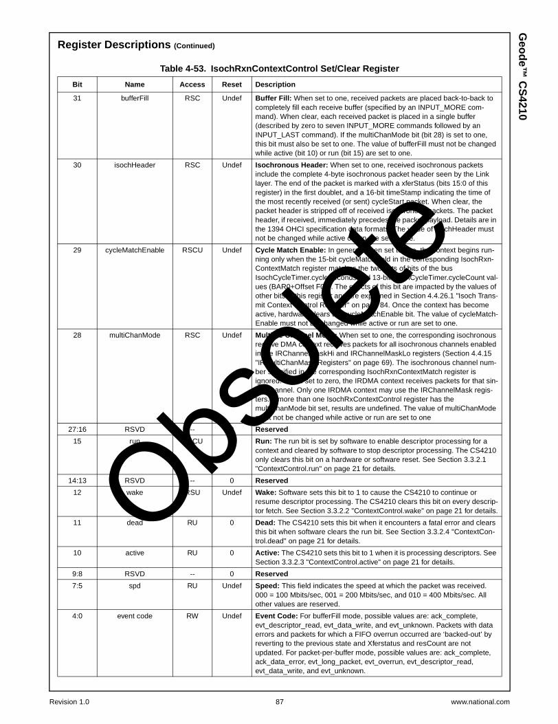
Revision 1.0 87 www.national.com
Geo
de™
CS
4210Register Descriptions (Continued)
Table 4-53. IsochRxnContextControl Set/Clear Register
Bit Name Access Reset Description
31 bufferFill RSC Undef Buffer Fill: When set to one, received packets are placed back-to-back tocompletely fill each receive buffer (specified by an INPUT_MORE com-mand). When clear, each received packet is placed in a single buffer(described by zero to seven INPUT_MORE commands followed by anINPUT_LAST command). If the multiChanMode bit (bit 28) is set to one,this bit must also be set to one. The value of bufferFill must not be changedwhile active (bit 10) or run (bit 15) are set to one.
30 isochHeader RSC Undef Isochronous Header: When set to one, received isochronous packetsinclude the complete 4-byte isochronous packet header seen by the Linklayer. The end of the packet is marked with a xferStatus (bits 15:0 of thisregister) in the first doublet, and a 16-bit timeStamp indicating the time ofthe most recently received (or sent) cycleStart packet. When clear, thepacket header is stripped off of received isochronous packets. The packetheader, if received, immediately precedes the packet payload. Details are inthe 1394 OHCI specification data formats. The value of isochHeader mustnot be changed while active or run are set to one.
29 cycleMatchEnable RSCU Undef Cycle Match Enable: In general, when set to one, the context begins run-ning only when the 15-bit cycleMatch field in the corresponding IsochRxn-ContextMatch register matches the two sets of bits of the busIsochCycleTimer.cycleSeconds and 13-bit IsochCycleTimer.cycleCount val-ues (BAR0+Offset F0h). The effects of this bit are impacted by the values ofother bits in this register and are explained in Section 4.4.26.1 "Isoch Trans-mit Context Control Register" on page 84. Once the context has becomeactive, hardware clears the cycleMatchEnable bit. The value of cycleMatch-Enable must not be changed while active or run are set to one.
28 multiChanMode RSC Undef Multiple Channel Mode: When set to one, the corresponding isochronousreceive DMA context receives packets for all isochronous channels enabledin the IRChannelMaskHi and IRChannelMaskLo registers (Section 4.4.15"IRMultiChanMask Registers" on page 69). The isochronous channel num-ber specified in the corresponding IsochRxnContextMatch register isignored. When set to zero, the IRDMA context receives packets for that sin-gle channel. Only one IRDMA context may use the IRChannelMask regis-ters. If more than one IsochRxContextControl register has themultiChanMode bit set, results are undefined. The value of multiChanModemust not be changed while active or run are set to one
27:16 RSVD -- 0 Reserved
15 run RSCU 0 Run: The run bit is set by software to enable descriptor processing for acontext and cleared by software to stop descriptor processing. The CS4210only clears this bit on a hardware or software reset. See Section 3.3.2.1"ContextControl.run" on page 21 for details.
14:13 RSVD -- 0 Reserved
12 wake RSU Undef Wake: Software sets this bit to 1 to cause the CS4210 to continue orresume descriptor processing. The CS4210 clears this bit on every descrip-tor fetch. See Section 3.3.2.2 "ContextControl.wake" on page 21 for details.
11 dead RU 0 Dead: The CS4210 sets this bit when it encounters a fatal error and clearsthis bit when software clears the run bit. See Section 3.3.2.4 "ContextCon-trol.dead" on page 21 for details.
10 active RU 0 Active: The CS4210 sets this bit to 1 when it is processing descriptors. SeeSection 3.3.2.3 "ContextControl.active" on page 21 for details.
9:8 RSVD -- 0 Reserved
7:5 spd RU Undef Speed: This field indicates the speed at which the packet was received.000 = 100 Mbits/sec, 001 = 200 Mbits/sec, and 010 = 400 Mbits/sec. Allother values are reserved.
4:0 event code RW Undef Event Code: For bufferFill mode, possible values are: ack_complete,evt_descriptor_read, evt_data_write, and evt_unknown. Packets with dataerrors and packets for which a FIFO overrun occurred are ‘backed-out’ byreverting to the previous state and Xferstatus and resCount are notupdated. For packet-per-buffer mode, possible values are: ack_complete,ack_data_error, evt_long_packet, evt_overrun, evt_descriptor_read,evt_data_write, and evt_unknown.
Obsole
te

www.national.com 88 Revision 1.0
Geo
de™
CS
4210 Register Descriptions (Continued)
4.4.27.2 Isoch Receive Command Pointer RegisterThe CommandPtr register (Table 4-54) specifies theaddress of the context program which is executed when aDMA context is started. All descriptors are 16-byte aligned,so the four least-significant bits of any descriptor addressmust be zero. The four least-significant bits of the Com-mand Pointer register are used to encode a Z value thatindicates how many physically contiguous descriptors arepointed to by descriptorAddress. In buffer-fill mode, Z iseither one or zero. In packet-per-buffer mode, Z is fromzero to eight.
These registers are repeated at offsets of 20h times thecontext number (see Table 4-52 for offset address assign-ment).
4.4.27.3 Isoch Receive Context Match RegisterThe ContextMatch register (Table 4-55) is used to start acontext running on a specified cycle number, to filter incom-ing isochronous packets based on tag values and to waitfor packets with a specified sync value. All packets arechecked for a matching tag value, and a compare on syncis only performed when the descriptor’s w field is set to 11.See 1394 OHCI spec data fields for proper usage of the wfield. This register should only be written when Context-Control.active is 0, otherwise unspecified behavior results.
These registers are repeated at offsets of 20h times thecontext number (see Table 4-52 for offset address assign-ment).
Table 4-54. IsochRxnCommandPtr Register
Bit Name Access Reset Description
31:4 descriptorAddress RWU Undef Descriptor Address: Contains the upper 28 bits of the address of a 16-byte aligned descriptor block. See Section 3.3.2.5 "CommandPtr" on page22 for details.
3:0 Z RWU Undef Z: Indicates the number of contiguous 16-byte aligned blocks at theaddress pointed to by descriptorAddress. If Z is 0, it indicates that thedescriptorAddress is not valid.
Table 4-55. IsochRxnContextMatch Register
Bit Name Access Reset Description
31 tag3 RW Undef Tag 3: If set, this context matches on isochronous receive packets with atag field of 11h.
30 tag2 RW Undef Tag 2: If set, this context matches on isochronous receive packets with atag field of 10h.
29 tag1 RW Undef Tag 1: If set, this context matches on isochronous receive packets with atag field of 01h.
28 tag0 RW Undef Tag 0: If set, this context matches on isochronous receive packets with atag field of 00h.
27 RSVD -- 0 Reserved
26:12 cycleMatch RW Undef Cycle Match: Contains a 15-bit value, corresponding to the low order twobits of cycleSeconds and the 13-bit cycleCount field in the cycleStartpacket. If cycleMatchEnable (bit 29 of corresponding IsochRxnContextCon-trol register) is set, then this IRDMA context becomes enabled for receiveswhen the two low order bits of the bus cycleTime.cycleSeconds andcycleTime.cycleCount (BAR0+Offset F0h) values equal the cycleMatchvalue.
11:8 sync RW Undef Synchronous: This field contains the 4-bit field which is compared to thesync field of each isochronous packet for this channel when the commanddescriptor’s w field is set to 11h.
7 RSVD -- 0 Reserved
6 tag1SynFilter RW Undef Tag 1 Synchronous Filter: If set and the contextMatch.tag1 bit is set, thenpackets with tag 01h shall only be accepted into the context if the two most-significant bits of the packet’s sync field are 00h. Packets with tag valuesother than 01h shall be filtered according to the tag0, tag2 and tag3 bitsabove with no additional restrictions.
If clear, this context matches on isochronous receive packets as specified inthe tag[0:3] bits above with no additional restrictions.
5:0 channelNum RW Undef Channel Number: This 6-bit field indicates the isochronous channel num-ber for which this IRDMA context accepts packets.
Obsole
te
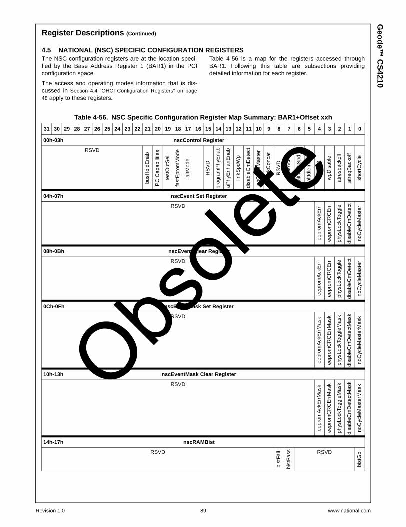
Revision 1.0 89 www.national.com
Geo
de™
CS
4210Register Descriptions (Continued)
4.5 NATIONAL (NSC) SPECIFIC CONFIGURATION REGISTERSThe NSC configuration registers are at the location speci-fied by the Base Address Register 1 (BAR1) in the PCIconfiguration space.
The access and operating modes information that is dis-cussed in Section 4.4 "OHCI Configuration Registers" on page48 apply to these registers.
Table 4-56 is a map for the registers accessed throughBAR1. Following this table are subsections providingdetailed information for each register.
Table 4-56. NSC Specific Configuration Register Map Summary: BAR1+Offset xxh
31 30 29 28 27 26 25 24 23 22 21 20 19 18 17 16 15 14 13 12 11 10 9 8 7 6 5 4 3 2 1 0
00h-03h nscControl Register
RSVDbu
sHol
dEna
b
PC
ICap
abili
ties
test
Out
Sel
fast
Epr
omM
ode
altM
ode
RS
VD
prog
ram
Phy
Ena
b
aPhy
Enh
anE
nab
linkS
pdW
p
disa
bleC
mD
etec
t
noC
ycle
Mas
ter
altA
ckC
onca
t
RS
VD
altA
ckA
ccel
altM
ultiS
pd
altId
leIn
sert
RS
VD
wpD
isab
le
atre
sbac
koff
atre
qBac
koff
shor
tCyc
le
04h-07h nscEvent Set Register
RSVD
eepr
omA
ckE
rr
eepr
omC
RC
Err
phys
Lock
Togg
le
disa
bleC
mD
etec
t
noC
ycle
Mas
ter
08h-0Bh nscEvent Clear Register
RSVD
eepr
omA
ckE
rr
eepr
omC
RC
Err
phys
Lock
Togg
le
disa
bleC
mD
etec
t
noC
ycle
Mas
ter
0Ch-0Fh nscEventMask Set Register
RSVDee
prom
Ack
Err
Mas
k
eepr
omC
RC
Err
Mas
k
phys
Lock
Togg
leM
ask
disa
bleC
mD
etec
tMas
k
noC
ycle
Mas
terM
ask
10h-13h nscEventMask Clear Register
RSVD
eepr
omA
ckE
rrM
ask
eepr
omC
RC
Err
Mas
k
phys
Lock
Togg
leM
ask
disa
bleC
mD
etec
tMas
k
noC
ycle
Mas
terM
ask
14h-17h nscRAMBist
RSVD
bist
Fail
bist
Pas
s RSVD
bist
Go
Obsole
te

www.national.com 90 Revision 1.0
Geo
de™
CS
4210 Register Descriptions (Continued)
18h-1Bh nscCmcControl
RSVD
CM
CL
CM
C
1Ch-1Fh Reserved
20h-23h nscTxThreshold
isochTxThrsh asyncTxThrsh
24h-27h nscSubSystem
deviceID vendorID
28h-3Fh Reserved
40h-43h nscPhysReadCount
RSVD physReadCount
44h-47h nscPhysWriteCount
RSVD physWriteCount
48h-4Bh nscPhysLockCount
RSVD physLockCount
4Ch-5Fh Reserved
60h-63h nscBusmgrID
busmgrID
64h-67h nscBandwAvail
bandwAvail
68h-6Bh nscChanAvailHi
chanAvailHi
6Ch-6Fh nscChanAvailLo
chanAvailLo
Table 4-56. NSC Specific Configuration Register Map Summary: BAR1+Offset xxh (Continued)
31 30 29 28 27 26 25 24 23 22 21 20 19 18 17 16 15 14 13 12 11 10 9 8 7 6 5 4 3 2 1 0
Obsole
te
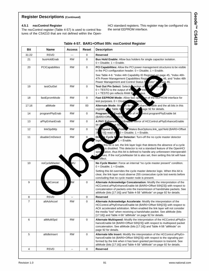
Revision 1.0 91 www.national.com
Geo
de™
CS
4210Register Descriptions (Continued)
4.5.1 nscControl RegisterThe nscControl register (Table 4-57) is used to control fea-tures of the CS4210 that are not defined within the Open-
HCI standard registers. This register may be configured viathe serial EEPROM interface.
Table 4-57. BAR1+Offset 00h: nscControl Register
Bit Name Access Reset Description
31:22 RSVD --- 0 Reserved
21 busHoldEnab RW 0 Bus Hold Enable: Allow bus holders for single capacitor isolation.0 = Disable; 1 = Enable.
20 PCICapabilities RW 0 PCI Capabilities: Allow the PCI power management structures to be visiblein the PCI configuration header. 0 = Disable; 1 = Enable.
See Table 4-6: "Index 44h Capability ID Register" on page 45, "Index 46h-47h Power Management Capabilities Register" on page 46, and "Index 48hPower Management and Control Status Register" on page 46.
19 testOutSel RW 0 Test Out Pin Select: Selects function of TESTO pin (pin 7).0 = TESTO is the output of the NAND tree.1 = TESTO pin reflects RAM BIST status.
18 fastEpromMode RW 0 Fast EEPROM Mode: Allow fast operation of the EEPROM interface fortest purposes. 0 = Disable; 1 = Enable.
17:16 altMode RW 00 Alternate Mode: Modifier for aPhyEnhanceEnable and the alt bits in thisregister. See Table 4-58 "altMode" on page 92 for details.
14 programPhyEnab RW 0 Program PHY Enable: Mirror of HCControl.programPhyEnable bit(BAR0+Offset 50h[23]).
13 aPhyEnhanEnab RW 0 A PHY Enhancement Enable: Mirror of HCControl.aPhyEnhanceEnablebit (BAR0+Offset 50h[22]).
12 linkSpdWp RW 0 Link Speed Write Protect: Makes BusOptions.link_spd field (BAR0+Offset20h[2:0]) read only. 0 = Disable; 1 = Enable.
11 disableCmDetect RW 0 Disable Cycle Master Detector: Turn-off the no cycle master detectorlogic. 0 = Disable; 1 = Enable.
When this bit is set, the link layer logic that detects the absence of a cyclemaster is disabled. This detector is not a standard feature of the OpenHCIspecification, thus this bit is defined to handle any unforeseen interoperabil-ity issues. If the noCycleMaster bit is also set, then setting this bit will haveno effect.
10 noCycleMaster RWU 0 No Cycle Master: Force an internal “no cycle master present” condition.0 = Disable; 1 = Enable.
Setting this bit overrides the cycle master detector logic. When this bit isclear, the link layer must observe 255 consecutive cycle lost events beforeconcluding that no cycle master node is present.
9 altAckConcat RW 0 Alternate Acknowledge Concatenation: Modify the interpretation of theHCControl.aPhyEnhanceEnable bit (BAR0+Offset 50h[23]) with respect toconcatenation of packets onto the transmission of handshake packets. SeealtMode (bits [17:16]) and Table 4-58 "altMode" on page 92 for details.
8 RSVD -- 0 Reserved
7 altAckAccel RW 0 Alternate Acknowledge Accelerate: Modify the interpretation of theHCControl.aPhyEnhanceEnable bit (BAR0+Offset 50h[23]) with respect toACK accelerated arbitration. When enabled the link layer will not considerthe media “lost” when receiving a handshake packet. See altMode (bits[17:16]) and Table 4-58 "altMode" on page 92 for details.
6 altMultiSpd RW 0 Alternate Multispeed: Modify the interpretation of the HCControl.aPhyEn-hanceEnable bit (BAR0+Offset 50h[23]) with respect to multispeed packetconcatenation. See altMode (bits [17:16]) and Table 4-58 "altMode" onpage 92 for details.
5 altIdleInsert RW 0 Alternate Idle Insert: Modify the interpretation of the HCControl.aPhyEn-hanceEnable bit (BAR0+Offset 50h[23]) with respect to the signaling per-formed by the link when it has been granted permission to transmit. SeealtMode (bits [17:16]) and Table 4-58 "altMode" on page 92 for details.
4 RSVD -- 0 Reserved
Obsole
te
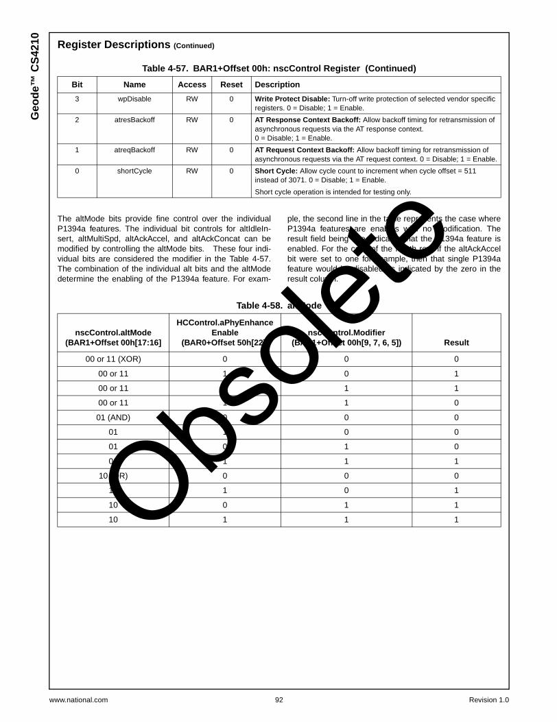
www.national.com 92 Revision 1.0
Geo
de™
CS
4210 Register Descriptions (Continued)
The altMode bits provide fine control over the individualP1394a features. The individual bit controls for altIdleIn-sert, altMultiSpd, altAckAccel, and altAckConcat can bemodified by controlling the altMode bits. These four indi-vidual bits are considered the modifier in the Table 4-57.The combination of the individual alt bits and the altModedetermine the enabling of the P1394a feature. For exam-
ple, the second line in the table represents the case whereP1394a features are enables with no modification. Theresult field being one indicates that the P1394a feature isenabled. For the case of the fourth row, if the altAckAccelbit were set to one for example, then that single P1394afeature would be disabled as indicated by the zero in theresult column.
3 wpDisable RW 0 Write Protect Disable: Turn-off write protection of selected vendor specificregisters. 0 = Disable; 1 = Enable.
2 atresBackoff RW 0 AT Response Context Backoff: Allow backoff timing for retransmission ofasynchronous requests via the AT response context.0 = Disable; 1 = Enable.
1 atreqBackoff RW 0 AT Request Context Backoff: Allow backoff timing for retransmission ofasynchronous requests via the AT request context. 0 = Disable; 1 = Enable.
0 shortCycle RW 0 Short Cycle: Allow cycle count to increment when cycle offset = 511instead of 3071. 0 = Disable; 1 = Enable.
Short cycle operation is intended for testing only.
Table 4-57. BAR1+Offset 00h: nscControl Register (Continued)
Bit Name Access Reset Description
Table 4-58. altMode
nscControl.altMode(BAR1+Offset 00h[17:16]
HCControl.aPhyEnhanceEnable
(BAR0+Offset 50h[22])nscControl.Modifier
(BAR1+Offset 00h[9, 7, 6, 5]) Result
00 or 11 (XOR) 0 0 0
00 or 11 1 0 1
00 or 11 0 1 1
00 or 11 1 1 0
01 (AND) 0 0 0
01 1 0 0
01 0 1 0
01 1 1 1
10 (OR) 0 0 0
10 1 0 1
10 0 1 1
10 1 1 1Obsole
te

Revision 1.0 93 www.national.com
Geo
de™
CS
4210Register Descriptions (Continued)
4.5.2 nscEventSet/ClearThe nscEvent register (Table 4-59) contains events that areunique to the CS4210. This register is set (BAR1+Offset04h) and clear (BAR1+Offset 08h).
4.5.3 nscMaskSet/ClearThe nscEventMask register (Table 4-60) controls themasking of the nscEvent register. This register is set(BAR1+Offset 0Ch) and clear (BAR1+Offset 10h).
Table 4-59. BAR1+Offset 04h (Set) and 08h (Clear): nscEvent Register
Bit Name Access Reset Description
31:5 RSVD -- 0 Reserved
4 eepromAckErr RSCU Undef EEPROM Acknowledge Error: Set when an acknowledge is missing fromthe serial EEPROM load.
3 eepromCRCErr RSCU Undef EEPROM Cyclical Redundancy Check Error: Set when a CRC erroroccurs as a result of the serial EEPROM load.
2 physLockToggle RSCU Undef Physical Lock Toggle: Set when D15 of the nscPhysLockCount register(BAR1+Offset 48h) changes.
1 disableCmDetect RSCU Undef Disable Cycle Master Detector: Set when D15 of the nscPhysWriteCountregister (BAR1+Offset 44h) changes.
0 noCycleMaster RSCU Undef No Cycle Master: Set when D15 of the nscPhysReadCount register(BAR1+Offset 40h) changes.
Table 4-60. BAR1+Offset 0Ch (Set) and 10h (Clear): nscEventMask Register
Bit Name Access Reset Description
31:5 RSVD -- 0 Reserved
4 eepromAckErrMask RSCU Undef EEPROM Acknowledge Error Mask: Set to 1 enables the corresponding bitin the nscEvent register (BAR1+Offset 04h).
3 eepromCRCErrMask RSC Undef EEPROM Cyclical Redundancy Check Error Mask: Set to 1 enables thecorresponding bit in the nscEvent register (BAR1+Offset 04h).
2 physLockToggleMask RSC Undef Physical Lock Toggle Mask: Set to 1 enables the corresponding bit in thenscEvent register (BAR1+Offset 04h).
1 disableCmDetectMask RSC Undef Disable Cycle Master Detector Mask: Set to 1 enables the correspondingbit in the nscEvent register (BAR1+Offset 04h).
0 noCycleMasterMask RSC Undef No Cycle Master Mask: Set to 1 enables the corresponding bit in thenscEvent register (BAR1+Offset 04h).
Obsole
te

www.national.com 94 Revision 1.0
Geo
de™
CS
4210 Register Descriptions (Continued)
4.5.4 nscRAMBistThe nscRAMBist register (Table 4-61) is used to test theFIFOs implemented in SRAM. The bistGo bit is set and thebistFail and bistPass bits are polled until one is set, indicat-ing pass or fail. The CS4210 must be reset before normaloperation can resume.
4.5.5 nscCmcControlThe nscCmcControl register (Table 4-62) controls the stateof the CMC and CMCL pins. These pins are intended foruse with Contender pins on 1394-1995 PHY devices. Thisfeature is not used on the CS4103.
4.5.6 nscTxThresholdThe nscTxThreshold register (Table 4-63) is used to controlthe point at which the transmit FIFOs start sending data
over the 1394 bus. Lowering the threshold value causessmaller packets to be sent. This register can only be writtento when the nscControl.wpDisable bit (BAR1+Offset00h[3]) is set. This register may be configured via the serialEEPROM interface (if EEPROM is present).
4.5.7 nscSubSystemThe nscSubSystem register (Table 4-64) is used to config-ure the subsystem vendor ID and the subsystem device IDvalues in the PCI configuration space. This register canonly be written to when the nscControl.wpDisable bit(BAR1+Offset 00h[3]) is set. This register may be config-ured via the serial EEPROM interface (if EEPROM ispresent).
.
Table 4-61. BAR1+Offset 14h: nscRAMBist Register
Bit Name Access Reset Description
31:10 RSVD -- 0 Reserved
9 bistFail RU Undef Built-in Self-Test Fail: Set to 1 when RAM BIST has failed.
8 bistPass RU Undef Built-in Self-Test Pass: Set to 1 when RAM BIST has passed.
7:1 RSVD -- 0 Reserved
0 bistGo RW Undef Built-in Self-Test Go: RAM BIST is started by writing a 1 to this bit.
Table 4-62. BAR1+Offset 18h: nscCmcControl Register
Bit Name Access Reset Description
31:2 RSVD -- 0 Reserved
1 CMCL RW 0 Contender Master Control Link Enabled: This bit is ANDed with HCCon-trol.LinkEnable (BAR0+Offset 50h[17]) and the result is reflected on pin 3.
0 CMC RW 0 Contender Master Control: Selects polarity of CMC output. This bit isdirectly reflected on pin 2. 0 = Low; 1 = High.
Table 4-63. BAR1+Offset 20h: nscTxThreshold Register
Bit Name Access Reset Description
31:16 isochTxThrsh RW 01FEh Isochronous Transmit Threshold: FIFO threshold value when transmit-ting isochronous packets. D[18:16] are hardwired to 110 and D[31:25] arehardwired to 00h.
15:0 asyncTxThrsh RU 01FEh Asynchronous Transmit Threshold: FIFO threshold value when transmit-ting asynchronous packets. D[2:0] are hardwired to 110 and the D[15:9] arehardwired to 00h.
Table 4-64. BAR1+Offset 24h: nscSubSystem Register
Bit Name Access Reset Description
31:16 deviceID RW 0000h Device ID: PCI configuration subsystem device ID.
15:0 vendorID RW 0000h Vendor ID: PCI configuration subsystem vendor ID.
Obsole
te

Revision 1.0 95 www.national.com
Geo
de™
CS
4210Register Descriptions (Continued)
4.5.8 nscPhysReadCountThe nscPhysReadCount register (Table 4-65) provides sta-tistics on physical read requests and CSR read requests.This register is cleared when a 1 is written to D0.
4.5.9 nscPhysWriteCountThe nscPhysWriteCount register (Table 4-66) provides sta-tistics on physical write requests. This register is clearedwhen a 1 is written to D0.
4.5.10 nscPhysLockCountThe nscPhysLockCount register (Table 4-67) provides sta-tistics on physical lock requests. This register is clearedwhen a 1 is written to D0.
Table 4-65. BAR1+Offset 40h: nscPhysReadCount
Bit Name Access Reset Description
31:16 RSVD -- 0 Reserved
15:0 physReadCount RW 0000h Physical Read Count: Current count of physical read requests and/or CSRread requests.
Table 4-66. BAR1+Offset 44h: nscPhysWriteCount Register
Bit Name Access Reset Description
31:16 RSVD -- 0 Reserved
15:0 physWriteCount RW 0000h Physical Write Count: Current count of physical write requests.
Table 4-67. BAR1+Offset 48h: nscPhysLockCount Register
Bit Name Access Reset Description
31:16 RSVD -- 0 Reserved
15:0 physLockCount RW 0000h Physical Lock Count: Current count of physical lock requests.
Obsole
te

www.national.com 96 Revision 1.0
Geo
de™
CS
4210 Register Descriptions (Continued)
4.5.11 nscBusmgrIDThe nscBusmgrID register (Table 4-68) is a directly read-able BUS_MANAGER_ID CSR resource.
4.5.12 nscBandwAvailThe nscBandwAvail register (Table 4-69) is a directly read-able BANDWIDTH_AVAILABLE CSR resource.
4.5.13 nscChanAvailHiThe nscChanAvailHi register (Table 4-70) is a directly read-able CHANNELS_AVAILALBLE_HI CSR resource.
4.5.14 nscChanAvailLoThe nscChanAvailLo register (Table 4-71) is a directly read-able CHANNELS_AVAILABLE_LO CSR resource.
Table 4-68. BAR1+Offset 60h: nscBusmgrID Register
Bit Name Access Reset Description
31:0 busmgrID R Undef Bus Manager ID: BUS_MANAGER_ID CSR resource.
Table 4-69. BAR1+Offset 64h: nscBandwAvail Register
Bit Name Access Reset Description
31:0 bandwAvail R Undef Bandwidth Available: BANDWIDTH_AVAILABLE CSR resource.
Table 4-70. BAR1+Offset 68h: nscChanAvailHi Register
Bit Name Access Reset Description
31:0 chanAvailHi R Undef Channels Available High: CHANNELS_AVAILALBLE_HI CSR resource.
Table 4-71. BAR1+Offset 6Ch: nscChanAvailLo Register
Bits Field Name Access Reset Description
31:0 chanAvailLo R Undef Channels Available Low: CHANNELS_AVAILALBLE_LO CSR resource.
Obsole
te

Revision 1.0 97 www.national.com
Geo
de™
CS
42105.0 Electrical SpecificationsThis section provides information on NAND tree test mode,absolute maximum ratings, recommended operating condi-tions, and DC/AC characteristics for the Geode CS4210.
5.1 NAND TREE TEST MODEThe NAND tree test mode is used to test input and bidirec-tional pins which are part of the NAND tree chain. Afterpower is applied to the CS4210, pin 7 (TESTO) is the out-put of the NAND tree. To test the NAND tree, all inputs inTable 5-1 are held low and then a high is successively
applied to the inputs in the order listed in Table 5-1. TheTESTO output will toggle on each input change as shownin Figure 5-1.
The TESTO pin will continue to output the result of theNAND tree during normal operation. If this is undesirable,nscControl.testOutSel (BAR1+Offset 00h[19]) can be setand TESTO will reflect the BIST output which does not tog-gle during normal operation. The nscControl register isloaded via the serial EEPROM upon power up, so nscCon-trol.testOutSel can be set as the default if desired.
Table 5-1. NAND Tree Test Mode Pins
Signal Name Pin No.
LNKON 98
SCLK 95
CTL0 93
CTL1 92
DATA0 90
DATA1 89
DATA2 88
DATA3 86
DATA4 85
DATA5 84
DATA6 82
DATA7 81
DIRECT 79
CCLKI 78
TESTEN# 76
AD0 74
AD1 73
AD2 72
AD3 71
AD4 69
AD5 68
AD6 67
AD7 66
C/BE0# 65
AD8 64
AD9 62
AD10 61
AD11 59
AD12 58
AD13 57
AD14 56
AD15 54
C/BE1# 53
PAR 52
Signal Name Pin No.
SERR# 51
PERR# 49
STOP# 48
DEVSEL# 47
TRDY# 45
IRDY# 44
FRAME# 43
C/BE2# 41
AD16 40
AD17 38
AD18 37
AD19 36
AD20 34
AD21 33
AD22 32
AD23 31
IDSEL 29
Signal Name Pin No.
C/BE3# 28
AD24 27
AD25 26
AD26 25
AD27 23
AD28 22
AD29 21
AD30 19
AD31 18
PME# 17
PGNT# 14
PCLK 12
RST# 10
EEDATA 5
EECLK 4
Signal Name Pin No.
Figure 5-1. NAND Tree Output Waveform
TESTO
LNKON
SCLK
CTL0
CTL1
DATA0
100 ns
:::::::::
EECLK
Note: The following pins are not in the NAND tree: CMC, CMCL, INTA#, PREQ#, CCLKO, LREQ, LPS, and all supplies.
Obsole
te

www.national.com 98 Revision 1.0
Geo
de™
CS
4210 Electrical Specifications (Continued)
5.2 ABSOLUTE MAXIMUM RATINGSTable 5-2 lists the absolute maximum ratings for theCS4210. Stresses beyond the listed ratings may causepermanent damage to the device. Exposure to conditionsbeyond these limits may (1) reduce device reliability and (2)result in premature failure even when there is no immedi-ately apparent sign of failure. Prolonged exposure to condi-tions at or near the absolute maximum ratings may alsoreduce useful life and reliability. These are stress ratings
only and do not imply that operation under any conditionsother than those listed in Table 5-3 is possible.
5.3 OPERATING CONDITIONSAll DC and AC parameters were measured under the oper-ating conditions listed in Table 5-3.
Table 5-2. Absolute Maximum Ratings
Parameter Units
Supply Voltage, VDD, VDDIO –0.5V to 3.75V
Input Voltage –0.5V to VDDIO + 1.7V
Output Voltage –0.5V to VDDIO + 0.5V
Storage Temperature, TSTG –65°C to 150°C
ESD Tolerance 2000V
Lead Temperature, TL 230°C (Soldering 10 seconds)
Table 5-3. Operating Conditions
Parameter Units
I/O Supply Voltage, VDDIO 3.0V to 3.6V
Supply Voltage, VDD 2.3V to 2.7V
Operating Temperature, TA 0°C to 70°C
Power Dissipation, PD 300 mW
Obsole
te

Revision 1.0 99 www.national.com
Geo
de™
CS
4210Electrical Specifications (Continued)
5.4 DC CHARACTERISTICS
Table 5-4. DC Characteristics: PCI Interface
Symbol Parameter Min Max Units Conditions
VDDIO I/O Supply Voltage 3.0 3.6 V
VDD Core Supply Voltage 2.3 2.7 V
VIH Input High Voltage 1.7 V
VIL Input Low Voltage –0.5 0.7 V
VIPU Input Pull-up Voltage 1.7 V
IIH Input High Leakage Current + 10 µA 0 < VIN < VDDIO
IIL Input Low Leakage Current –10 µA 0 < VIN < VDDIO
VOH1 Output High Voltage VDDIO–0.2 V IOUT = –10 µA
VOH2 Output High Voltage 2.4 V IOUT = –2 mA
VOL1 Output Low Voltage 0.2 V IOUT = 10 µA
VOL2 Output Low Voltage 0.4 V IOUT = 2 mA
CIN Input Pin Capacitance 10 pF
CCLK CLK Pin Capacitance 5 12 pF
CIDSEL IDSEL Pin Capacitance 8 pF
LPIN Pin Inductance 20 nH
Table 5-5. DC Characteristics: General
Symbol Parameter Min Typ Max Units Conditions
VDDIO I/O Supply Voltage 3.0 3.6 V
VDD Core Supply Voltage 2.3 2.7 V
IDDQ Quiescent Core Supply Current 100 µA
IDDQIO Quiescent I/O Supply Current 500 µA
IDD Dynamic Core Supply Current 80 mA
IDDIO Dynamic Supply Current 13 mAObsole
te

www.national.com 100 Revision 1.0
Geo
de™
CS
4210 Electrical Specifications (Continued)
Table 5-6. IEEE 1394a PHY-Link Interface
Symbol Parameter Min Max Units Conditions
VDDIO Supply Voltage 3.0 3.6 V
VDD Core Supply Voltage 2.3 2.7 V
VIH Input High Voltage 2.8 VDD+10% V
VIL Input Low Voltage GND 0.7 V
IIH Input High Leakage Current 40 µA
IIL Input Low Leakage Current 600 µA
VOH Output High Voltage 2.8 VDD V IOUT = –4 mA
VOL Output Low Voltage GND 0.4 V IOUT = 4 mA
CIN Input Pin Capacitance 7.5 pF
Obsole
te

Revision 1.0 101 www.national.com
Geo
de™
CS
4210Electrical Specifications (Continued)
5.5 AC SPECIFICATIONS
Figure 5-2. PCI Timing Waveform
Figure 5-3. PCI Setup and Hold Timing
Table 5-7. PCI Timings: CLOAD = 50 pF
Symbol Parameter Min Max Units
tVAL CLK to Signal Valid Delay - bused signals 2 11 ns
tON Float to Active Delay 2 ns
tOFF Active to Float Delay 28 ns
tSU Input Setup Time to CLK - bused signals 7 ns
tH Input Hold Time from CLK 0 ns
tRST Reset Active Time after Power Stable 1 ms
tRST-CLK Reset Active Time after CLK Stable 100 ms
tRST-OFF Reset Active Time to Output TRI-STATE Delay 40 ns
tCYC PCLK Cycle Time 30 ns
tHIGH PCLK High Time 11 ns
tLOW PCLK Low Time 11 ns
PCLK
PCI
TRI-STATEOutput
tVAL
tONtOFF
Output
PCLK
PCI
tH
tSU
Output
Obsole
te
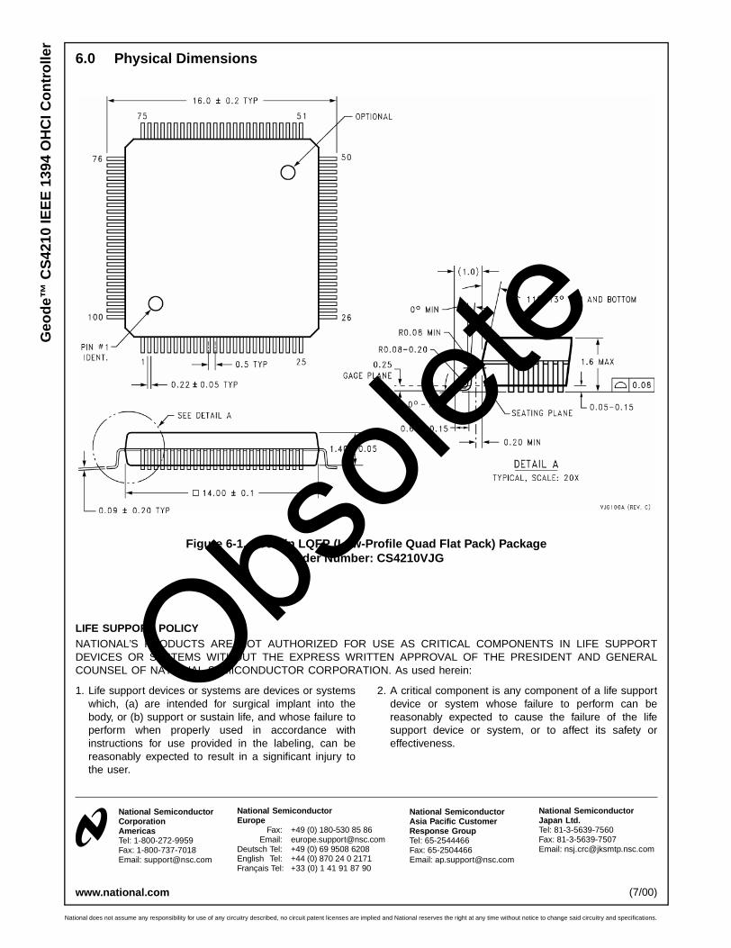
Geo
de™
CS
4210
IEE
E13
94O
HC
ICo
ntr
olle
r
National does not assume any responsibility for use of any circuitry described, no circuit patent licenses are implied and National reserves the right at any time without notice to change said circuitry and specifications.
www.national.com (7/00)
National SemiconductorCorporationAmericasTel: 1-800-272-9959Fax: 1-800-737-7018Email: [email protected]
National SemiconductorEurope
Fax: +49 (0) 180-530 85 86Email: [email protected]
Deutsch Tel: +49 (0) 69 9508 6208English Tel: +44 (0) 870 24 0 2171Français Tel: +33 (0) 1 41 91 87 90
National SemiconductorAsia Pacific CustomerResponse GroupTel: 65-2544466Fax: 65-2504466Email: [email protected]
National SemiconductorJapan Ltd.Tel: 81-3-5639-7560Fax: 81-3-5639-7507Email: [email protected]
LIFE SUPPORT POLICYNATIONAL’S PRODUCTS ARE NOT AUTHORIZED FOR USE AS CRITICAL COMPONENTS IN LIFE SUPPORTDEVICES OR SYSTEMS WITHOUT THE EXPRESS WRITTEN APPROVAL OF THE PRESIDENT AND GENERALCOUNSEL OF NATIONAL SEMICONDUCTOR CORPORATION. As used herein:
1. Life support devices or systems are devices or systemswhich, (a) are intended for surgical implant into thebody, or (b) support or sustain life, and whose failure toperform when properly used in accordance withinstructions for use provided in the labeling, can bereasonably expected to result in a significant injury tothe user.
2. A critical component is any component of a life supportdevice or system whose failure to perform can bereasonably expected to cause the failure of the lifesupport device or system, or to affect its safety oreffectiveness.
6.0 Physical Dimensions
Figure 6-1. 100-Pin LQFP (Low-Profile Quad Flat Pack) PackageOrder Number: CS4210VJG
Obsole
te

IMPORTANT NOTICE
Texas Instruments Incorporated and its subsidiaries (TI) reserve the right to make corrections, modifications, enhancements, improvements,and other changes to its products and services at any time and to discontinue any product or service without notice. Customers shouldobtain the latest relevant information before placing orders and should verify that such information is current and complete. All products aresold subject to TI’s terms and conditions of sale supplied at the time of order acknowledgment.
TI warrants performance of its hardware products to the specifications applicable at the time of sale in accordance with TI’s standardwarranty. Testing and other quality control techniques are used to the extent TI deems necessary to support this warranty. Except wheremandated by government requirements, testing of all parameters of each product is not necessarily performed.
TI assumes no liability for applications assistance or customer product design. Customers are responsible for their products andapplications using TI components. To minimize the risks associated with customer products and applications, customers should provideadequate design and operating safeguards.
TI does not warrant or represent that any license, either express or implied, is granted under any TI patent right, copyright, mask work right,or other TI intellectual property right relating to any combination, machine, or process in which TI products or services are used. Informationpublished by TI regarding third-party products or services does not constitute a license from TI to use such products or services or awarranty or endorsement thereof. Use of such information may require a license from a third party under the patents or other intellectualproperty of the third party, or a license from TI under the patents or other intellectual property of TI.
Reproduction of TI information in TI data books or data sheets is permissible only if reproduction is without alteration and is accompaniedby all associated warranties, conditions, limitations, and notices. Reproduction of this information with alteration is an unfair and deceptivebusiness practice. TI is not responsible or liable for such altered documentation. Information of third parties may be subject to additionalrestrictions.
Resale of TI products or services with statements different from or beyond the parameters stated by TI for that product or service voids allexpress and any implied warranties for the associated TI product or service and is an unfair and deceptive business practice. TI is notresponsible or liable for any such statements.
TI products are not authorized for use in safety-critical applications (such as life support) where a failure of the TI product would reasonablybe expected to cause severe personal injury or death, unless officers of the parties have executed an agreement specifically governingsuch use. Buyers represent that they have all necessary expertise in the safety and regulatory ramifications of their applications, andacknowledge and agree that they are solely responsible for all legal, regulatory and safety-related requirements concerning their productsand any use of TI products in such safety-critical applications, notwithstanding any applications-related information or support that may beprovided by TI. Further, Buyers must fully indemnify TI and its representatives against any damages arising out of the use of TI products insuch safety-critical applications.
TI products are neither designed nor intended for use in military/aerospace applications or environments unless the TI products arespecifically designated by TI as military-grade or "enhanced plastic." Only products designated by TI as military-grade meet militaryspecifications. Buyers acknowledge and agree that any such use of TI products which TI has not designated as military-grade is solely atthe Buyer's risk, and that they are solely responsible for compliance with all legal and regulatory requirements in connection with such use.
TI products are neither designed nor intended for use in automotive applications or environments unless the specific TI products aredesignated by TI as compliant with ISO/TS 16949 requirements. Buyers acknowledge and agree that, if they use any non-designatedproducts in automotive applications, TI will not be responsible for any failure to meet such requirements.
Following are URLs where you can obtain information on other Texas Instruments products and application solutions:
Products Applications
Audio www.ti.com/audio Communications and Telecom www.ti.com/communications
Amplifiers amplifier.ti.com Computers and Peripherals www.ti.com/computers
Data Converters dataconverter.ti.com Consumer Electronics www.ti.com/consumer-apps
DLP® Products www.dlp.com Energy and Lighting www.ti.com/energy
DSP dsp.ti.com Industrial www.ti.com/industrial
Clocks and Timers www.ti.com/clocks Medical www.ti.com/medical
Interface interface.ti.com Security www.ti.com/security
Logic logic.ti.com Space, Avionics and Defense www.ti.com/space-avionics-defense
Power Mgmt power.ti.com Transportation and Automotive www.ti.com/automotive
Microcontrollers microcontroller.ti.com Video and Imaging www.ti.com/video
RFID www.ti-rfid.com
OMAP Mobile Processors www.ti.com/omap
Wireless Connectivity www.ti.com/wirelessconnectivity
TI E2E Community Home Page e2e.ti.com
Mailing Address: Texas Instruments, Post Office Box 655303, Dallas, Texas 75265Copyright © 2011, Texas Instruments Incorporated


