micromachines Article Geometrical Representation of a Polarisation Management Component on a SOI Platform Massimo Valerio Preite 1 , Vito Sorianello 2 , Gabriele De Angelis 2 , Marco Romagnoli 2 and Philippe Velha 1, * 1 Scuola Superiore Sant’Anna—TeCIP Institute, Via Moruzzi 1, 56124 Pisa, Italy; [email protected]2 CNIT—Laboratory of Photonic Networks, Via Moruzzi 1, 56124 Pisa, Italy; [email protected] (V.S.); [email protected] (G.D.A.); [email protected] (M.R.) * Correspondence: [email protected]; Tel.: +39-050-88-2187 Received: 19 April 2019; Accepted: 26 May 2019; Published: 30 May 2019 Abstract: Grating couplers, widely used in Silicon Photonics (SiPho) for fibre-chip coupling are polarisation sensitive components, consequently any polarisation fluctuation from the fibre optical link results in spurious intensity swings. A polarisation management componentis analytically considered, coupled with a geometrical representation based on phasors and Poincaré sphere, generalising and simplifying the treatment and understanding of its functionalities. A specific implementation in SOI is shown both as polarisation compensator and polarisation controller, focusing on the operative principle. Finally, it is demonstrated experimentally that this component can be used as an integrated polarimeter. Keywords: Silicon Photonics; off-chip coupling; polarisation controller; integrated polarimeter; polarisation multiplexing; polarisation shift keying 1. Introduction Silicon photonics, thanks to its compatibility with CMOS technology, is imposing itself for large scale fabrication of low cost and small footprint photonic integrated circuits (PICs). One of Silicon Photonics main challenges is coupling light in and out from the chip in an efficient and practical way. The high index contrast between silicon and silica enables the use of grating couplers (GC), that, to our knowledge, are the most widespread off chip coupling solution, mainly thanks to the design flexibility deriving from the fact that they can be placed nearly everywhere on the chip and are not constrained to the chip edge. An important limitation of GCs is their polarisation sensitivity; consequently, the input polarisation fluctuations that regularly occur in optical fibres as a result of deformations or temperature changes translate into random spurious amplitude modulations. Other coupling schemes, such as butt or end fire coupling, are possible, but they are not of interest for this paper. The problem of assuring polarisation tracking was broadly addressed decades ago, as it is critical for the working of coherent optical systems, given the need to match the time varying State of Polarisation (SOP) of the input signal to the local oscillator’s one. The proposed solutions were based on fibre squeezers [1], lithium-niobate integrated devices [2,3] and Planar Lightwave Circuit (PLC) technology [4]. In [5], the proof of concept of Caspers et al. [6] was further developed into a fully functional building block with two independent phase shifters and was integrated at the two ends of the bus waveguide in a subsystem presented in [7] , thus making it transparent to polarisation fluctuations. Until now, the strategy to cope with polarisation fluctuations has been to separate the signal in two orthogonal polarisations and duplicate the circuits , in what is called polarisation diversity scheme. Micromachines 2019, 10, 364; doi:10.3390/mi10060364 www.mdpi.com/journal/micromachines
Transcript
micromachines
Article
Geometrical Representation of a PolarisationManagement Component on a SOI Platform
Massimo Valerio Preite 1 , Vito Sorianello 2, Gabriele De Angelis 2, Marco Romagnoli 2
and Philippe Velha 1,*1 Scuola Superiore Sant’Anna—TeCIP Institute, Via Moruzzi 1, 56124 Pisa, Italy; [email protected] CNIT—Laboratory of Photonic Networks, Via Moruzzi 1, 56124 Pisa, Italy; [email protected] (V.S.);
Received: 19 April 2019; Accepted: 26 May 2019; Published: 30 May 2019
Abstract: Grating couplers, widely used in Silicon Photonics (SiPho) for fibre-chip coupling arepolarisation sensitive components, consequently any polarisation fluctuation from the fibre opticallink results in spurious intensity swings. A polarisation management componentis analyticallyconsidered, coupled with a geometrical representation based on phasors and Poincaré sphere,generalising and simplifying the treatment and understanding of its functionalities. A specificimplementation in SOI is shown both as polarisation compensator and polarisation controller,focusing on the operative principle. Finally, it is demonstrated experimentally that this componentcan be used as an integrated polarimeter.
Silicon photonics, thanks to its compatibility with CMOS technology, is imposing itself for largescale fabrication of low cost and small footprint photonic integrated circuits (PICs). One of SiliconPhotonics main challenges is coupling light in and out from the chip in an efficient and practical way.The high index contrast between silicon and silica enables the use of grating couplers (GC), that, to ourknowledge, are the most widespread off chip coupling solution, mainly thanks to the design flexibilityderiving from the fact that they can be placed nearly everywhere on the chip and are not constrained tothe chip edge. An important limitation of GCs is their polarisation sensitivity; consequently, the inputpolarisation fluctuations that regularly occur in optical fibres as a result of deformations or temperaturechanges translate into random spurious amplitude modulations. Other coupling schemes, such as buttor end fire coupling, are possible, but they are not of interest for this paper.
The problem of assuring polarisation tracking was broadly addressed decades ago, as it is criticalfor the working of coherent optical systems, given the need to match the time varying State ofPolarisation (SOP) of the input signal to the local oscillator’s one. The proposed solutions were basedon fibre squeezers [1], lithium-niobate integrated devices [2,3] and Planar Lightwave Circuit (PLC)technology [4].
In [5], the proof of concept of Caspers et al. [6] was further developed into a fully functionalbuilding block with two independent phase shifters and was integrated at the two ends of the buswaveguide in a subsystem presented in [7] , thus making it transparent to polarisation fluctuations.Until now, the strategy to cope with polarisation fluctuations has been to separate the signal in twoorthogonal polarisations and duplicate the circuits , in what is called polarisation diversity scheme.
In this example, the compensator is able to convert any SOP into the standard TE mode of SiliconPhotonics waveguide eluding a duplicated circuit.
The current article extends the results in [5,6], and aims at developing a simple but precise andexhaustive geometrical picture based on both phasor and Bloch sphere representation. The use of thispictorial representation is illustrated by solving the problem of the frequency response together withits effect on the point representing the SOP on the Poincaré sphere.
In polarisation tracking, sometimes it is not enough to have a device that can compensate allpossible SOPs, but it may be desirable to have an endless system, i.e., one where resets—when thephysical quantity producing the phase shift reaches any end of its range and a phase jump of aninteger number of 2π must be applied—are collision-free and do not provoke transmission disruptionsnor information losses. Even better is a reset-free system, that is, one in which potentially unlimitedphase shifts can be achieved with the control quantity limited in a finite interval. Usual wave platetransformers possess this last property [2] and have been implemented in lithium-niobate [8,9] .Quarter- and half-wave plates can be implemented in PLC [10], thus even in SiPho. Hence, the samefunctionality of the device in [2] can be achieved in SiPho, at the price of a greater complexity.
This paper is organised in the following way: after a short description of the device structure inSection 1.1, Section 2 analyses single wavelength operation, while Section 3 examines the frequencyresponse. In both cases, both operating modes are analysed: here “compensator” refers to the casein which the light enters from the 2DGC and the circuit acts so that all the power is routed towardone of its two ends, while “controller” means the reciprocal case where the input is one of the twowaveguides and the device settings determine the polarisation exiting from the 2DGC.
In Section 2.1, a phasor representation illustrates the particular case of the polarisationcompensation. Two classes of periodical solutions are found, for any input SOP. As a corollary,the knowledge of the phase shifts needed to compensate the input of an unknown SOP can be used tomeasure without ambiguity this SOP. For the first time, it is demonstrated that a polarimeter can bemade in a silicon photonics platform.
Next, several properties are derived thanks to the graphical representation as a function of twophysical quantities: the applied phase shifts.
In Section 2.2, the operation as polarisation controller is examined, proving that all the SOPs canbe generated and the effect of the two phase shifters on the corresponding point on Poincaré sphereis described.
Section 3 examines the frequency response for both the compensator and the generator operation.Using the expression provided in [11] for the frequency and temperature dependence of SOI effectiveindex, an expression for the phase shift frequency dependence is derived. A transcendental implicitequation for the −3 dB bandwidth is found and it is shown that the frequency response is non trivialdepending in both the considered input SOP and the chosen phase shift pair. Then, those results aretransposed to Poincaré sphere.
Finally, Section 4 presents an experimental test of the derived results.
1.1. Device Schematic
The device exploits a 2D grating coupler (2DGC) to split the incoming field into two orthogonalcomponents. These two components are then fed into two distinct integrated waveguides.
The first stage introduces a first phase shift, then the fields in the two branches are combined andagain split by means of an MMI, and undergo another phase shift.
Eventually, a second MMI recombines the fields and sends its output to the two exits.In [7], the top output is terminated on a monitoring photodiode, while the bottom one is connected
to the rest of the PIC. The photodiode current is minimised during the module tuning to make surethat all the optical power goes to the bottom output and therefrom to the downhill PIC. For consistencywith that article and the work in [5], in the rest of this paper, we consider that only port “B” in Figure 1is used.
Micromachines 2019, 10, 364 3 of 32
However, that is not the only possible arrangement. On the contrary, each port can be connectedto a distinct photonic module, which processes the information encoded on the SOP orthogonal to thatof the other output, for instance in a POLarisation Shift Keying (POLSK) scheme.
φ1
L1
L2
T
2DGCMPS1 MC1
MPS2 MC2
φ2 B
Figure 1. Schematic of the integrated polarisation controller. The labels Mi refer to the transfer matrixassociated with a given circuit section. The block on the picture leftmost portion is a schematic of the2DGC. The “T” and “B” labels denote the top and bottom outputs, respectively.
2. Single Wavelength Operation
2.1. Compensator
The overall device, excluding the grating couplers, can be viewed as the cascade of four blocks;correspondingly, its total transfer matrix is the product of the four individual blocks matrices, whichare phase shifters (PS) and couplers (C), respectively, and read:
MPS =
[ei ∆ϕ 0
0 1
]MC =
cos(κ) −i sin(κ)
−i sin(κ) cos(κ)
=
1√2
[1 −i
−i 1
](1)
where ∆ϕ = ∆tb (βL) = ∆tb(β)L and the function ∆tb denotes the difference of the quantity betweenbrackets for the top and bottom arm. It is applied just to the propagation constant β as the two armsare ideally of equal length. The coupling coefficient is assumed to be κ = π/2 (3 dB coupler).
Thus, the overall transfer matrix reads:
T = MC2 MPS2 MC1 MPS1 =e−i ψ
2
ei φ1(1− ei φ2
)−i(1 + ei φ2
)
−i ei φ1(1 + ei φ2
)−(1− ei φ2
)
(2)
where ψ is an arbitrary absolute phase shift, and φ1 and φ2 are the applied phase shifts, as shownin Figure 1. As input, we consider a generic polarisation, described by the Jones vector in threeequivalent forms:
Ain = ei δ1
(a1
a2 ei δ
)= ei δ1
(cos α
sin α ei δ
)=
(q1
q2
)(3)
where q1 and q2 are defined as two complex values representing the input vector polarisation. The mainhypothesis of this works is that the 2DGC is supposed to split the TE and TM components withoutaffecting their relative amplitude and phases (attenuating or phase shifting them in the same way,i.e., without crosstalk), so that the input vector to the rest of the circuit can be assumed to coincidewith the above Jones vector.
Thus, the output complex amplitudes vector from the circuit is:
Aout =
(aup
abottom
)= T Ain =
e−i ϑ
2
a1(1− ei φ2
)− i a2 ei (δ−φ1)
(1 + ei φ2
)
−i a1(1 + ei φ2
)− a2 ei (δ−φ1)
(1− ei φ2
)
(4)
Micromachines 2019, 10, 364 4 of 32
To send all the power in the bottom waveguide, the condition to be fulfilled is:
Aout =
(aup
abottom
)= eiθ
(01
)(5)
Again, the absolute phase shift term in front of the matrix, ϑ = ψ + δ1 + φ1, can be ignored,whereas the one in front of the desired output, θ, is kept for the sake of completeness.
2.1.1. Graphical Solutions in the Phasor Space
We introduce a graphical representation based on phasors, commonly used in quantum mechanics,to offer an intuitive view of the components’ behaviour. The two terms of the vector of Equation (4)are represented using the convention that a phase shift eiϕ corresponds to a counter clockwise rotationof angle ϕ. The first term of the top part a1(1 − eiφ2) brings us to point A and the second termi a2 ei (δ−φ1)
(1 + ei φ2
)brings us to point B.
The fruitfulness of this pictorial approach lies in the immediate and simple way to find the solutions toEquation (4), that is, of solving the problem.
In order for the difference appearing in Equation (4) first row to be zero, its two terms mustbe equal, that is to say, the corresponding phasors tips A and B must coincide in Figure 2a (smallred circle).
Aφ2
a1
i a2
δ
φ1
γ
Bφ2
(a)
i a1
φ2
φ2
−a2
(b)
Figure 2. Phasor diagrams for the two components of Aout; actually, it shows the difference, not thesum, of the two terms of each component, as it is easier to visualise. (a) Top component of Equation (4).When the tips of the two vectors lie in the second intersection, circled in red, between the circumferences,then the first component of Aout is zero. (b) Bottom component.
This can happen only if both tips lie on the intersection between the dashed circumferences (theother intersection, where the phasors “nocks” are, is not a solution, as φ2 should be simultaneously 0for a1 and π for a2); this means that the four represented arrows form a closed quadrilateral (Figure 3a).
In such a circumstance, the quadrilateral opposite angles on the tips of a1 and a2 ei(γ+π/2) aresupplementary by construction, and, therefore, such must be the other two angles as well.
Furthermore, as shown in Figure 3a, those angles are congruent, because they are the sum ofangles on the base of two isosceles triangles (because they are inscribed in the two circumferences).Thus, they must equal a right angle, in order to be supplementary.
In turn, that imposes the following relationships:
δ− φ1 = nπ or φ1 = δ + nπ (6)
Thus, the phase shift introduced by the first stage must match that between the input Jones vectorcomponents, δ modulo π.
The requirement of cancelling the first component of Equation (4) translates into
Micromachines 2019, 10, 364 5 of 32
ei φ2 =a1 − i a2 eiδ−φ1
a1 + i a2 eiδ−φ1=
a1 ∓ i a2
a1 ± i a2= e∓i 2 arctan(a2/a1)
i.e., φ2 = ∓ 2 arctan(a2/a1) = ∓2α
(7)
This condition can be deduced more easily from Figure 3a, considering the rectangular triangleswith catheti of length a1 and a2. Note that the parity of n in Equation (6) determines the sign of thesolution for φ2, as well as which pair of diagrams is to be considered in Figure 3.
φ2
a1
φ2
i a2
(a)
φ2i a1
φ2
−a2 B
C
(b)
φ2
a1
ia2
φ2
(a’)
φ2
φ2−a2
i a1
B
C
(b’)
Figure 3. Phasor diagrams for the two components of Aout , when both conditions of Equation (6)and (7) are fulfilled. (a) The four vectors form a quadrilateral. Note that Equation (7) can be deducedobserving that the quadrilateral is the union of two congruent rectangle triangles with catheti a1 anda2 and thus the green angle equals twice arctan(a2/a1) (or the explementary angle, for a’, when n isodd). (b) When Equation (6) is fulfilled, then the segments joining the origin with the points on thecircumferences lie on the same line. The construction in figure shows that, when Equation (7) holdstoo, the segment between those two points is twice the hypotenuse of the rectangle triangle with a1
and a2 as catheti, which corresponds to the norm (power) of the input vector. Notice that, if one of thetwo angles (but not both) is changed by π, then the role in (a) and (b) gets reversed, i.e., the wholepower goes in the top port.
Now, considering the bottom component, it can be shown to be
− i e−i (ψ+δ1+φ1) (a1 ∓ i a2) (8)
Even though the results can be obtained through straightforward calculations, a geometricalresolution based on the phasor representation offers a quicker and more insightful method.
Micromachines 2019, 10, 364 6 of 32
Starting from Figure 2b, the term can be set to zero rotating the phasors such that their tips meetat the intersection of the circles, as in Figure 3a(a’).
When looking at the phasor of the bottom term of Equation (4) when the top term is equal to zero,we obtain the representation of Figure 3b(b’). Dropping the heights (points B and C), it is clear thatthe length of the bases’ sum is twice the hypotenuse of the rectangle triangle with a1 and a2 as catheti,as shown in Figure 3b(b’).
This shows that it is possible, at least at one single wavelength, to compensate the polarisation insuch a way that the amplitude at one exit port is zero while the other is maximum.
Summarising, the two solutions for the phase shifts to be applied are:
Until now, the Jones representation (J) has been used but a more complete approach can bederived using Stokes parameters. The Stokes parameters are defined in terms of Pauli matrices σi as(eq. 2.5.24 [12])
si.= J†σi J (10)
with the notation of Equation (3) they become
s0 = |q1|2 + |q2|2 = a21 + a2
2 = 1
s1 = |q1|2 − |q2|2 = a21 − a2
2 = cos(2α)
s2 = q1q∗2 + q2q∗1 = 2 a1a2 cos δ = sin(2α) cos δ
s3 = i(q1q∗2 − q2q∗1) = 2 a1a2 sin δ = sin(2α) sin δ
(11)
so the quantities appearing in Equation (9) can be expressed as:
2α = 2 arctan(a2/a1) = arccos(s1) δ = arctan(
s3
s2
)(12)
One must note that the signs depend on the particular placement of the phase shifters that hasbeen considered. If one shifter is moved to the other arm, this will result in a sign change in the formulaabove. In addition, using a push–pull configuration would halve the phase shift to be applied on eachindividual heater. The practical advantage is that, if a negative shift in the (−π, 0) interval is to beapplied, actually a shift between π and 2π would have to be used in a single heater configuration,whereas in the symmetric case a positive shift between 0 and π would suffice.
2.1.2. Intensity Surface
It is interesting to consider, for a given input polarisation state, how the output intensity dependson the two phase shifts (that are not necessarily set to the values which yield perfect compensation).To do so, we expand the squared modulus of Equation (4) bottom component:
PL =
∣∣∣∣12
[−i a1
(1 + ei φ2
)− a2 ei (δ−φ1)
(1− ei φ2
)]∣∣∣∣2
(13)
It is convenient to use the form of Equation (3) in terms of the angles α and δ.After several passages and trigonometric identities, the above formula can be shown to become:
PL = cos2(α + φ2/2) cos2(
δ− φ1
2
)+ cos2(α− φ2/2) sin2
(δ− φ1
2
)= E(φ1, φ2) + O(φ1, φ2) (14)
Note that PL is a function of φ1, φ2, whereas α and δ are parameters, which identify the input SOP.
Micromachines 2019, 10, 364 7 of 32
Thus, the normalised power exiting from the lower branch is given by the sum of two surfaces Oand E (Figure 4a,b) consisting in the square product of trigonometric functions.
Consequently, each surface is bounded between 0 and 1, and vanishes on lines parallel to thecoordinate axes, spaced by 2π.
δπ δ +
π
2πδ +
2π
3π
−2α + π
π−2α + 2π2π−2α + 3π
3π
0
1
φ1
φ2
δπ δ +
π
2πδ +
2π
3π
2α
π2α
+ π2π2α
+ 2π3π
0
1
φ1
φ2
0
0.2
0.4
0.6
0.8
1
(a) (b)
Figure 4. Plot of (a) E(φ1, φ2) and (b) O(φ1, φ2).
For the first surface, E, the maxima are located in (cf. Equation (9a)):
φ′2 = −2 α + 2mπ φ′1 = δ + 2n π (15)
and adding an odd multiple of π to either angle would cancel the first term.Instead, for the second surface, O, the maxima are located in (cf. Equation (9b)):
φ′′2 = 2 α + 2mπ φ′′1 = δ + (2n + 1)π (16)
Thanks to the fact that the two sets of solutions have the optimal value for φ1 differing by oddmultiples of π, the maxima of one surface lie on the null contour lines of the other and vice versa;this guarantees that the value of 1 will not be exceeded. The maxima position depends on the inputpolarisation state: the surfaces shift accordingly.
Both surfaces are shifted by the same amount and in the same direction along the φ1 axis upon achange in δ, whereas a variation in α produces an equal and opposite shift along φ2. Thus, changing δ
results in a mere shift of the total surface (Figure 5b), but acting on α brings about a deformation of thesurface (Figure 5c).
δπ δ +
π
2πδ +
2π
3π
2α
−2α + π
π2α + π
−2α + 2π2π
2α + 2π
−2α + 3π3π
0
1
φ1
φ2
δ ′π
δ ′+π
2πδ ′+2π
3π
2α
−2α+ π
π2α+ π
−2α+ 2π2π2α
+ 2π
−2α+ 3π3π
0
1
φ1
φ2
δπ δ +
π
2πδ +
2π
3π
2α′π2α
′ + π2π2α
′ + 2π3π
0−2α′ + π
−2α′ + 2π−2α
′ + 3π
1
φ1
φ2
(a) (b) (c)
0 0.1 0.2 0.3 0.4 0.5 0.6 0.7 0.8 0.9 1
Figure 5. Plot of PL(φ1, φ2) for: (a) α = π/3 and δ = π/6; (b) same α but δ = π/2, where the surfaceis shifted along φ1, but retains the same shape as (a); and (c) α = 3/8 π but same δ as in (a). Note thatthe surface has a different shape with respect to (a), even though the extrema lie in the same φ1 values.Red and green ticks correspond to the first and second solution classes, respectively.
As shown in Equation (12), α depends on s1 alone, so the surface shape depends on it only, i.e.,is the same for all the points on “parallels” of Poincaré sphere (Section 2.2.1) with the same value of s1,while the surfaces for different “longitudes” differ by a shift along φ1.
Micromachines 2019, 10, 364 8 of 32
In the limit case when the φ2 values for the two solution sets maxima coincide, we have:
− 2 α + 2mπ = 2 α + 2nπ ⇒ α = nπ
2(17)
Distinguishing between even and odd multiples of π/2, and neglecting the factor m π (as thesign change it could introduce is cancelled by the square), we find:
n = 2m PL = cos2(φ2/2) (18a)
n = 2m + 1 PL = sin2(φ2/2) (18b)
It is evident that the first phase shifter has no effect, as there is no dependence on φ1, as displayedin Figure 6.
δπδ +
π
2πδ +
2π
3ππ
2π
3π
0
1
φ1
φ2
δπδ +
π
2πδ +
2π
3ππ
2π
3π
0
1
φ1
φ2
0
0.2
0.4
0.6
0.8
1
(a) (b)
Figure 6. Plot of PL(φ1, φ2) for: (a) α = 0; and (b) α = π/2.
In fact, those two solutions correspond, respectively, to
α = mπ → tan α =a2
a1= 0 → a2 = 0 s1 = 1 (19a)
α =π
2+ mπ → tan α =
a2
a1= ±∞ → a1 = 0 s1 = −1 (19b)
that is to say, the power flows completely either in the upper or lower coupler branch, respectively;in turn, this means that the input polarisation is one of the two principal SOPs of the 2DGC, whichhere are assumed by convention as horizontal or vertical.
As one of the two amplitudes is zero, its phase is not defined, thus there is no need forphase compensation.
Surfaces corresponding to input polarisations with opposite values of s1, i.e., lying on opposite“parallels”, possess the same shape, except for a reflection around the φ1 axis.
In turn, this means that, for polarisations with opposite values of s1, the values for α are complementary
α+ + α− = π/2 (20)
The intensity surfaces for orthogonal polarisations are complementary, i.e., their sum equals to 1(Figure 7). In fact, if (φ1, φ2) are set so that all the power exits from the bottom port, then, when theorthogonal polarisation is fed into the circuit, the result is to have no power at the bottom port, in thatit exits all from the top one. This fact is useful for polarisation multiplexing.
Micromachines 2019, 10, 364 9 of 32
δπ δ +
π
2πδ +
2π
3π
2α
−2α + π
π2α + π
−2α + 2π2π
2α + 2π
−2α + 3π3π
0
1
φ1
φ2
δπ δ +
π
2πδ +
2π
3π
−2α+ π2απ
−2α+ 2π2α+ π2π
−2α+ 3π2α
+ 2π3π
0
1
φ1
φ2
δπ δ +
π
2πδ +
2π
3π
−2α+ π2απ
−2α+ 2π2α+ π2π
−2α+ 3π2α
+ 2π3π
0
1
φ1
φ2
(a) (b) (c)
0 0.1 0.2 0.3 0.4 0.5 0.6 0.7 0.8 0.9 1
Figure 7. Plot of PL(φ1, φ2) for: (a) α = π/3 and δ = π/6; (b) α′ = π/2 − α and same δ; and (c)α′ = π/2− α and δ′ = δ + π. This is the complementary surface of (a). Note that the two solutionclasses are now inverted.
An important remark to be done is that there are always two maxima in the square with onevertex on the origin and side length of 2π in the positive axes direction (given that the thermo opticeffect is exploited, it is possible to apply phase shifts of just one sign); i.e., phase shifts no greaterthan 2π are needed in order to recover any possible polarisation (although this does not guaranteethat a drifting SOP can be tracked without interruptions, i.e., with endless operation). The blue linesconnecting the different maxima in Figure 8 follow a path, which in the worst case scenario in Figure 9has a minimum along the curve of 0.5. That means that it is possible to hop from one maxima toanother suffering at most a 3 dB loss. This can be particularly useful to reduce power consumptionand to avoid hitting the physical limits of the heaters. Finally, it must be highlighted that, contrarily towhat Figure 5 may suggest, generally maxima and minima do not lie on lines parallel to the bisectors,as shown in Figure 8. This only occurs if α = π/4 (Figure 9).
0 π 2π 3π
2α−2α+ π
π
2α+ π−2α+ 2π
2π
2α+ 2π−2α+ 3π
3π
δ δ + π δ + 2π
φ1
φ2
0
0.2
0.4
0.6
0.8
1
Figure 8. Contour plot for α = 55 and δ = 30. In general, maxima and minima are not placed on asquare grid. Blue lines join maxima lying on the same “ridge” or minima in the same “valley”, whereasred lines connect maxima separated by a “valley” or minima with a “ridge” in between, respectively.
Another important feature that is clearly apparent in Figure 8 is that for φ2 = mπ the intensity isconstant, independently from the value of φ1. In particular, Equation (14) tells that
Figure 9. Plot of PL(φ1, φ2) for α = π/4 and δ = π/6. Note that now the surface displays a check pattern.
2.1.3. Use as Polarimeter
As shown in Section 2.1.1, we found the phase shifts φ1 and φ2 needed to convert the knowninput polarisation into the standard “TE” mode or, in other words, to inject all the power in one singleoutput waveguide. Actually, two pairs were found for each SOP and one may wonder if it is possibleto reverse the problem, i.e., to determine the SOP from the knowledge of the phase shifts that achieveoptimal conversion. We show that said problem is solvable and that the existence of two solutionclasses generates no ambiguity, within a π shift range.
Hence, let us suppose that there exists a pair of polarisations p and p for which there is ambiguity,that is to say, the second class of solutions of p coincides with the first one of p or vice versa:
φ′1 = δ + 2n π = φ1
′′= δ + (2m + 1)π
φ′2 = −2α + 2lπ = φ2′′
= 2α + 2qπ
φ′′1 = δ + (2n + 1)π = φ1′
= δ + 2mπ
φ′′2 = 2α + 2l π = φ2′
= −2α + 2qπ
(22)
In both cases, the solution is:
δ = δ + (2m + 1)π α = −α + qπ (23)
If we substitute back in the input Jones vector, we find the same vector, except for a change of sign:
Ain =
cos(α)
sin(α) ei δ
= (−1)q
(cos(α)
− sin(α)(−ei δ)
)= (−1)q Ain (24)
This means that there is no ambiguity.Once the offsets and the power needed to produce a 2π phase shift are known, the applied phase
shifts (ϕ1, ϕ2) can be computed.Next, exploiting the device periodicity, we restrict to the first period (which on the (φ1, φ2) plane
is a square of side 2π with one vertex on the origin), and consider the reminders ϕ1, ϕ2 modulo 2π:
ϕ1 ≡ ϕ1 mod 2π ϕ2 ≡ ϕ2 mod 2π (25)
It is possible to figure out to which class belongs the solution at hand; in fact, considering that 2α
ranges from 0 to π, we immediately conclude that:
Micromachines 2019, 10, 364 11 of 32
ϕ2 = 2π − 2α ∈ (π, 2π) if ϕ2 = φ′2 = −2α + 2nπ
ϕ2 = 2α ∈ (0, π) if ϕ2 = φ′′2 = 2α + 2nπ(26)
In the first case, the remainder of the first phase equals the longitude δ:
ϕ1 = δ (27)
while, in the second, we need to further distinguish between the lower and upper half. In fact, it is:
φ′′1 = δ + (2m + 1)π → ϕ1 =
δ− π if ∈ (0, π)
δ + π if ∈ (π, 2π)(28)
The situation is shown in Figure 10.
2mπ 2(m+ 1)π
2nπ
2(n+ 1)π
oo
oo
0 π 2π
π
2π
ϕ1
ϕ2
2α
δ
2α
δ
2α′
δ′
2α′δ′
φ1
φ2
Figure 10. Diagram for the determination of the input SOP: φ1 and φ2 are the actual applied phase shifts,whereas ϕ1 and ϕ2 are the remainders; the new origin is placed in (2mπ, 2nπ). The top quadrants(shaded in red and yellow) correspond to the first solution, (φ′1, φ′2), while the lower ones (blue andgreen) to the second solution. Polarisations with the same value of δ lie in diametrically opposedquadrants: the red and green concern the case of δ ∈ (0, π), whilst the yellow and blue ones toδ ∈ (π, 2π).
Now that univocal behaviour has been proven, we can take advantage of Equation (21) todetermine the SOP. It tells that
i.e., α can be extrapolated from two measurements, e.g., at φ2 = 0 and π, up to its sign
2α = ± arccos (PL(φ1, 0)− PL(φ1, π)) α ≈ ±√
PL(φ1, π)
PL(φ1, 0)(30)
The first expression is more accurate when α is around 0 or π/2 (PL(φ1, 0) PL(φ1, π) orvice versa) but becomes sensitive to measurement errors for α ≈ π/4 (PL(φ1, 0) ≈ PL(φ1, π)), whilethe second expression has a complimentary behaviour.
Next step is to set φ2 to this value and repeat the previous procedure on φ1, getting:
that are better when PL(0,±2α) ≈ PL(π,±2α).Both Equations (32) and (34) have issues for α = 0 or π/2, but this is not a problem, in that δ is
not well defined around those values (Figure 6).
2.2. Controller
If the device is used in the other direction, i.e., sending a lightwave in the lower arm and letting itexit from the 2D grating coupler, as depicted in Figure 11, then it can be used to control the polarisationstate of output wave, that is to say, as a polarisation controller.
φ1
L1
L2
T
2DGCMPS1MC1
MPS2MC2
φ2B
Figure 11. Schematic of the integrated polarisation controller. The labels are as in Figure 1.
The overall transfer matrix is the adjoint of the one in Equation (2):
T = M†PS1
M†C1
M†PS2
M†C2
=(
MC2 MPS2 MC1 MPS1
)†= T† =
ei ψ
2
e−i φ1(1− e−i φ2
)i e−i φ1
(1 + e−i φ2
)
i(1 + e−i φ2
)−(1− e−i φ2
)
(35)
The input vector will always be of the form:
Ain = a
(01
)(36)
Micromachines 2019, 10, 364 13 of 32
Thus, the output polarisation is:
Aout = TAin = aei ψ
2
(i e−i φ1
(1 + e−i φ2
)
−(1− e−i φ2
))
=
(a1 ei δ1
a2 ei δ2
)(37)
Since the device is assumed to be lossless, power is conserved:
||Aout||2 = s0.= a2
1 + a22 = a2 (38)
The components amplitude and phase equal:
a1 = a
√1 + cos φ2
2δ1 =
π
2− φ1 + arctan
( − sin φ2
1 + cos φ2
)
a2 = a
√1− cos φ2
2δ2 = π + arctan
(sin φ2
1− cos φ2
) (39)
Consequently, the phase difference is
δ = δ2 − δ1 = φ1 +π
2[1 + sgn (sin φ2)] (40)
The Stokes parameters (Equation (11)) can be explicitly derived as:
s1 = s0 cos(−φ2)
s2 = s0 sin(−φ2) cos φ1
s3 = s0 sin(−φ2) sin φ1
(41)
It is convenient to take the minus sign in front of φ2, as the phase shifter is assumed to be placedin the lower arm. However, when compared with their usual form (1.4.2 [13]),
s1 = s0 cos 2χ cos 2ψ
s2 = s0 cos 2χ sin 2ψ
s3 = s0 sin 2χ
(42)
it is evident (cf. Figure 12) that the axes undergo the cyclic permutation and that the new and oldangles are connected by the relation (which is not the only possible solution):
s1 → s2
s2 → s3
s3 → s1
2χ→ π/2− (−φ2)
2ψ→ φ1(43)
In the case at hand, it is more convenient to refer the polar and azimuthal angles not to the s1 − s2
plane, as usual, but to the s1 axis and the s2 − s3 plane, respectively. The situation is depicted inFigure 12a.
Another important remark is that there are again, as it is expected thanks to reciprocity,two solution sets, which result in the same point, as in Equation (9):
s1 = cos(−ϕ′2) = cos(−ϕ′′2 ) = cos 2α
s2 = sin(−ϕ′2) cos ϕ′1 = sin(−ϕ′′2 ) cos ϕ′′1 = sin 2α cos δ
s3 = sin(−ϕ′2) sin ϕ′1 = sin(−ϕ′′2 ) sin ϕ′′1 = sin 2α sin δ
(44)
Micromachines 2019, 10, 364 14 of 32
In practice, when a given SOP corresponding to a point on Poincaré sphere is to be generated,the phases to be applied are, considering both solution sets:
φ1 = arctan(
s3
s2
)−mπ φ2 = −(−1)m arccos
(s1
s0
)+ 2nπ (45)
(to be compared with Equation (9)).
s1
s2
s3
P
2ψ2χ
s2
s3
s1
E2
P2α
δ
(a) (b)
Figure 12. Poincaré sphere. (a) Any SOP can be represented by a point P on its surface, by Equation (42).The usual spherical coordinates are used. (b) Poincaré sphere with the angles as in Equation (41).The point P corresponds to a generic polarisation state. The red and green circles display the trajectoryon the sphere when a complete sweep is performed on the angle δ (φ1) and α (φ2), respectively, whilethe other is held constant. Notice the direction of the arrows on the circles: scanning on δ results in acounterclockwise rotation, whereas the opposite happens for α, as the phase shifter is assumed to be inthe lower arm.
2.2.1. Properties of the Poincaré Sphere
At this point, it must be recalled that the two forms of Stokes parameters in Equations (41) and (42)refer to the observer (on our case, the 2DGC) and the polarisation ellipse frames, respectively.
The flexibility offered by this method of representation provides a physical and insightful point ofview particularly adapted to solve graphically otherwise cumbersome algebraic systems. In addition,let us point out that, as in [14,15], this representation using a Bloch sphere can be conveniently usedfor a quantum treatment of the device as there is a direct correspondence from Stokes parameters tothe density operator. In the observer frame, the polarisation ellipse with semi axes a and b is tilted byan angle ψ with respect to the x axis and is inscribed inside a rectangle of sides a1 and a2 (Figure 13).The vertical component of the Jones vector Aout is phase shifted by an angle δ (Equation (40)).
The angles α and χ are defined as:
tan α =a2
a1tan χ = ∓ b
a(46)
They are connected to the aspect ratio of the black and green rectangles in Figure 13. The angle χ
is usually called ellipticity and α is termed auxiliary angle.
Micromachines 2019, 10, 364 15 of 32
The Jones vector in the observer frame can be expressed as
A =
(cos α
sin α eiδ
)(47)
with respect to the basis given by the horizontal and vertical linear polarisations (TE and TM or H andV) usually used in quantum optics.
α
ψx
y
a1
a2χ
ξη
ab
Figure 13. Elliptically polarised wave seen in the observer (xOy) and in the ellipse (ξOη) frame.The vibrational ellipse is for the electric field. The semi-major axis ξ is tilted from x by the angle ψ.The semi- axes length are a and b, not to be confused with the amplitudes a1 and a2 of the oscillationsexpressed in xOy.
The following relations (1.4.2 [13]) hold between the angles pairs in the two coordinates systemsin Figure 12:
tan 2ψ = tan 2α cos δ
sin 2χ = sin 2α sin δ(48)
About Poincaré sphere, most textbooks make clear that “parallels” and “meridians” with respectto the s3 axis, i.e., points with the same value of χ or ψ, correspond to SOPs with the same ellipticity ortilt angle with respect to the observer’s x axis, respectively.
If instead the other coordinates are considered, then points with the same polar angle 2α referredto s1 correspond to ellipses inscribed in the same rectangle with sides a1 and a2. Instead, points withthe same “longitude” δ are associated to polarisation states with the same phase shift value betweentheir two components, as seen in the xOy frame.
Notice that the share of power of a SOP given by Equation (47) that is let pass by an analyserwhose principal state is, for instance, H, is
PA−H = (A · H)2 = cos2 α (49)
that is basically Malus’ law in terms of Jones vectors. Considering that the dot product between thecorresponding Stokes vectors (excluding s0) is #»s A · #»s H = cos 2α, the same relation can be written
PA−H =#»s A · #»s H + 1
2(50)
The validity of this formula is not limited to the particular SOP basis considered in the derivation,since a change of basis simply rotates the whole sphere. This fact tells us that the SOPs whose pointson the sphere are apart by the same angle have the same power coupling.
Micromachines 2019, 10, 364 16 of 32
2.2.2. Generalised Poincar é/Bloch Sphere
For a generic photonic circuit made up of two waveguides, one can associate [16] to the pair ofcomplex amplitudes in the two guides the Stokes parameters as defined in Equation (41).
Therefore, one can associate a point on the Poincaré sphere (also called Bloch sphere whengeneralised) with a given quadruple corresponding to the given couple of complex amplitudes. As thecomplex amplitudes vary upon propagation along the circuit, the corresponding point undergoes arotation (which is the product of the rotations brought about by the several circuit stages).
Note that, in this formulation, a point on the generalised sphere does not correspond to apolarisation state, in that the two fields are generally located in distinct waveguides, whereas for aplane wave (or a field pattern in free space) the two orthogonal field components are in the same placeand do overlap.
However, one can reconnect to the polarisation state in this way: for any section of the circuit,to the pair of complex amplitudes in the two waveguides corresponds a certain point on the sphere.If the circuit, in the considered section, were connected to a 2D grating coupler, then the complexamplitudes of TE and TM components would equal (except for the losses) the guided ones, so the pointcorresponding to the polarisation state of output light would coincide with the one corresponding tothe couple of guided fields.
The convenience of this approach lies in the possibility to have a visual representation of eachcircuit component effect, as it results in the rotation by a certain angle and around a given axis of theentire sphere.
As shown in (p. 67 [12,16]), the effect of a phase shifter is a rotation around the s1 axis by thedifferential angle ∆ φ (however, the sign depends on the adopted convention) and a synchronouscoupler provokes a rotation around the s2 axis by the double of the amplitude coupling κ. For anasynchronous coupler, the rotation axis lies in the s1 − s2 plane and the rotation angle is given by thesame rule as for a synchronous coupler.In our case, the MMIs produce a π/2 rotation around s2.
The states with s1 ± 1 correspond to all the power in the top and bottom waveguide, respectively,and are labelled as E1 and E2 on the figures.
2.2.3. Device Operation
The effect of our circuit is, starting from the point labelled as E2, to rotate clockwise around s2 bya right angle, then clockwise (because the second phase shifter in placed on the lower branch) about s1
by an angle φ2, again clockwise by a right angle around s2, and eventually counter clockwise by φ1
around s1, respectively.The path is travelled backwards in the compensator operation.This is shown in Figure 14a,b, for the two solution sets.The starting point E2 corresponds to the Jones vector in Equation (36), a “vertical” linear
polarisation. This point is brought into EL by the first coupler, then in P′′ = (π/2,−π/2∓ 2α) byphase shifter φ2, in P′ = (2α, 0/π) (a “linear” SOP, as s3 = 0, represented in the figures with a yellowdashed circle) by the other coupler and finally in P = (2α, δ) by φ1.
Another way of explaining the device operation is to consider it as a Mach–Zehnder Interferometer(MZI) followed by the phase shifter φ1. As shown in Appendix B, a MZI behaves as a (non-endless)half-wave plate [10], thus it causes a rotation of π about an axis lying on the s1 − s2 equatorial plane,with azimuth
Θ = −φ2/2 + π/2 = π/2± α−mπ (51)
with respect to the s1 axis (the minus sign in front of φ2 is due to the fact that it is applied to thelower waveguide).
Thus, shifter 1 has the role of carrying the SOP from the point P′ on the “equator”, to itsdestination point P, as displayed in Figure 14a,b.
Micromachines 2019, 10, 364 17 of 32
s1
s2
s3
α
E1
E2
ER
P ′ES
P
δ
EL
EA
s1
s2
s3
α
E2
ER
P ′
ES
P
δ + π
EL
EA
E1
(a) (b)
Figure 14. Action on SOP of the circuit, seen as a MZI followed by a phase shifter, for 2α = 40, δ = 50,in the case of (a) the first solution set; and (b) the second solution set.
Even if the previous description allows a better understanding the device operation, it is of greatinterest to determine the overall rotation. The following derivation is based on (2.6.2 in [12]). To complywith its notation for phase shifter matrices (Table 2.1 in [12]), it is better to reformulate Equation (35) as(note that the phase shifts are opposite in sign, for the phase shifters are placed on different branches):
T =
[i sin(φ2/2) e−iφ1/2 i cos(φ2/2) e−iφ1/2
i cos(φ2/2) eiφ1/2 −i sin(φ2/2) eiφ1/2
]=
=
cos(
φ2
2− π
2
)e−i(φ1/2−π/2) sin
(φ2
2− π
2
)e−i(φ1/2+π/2)
− sin(
φ2
2− π
2
)ei(φ1/2+π/2) cos
(φ2
2− π
2
)ei(φ1/2−π/2)
(52)
Now, to get the rotation matrix for Stokes’ parameters, the above formula must be put in formcompliant with the general one for unitary matrices given in (p. 51 in [12]):
U =
[eiℵ cos κ −eiβ sin κ
e−iβ sin κ e−iℵ cos κ
](53)
Comparing the previous two equations, it is clear that:
κ = −φ2 − π
2ℵ = −φ1 − π
2β = −φ1 + π
2(54)
In the reciprocal case where the device works as a compensator, the sign of κ and ℵ changes, whileβ retains its sign thanks to transposition.
To determine the global rotation, we insert the parameters of Equation (54) into the generalrotation matrix given in (p. 67 [12]), getting:
R =
− cos φ2 sin φ2 0
cos φ1 sin φ2 cos φ1 cos φ2 sin φ1
sin φ1 sin φ2 sin φ1 cos φ2 − cos φ1
(55)
Micromachines 2019, 10, 364 18 of 32
For the compensator operation, the corresponding rotation matrix is the inverse of the one above,namely its transpose.
Substituting the values for the two solution sets:
R′/′′(α, δ) =
− cos(2α) ∓ sin(2α) 0
− cos δ sin(2α) ± cos δ cos(2α) ± sin δ
− sin δ sin(2α) ± sin δ cos(2α) ∓ cos δ
R′/′′( #»s
)=
−s1 ∓√
s22 + s2
3 0
−s2 ± s1 s2√s2
2 + s23
± s3√s2
2 + s23
−s3 ± s1 s3√s2
2 + s23
∓ s2√s2
2 + s23
(56)
One can easily check that R′/′′(α, δ) brings E2 into P, as it should:
R′/′′(α, δ)
−1
0
0
=
cos(2α)
sin(2α) cos δ
sin(2α) sin δ
=
s1
s2
s3
= P (57)
The rotation axis is (Section 9.3.1 in [17]):
#»
Ω =
R32 − R23
R13 − R31
R21 − R12
= A
tan(φ2/2)
1
tan(φ1/2)
(58)
the multiplicative factor A is connected to the vector norm, which, however, is irrelevant. The twosolution classes have different rotation axes (Figure 15):
#»
Ω′ = A′
− tan(α)
1
tan(δ/2)
#»
Ω′′ = A′′
tan(α)
1
− cot(δ/2)
(59)
In general, they are not perpendicular to each other:
#»
Ω′ · #»
Ω′′ ∝ − tan2 α (60)
However, each rotation axis is perpendicular to the other axis’s projection on the s2, s3 plane:
#»
Ω′ · #»
Ω′′s2s3= A′
− tan(α)
1
tan(δ/2)
· A′′
0
1
− cot(δ/2)
= 0 (61)
The rotation angle is given by (Section 9.3.1 in [17]):
cos(Γ) =tr(R)− 1
2= 2
(sin(φ1/2) sin(φ2/2)
)2 − 1 (62)
Using a trigonometric identity, the formula reduces to:
cos(Γ/2) = ± sin(φ1/2) sin(φ2/2) (63)
Micromachines 2019, 10, 364 19 of 32
For the two solutions sets, it reads
cos(Γ′/2) = ∓ sin(δ/2) sin(α)
cos(Γ′′/2) = ± cos(δ/2) sin(α)(64)
The overall circuit effect is shown in Figure 16.
P
s1
s2
s3
Ω′
αδ/2
Ω′′
αδ/2
Figure 15. Rotation axes for the two solution sets.
s1
s2
s3
P
~Ω′
αδ/2
~Ω′′
αδ/2
E2
Figure 16. Overall device effect, for the two solutions.
Micromachines 2019, 10, 364 20 of 32
3. Frequency Response
To deduce the light frequency dependence of the device at hand, the first order expansion for thewaveguides effective index
ne f f (λ) = ne f f0
λ
λ0− ng0
λ− λ0
λ0(65)
is inserted in the formula for the phase shift:
φi =2π
λ∆tb(n Li) =
2π ∆tb(ne f f0) Li
λ0
[1− ∆tb ng0
∆tb ne f f0
(1− λ0
λ
)](66)
The different effective indexes of the top and bottom arms of a phase shifter result from theirdifferent temperature, since thermo optic effect is exploited in silicon. In Appendix A, it is shown that,at first order, the group index too is proportional to the temperature shift. Then,
∆tb ng0
∆tb ne f f0
=αg ∆tb(T − T0)
αe f f ∆tb(T − T0)=
αg
αe f f
.= Rge (67)
In conclusion, the phase shift has the dependence
φi = φi0
(1− Rge
∆λ
λ
)= φi0
(1 + Rge
∆ ff0
)(68)
In the (φ1, φ2) plane, once a given solution at f0 has been selected, the point (φ1( f ), φ2( f )) lies ona line passing through (φ10 , φ20) and the origin (Figure 17):
#»φ ( f ) =
(φ1( f )φ2( f )
)=
(φ10
φ20
)(1 + Rge
∆ ff0
)=
# »φ0
(1 + Rge
∆ ff0
)(69)
The “phase speed” or sensitivity to a frequency shift d f
•φi =
dφid f
= φi0 Rge1f0
(70)
is proportional to the phase shift φi0 applied at the central frequency f0, hence choosing higherorder solutions, which are farther from the origin, entails a larger sensitivity to frequency, that is, anarrower bandwidth.
3.1. Compensator
The several factors appearing in the expression for the intensity surface PL, Equation (14),are function of the difference
φi − φi0 = φi0 Rge∆ ff0
(71)
To find the Free Spectral Range (FSR), i.e., the frequency spacing—if any—between twoconsecutive peaks of the intensity surface, the above difference should be an integer multiple of2π, for both phase shifters. Unfortunately, since the two central frequency phase shifts are in generaldifferent, there are two different FSRs (if it makes any sense):
∆ fi =f0
Rge
2miπ
φi0(72)
It is possible to define an FSR just in the particular case when φ10 and φ20 are commensurable
Micromachines 2019, 10, 364 21 of 32
φ20
φ10
=pq⇒ FSR =
f0
Rge
2pπ
φ20
=f0
Rge
2qπ
φ10
(73)
where p and q are relatively prime integers.
3.1.1. Contour Curves
In the following (Section 3.1.2), we consider contour curves, in particular the one for whichPL(φ1, φ2) = 1/2.
Let us consider the general case of a contour curve for the level b:
cos2(φ2/2 + α) cos2(
φ1 − δ
2
)+ cos2(φ2/2− α) sin2
(φ1 − δ
2
)= b (74)
After applying some trigonometric identities, we arrive to an expression for φ1 as a function of φ2:
cos(φ1 − δ) =1− 2b
sin φ2 · sin 2α+ cot φ2 · cot 2α (75)
3.1.2. Bandwidth
The −3 dB bandwidth is given by the equation
PL
(φ1( f ), φ2( f )
)= 1/2 (76)
In Section 3.1.1, an expression for the contour curves of level b was found; in this particular caseof b = 1/2, one term vanishes and the formula becomes:
cos(φ1( f )− δ
)= cot φ2( f ) · cot 2α (77)
Depending on the solution set
cos(φ1( f )− δ
)= ± cos
(φ′/′′10
Rge∆ ff0
)cot φ
′/′′20
= ∓ cot 2α (78)
The bandwidth ∆ f3 dB is given by the implicit equation
cos(
φj10
Rge∆ ff0
)= − cot φ
j20· cot
[φ
j20
(1 + Rge
∆ ff0
)](79)
where j indicates the solution class.Graphically, the equation corresponds to finding the frequency shifts for which the lines
corresponding to the phase pair intersect the contour curves for the level 1/2, which lie closestto the considered solution, as in Figure 17.
The bandwidth can be visualised as the distance between two such intersections, divided by thesolution distance from the origin (because the “phase speed” is proportional to it, see Equation (70))and multiplied by f0.
3.1.3. Spectrum
The spectrum depends on the input SOP and is given by the expression for PL when the frequencydependence as in Equation (68) is included
PL( f ) = cos2(φ2/2 + α) cos2(
φ1 − δ
2
)+ cos2(φ2/2− α) sin2
(φ1 − δ
2
)(80)
Micromachines 2019, 10, 364 22 of 32
For a better insight, the spectrum is found from the intersection with the intensity surface of theplane perpendicular to the (φ1, φ2) plane and passing by the line traced by
−→φ ( f ) as in Equation (69).
Figure 18 displays the spectra for the same situation as in Figure 17. The relation between spectrumshapes and the corresponding intensity surface for the considered SOP would be more apparent if alinear, rather than logarithmic, vertical scale had been plotted against frequency, instead of wavelength.
0.5
0.5
0.5
0.5
0.5
0.5
0.5
0.5
0.5
0 π 2π 3π
2α−2α+ π
π
2α+ π−2α+ 2π
2π
2α+ 2π−2α+ 3π
3π
δ δ + π δ + 2π
φ1
φ2
0
0.2
0.4
0.6
0.8
1
Figure 17. The pair of phase shifts as a function of frequency are lines (in different colours for eachsolution, refer to the legend of Figure 18) passing by the origin and the chosen peak, in the plane(φ1, φ2). For comparison, the contour plots for α = 55 and δ = 30 are included. Note that those linesin general do not pass through other maxima.
Figure 18. Spectra corresponding to the lines in Figure 17 (the colours correspond), for f0 = 1934 THz(1550 nm, indicated by the black dashed vertical line). The wavelength ranges have been chosen torepresent only the portion of the (φ1, φ2) plane shown in Figure 17. Note that the upper wavelengthlimit is the same, whereas the lower one increases with the solution distance from the origin. In general,the spectra are neither symmetric nor periodic. The legend lists the solution class (even or odd) andtheir order. The fundamental even solution is not reported, as it lies in the lower (φ1, φ2) half plane.
Micromachines 2019, 10, 364 23 of 32
3.1.4. Effect of Unbalance
Besides the temperature difference between the two phase shifters in a given stage, differences inthe applied phase shifts may arise because of differences in any of the following waveguide properties:
• length• width• thickness• material composition (e.g., doping)
All of those effects are permanent, that is to say, are present even if no external control signal isapplied to the circuit, thus resulting in an offset, which must be compensated, in order to apply thecorrect phase shift.
From the modelling perspective, just length asymmetry appears explicitly, while the other threeparameters give rise to variations in quantities such as ne f f0 , ng0 , αe f f and αg. For the sake of simplicity,the last two contributions have been neglected.
Taking the top branch as the unbalanced one
Lb = L Lt = Lb + ∆l = L + ∆l
ne f f0b= ne f f0 ne f f0t
= ne f f0 + ∆ne f f0
ng0b= ng0 ng0t
= ng0 + ∆ng0
(81)
the phase shift from Equation (66) becomes
φ = φ0 + p ∆ f / f0 (82)
where
φ0 =2π
λ0
ne f f0 ∆l + ∆ne f f0 L + αe f f
[(Tt − Tb) L + (Tt − T0)∆l
]
p =2π
λ0
ng0 ∆l + ∆ng0 L + αg
[(Tt − Tb) L + (Tt − T0)∆l
] (83)
while, in the balanced case, both φ0 and p are proportional to ∆T (thus, one could solve for ∆Tfrom φ0 and then substitute to find the slope p), now there are two unknown variables: the twoshifters’ temperatures.
Nevertheless, this is no problem, in that we can consider Tb as a free parameter and express Tt asa function of it:
Tt =φ0
λ02π − (ne f f0 ∆l + ∆ne f f0 L) + αe f f (TbL + T0∆l)
αe f f (L + ∆l) + ∆αe f f L(84)
Thus, the slope is:
p = φ0 Rge + Λge ∆l + ΓgeL = s0 + ∆s
Λge.=
2π
λ0
[ng0 −
αg
αe f fne f f0
]Γge
.=
2π
λ0
[∆ng0 −
αg
αe f f∆ne f f0
](85)
The first factor appearing in the formula for p is the one in the ideal case or p0, while the othertwo come from asymmetry, and can be gathered in a ∆p term.Considering the relation between the two phases,
φ2 = φ20 + p2∆ ff0
= φ20 +p2
p1(φ1 − φ10) (86)
Micromachines 2019, 10, 364 24 of 32
we see that the phase pair still traces a line in the (φ1, φ2) plane as a result of frequency shifts,but in general this line does not pass by the origin, as in general the ratio in front of φ1 − φ10 differsfrom φ20 /φ10 .
3.1.5. Bandwidth Variation
To find the bandwidth in this non-ideal case, the expression for the phase in Equation (82) isreplaced in Equation (79)
cos(
p1∆ ff0
)= ∓ cot 2α · cot
(φ
j20+ p2
∆ ff0
)(87)
As a shorthand notation, the term Bid is used in place of ∆ f / f0 in the ideal, balanced case, whereas∆B stands for the variation of Bid.
In the real case, Equation (79) can be rewritten as:
cos[(p10 + ∆p1)(Bid + ∆B)
]=
= − cot φj20· cot
[φ
j20+ (p20 + ∆p2)(Bid + ∆B)
] (88)
Neglecting higher order terms, one gets
∆B ≈ −sin(p10 Bid)∆p1 + cot φ
j20
csc2(
φj20+ p20 Bid
)∆p2
sin(p10 Bid)p10 + cot φj20
csc2(
φj20+ p20 Bid
)p20
Bid (89)
It tells us that the effect of imbalance is not necessarily detrimental, i.e., to reduce the bandwidth,provided that the ratio in front of Bid is negative. However, since Equation (89) is highly dependenton the input SOP, there is no easy trend that can be estimated and the only conclusion is that thebandwidth is highly dependent on the input.
3.2. Controller
Putting the frequency dependence of the phase shifts given by Equation (68) into the formula forthe Stokes parameters of the SOP coming out of the circuit, we arrive to
s1 = s0 cos[−φ20
(1 + Rge
∆ ff0
)]
s2 = s0 cos[
φ10
(1 + Rge
∆ ff0
)]sin[−φ20
(1 + Rge
∆ ff0
)]
s3 = s0 sin[
φ10
(1 + Rge
∆ ff0
)]sin[−φ20
(1 + Rge
∆ ff0
)](90)
Given that the two phases φ1 and φ2 are proportional to each other, the motion of the SOP onPoincaré sphere can be described by a single variable Θ, for instance taken equal to φ1, so that theprevious equations become:
s1 = s0 cos(m θ)
s2 = s0 cos(θ) sin(m θ)
s3 = s0 sin(θ) sin(m θ)
(91)
and the ratiom = −φ20 /φ10 (92)
Micromachines 2019, 10, 364 25 of 32
acts as a parameter. This family of curves is named Clélie and some examples are shown in Figure 19afor several values of m. Its projection on the s2 − s3 plane is a plane curve called rhodonea or rose,with polar equation
ρ = | sin(mθ)| (93)
Polarisations whose Stokes’ parameters are such that:
2α/δ = −m (94)
lie on the same Clélie; the result of a frequency shift is to move the point on such curve.Nonetheless, because of the existence of a countable infinity of phase shift pairs, which yield the
same SOP, m takes on different values for the same polarisation, which means that there are manycurves passing through a given point on the sphere.
Then, depending on the chosen solution, the point would follow a different path, on thecorresponding curve.
If the curve is expressed as in Equation (91), then problems would arise for φ10 = 0 (linearpolarisations) or for values close to it, as m would diverge. This issue can be removed, however; infact, it suffices to redefine said equation as
s1 = s0 cos(ϑ)
s2 = s0 cos(ϑ/m) sin(ϑ)
s3 = s0 sin(ϑ/m) sin(ϑ)
(95)
with ϑ = −φ2. This second situation is shown in Figure 19b.
s1s2
s3
(a)
s2
s3
s1
(b)
0
1
2
3m
Figure 19. Family of Clélie curves, in the (a) direct form (Equation (91)), for the parameter rangingfrom m = 0 to 3, at steps of 1/9. Note that curves with different values of the parameter may pass bythe same point, corresponding to different order solutions that have a different frequency behaviour.(b) The inverse form (Equation (95)), for the same parameter values of (a), in growing order from redto violet. The equator, in yellow, corresponds to m = 0, while in the previous figure it correspondsto m→ ∞.
Micromachines 2019, 10, 364 26 of 32
3.2.1. Bandwidth
For a given central frequency SOP with Stokes parameters (s1, s2, s3)0, the 3 dB optical bandwidthcan be visualised as the frequency excursion ∆ f necessary to reach a perpendicular (Section 2.2.1)Stokes vector #»s 3 dB (from Equation (41)) lying on the same Clélie:
#»s 3 dB · #»s 0 = 0 (96)
When expanded, the above relation becomes
cos 2α cos φ2 − sin 2α sin φ2 cos(φ1 − δ) = 0 (97)
that is essentially Equation (79). Using Equation (50), the above procedure can be generalised to findthe contour lines as in Section 3.1.1.
3.2.2. Effect of Unbalance
In the case of unbalanced shifters, as shown in Section 3.1.4, the ratio between the two phases isno longer independent from frequency, thus the above treatment is no longer valid. However, there isstill a linear (or rather affine) relationship between the two phases (Equation 86)
where r is the ratio between the slopes of the two phases and in general differs from m = −φ20 /φ10 ,since
r .= − s2
s1= − s20 + ∆s2
s10 + ∆s16= − s20
s10
= −φ20
φ10
= m (99)
The evolution with frequency of the SOP can again be described with a single parameter.
s1 = s0 cos(r θ + γ0)
s2 = s0 cos(θ) sin(r θ + γ0)
s3 = s0 sin(θ) sin(r θ + γ0)
(100)
The curve remains a Clélie, just rotated by an angle γ0 around the s1 axis and with a differentparameter r instead of m. While previously phase pairs lying on the same line passing by the origin ofthe (φ1, φ2) plane corresponded to points on the same Clélie on Poincaré sphere, now the same is truefor points situated on the line given by Equation (99).
4. Characterisation
The predictions of the above treatment were tested using the setup in Figure 20: the SOP of thelaser beam was matched to the SPGC one with a fibre polarisation controller (FPC). The light fromthe device under test (DUT) is sent to a −10 dB fibre beam splitter. A tenth of the power went to thepower meter, to capture the spectrum, while the rest was sent to the polarimeter. Another FPC wasplaced in front of the polarimeter for calibration purposes.
The DUT was used in the controller configuration only because it was faster to measure manySOPs, as it was not necessary to manually act on the first FPC, which would involve several trials anderrors before reaching the desired SOP to feed to the DUT.
The DUT was a test structure from the second version of the miniROADM [7], substantially withthe same properties as that in [5], except for a balanced arrangement, with dummy heaters on theunused arms for a broader optical bandwidth, limited just by the GCs. Moreover, the top outputwas also connected to a GC, while in [5] it was terminated by a monitor photodiode. Finally, −20 dBwaveguide taps were coupled to each branch, for easier characterisation.
Micromachines 2019, 10, 364 27 of 32
Laser DUTPowerMeter
Polarimeter
FPC
FPC
10 %
90 %
Figure 20. Setup used for the characterisation of the controller configuration. FPC, fibre polarisationcontroller; DUT, device under test.
Both versions were fabricated by commercial CMOS foundries, IMEC for the one of [5,7] andCMC-IME for the second one, respectively.
The hypothesis described in Section 1.1 was checked, as a preliminary stage, on a test structureconsisting in a 2DGC whose outputs were both terminated by a SPGC. It was found that the SOPs thatmaximise the output power at either port were orthogonal to each other and that the transmissionspectra corresponding to those SOPs overlapped. This confirmed that the 2DGC did not exhibit anysignificant Polarisation Dependent Loss (PDL).
The calibration was performed to have the polarimeter to display the actual SOP on the 2DGC,resulting in a reading consistent with Figures 12b and 19. Indeed, even with a correctly calibratedinstrument, it would display a different SOP from that on the 2DGC, because of the offset introducedby the optical fibres in between and the setup in general. The calibration purpose was to removesaid offset.
The effect of a birefringent element is a sphere rotation. To uniquely determine it, two pairsof points (before and after the transformation) are needed. For the first pair, we used the SOP thatmaximises the power coupled to a SPGC, and the second FPC was adjusted so that the polarimeterdisplayed a linear horizontal SOP (H, s1 = 1). This step was performed on a waveguide clip, terminatedwith SPGCs at both ends, a test structure usually included in evaluation chips to measure GC insertionloss (IL) and waveguide propagation losses. The SOP that maximised the power from the top outputof the 2DGC was then made to correspond to a linear polarisation inclined by 45 (D, s2 = 1). Sucha calibration should be repeated to compensate the SOP drift due to fibres, which likely caused thevisible difference between measured and estimated points on the parallel with α = 30 in Figure 21.
In the first set of measurements, the Stokes parameters were read on the polarimeter and comparedwith the values obtained by putting into Equation (41) the dissipated power on each heater, as measuredon the source meter. Given that the phase shift φn was produced by leveraging silicon thermo opticeffect, it was assumed to be proportional to the power Pn dissipated by the heater n:
φn = 2π Pn/P2π (101)
where P2π stands for the thermal efficiency, namely the power required to obtain a 2π phase shift.For data points where just one heater was active (s2 = 0 and s3 = in Figure 21), this assumptionwas found to be valid. The above expression was used in Equation (41) to get the Stokes parameterspredicted by our model.
The dissipated power and the voltage drop displayed by the power supply does not exactlycorrespond to that on the heater, especially when both heaters are active, because of the parasiticresistance RG of the common ground electrode. To model this effect, we considered a star circuit,with RG at the bottom. Changing the voltage applied to one heater while keeping the other constantresults in a variation of the voltage drop on RG, thus of the current and power on the heater, thatshould remain unaltered. Thus, RG caused an electrical crosstalk between the two phase shifters.In the usual case where the voltages V1 and V2 applied to heater (resistor) R1 and R2, respectively, areboth positive, increasing V2 while keeping V1 constant results in a reduction of P1. Applying a currentinstead of a voltage bias should avoid this issue, because the power supply is in series to the heater.Moreover, it was found that the resistance increased linearly with the dissipated power:
Micromachines 2019, 10, 364 28 of 32
R = R0 + γP (102)
We attributed this behaviour to the fact that in a metal the resistivity is proportional to thetemperature. The main consequence of this non-linearity was a smaller dissipated power for the sameapplied voltage.
The thermal efficiency was of 76 ± 1 mW/cycle. The result is shown in Figure 21.Another useful measurement was to sweep over one of the two phase shifts while keeping the
other constant.As shown in Figure 22, the point did not exactly trace parallels and meridians on Poincaré sphere.
The curves did not close on themselves after a 2π shift because of the already described electricalcrosstalk due to the parasitic resistance of the common ground electrode. With reference to Figure 22a,increasing P1 to scan in “longitude” decreased P2, hence the polar angle, thus, the point travelled onspirals instead of parallels.
Figure 21. Comparison between experimental data points as read on the polarimeter (blue squares)and as deduced from the dissipated power on each heater (red), measured by the sourcemeter andcorrecting the effect of the parasitic common ground electrode resistance. The start point for P1 andP2 = 0 is that with s1 = −1. Increasing P1 produces a counter clockwise rotation around the s2 axis,P2 on the s3 axis, when P1 = 0.
(a) (b)Figure 22. Curves traced on the polarimeter when scanning on (a) φ1 and (b) φ2, while keeping theother phase constant. The polarimeter has been calibrated so that the SOP from the SPGC is shown as a45 linear polarisation. Red curves lie on the hemisphere on the observer’s side, blue ones on the rearone. The axes are rotated by 90 around s3, with respect to Figure 21.
Micromachines 2019, 10, 364 29 of 32
When the inverse operation was performed, as in Figure 22b, a raise of the polar angle provokeda longitude diminution, which caused what would have been a meridian to precess, such as the curveof a satellite in polar orbit.
5. Conclusions
The operation of the silicon photonic circuit proposed in [6] has been analysed for both polarisationcompensator and controller configurations. The behaviour at the central wavelength as well as thefrequency dependence have both been considered. The whole treatment has been derived usinga geometrical representation based on phasors and the Poincaré sphere. It has been shown that,thanks to this representation, the functioning of the device can be intuitively understood and analysed.This analysis has shown that any input SOP can be compensated for and that there exist two solutionsfor each SOP within a unit cell of the two phase shifts.
Some key results have been illustrated together with important examples. The construction ofintensity surfaces as a function of the two phase shifts depends on the input SOP. It is 2π periodic inboth directions, its shape depends on the Stokes parameter s1 only, while the phase shift δ between thetwo components of the Jones vector only causes a shift of the surface along the φ1 direction.Conversely, it is proven that, in the controller operation, the device can generate any output SOP andthat the effect of the φ1 and φ2 phase shifts is to trace parallels and meridians on Poincaré sphere,with respect to the s1 axis. The rotation axis and angle are found as well.
An implicit equation for the 3 dB bandwidth, depending on the SOP and the particular choice ofphase shifts pair, is derived. In general, the spectrum is not periodic and depends on both the SOPand the chosen solution. The effect on bandwidth of non-ideal factors resulting in unbalanced top andbottom phase shifter arms is studied and is proven not to be necessarily detrimental.
The curves traced with varying wavelength on Poincaré sphere by the SOP from the generator arefound to be Clélie. More importantly, polarisations generated with the same φ20 /φ10 ratio have beenfound to lie on the same Clélie moving along it with wavelength. The effect of unbalance is just tochange the parameter identifying the particular Clélie and to rotate it by a fixed angle about the s1 axis.
This geometrical representation and the mathematical analysis of this device illustrate the powerof this approach and open the route to the analysis of more complex structures as well as usefultreatment of such components in the quantum domain due to the direct correspondence of the Stokesparameters and the photon density operator.
Author Contributions: Theoretical derivation, M.V.P.; experimental measurement, G.D.A. and M.V.P.; conceptualisation,V.S.; methodology, M.R.; writing—review and editing, and supervision and funding acquisition, P.V.
Funding: This research was partially funded by Tuscany Region through a POR FESR Toscana 2014–2020 grant inthe context of the project SENSOR.
Acknowledgments: The authors would like to thank Fabrizio Di Pasquale for his help in the supervision ofMassimo Valerio.
Conflicts of Interest: The authors declare no conflict of interest.
Abbreviations
The following abbreviations are used in this manuscript:
SOI Silicon On InsulatorSiPho Silicon PhotonicsCMOS Complementary Metal Oxide SemiconductorPIC Photonic Integrated CircuitIL Insertion LossGC Grating CouplerSOP State of PolarisationPLC Planar Lightwave Circuit
Micromachines 2019, 10, 364 30 of 32
I/O Input/OutputTE Transverse Electric2DGC Two Dimensional Grating CouplerMMI Multi Mode InterferencePOLSK POLarisation Shift KeyingMZI Mach–Zehnder InterferometerPS Phase ShifterSPGC Single Polarisation GCFPC Fibre Polarisation ControllerDUT Device Under TestPDL Polarisation Dependent Loss
Appendix A. Soi Effective and Group Indexes
Following (Equation (15) in [11]), the effective index of a straight SOI waveguide is expressedusing a second-order Taylor expansion.
Comparing it with the customary formula for the group index,
ng =c
vg= ne f f − λ
d ne f f
dλ(A1)
we get:
ne f f (λ0, T) = N0(T) ng(λ0, T) = N0(T)−λ0
σλN1(T) (A2)
Expanding the expression for the group index, its second-order expansion is:
ng(λ0, T) = n0 −λ0
σλn3 +
(n1 −
λ0
σλn4
)(T − T0
σT
)+
(n2 −
λ0
σλn5
)(T − T0
σT
)2=
= ng0 + αg(T − T0) + βg(T − T0)2
(A3)
where ni, σλ,T are given in (Table III of [11]) and λ0 = 1550 nm. Using those values, one finds:
ne f f0 = 2, 4, 057, 177
αe f f = 2, 2756× 10−4
βe f f = 1, 3811× 10−7
ng0 = 4, 3757
αg = 2, 5919× 10−4
βg = 1, 006× 10−7
(A4)
Whence we see that the temperature coefficient of the group index is slightly bigger than theeffective index’s one. In our derivation, a parameter of interest was their ratio, which happens to be:
Rge.=
αg
αe f f= 1, 14 (A5)
Appendix B. Mzi as A Hwp
The Jones matrix for a Half Wave Plate is (Equation 7 [2]) (Section 4.6.1 [12])
HWP(Θ) = −i
[cos 2Θ sin 2Θ
sin 2Θ − cos 2Θ
](A6)
The one for a Mach–Zehnder interferometer:
HMZI(φ) = −i
[cos(φ/2 + π/2) sin(φ/2 + π/2)
sin(φ/2 + π/2) − cos(φ/2 + π/2)
](A7)
Micromachines 2019, 10, 364 31 of 32
Thus, we see that the two matrices have the same form, provided that:
Θ = φ/4 + π/4 (A8)
Passing to Stokes matrices, for the HWP, we have (Equation 4.6.7 in [12])
RHWP(Θ) =
cos 4Θ sin 4Θ 0
sin 4Θ − cos 4Θ 0
0 0 −1
(A9)
whose rotation axis
#»
ΩHWP(Θ) =
cos 2Θsin 2Θ
0
(A10)
lies on the equatorial plane (with respect to the s3 axis), forming an angle 2Θ with the s1 axis.Inserting the relation of Equation (A8) in the above formula,
#»
ΩMZI =
cos(φ/2 + π/2)sin(φ/2 + π/2)
0
(A11)
Thus, acting on the phase shift has the result of rotating the waveplate rotation axis in theequatorial plane.
Nonetheless, a major difference with a birefringent waveplate is that, while the former is endlesslyrotatable, a MZI is not, as the phase shift can be varied in a limited range only.
Given that the trace of RHWP is −1, the rotation angle Γ = π or an odd integer multiple thereof,because of Equation (62).
References
1. Noe, R.; Heidrich, H.; Hoffmann, D. Endless polarization control systems for coherent optics.J. Lightware Technol. 1988, 6, 1199–1208.
2. Heismann, F. Analysis of a reset-free polarization controller for fast automatic polarization stabilization infiber-optic transmission systems. J. Lightware Technol. 1994, 12, 690–699.
3. Heismann, F. Integrated-optic polarization transformer for reset-free endless polarization control. IEEE J.Quantum Electron. 1989, 25, 1898–1906.
4. Moller, L. WDM polarization controller in PLC technology. IEEE Photonics Technol. Lett. 2001, 13, 585–587.5. Velha, P.; Sorianello, V.; Preite, M.; De Angelis, G.; Cassese, T.; Bianchi, A.; Testa, F.; Romagnoli, M. Wide-band
polarization controller for Si photonic integrated circuits. Opt. Lett. 2016, 41, 5656–5659.6. Caspers, J.N.; Wang, Y.; Chrostowski, L.; Mojahedi, M. Active polarization independent coupling to silicon
photonics circuit. In Proceedings of the Silicon Photonics and Photonic Integrated Circuits IV, Brussels,Belgium, 13–17 April 2014, Volume 9133.
7. Sorianello, V.; Angelis, G.D.; Cassese, T.; Preite, M.V.; Velha, P.; Bianchi, A.; Romagnoli, M.; Testa, F.Polarization insensitive silicon photonic ROADM with selectable communication direction for radio accessnetworks. Opt. Lett. 2016, 41, 5688–5691. doi:10.1364/OL.41.005688.
8. Thaniyavarn, S. Wavelength-independent, optical-damage-immune LiNbO 3 TE–TM mode converter.Opt. Lett. 1986, 11, 39–41.
9. Yariv, A. Coupled-mode theory for guided-wave optics. IEEE J. Quantum Electron. 1973, 9, 919–933.10. Madsen, C.K.; Oswald, P.; Cappuzzo, M.; Chen, E.; Gomez, L.; Griffin, A.; Kasper, A.; Laskowski, E.;
Stulz, L.; Wong-Foy, A. Reset-free integrated polarization controller using phase shifters. IEEE J. Sel. Top.Quantum Electron. 2005, 11, 431–438.
Micromachines 2019, 10, 364 32 of 32
11. Rouger, N.; Chrostowski, L.; Vafaei, R. Temperature effects on silicon-on-insulator (SOI) racetrack resonators:A coupled analytic and 2-D finite difference approach. J. Light. Technol. 2010, 28, 1380–1391.
12. Damask, J.N. Polarization Optics in Telecommunications; Springer Science & Business Media: Berlin/Heidelberg,Germany, 2004; Volume 101.
13. Born, M.; Wolf, E. Principles of Optics: Electromagnetic Theory of Propagation, Interference and Diffraction of Light;Pergamon Press: Oxford, UK, 1980.
14. Feynman, R.P.; Vernon, F.L.; Hellwarth, R.W. Geometrical Representation of the Schrödinger Equation forSolving Maser Problems. J. Appl. Phys. 1957, 28, 49–52, doi:10.1063/1.1722572.
15. Fano, U. A Stokes-Parameter Technique for the Treatment of Polarization in Quantum Mechanics. Phys. Rev.1954, 93, 121–123. doi:10.1103/PhysRev.93.121.
16. Cherchi, M. Wavelength-flattened directional couplers: A geometrical approach. Appl. Opt. 2003, 42, 7141–7148.17. Vince, J. Rotation Transforms for Computer Graphics; Springer: London, UK, 2011.
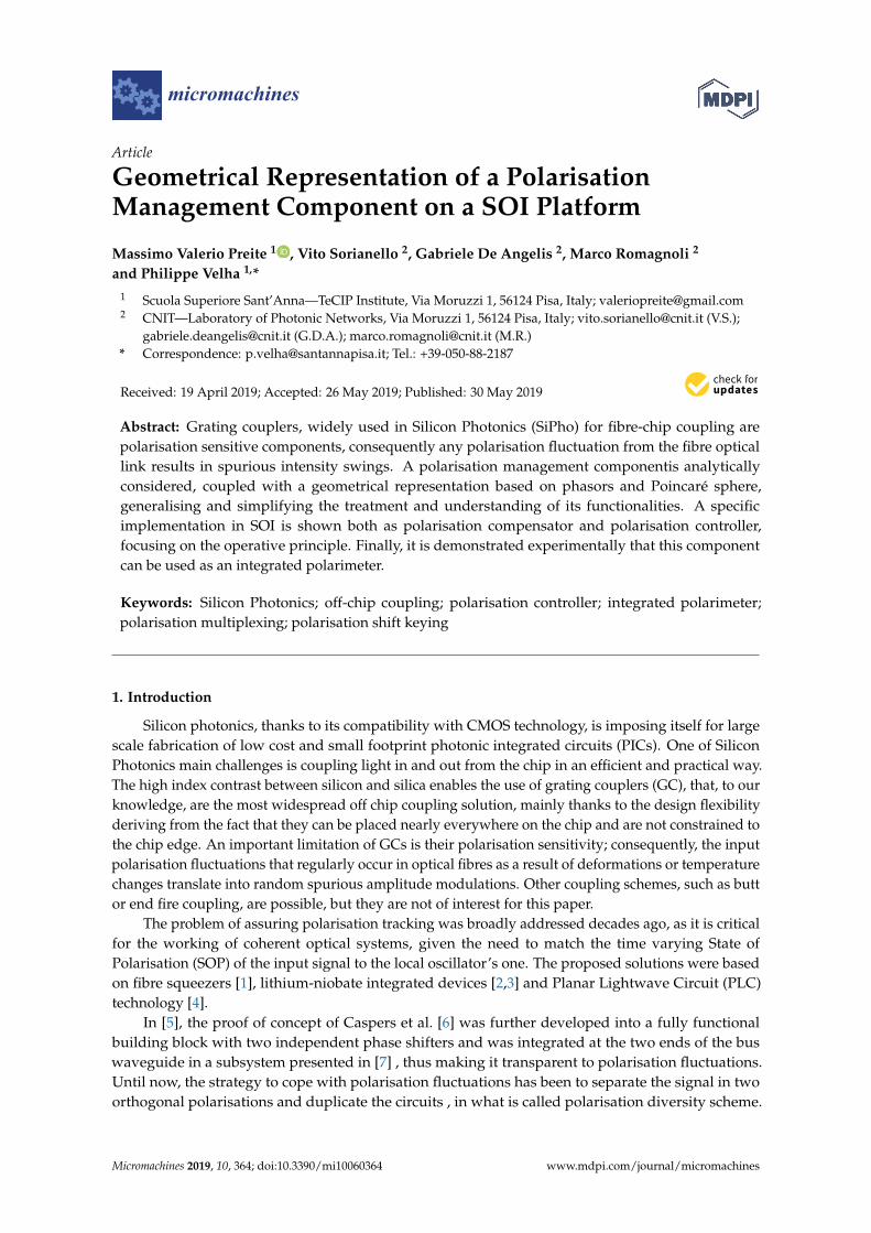


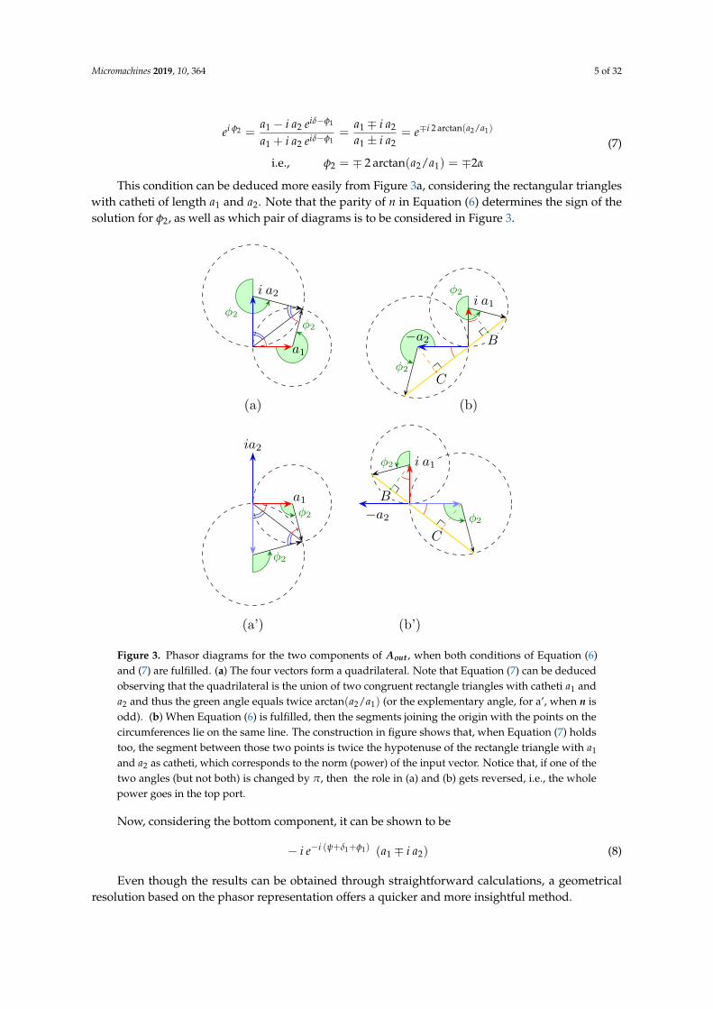


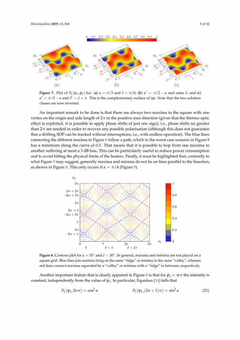


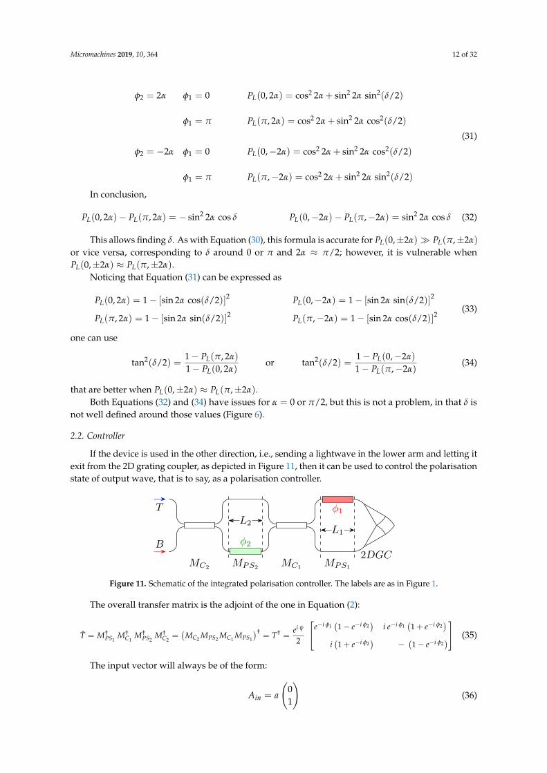


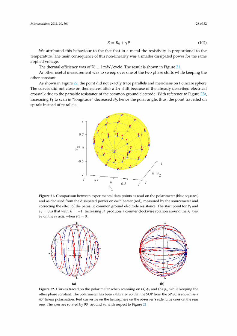


![[GAGIS]A Hierarchical Representation and Computation Scheme of Arbitrary-dimensional Geometrical Primitives Based on CGA](https://static.documents.pub/doc/80x56/58ae2b801a28ab557e8b4cb7/gagisa-hierarchical-representation-and-computation-scheme-of-arbitrary-dimensional.jpg)