GLAST LAT Project CAL Peer Design Review, Mar 17-18, 2003 P. Prat CNRS/IN2P3-LLR Ecole Polytechnique GLAST Large Area GLAST Large Area Telescope Telescope Calorimeter Subsystem Gamma-ray Large Gamma-ray Large Area Space Area Space Telescope Telescope 6.2 Thermal Design and Analysis Pierre Prat L.L.R. Ecole Polytechnique Calorimeter IN2P3 System Engineer [email protected]33–1–69–33–39–25
Transcript
GLAST LAT Project CAL Peer Design Review, Mar 17-18, 2003
P. Prat
CNRS/IN2P3-LLREcole Polytechnique
GLAST Large Area TelescopeGLAST Large Area TelescopeCalorimeter Subsystem
Gamma-ray Large Gamma-ray Large Area Space Area Space TelescopeTelescope
6.2 Thermal Design and Analysis
Pierre PratL.L.R. Ecole PolytechniqueCalorimeter IN2P3 System Engineer
GLAST LAT Project CAL Peer Design Review, Mar 17-18, 2003
P. Prat 6.2-2CNRS/IN2P3-LLR
Ecole Polytechnique
Thermal DesignThermal Design
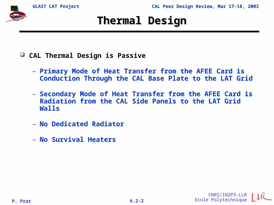
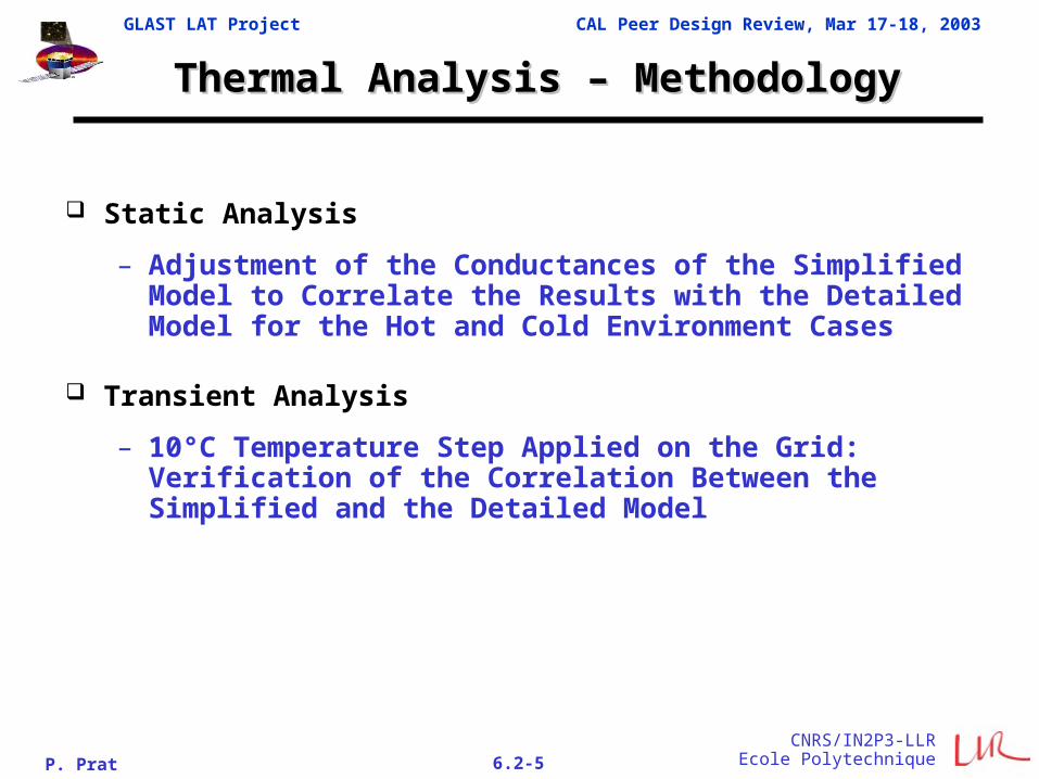
CAL Thermal Design is Passive
– Primary Mode of Heat Transfer from the AFEE Card is Conduction Through the CAL Base Plate to the LAT Grid
– Secondary Mode of Heat Transfer from the AFEE Card is Radiation from the CAL Side Panels to the LAT Grid Walls
– No Dedicated Radiator
– No Survival Heaters
GLAST LAT Project CAL Peer Design Review, Mar 17-18, 2003
P. Prat 6.2-3CNRS/IN2P3-LLR
Ecole Polytechnique
Thermal Design DriversThermal Design Drivers
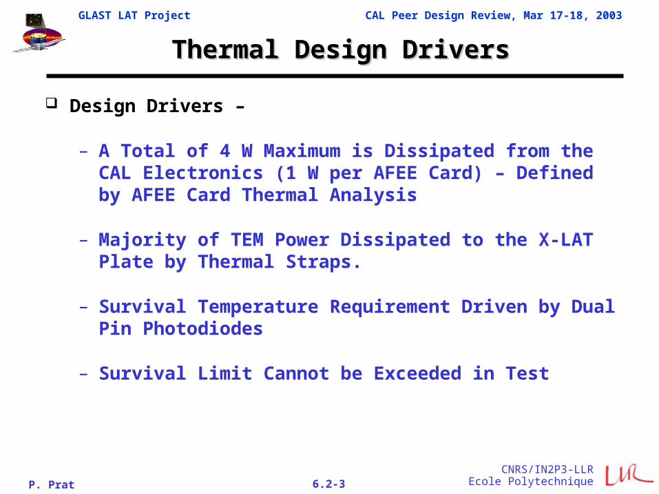
Design Drivers –
– A Total of 4 W Maximum is Dissipated from the CAL Electronics (1 W per AFEE Card) – Defined by AFEE Card Thermal Analysis
– Majority of TEM Power Dissipated to the X-LAT Plate by Thermal Straps.
– Survival Temperature Requirement Driven by Dual Pin Photodiodes
– Survival Limit Cannot be Exceeded in Test
GLAST LAT Project CAL Peer Design Review, Mar 17-18, 2003
P. Prat 6.2-4CNRS/IN2P3-LLR
Ecole Polytechnique
Thermal Analysis – TasksThermal Analysis – Tasks
Detailed Model of CAL Module
– Construction of the Detailed Model Reflecting Actual Design
– The Detailed Model Parameters Will Be Updated According to the Thermal Balance Test Measurements on the Engineering Module (In Particular, Contact Thermal Resistances Will Be Refined)
Detailed Model of AFEE Card – Presented in Section 7.0
Simplified Model of CAL Module
– Correlation of Results With Detailed Model
– Delivered to SLAC
GLAST LAT Project CAL Peer Design Review, Mar 17-18, 2003
GLAST LAT Project CAL Peer Design Review, Mar 17-18, 2003
P. Prat 6.2-9CNRS/IN2P3-LLR
Ecole Polytechnique
Thermal Model DescriptionThermal Model Description
– No Geometric Model
– Math Model (Not SINDA): Electrical Analogical Model Using the Orcad Pspice Simulation Software:
– Voltage (Volt) Temperature T (°C)– Current (Ampere) Power P (W)– Electrical Resistance (Ohm) Thermal Resistance (°C/W)– Electrical Capacitance (µF) Thermal Capacitance Cth (J/°C)– Time (µS) Time T (S)
– Simplified Thermal Model Simulation – Consists of 15 Nodes– Used for the Detailed LAT Thermal Model Simulation
– Detailed Thermal Model Simulation – Consists of 3150 Nodes– Objectives:
» Temperature Static Analysis in the Hot and Cold Cases» Temperature Transient Analysis: Determination of the Built-up Time
(CsI(Tl) Logs, Aluminum Plates, AFEE Boards)» Determine the Parameters Which Was Used for the Simplified
Thermal Model
GLAST LAT Project CAL Peer Design Review, Mar 17-18, 2003
P. Prat 6.2-10CNRS/IN2P3-LLR
Ecole Polytechnique
Simplified Thermal ModelSimplified Thermal Model
The Simplified Thermal Model Simulation Is Defined in the Document, LAT-TD-01163-03 (“CAL Simplified Simulation Thermal Model Definition”)
The CAL Consists of 15 Nodes As Follows:– 5 Nodes on the Aluminum Base-Plate– 1 Node on Each AFEE Board– 1 Node on Each Aluminum Side-Panel/Close-Out Plate Assembly
(Considered Each as a Single Plate)– 1 Node on the Center of the Composite Structure– 1 Node on the Top of the Composite Structure
Parameters:– Thermal Conductances Between Nodes (26)– Thermal Capacitances at Each Nodes (15)– Power Sources at Each AFEE Nodes (4)– Thermal Radiation Parameters (Surface , Emissivity) on Each
External Sides Nodes (6)
GLAST LAT Project CAL Peer Design Review, Mar 17-18, 2003
P. Prat 6.2-11CNRS/IN2P3-LLR
Ecole Polytechnique
Simplified Thermal ModelSimplified Thermal Model
N6 N4
N2
N3
N5 N1
N7
N8 N9 N11
N10
N12
N13
N15
X+
Y+
N14
GLAST LAT Project CAL Peer Design Review, Mar 17-18, 2003
P. Prat 6.2-12CNRS/IN2P3-LLR
Ecole Polytechnique
Detailed Thermal ModelDetailed Thermal Model
The Complete Simulation Thermal Model is Defined in the Document, GLAST-LLR-TN-054 (“Detailed Simulation Thermal Model Definition of a CAL Module”)
The CAL Model Consists of the Following Sub-Modules
– Base Plate: Modeled by a Plate of 5 X 5 Nodes
– 4 Close-Out Plates/Side Panels: Modeled as a Plate of 7 X 6 Nodes
– 4 AFEE Boards: Modeled as a Plate of 7 X 6 Nodes
– Top Frame: Modeled as a Frame of 16 Nodes
– Composite Structure With CDEs : Modeled by a Network of 2770 nodes
Radiative and Conductive Interfaces are Modeled with:
– LAT Grid (Radiative/Conductive)
– Tracker (Radiative)
– TEM (Radiative/Conductive)
GLAST LAT Project CAL Peer Design Review, Mar 17-18, 2003
P. Prat 6.2-13CNRS/IN2P3-LLR
Ecole Polytechnique
Detailed Thermal ModelDetailed Thermal Model
RL1-3
{Rlong}
RL1-1
{Rlong}
RL1-4
{Rlong}
RL1-2
{Rlong}
R2-3{Re}
R2-G{Rv }
R2-H
{Rh}
R2-D{Rv }
R3-H
{Rh}
R3-3{Re}
R3-G{Rv }
R3-B
{Rh}
R3-D{Rv }
R4-G{Rv }
R4-3{Re}
R4-D{Rv }
R4-B
{Rh}
R4-H
{Rh}
RL3-3
{Rlong}
RL3-1
{Rlong}
RL3-2
{Rlong}
RL4-3
{Rlong}
RL3-4
{Rlong}
R5-B
{Rh}
R5-H
{Rh}
R5-D{Rv }
R5-G{Rv }
R5-3{Re}
RL5-2
{Rlong}
RL5-1
{Rlong}
RL5-4
{Rlong}
RL5-3
{Rlong}
R2-2{Re}
C2{Cth}
C3{Cth}
R2-1{Re}
R3-2{Re}
C4{Cth}
R3-1{Re}
R4-2{Re}
R4-1{Re}
C5{Cth}
R5-1{Re}
R5-2{Re}
R6-G{Rv }
R6-B
{Rh}
R6-2{Re}
R6-H
{Rh}
C6{Cth}
R6-D{Rv } C7
{Cth}C8
{Cth}
RL6-1
{Rlong}
R7-1{Re}
R7-2{Re}
R6-1{Re}
R7-G
{Rv }
R6-3{Re}
R7-B
{Rh}
R7-D{Rv }
R7-H
{Rh}
RL7-1
{Rlong}
R7-3{Re}
RL7-3
{Rlong}
RL7-4
{Rlong}
RL7-2
{Rlong}
R8-D{Rv }
R8-G{Rv }
R8-H
{Rh}
R8-2{Re}
R8-1{Re}
R8-3{Re}
R9-1{Re}
R9-G{Rv }
R9-B
{Rh}
R9-2{Re}
C9{Cth}
R9-3{Re}
R9-H
{Rh}
R9-D{Rv }
RL9-4
{Rlong}
RL9-3
{Rlong}
R10-1{Re}
RL9-1
{Rlong}
R10-2{Re} R10-B
{Rh}
C10{Cth}
R10-D{Rv }
R10-H
{Rh}
R10-3{Re}
RL10-3
{Rlong}
R11-2{Re}
R11-1{Re}
R11-H
{Rh}
C11{Cth}
R11-B
{Rh}
RL11-1
{Rlong}
R11-D{Rv }
RL11-2
{Rlong}
RL11-3
{Rlong}
RL11-4
{Rlong}
R12-2{Re}
R12-1{Re}
C12{Cth}
R12-B
{Rh}
R12-H
{Rh}
R12-3{Re}
R12-D{Rv }
R12-4
{Re}
R10-4{Re} R11-4
{Re}R9-4
{Re}R7-4
{Re}
R8-4{Re}
R5-4{Re}
R6-4{Re}
R4-4{Re}
R2-4
{Re}
R3-4{Re}R2-B
{Rh}
RL2-1
{Rlong}
RL2-2
{Rlong}
RL2-4
{Rlong}
RL2-3
{Rlong}
RL4-1
{Rlong}
RL4-4
{Rlong}
RL4-2
{Rlong}
RL6-3
{Rlong}
RL6-4
{Rlong}
RL6-2
{Rlong}
RL8-2
{Rlong}
RL8-1
{Rlong}
RL10-1
{Rlong}
RL10-4
{Rlong}
RL10-2
{Rlong}
RL8-4
{Rlong}
RL9-2
{Rlong}
R8-B
{Rh}
R12-G{Rv }
R11-G{Rv }
R1-C
{Rcs i}
R2-C
{Rcs i}
R3-C
{Rcs i}
R4-C
{Rcs i}
R6-C
{Rcs i}
R5-C
{Rcs i}
R8-C
{Rcs i}
R7-C
{Rcs i}
R9-C
{Rcs i}
R11-C
{Rcs i}
R10-C
{Rcs i}
R10-G{Rv }
RL8-3
{Rlong}
R11-3{Re}
RL12-3
{Rlong}
RL12-1
{Rlong}
RL12-2
{Rlong}
R12-C
{Rcs i}
RL12-4
{Rlong}
C1{Cth/2}
R1-3{2*Re}
R1-1{2*Re}
R1-2{2*Re}
R1-4{2*Re}
R1-H
{2*Rh}
R1-D{2*Rv }
R1-B
{2*Rh}
R1-G
{2*Rv }
R13-3{2*Re}
R13-1{2*Re}
R13-4
{2*Re}R13-2{2*Re} R13-B
{2*Rh}
R13-D{2*Rv }
R13-H
{2*Rh}
R13-G{2*Rv } C13
{Cth/2}
00
N1-2
0
N2-3
N2-4N2-2
N2-1N1-3N1-1
N1-4
00000000 0
N4-2
N4-3N4-1
N3-4
N3-3
N3-2
N3-1
N6-4
N6-3N6-1N5-3
N5-4N5-2
N5-1
N4-4 N8-2
N8-3N8-1N7-3
N7-4N7-2
N7-1
N6-2
N10-3N10-1
N10-2
N9-1 N9-3
N9-4N9-2N8-4
N12-3
N12-2
N12-1
N11-4
N11-3
N11-2
N11-1
N10-4
0
N13-4
N13-3N13-1
N13-2N12-4 Composite CELL/CDE model diagram
R31{RLpcb1}
R30{RLpcb1}
R43{RLpcb1}
R32{RLpcb1}
R44{RLpcb1}
R54{RLpcb1}
R45{RLpcb1}
R55{RLpcb1}
R57{RLpcb1}
R56{RLpcb1}
R25
{RHpcb}
R58{RLpcb1}
R51
{RHpcb}
R21
{RHpcb}
R64
{RHpcb}
R47
{RHpcb}
R22
{RHpcb}
R60
{RHpcb}
R48
{RHpcb}
R35
{RHpcb}
R61
{RHpcb}
R36
{RHpcb}
R23
{RHpcb}0
R49
{RHpcb}
R24
{RHpcb}
R62
{RHpcb}
R50
{RHpcb}
R37
{RHpcb}
R63
{RHpcb}
R39
{RHpcb}
R26
{RHpcb}
R52
{RHpcb}
R67{RLpcb1}
R65
{RHpcb}
R69{RLpcb1}
R68{RLpcb1}
R70{RLpcb1}
R19{RLpcb2}
R71{RLpcb1}
R18{RLpcb2}
R17{RLpcb2}
R16{RLpcb2}
R42{RLpcb1}
R15{RLpcb2}
R29{RLpcb1}
R34
{RHpcb}
R28{RLpcb1}
R38
{RHpcb}
R14{RLpcb2*2}
R41{RLpcb1}
R20{RLpcb2*2}
R27{RLpcb1*2}
R40{RLpcb1*2}
R66{RLpcb1*2}
R53{RLpcb1*2}
R33{RLpcb1*2}
0
R59{RLpcb1*2}
R46{RLpcb1*2}
R77
{RHpcb*2}
R72{RLpcb1*2}
R73
{RHpcb*2}
R75
{RHpcb*2}
R74
{RHpcb*2}
R76
{RHpcb*2}
R1
{RHpcb*2}
R78
{RHpcb*2}
R3
{RHpcb*2}
R2
{RHpcb*2}
R4
{RHpcb*2}
R6
{RHpcb*2}
R5
{RHpcb*2}
I31+ -
I30+ -
I33+ -
I32+ -
I36+ -
I37+ -
I34+ -
I35+ -
I39+ -
I38+ -
I41+ -
I40+ -
I45+ -
I44+ -
I42+ -
I43+ -
I48+ -
I46+ -
I47+ -
I49+ -
PCB13
PCB12PCB8
PCB7PCB1
PCB28PCB27PCB26
PCB25PCB22
PCB21PCB17
PCB16
0
PCB5PCB4PCB3PCB2
PCB32PCB31PCB30PCB29
PCB19PCB18
PCB15PCB14
PCB11PCB10PCB9
PCB6
00
0
0
0
PCB24PCB23
PCB20
0
00
0
0
00
0
0
0
0
0
00
0
00
00000
00
C1
{Cpcb}
C2
{Cpcb}
C3
{Cpcb}
0
C4
{Cpcb}
C5
{Cpcb}
C6
{Cpcb}
C7
{Cpcb}
0
C8
{Cpcb}
C9
{Cpcb}
C10
{Cpcb}
0
C11
{Cpcb}
C12
{Cpcb}
C13
{Cpcb}
C14
{Cpcb}
0
C15
{Cpcb}
C16
{Cpcb}
C17
{Cpcb}
C18
{Cpcb}
0
C19
{Cpcb}
C20
{Cpcb}
0 0 0
R8
{Rbase}
R7
{Rbase}
R10
{Rbase}
R6
{Rbase}
R11
{Rbase}
R14
{Rbase}
R12
{Rbase}
R15
{Rbase}
R18
{Rbase}
R17
{Rbase}
R37
{Rbase}
R36
{Rbase}
R38
{Rbase}
R41
{Rbase}
R40
{Rbase}
R43
{Rbase}
TEM1
R45
{Rbase}
R44
{Rbase}
R47
{Rbase}
R46
{Rbase}
R48
{Rbase}
R50
{Rbase}
R53
{Rbase}
R51
{Rbase}
R65
{RinsB}
R60
{RinsB}
R75
{RinsB}
R70
{RinsB}
TEM2
R80
{RinsB}
R58
{RinsB}
R62
{RinsB}
R59
{RinsB}
R67
{RinsB}
R61
{RinsB}
R64
{RinsB}
R63
{RinsB}
R66
{RinsB}
R68
{RinsB}
R72
{RinsB}
R69
{RinsB}
TEM3
R71
{RinsB}
R73
{RinsB}
R76
{RinsB}
R77
{RinsB}
R74
{RinsB}
R82
{RinsB}
R78
{RinsB}
R81
{RinsB}
R88
{RintG}
R79
{RinsB}
R93
{RintG}
R94
{RintG}
R95
{RintG}
TEM4
R97
{RintG}
R96
{RintG}
R98
{RintG}
R100
{RintG}
R99
{RintG}
R89
{RintG}
R101
{RintG}
R90
{RintG}
R86
{RintG}
R91
{RintG}
R85
{RintG}
R1
{Rbase*2}
R84
{RintG}
R3
{Rbase*2}
R2
{Rbase*2}
R4
{Rbase*2}
R55
{Rbase*2}
R54
{Rbase*2}
R56
{Rbase*2}
R9
{Rbase*2}
R57
{Rbase*2}
R42
{Rbase*2}
R16
{Rbase*2}
R52
{Rbase*2}
R13
{Rbase*2}
R5
{Rbase*2}
R39
{Rbase*2}
R49
{Rbase*2}
C1{Cbase}
C11{Cbase}
C6{Cbase}
C16{Cbase}
C2{Cbase}
C21{Cbase}
C3{Cbase}
C5{Cbase}C4{Cbase}
C7{Cbase} C8{Cbase}C9
{Cbase}
C12{Cbase}
C10{Cbase}
C13{Cbase}
C15{Cbase}
C14{Cbase}
C18{Cbase}
C17{Cbase}
C19{Cbase}
C22{Cbase}
C20{Cbase}
C23{Cbase}
C25{Cbase}
C24{Cbase}
P9
P10
P17
P18
P19
P20
Q18
Q13
Q8
Q3
P16
P6
P7
P8
Q9Q10 Q6
Q2Q4Q5 Q1
Q23
Q17 Q16Q20
Q12Q14Q15 Q11
Q7
P3P2P1
Q24 Q22 Q21Q25
Q19
G1
P15 P14 P13 P12 P11
P5P4
G9
G8
G7
G6
G5G4G3G2
0
G16
G15
G14
G13 G12 G11 G10
0000
0000
00
00000
0
00000
000
AFEE board model diagram Base-plate model diagram
GLAST LAT Project CAL Peer Design Review, Mar 17-18, 2003
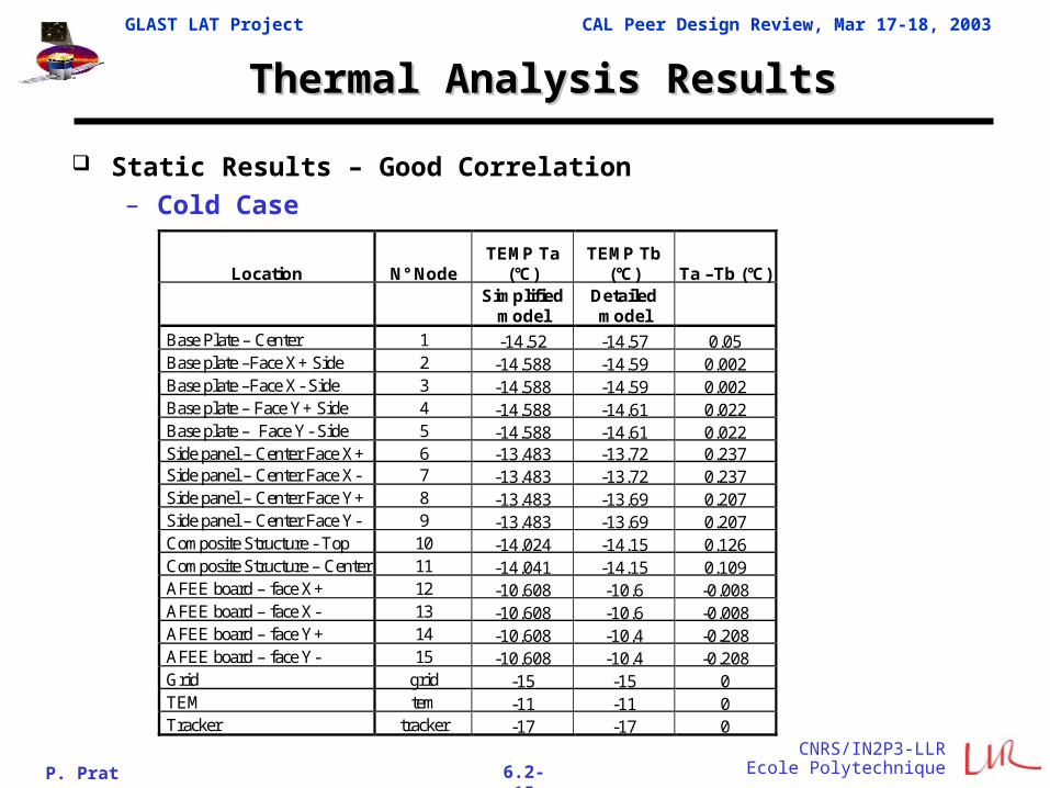
P. Prat 6.2-14CNRS/IN2P3-LLR
Ecole Polytechnique
Thermal Analysis ResultsThermal Analysis Results
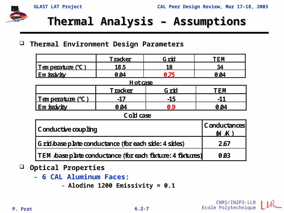
Static Results – Good Correlation– Hot Case
Location N° Node TEMP Ta
(°C) TEMP Tb
(°C) Ta –Tb (°C)
Simplified model
Detailed model
Base Plate – Center 1 18.74 18.64 0.1 Base plate –Face X+ Side 2 18.542 18.55 -0.008 Base plate –Face X- Side 3 18.542 18.55 -0.008 Base plate – Face Y+ Side 4 18.542 18.53 0.012 Base plate – Face Y- Side 5 18.542 18.53 0.012 Side panel – Center Face X+ 6 19.64 19.4 0.24 Side panel – Center Face X- 7 19.64 19.4 0.24 Side panel – Center Face Y+ 8 19.64 19.43 0.21 Side panel – Center Face Y- 9 19.64 19.43 0.21 Composite Structure - Top 10 19.188 19.02 0.168 Composite Structure – Center 11 19.171 19.01 0.161 AFEE board – face X+ 12 22.515 22.52 -0.005 AFEE board – face X- 13 22.515 22.52 -0.005 AFEE board – face Y+ 14 22.515 22.51 0.005 AFEE board – face Y- 15 22.515 22.51 0.005 Grid grid 18 18 0 TEM tem 34 34 0 Tracker tracker 18.5 18.5 0
GLAST LAT Project CAL Peer Design Review, Mar 17-18, 2003
P. Prat 6.2-15CNRS/IN2P3-LLR
Ecole Polytechnique
Thermal Analysis ResultsThermal Analysis Results
Static Results – Good Correlation
– Cold Case
Location N° Node TEMP Ta
(°C) TEMP Tb
(°C) Ta –Tb (°C)
Simplified
model Detailed model
Base Plate – Center 1 -14.52 -14.57 0.05 Base plate –Face X+ Side 2 -14.588 -14.59 0.002 Base plate –Face X- Side 3 -14.588 -14.59 0.002 Base plate – Face Y+ Side 4 -14.588 -14.61 0.022 Base plate – Face Y- Side 5 -14.588 -14.61 0.022 Side panel – Center Face X+ 6 -13.483 -13.72 0.237 Side panel – Center Face X- 7 -13.483 -13.72 0.237 Side panel – Center Face Y+ 8 -13.483 -13.69 0.207 Side panel – Center Face Y- 9 -13.483 -13.69 0.207 Composite Structure - Top 10 -14.024 -14.15 0.126 Composite Structure – Center 11 -14.041 -14.15 0.109 AFEE board – face X+ 12 -10.608 -10.6 -0.008 AFEE board – face X- 13 -10.608 -10.6 -0.008 AFEE board – face Y+ 14 -10.608 -10.4 -0.208 AFEE board – face Y- 15 -10.608 -10.4 -0.208 Grid grid -15 -15 0 TEM tem -11 -11 0 Tracker tracker -17 -17 0
GLAST LAT Project CAL Peer Design Review, Mar 17-18, 2003
P. Prat 6.2-16CNRS/IN2P3-LLR
Ecole Polytechnique
Thermal Analysis ResultsThermal Analysis Results Transient Results – Good Correlation
– A 10°C Temperature Step was Applied on the Grid in Order to Verify the Correlation Between the Simplified and Detailed Models
Transient Response - Complex Model
0
2
4
6
8
10
12
14
16
0 20000 40000 60000 80000 100000
Time (s)
Te
mp
era
ture
(°C
) AFEE Y - Center
Side-panel Y - Center
Comp. Structure - Top
Comp. Structure - Center
Base-plate - Center
Transient Response - Simplified Model
0
2
4
6
8
10
12
14
16
0 20000 40000 60000 80000 100000
Time (s)
Te
mp
era
ture
(°C
) AFEE Y - Center (D14)
Side-panel Y - Center (D8)
Comp. Structure - Top (D10)
Comp. Structure - Center (D11)
Base-plate - Center (D1)
GLAST LAT Project CAL Peer Design Review, Mar 17-18, 2003
P. Prat 6.2-17CNRS/IN2P3-LLR
Ecole Polytechnique
Thermal Design StatusThermal Design Status
Detailed and Simplified Thermal Models Have Been Developed with Material and Thermal Contact Assumptions
The Temperature Build-Up Time of the CDEs is Very Dependent on the Contact Resistances Between Parts (Aluminum-Composite, Titanium-Aluminum, CDE-Composite):
– 24:30 hr – 32:00 hr for the Qualification Thermal Cycle
• A Step of Temperature Applied on the Grid: –30°C to +50°C With a Temperature Slope of 10°C / Hour
• Time Determined at +49°C
• Min and Max Contact Thermal Resistances are in a Ratio 1:12
GLAST LAT Project CAL Peer Design Review, Mar 17-18, 2003
P. Prat 6.2-18CNRS/IN2P3-LLR
Ecole Polytechnique
Thermal Design Status - ContinuedThermal Design Status - Continued
The Detailed and Simplified Models Will Be Updated According to the Thermal Balance Test Results Achieved on the EM
– Model Update Will Only Affect the Parameter Values
– The Model of the Structure Will Not Change
The Current Thermal Simulations Show That the Thermal Design Is Sound:
– The Max Difference of Temperature Between CDEs is 0.7°C, Accounting for Max Values of Contact Thermal Resistances