Halogen and Antimony Free. “Green” Device (Note 3)
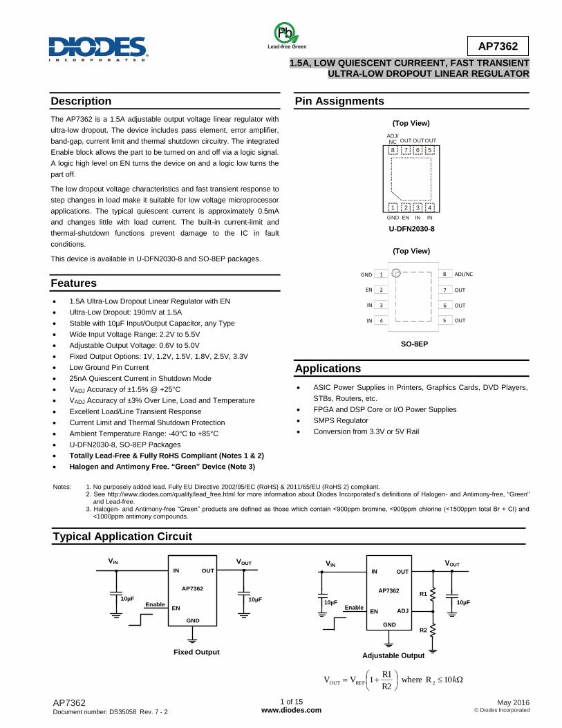
Pin Assignments
(Top View)
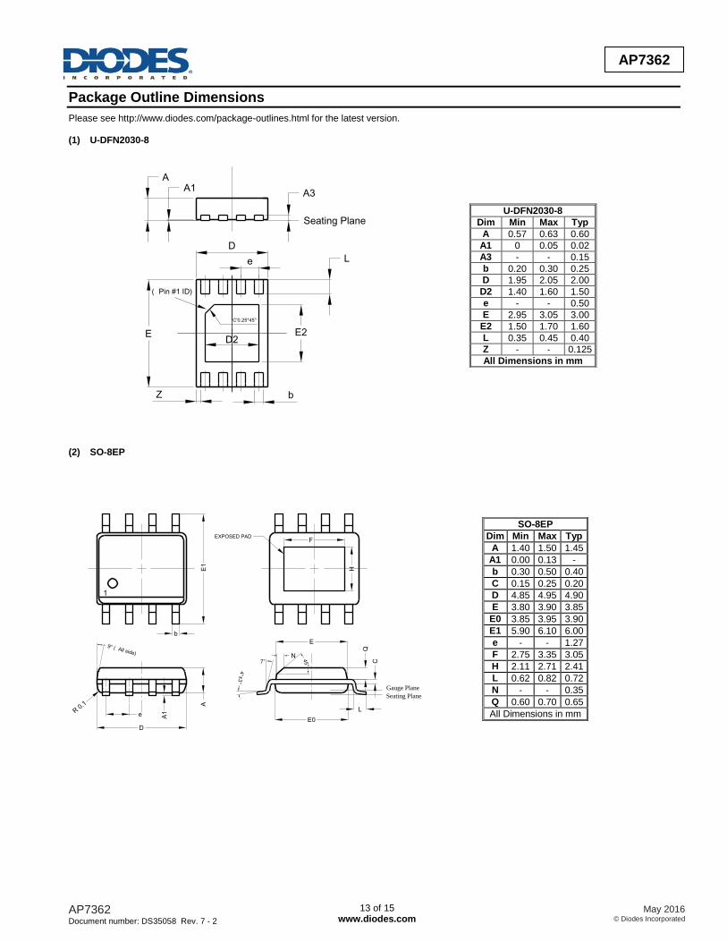
SO-8EP
Applications
ASIC Power Supplies in Printers, Graphics Cards, DVD Players,
STBs, Routers, etc.
FPGA and DSP Core or I/O Power Supplies
SMPS Regulator
Conversion from 3.3V or 5V Rail
Notes: 1. No purposely added lead. Fully EU Directive 2002/95/EC (RoHS) & 2011/65/EU (RoHS 2) compliant. 2. See http://www.diodes.com/quality/lead_free.html for more information about Diodes Incorporated’s definitions of Halogen- and Antimony-free, "Green" and Lead-free. 3. Halogen- and Antimony-free "Green” products are defined as those which contain <900ppm bromine, <900ppm chlorine (<1500ppm total Br + Cl) and <1000ppm antimony compounds.
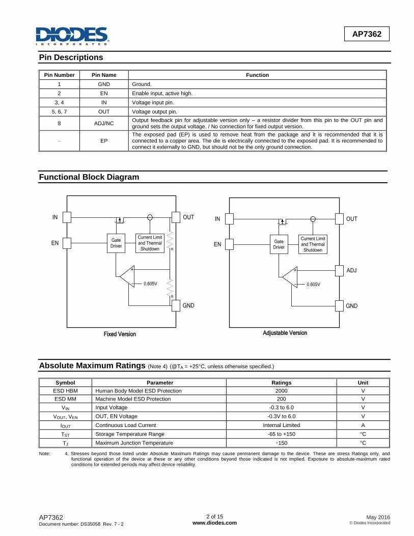
8 ADJ/NC Output feedback pin for adjustable version only – a resistor divider from this pin to the OUT pin and ground sets the output voltage. / No connection for fixed output version.
– EP The exposed pad (EP) is used to remove heat from the package and it is recommended that it is connected to a copper area. The die is electrically connected to the exposed pad. It is recommended to connect it externally to GND, but should not be the only ground connection.
Note: 4. Stresses beyond those listed under Absolute Maximum Ratings may cause permanent damage to the device. These are stress Ratings only, and functional operation of the device at these or any other conditions beyond those indicated is not implied. Exposure to absolute-maximum rated conditions for extended periods may affect device reliability.
TJ Operating Junction Temperature (Note 5) -40 +125 C
Note: 5. Operating junction temperature must be evaluated and derated as needed, based on ambient temperature (TA), power dissipation (PD), maximum
allowable operating junction temperature (TJ-MAX), and package thermal resistance (θJA).
Electrical Characteristics (@TA = +25°C, VIN
= 3.3V, VOUT =1.8V, IOUT = 10mA, VEN = VIN, CIN
= 10μF, COUT
= 10μF, VEN
= 2V, unless otherwise stated.)
Minimum and maximum limits are guaranteed through test, design, or statistical correlation. Typical values represent the most likely parametric
norm at TA = +25°C, and are provided for reference purposes only.
Symbol Parameter Test Conditions Min Typ Max Unit
VADJ
ADJ Pin Voltage VIN = VIN-MIN to VIN-MAX,
IOUT = 10mA to 1.5A
TA = +25°C 0.584 0.605 0.626 V
Over temp 0.575 – 0.635
ADJ Pin Voltage (A Grade) VIN = VIN-MIN to VIN-MAX,
IOUT = 10mA to 1.5A
TA = +25°C 0.596 0.605 0.614 V
Over temp 0.587 – 0.623
IADJ ADJ Pin Bias Current VIN = VIN-MIN to VIN-MAX TA = +25°C – 50 –
nA Over temp – – 750
VDROPOUT Dropout Voltage (Note 6) IOUT = 1.5A, VOUT = 2.5V TA = +25°C – 190 240
mV Over temp – – 280
VOUT/VIN Line Regulation (Note 7) VIN = VIN-MIN to VIN-MAX TA = +25°C – 0.04 –
%/V Over temp – 0.05 –
VOUT/IOUT Load Regulation (Note 7) IOUT = 10mA to 1.5A TA = +25°C – 0.18 –
%/A Over temp – 0.33 –
IGND Ground Pin Current in Normal Operation Mode
IOUT = 10mA to 1.5A TA = +25°C – 1 1.2
mA Over temp – – 1.3
ISHDN Ground Pin Current VEN < VIL TA = +25°C – 0.025 0.125
μA Over temp – – 15
IOUT-PK Peak Output Current VOUT VOUT-NOM -5% – 3.6 – A
ISC Short Circuit Current OUT Grounded TA = +25°C – 3.7 –
A Over temp 2 – –
VIH Enable Logic High VIN = VIN-MIN to VIN-MAX Over temp 1.4 – – V
VIL Enable Logic Low VIN = VIN-MIN to VIN-MAX Over temp – – 0.65
IIH Enable Pin High Current VEN = VIN – 1 – nA
IIL Enable Pin Low Current VEN = 0V – 0.1 –
tD(OFF) Turn-Off Delay From VEN < VIL to VOUT = OFF, IOUT = 1.5A – 25 – μs
tD(ON) Turn-On Delay From VEN > VIH to VOUT = ON, IOUT = 1.5A – 25 – μs
Notes: 6. Dropout voltage is the minimum voltage difference between the input and the output at which the output voltage drops 2% below its nominal value. For any output voltage less than 2.5V, the minimum VIN operating voltage is the limiting factor. 7. The line and load regulation specification contains only the typical number. However, the limits for line and load regulation are included in the adjust voltage tolerance specification.
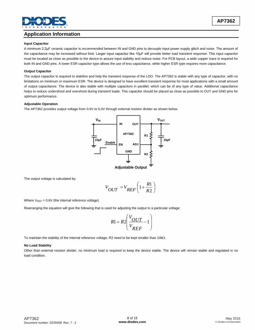
A minimum 2.2μF ceramic capacitor is recommended between IN and GND pins to decouple input power supply glitch and noise. The amount of
the capacitance may be increased without limit. Larger input capacitor like 10μF will provide better load transient response. This input capacitor
must be located as close as possible to the device to assure input stability and reduce noise. For PCB layout, a wide copper trace is required for
both IN and GND pins. A lower ESR capacitor type allows the use of less capacitance, while higher ESR type requires more capacitance. Output Capacitor
The output capacitor is required to stabilize and help the transient response of the LDO. The AP7362 is stable with any type of capacitor, with no
limitations on minimum or maximum ESR. The device is designed to have excellent transient response for most applications with a small amount
of output capacitance. The device is also stable with multiple capacitors in parallel, which can be of any type of value. Additional capacitance
helps to reduce undershoot and overshoot during transient loads. This capacitor should be placed as close as possible to OUT and GND pins for
optimum performance. Adjustable Operation
The AP7362 provides output voltage from 0.6V to 5.0V through external resistor divider as shown below.
The output voltage is calculated by:
2
11
R
R
REFV
OUTV
Where VREF = 0.6V (the internal reference voltage) Rearranging the equation will give the following that is used for adjusting the output to a particular voltage:
121
REFV
OUTV
RR
To maintain the stability of the internal reference voltage, R2 need to be kept smaller than 10k. No Load Stability
Other than external resistor divider, no minimum load is required to keep the device stable. The device will remain stable and regulated in no
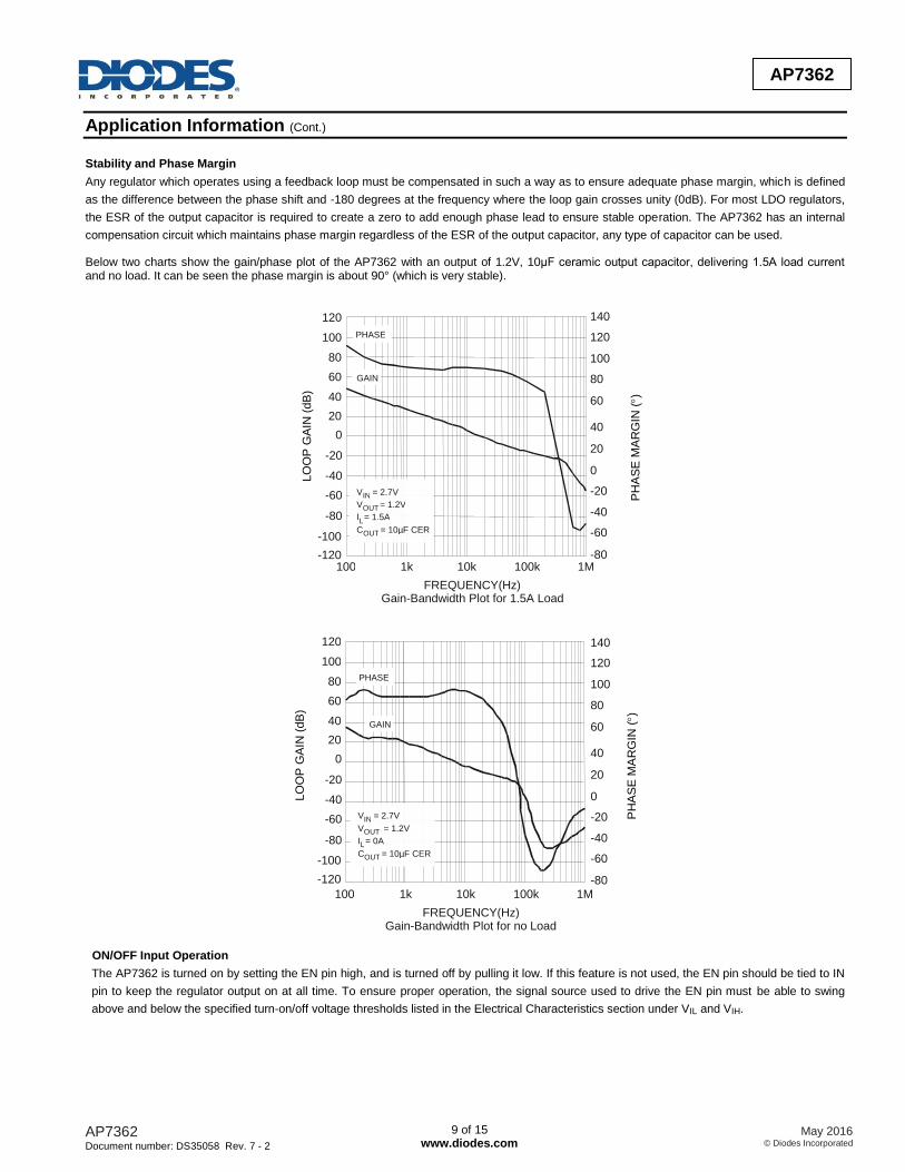
Any regulator which operates using a feedback loop must be compensated in such a way as to ensure adequate phase margin, which is defined
as the difference between the phase shift and -180 degrees at the frequency where the loop gain crosses unity (0dB). For most LDO regulators,
the ESR of the output capacitor is required to create a zero to add enough phase lead to ensure stable operation. The AP7362 has an internal
compensation circuit which maintains phase margin regardless of the ESR of the output capacitor, any type of capacitor can be used. Below two charts show the gain/phase plot of the AP7362 with an output of 1.2V, 10μF ceramic output capacitor, delivering 1.5A load current and no load. It can be seen the phase margin is about 90° (which is very stable).
ON/OFF Input Operation
The AP7362 is turned on by setting the EN pin high, and is turned off by pulling it low. If this feature is not used, the EN pin should be tied to IN
pin to keep the regulator output on at all time. To ensure proper operation, the signal source used to drive the EN pin must be able to swing
above and below the specified turn-on/off voltage thresholds listed in the Electrical Characteristics section under VIL and VIH.
IMPORTANT NOTICE DIODES INCORPORATED MAKES NO WARRANTY OF ANY KIND, EXPRESS OR IMPLIED, WITH REGARDS TO THIS DOCUMENT, INCLUDING, BUT NOT LIMITED TO, THE IMPLIED WARRANTIES OF MERCHANTABILITY AND FITNESS FOR A PARTICULAR PURPOSE (AND THEIR EQUIVALENTS UNDER THE LAWS OF ANY JURISDICTION). Diodes Incorporated and its subsidiaries reserve the right to make modifications, enhancements, improvements, corrections or other changes without further notice to this document and any product described herein. Diodes Incorporated does not assume any liability arising out of the application or use of this document or any product described herein; neither does Diodes Incorporated convey any license under its patent or trademark rights, nor the rights of others. Any Customer or user of this document or products described herein in such applications shall assume all risks of such use and will agree to hold Diodes Incorporated and all the companies whose products are represented on Diodes Incorporated website, harmless against all damages. Diodes Incorporated does not warrant or accept any liability whatsoever in respect of any products purchased through unauthorized sales channel. Should Customers purchase or use Diodes Incorporated products for any unintended or unauthorized application, Customers shall indemnify and hold Diodes Incorporated and its representatives harmless against all claims, damages, expenses, and attorney fees arising out of, directly or indirectly, any claim of personal injury or death associated with such unintended or unauthorized application. Products described herein may be covered by one or more United States, international or foreign patents pending. Product names and markings noted herein may also be covered by one or more United States, international or foreign trademarks. This document is written in English but may be translated into multiple languages for reference. Only the English version of this document is the final and determinative format released by Diodes Incorporated.
LIFE SUPPORT Diodes Incorporated products are specifically not authorized for use as critical components in life support devices or systems without the express written approval of the Chief Executive Officer of Diodes Incorporated. As used herein: A. Life support devices or systems are devices or systems which: 1. are intended to implant into the body, or
2. support or sustain life and whose failure to perform when properly used in accordance with instructions for use provided in the labeling can be reasonably expected to result in significant injury to the user.