13
GolclStar MONOCHROME MONITOR SERVICE MANUAL WTION BEFORE SERVICING THE CHASSIS, READ THE “SAFETY PREtXJTK)NS”, IN THIS MANUAL MODEL: MBM-2105GIA (MC-3 CHA=W B GoldStar
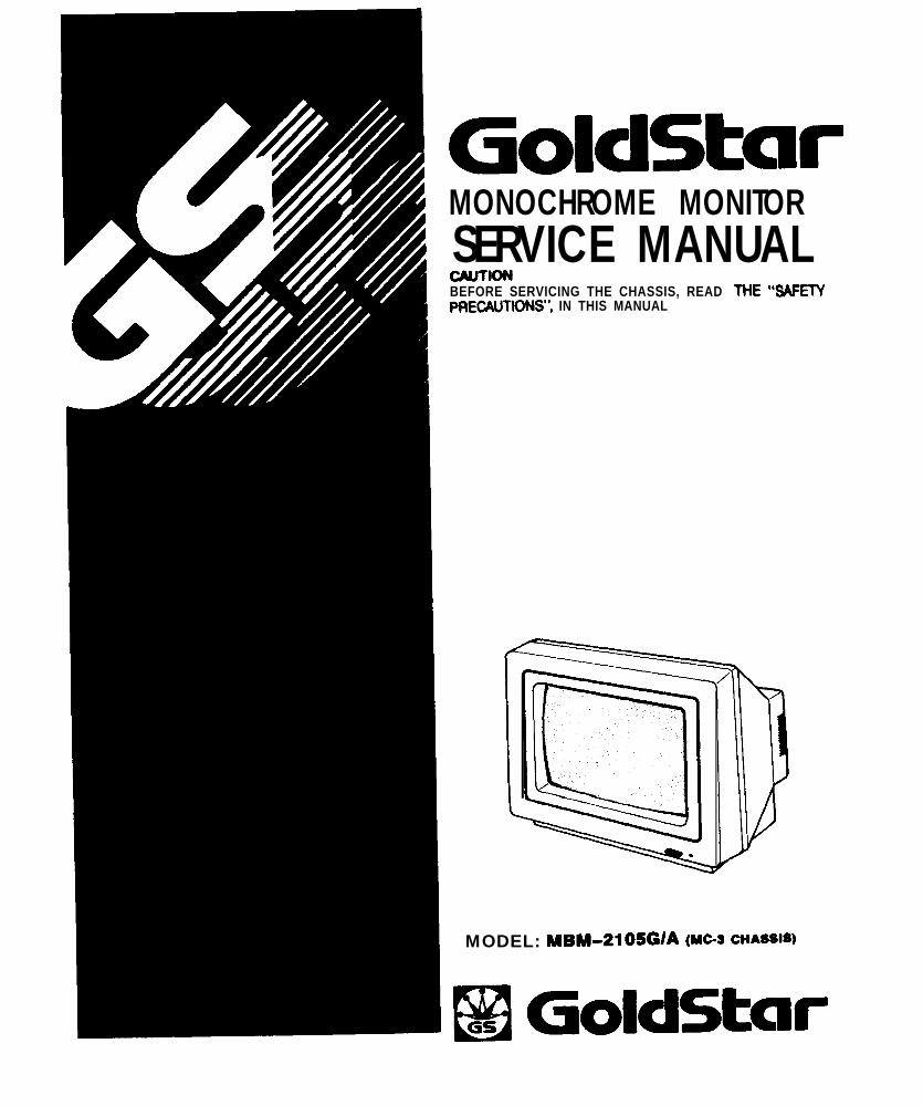
GolclStarMONOCHROME MONITORSERVICE MANUALWTIONBEFORE SERVICING THE CHASSIS, READ THE “SAFETYPREtXJTK)NS”, IN THIS MANUAL
MODEL: MBM-2105GIA (MC-3 CHA=W
B GoldStar
FEATURES
l 2000 display characters in a 8 x 8 dot format.l 18 MHz bandwidth, medium class, composite signal input.l This monitor is compatible with a variety of home and personal computers
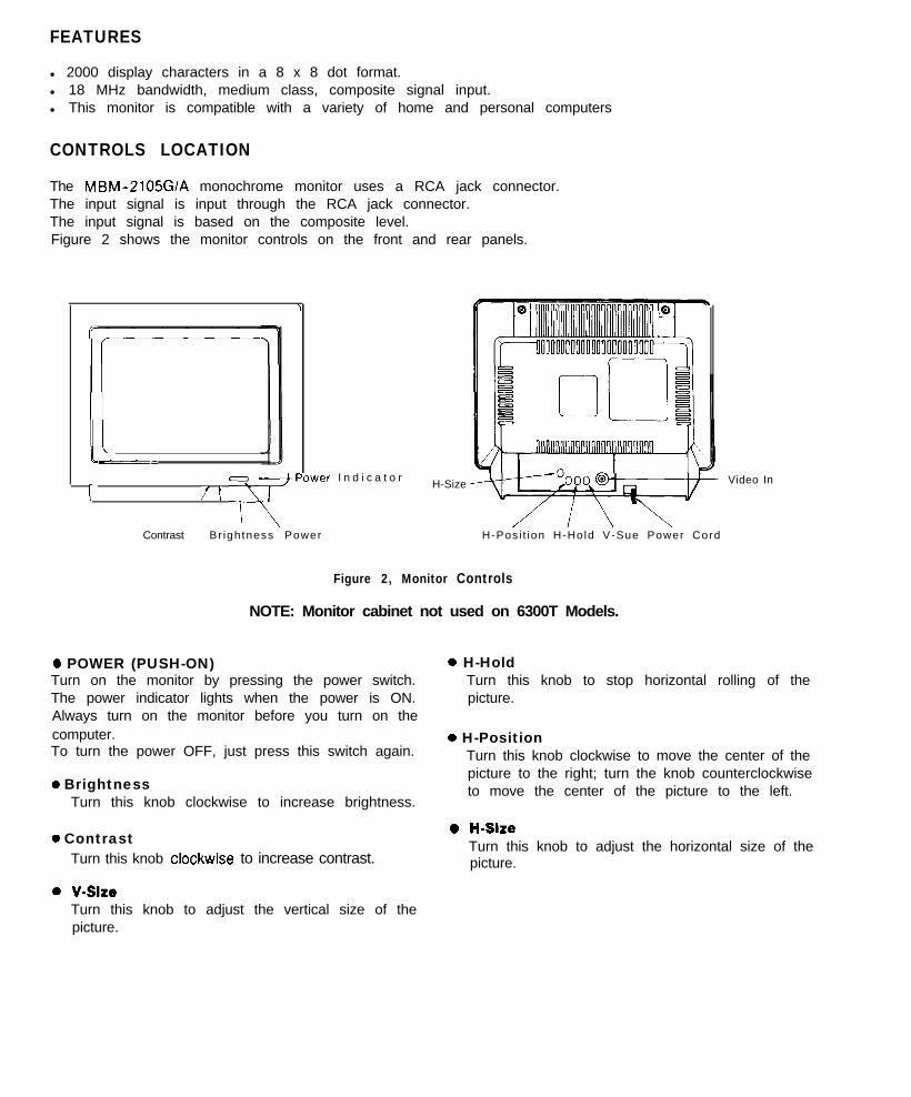
CONTROLS LOCATION
The MBM-2105GIA monochrome monitor uses a RCA jack connector.The input signal is input through the RCA jack connector.The input signal is based on the composite level.Figure 2 shows the monitor controls on the front and rear panels.
\
[
r-----
/ t yLcPower I n d i c a t o r H-Size Video In
IContrast Br ightness Power H-Pos i t ion H-Hold V-Sue Power Cord
Figure 2, Monitor Controls
NOTE: Monitor cabinet not used on 6300T Models.
0 POWER (PUSH-ON)Turn on the monitor by pressing the power switch.The power indicator lights when the power is ON.Always turn on the monitor before you turn on thecomputer.To turn the power OFF, just press this switch again.
0 BrightnessTurn this knob clockwise to increase brightness.
0 ContrastTurn this knob clockvvise to increase contrast.
0 V-SizeTurn this knob to adjust the vertical size of thepicture.
0 H-HoldTurn this knob to stop horizontal rolling of thepicture.
0 H-PositionTurn this knob clockwise to move the center of thepicture to the right; turn the knob counterclockwiseto move the center of the picture to the left.
0 H-SizeTurn this knob to adjust the horizontal size of thepicture.
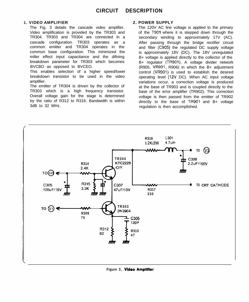
CIRCUIT DESCRIPTION
1. VIDEO AMPLIFIER 2. POWER SUPPLYThe Fig. 3 details the cascade video amplifier.Video amplification is provided by the TR303 andTR304. TR303 and TR304 are connected in acascade configuration. TR303 operates as acommon emitter and TR304 operates in thecommon base configuration. This minimized themiller effect input capacitance and the difiningbreakdown parameter for TR303 which becomesBVCBO as opposed to BVCEO.This enables selection of a higher speed/lowerbreakdown transistor to be used in the videoamplifier.The emitter of TR304 is driven by the collector ofTR303 which is a high frequency transistor.Overall voltage gain for the stage is determinedby the ratio of R312 to R316. Bandwidth is within
The 120V AC line voltage is applied to the primaryof the T901 where it is stepped down through thesecondary winding to approximately 17V (AC).After passing through the bridge rectifier circuitand filter (C905) the regulated DC supply voltageis approximately 18V (DC). The 18V unregulatedB+ voltage is applied directly to the collector of theB+ regulator (TR901). A voltage divider network(R905, VR901, R906) in which the B+ adjustmentcontrol (VR901) is used to establish the desiredoperating level (12V DC). When AC input voltagevariations occur, a correction voltage is producedat the base of TR903 and is coupled directly to thebase of the error amplifier (TR902). This correctionvoltage is then passed from the emitter of TR902directly to the base of TR901 and B+ voltageregulation is then accomplished.3dB to 32 MHz.
TO@
c305lOOuF/
TO @
R316 L3011 .ZK/ZW 4.7uH
7 l TO+
T R 3 0 4 2~ C308R314 KTC2229 2.2uFll
< ;
+l TO
‘16V R3173 3 0
3 T R 3 0 32N3904
C30612OP
R3097 5
R3134 7
0v
oov
CRT CA.THODE
Figure 3, Video Ampllfler

VerticalOscillator
F,B)vcc 2
Vetical FrameVcc 2 Generator
1 Oscillator 1
Frame-Synchro
Generator
Line Fly Back PhaseInput Detector
HorizontalOscillator
Verticalo u t p u t
P o w e rAmplifierInput
Horizontaloutput
Figure 4, BLOCK DIAGRAM OF THE TEA 2037A
3. COMPOSITE VIDEO INPUT AND HORIZONTAL/VERTICAL DEFLECTION
3-l VIDEO INPUT (PIN 15) 3-3The detection level for negative sync pulse at thesync separation input (pin 15) is set at 1.6V. Whenthe voltage at emitter of the Transistor (pin 15) isabove 1.6V, the transistor is cut off. Voltagelower than 1.6V enables the transistor to conducta n d t h e internal circuitry i s enabled forsynchronization function.
3-4
LINE (H) OSCILLATOR (PIN 9)The line oscillator is of the type which charges anddischarges a capacitor, since a perfectly linearsawtooth wave form is not required.The free running frequency is dependent on C705,R705 and VR702 and is governed by this expres-sion To = 085 x C705 x R705 where To is the lineoscillator free running frequency.
FRAME(V) OSCILLATOR (PIN 9)Oscillator thresholds are internally fixed byresistor C601, R603 are used to determine thefree-running frequency, the oscillatorfree-running frequency is given by To = 0.15 xC601 x R603.
3-2 COMPOSITE VIDEO INPUT (PIN 15)
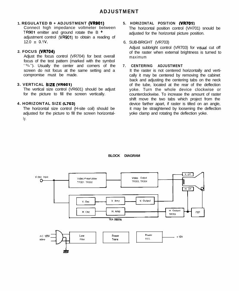
ADJUSTMENT
1. REGULATED B + ADJUSTMENT (VRSOl)Connect high impedance voltmeter betweenTR901 emitter and ground rotate the B +adjustment control (VR901) to obtain a reading of12.0 2 O.lV.
2. FOCUS (VR704)Adjust the focus control (VR704) for best overallfocus of the test pattern (marked with the symbol“%“). Usually the center and corners of thescreen do not focus at the same setting and acompromise must be made.
3. VERTICAL SIZE (VR601)The vertical size control (VR601) should be adjustfor the picture to fill the screen vertically.
4. HORIZONTAL SIZE (L703)The horizontal size control (H-site coil) should beadjusted for the picture to fill the screen horizontal-ly.
5. HORIZONTAL POSITION NR701)The horizontal position control (VH701) snould beadjusted for the horizontal picture position.
6. SUB-BRIGHT (VR703)Adjust subbright control (VR703) for visual cut offof the raster when external brightness is turned tomaximum
7. CENTERING ADJUSTMENTIt the raster is not centered horizontally and verti-cally it may be centered by removing the cabinetback and adjusting the centering tabs on the neckof the tube, located at the rear of the deflectionyoke. Turn the whole device clockwise orcounterclockwise. To increase the amount of rastershift move the two tabs which project from thedevice farther apart, if raster is tilted on an angle,it may be straightened by loosening the deflectionyoke clamp and rotating the deflection yoke.
BLOCK DIAGRAM
V,deo Input
0Video Preamphf~er
TR301. TR302
Video OutputTR303, TR304
TEA 2037A
AC 12OV LllW POW&Y PW+.?rR E G .
, +12v60Hz Filter TMlS
-
I
-
!
-
4
-
3
-
2
-
1
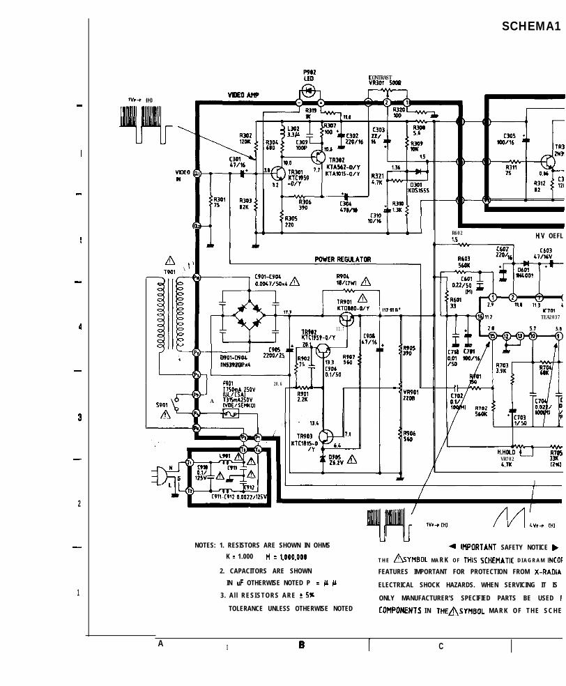
SCHEMA1
CONTRASTVR301 5008
t-
c9050901-0904 2200/2!
lN5392GP.4
1 F901 20.6T750mA 25OV
AIUL/CSAI1315mA25OVNDE/SEtlKOI
TR902 1 2 . 7
Kltl959-O/Y C908
R60215 H.V OEFL..-
+y-+$ll.2 TEA2037
MnJ%- 4thH.HOLD u R705VR702 33Kb.lK 12Ul
I
NOTES: 1. RESISTORS ARE SHOWN IN OHMS
K = 1.000 M = 1.000.000
2. CAPACITORS ARE SHOWN
IN UF OTHERWISE NOTED P : cc Ir
3. All RESISTORS ARE f 5%
TOLERANCE UNLESS OTHERWISE NOTED
u u4 ItlPORTANT SAFETY NOTICE b
T H E SYMBOL MA RK O F THIS SCHEHATIC D I A G R A M INCOI
FEATURES IMPORTANT FOR PROTECTION FROM X-RADIA
ELECTRICAL SHOCK HAZARDS. WHEN SERVICING IT IS
ONLY MANUFACTURER’S SPECIFIED PARTS BE USED F
COl’lPONENTS IN THE&YUBOL MARK OF THE SCHE
A I B I C
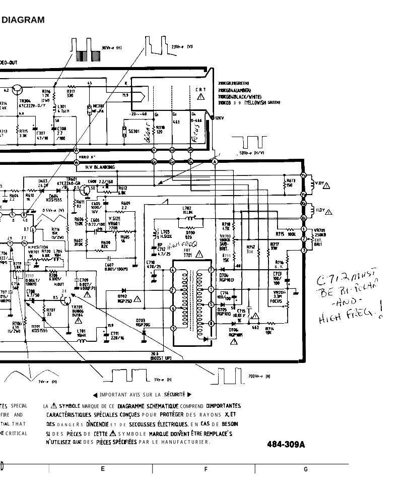
DIAGRAM
3OvI+ IHI
/
N-i
23VI-r IV1
9lOKGB3UGREENl
mKGB4*wmENl
9lDKMUBLACK/WHTE)
9lDKGB 3 9 IYELLOWISH GREEN1
/ - 5OVP-P M/VI
-H.LW. 0 ;
RltOb7K
VR703 R7K 1ooK
BRJT. R7u3 3 K
R 7 1 1l5K
R7Y6 . Y
070) cm
RGPlOD lw/100 ‘?
01G.h R719 : vR7052sOKnEXT.BRIT
f
;;,2 ,/,6ti cn@FBT
&l/l5 7701 A
, *I 1
c 7 1 7 R7OI 1 1OwLI/ L.wvloowl tl.OUl
c70832 0
L.7/50 _.c7l4
o%ll l!!z’
FOilIS
1’05 5 c7l5!rl!JEu3wl 0 . 0 1 / AlK
Lltw 6‘3 &lbRIM‘711
\ \ (BOOST UP1 \
& \I-Ln 3Vr-r IHI ‘-- 2oovp+ IH’
4 IMPORTANT AVIS SUR LA SkURlTi. b
TES SPECIAL
FIRE AND
IllAL T H A T
iE CRITICAL
LA m SYMBOLE MARQUE DE CE DIAGRAMME SCHEIIATIQUE COMPREND DIIIPORTANTES
CARACTkRISTIQUES SPkIALES CON$UES P O U R PROTiGER D E S R A Y O N S X.ET
DES D A N G E R S D~NCENDIE E T D E SECOUSSES ELE~TRIQUES. E N cAs D E BEsolN
51 D E S PIiCES D E CETTE A S Y M B O L E MARWE DOlfENT ETRE REIIPLACE’S
N’UTILISEZ WE D E S PIkES SPkIFItES P A R L E H A N U F A C T U R I E R . 484-309A
D I E F G
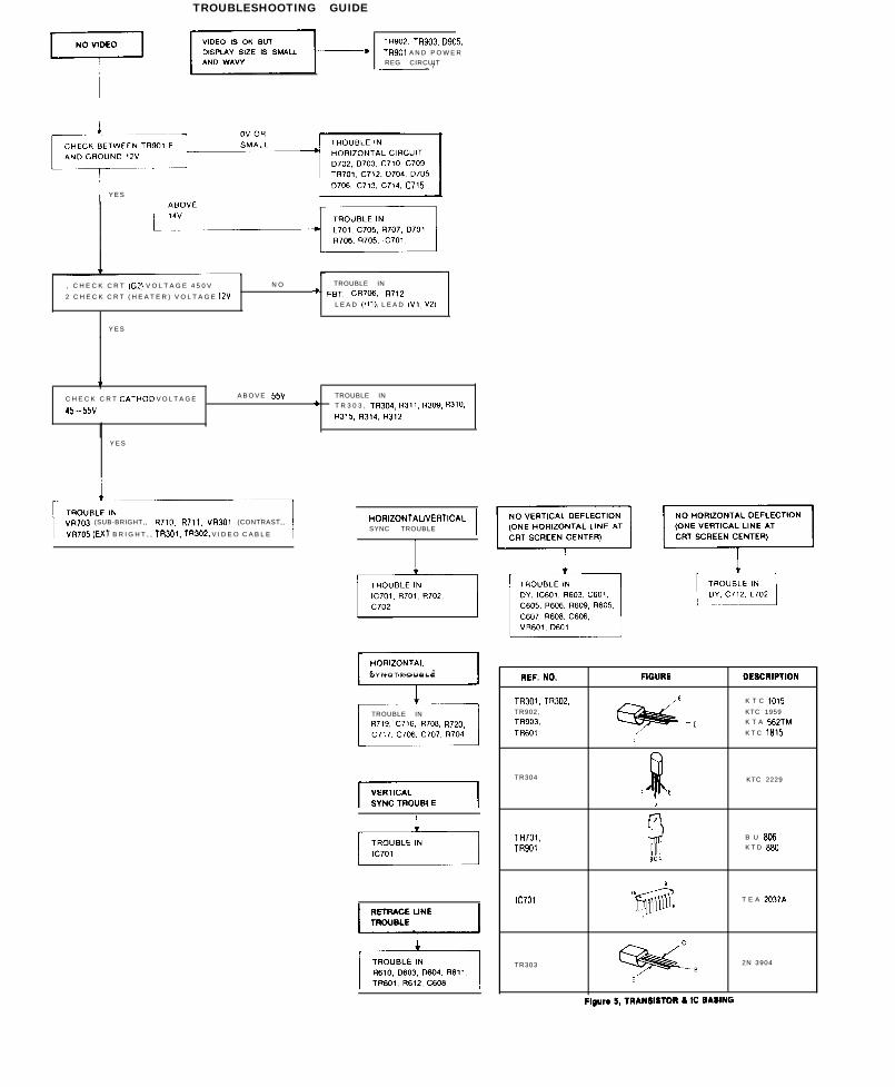
TROUBLESHOOTING GUIDE
TR902, TR903. D905.
TR901 A N D P O W E RREG CIRCUIT~. 7
I D706, c713. c714. c715Y E S
, C H E C K C R T (GZ) V O L T A G E 4 5 0 V N O TROUBLE IN
2 C H E C K C R T ( H E A T E R ) V O L T A G E 12V -, FBT. CR706 R712L E A D (HI,. L E A D (Vl, V2)
Y E S
C H E C K C R T CATHOD V O L T A G E A B O V E 55V TROUBLE IN*
45-55vT R 3 0 3 , TR304. R311. R309. R310.
R315, R314, R312
Y E S
VR703 (SUB-BRIGHT,, R710. R711. “R301 (CONTRAST,,
VI?,05 (MT B R I G H T , , TRW, TR302. V I D E O C A B L E
HORIZONTAWERTICAL
SYNC TROUBLE I
S Y N C T R O U B L E
TROUBLE IN
R719. C716. R70B, R720.
I
I
REF. NO. FIGURE OEBCRIPTION
TR301. TR302. B
w
K T C ,015
TR902, KTC 1959
TR903. -C K T A 562TM
TR601 K T C 1815L
TR304
k
KTC 2229
t B
c
>
TR701.
9
B U 806
TWO1 K T D 880
BCE
IC701l@a
T E A 2037A
TR303-0
2N 3904
E
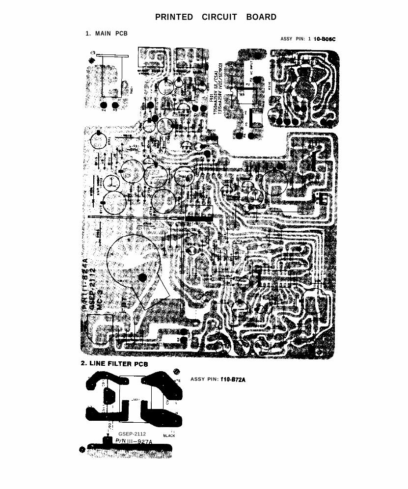
PRINTED CIRCUIT BOARD
1. MAIN PCBASSY PIN: 1 lo-BOW
ASSY PIN: ilO-B72A
J GSEP-2112 TIBLACK
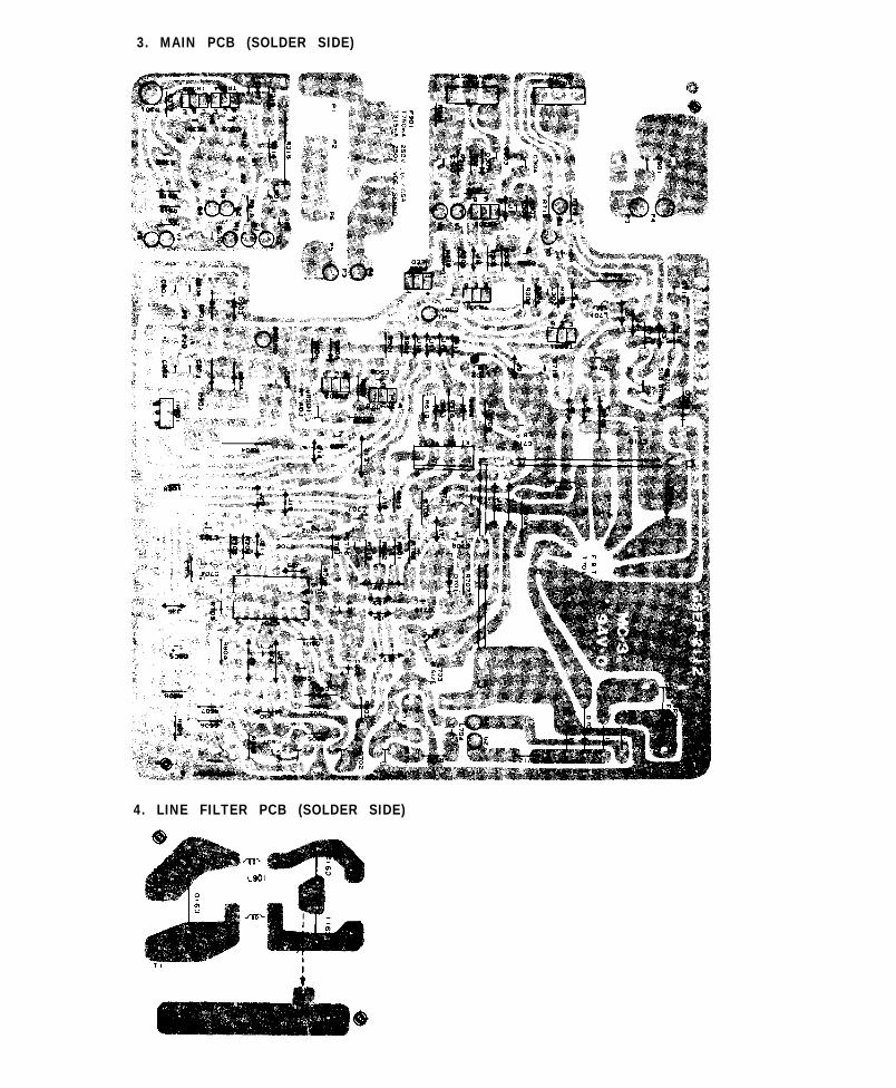
3. MAIN PCB (SOLDER SIDE)
4. LINE FILTER PCB (SOLDER SIDE)
O-0
Lsol
I
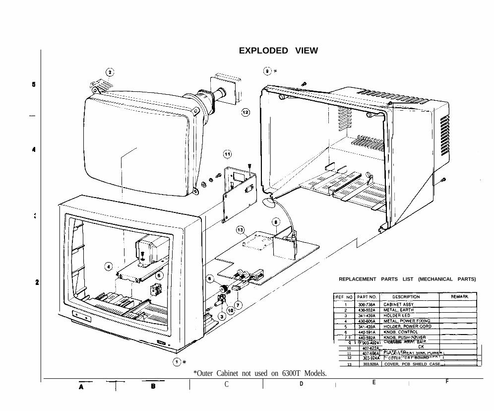
EXPLODED VIEW
REPLACEMENT PARTS LIST (MECHANICAL PARTS)
8 , 1ILr.I w
9 1 3X3-A02A 1 COVER ASSY. B&___ .-10 407-622A11 407.696A , I-LAIE., “x-t WNR ruvvcn,12 303.924A 1 COVER, C R T BOARD I
13 303.928A [ COVER, PCB SHIELD CASE 1
*Outer Cabinet not used on 6300T Models.C D I E I F
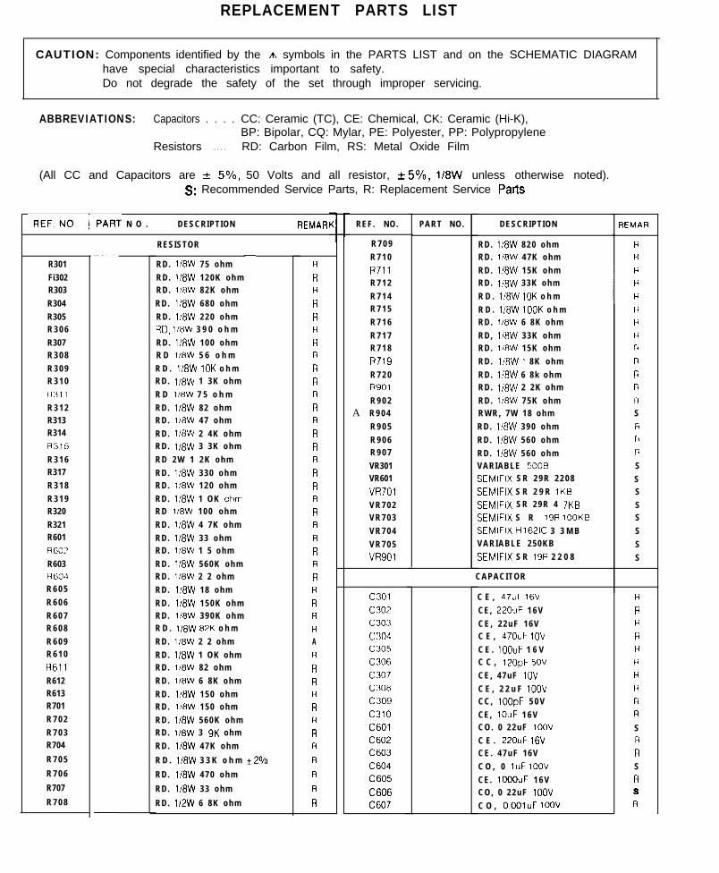
REPLACEMENT PARTS LIST
CAUTION: Components identified by the A symbols in the PARTS LIST and on the SCHEMATIC DIAGRAMhave special characteristics important to safety.Do not degrade the safety of the set through improper servicing.
ABBREVIATIONS: Capacitors . . . . CC: Ceramic (TC), CE: Chemical, CK: Ceramic (Hi-K),BP: Bipolar, CQ: Mylar, PE: Polyester, PP: Polypropylene
Resistors . . . . RD: Carbon Film, RS: Metal Oxide Film
(All CC and Capacitors are + 5%, 50 Volts and all resistor, +5%, 118W unless otherwise noted).S: Recommended Service Parts, R: Replacement Service PatIS
REF.NO.]PART N O . 1 DESCRIPTION REMAR
R301
Fi302
R303
R304
R305
R 3 0 6
R307
R 3 0 8
R 3 0 9
R 3 1 0
R311
R 3 1 2
R313
R314
R315
R 3 1 6
R317
R 3 1 8
R 3 1 9
R320
R321
R601
R602
R603
R604
R 6 0 5
R 6 0 6
R 6 0 7
R 6 0 8
R 6 0 9
R 6 1 0
R611
R612
R613
R701
R 7 0 2
R 7 0 3
R704
R 7 0 5
R 7 0 6
R707
R 7 0 8
RESISTOR
RD. 118W 75 ohm
RD. 118W 1 2 0 K o h m
RD. 118W 82K ohm
RD. 118W 6 8 0 o h m
RD. 118W 2 2 0 o h m
RD, 118W 3 9 0 o h m
RD. 118W 1 0 0 o h m
R D 118W 5 6 o h m
R D . 1/8W 10K o h m
RD. 118W 1 3K ohm
R D 118W 7 5 o h m
RD. 118W 82 ohm
RD. 118W 47 ohm
RD. 1/8W 2 4K ohm
RD. 118W 3 3K ohm
R D 2 W 1 2 K o h m
RD. l/SW 3 3 0 o h m
RD. l/SW 1 2 0 o h m
RD. 118W 1 OK ohm
RD 118W 1 0 0 o h m
RD. 118W 4 7K ohm
RD. 118W 33 ohm
RD. 118W 1 5 ohm
RD. 118W 5 6 0 K o h m
RD. 118W 2 2 ohm
RD. 118W 18 ohm
RD. l/SW 1 5 0 K o h m
RD. 118W 3 9 0 K o h m
R D . 1/8W 82K o h m
RD. 118W 2 2 ohm
RD. 118W 1 OK ohm
RD. 118W 82 ohm
RD. 118W 6 8K ohm
RD. 118W 1 5 0 o h m
RD. 118W 1 5 0 o h m
RD. ll8W 5 6 0 K o h m
RD. 118W 3 9K ohm
RD. 118W 47K ohm
R D . 118W 3 3 K o h m +20/o
RD. 118W 4 7 0 o h m
RD. 118W 33 ohm
RD. 112W 6 8K ohm
R
R
R
R
R
R
R
R
R
R
R
R
R
R
R
R
R
R
R
R
R
R
R
R
R
R
R
R
R
A
R
R
R
R
R
R
R
R
R
R
R
R
REF. NO. PART NO. DESCRIPTION
R 7 0 9 RD. 118W 8 2 0 o h m
R 7 1 0 RD. 1/8W 47K ohm
R711 RD. 118W 15K ohm
R 7 1 2 RD. 118W 33K ohm
R 7 1 4 R D . 118W 10K o h m
R 7 1 5 R D . 118W IOOK o h m
R 7 1 6 RD. 118W 6 8K ohm
R 7 1 7 RD, 118W 33K ohm
R 7 1 8 RD. li8W 15K ohm
R719 RD. 118W 1 8K ohm
R 7 2 0 RD. 118W 6 8 k o h m
R901 RD. 1/8W 2 2K ohm
R 9 0 2 RD. 1/8W 75K ohm
A R 9 0 4 RWR, 7W 18 ohm
R 9 0 5 RD. 118W 3 9 0 o h m
R 9 0 6 RD. 118W 5 6 0 o h m
R 9 0 7 RD. 118W 5 6 0 o h m
VR301 VARIABLE 5008
VR601 SEMIFIX S R 2 9 R 2 2 0 8
VR701 SEMIFIX S R 2 9 R 1KB
V R 7 0 2 SEMIFIX S R 2 9 R 4 7KB
V R 7 0 3 SEMIFIX S R 19R 1OOKB
V R 7 0 4 SEMIFIX H162lC 3 3 M B
V R 7 0 5 VARIABLE 250KB
VR901 SEMIFIX S R 19R 2 2 0 8
CAPACITOR
c301
C302
c303
c304
c305
C306
c307
C308
c309
c310
C601
C602
C603
C604
C605
C606
C607
C E , 47uF 16V
CE, 22OuF 1 6 V
C E , 2 2 u F 1 6 V
C E , 47OuF IOV
C E . 1OOuF 1 6 V
C C , 12OpF 5OV
CE, 47uF 1OV
C E , 2 2 u F IOOV
CC, IOOpF 5 0 V
CE, IOuF 1 6 V
CO. 0 22uF IOOV
C E . 22OuF 16V
C E . 4 7 u F 1 6 V
C O , 0 IuF IOOV
CE. 1OOOuF 1 6 V
CO, 0 22uF 1OOV
C O , OOOluF 1OOV
3EMARl
R
w
R
R
R
R
R
R
R
R
R
R
H
S
R
F i
R
S
S
S
S
S
S
S
S
R
R
R
R
R
R
R
R
R
R
SR
R
S
R
s
R
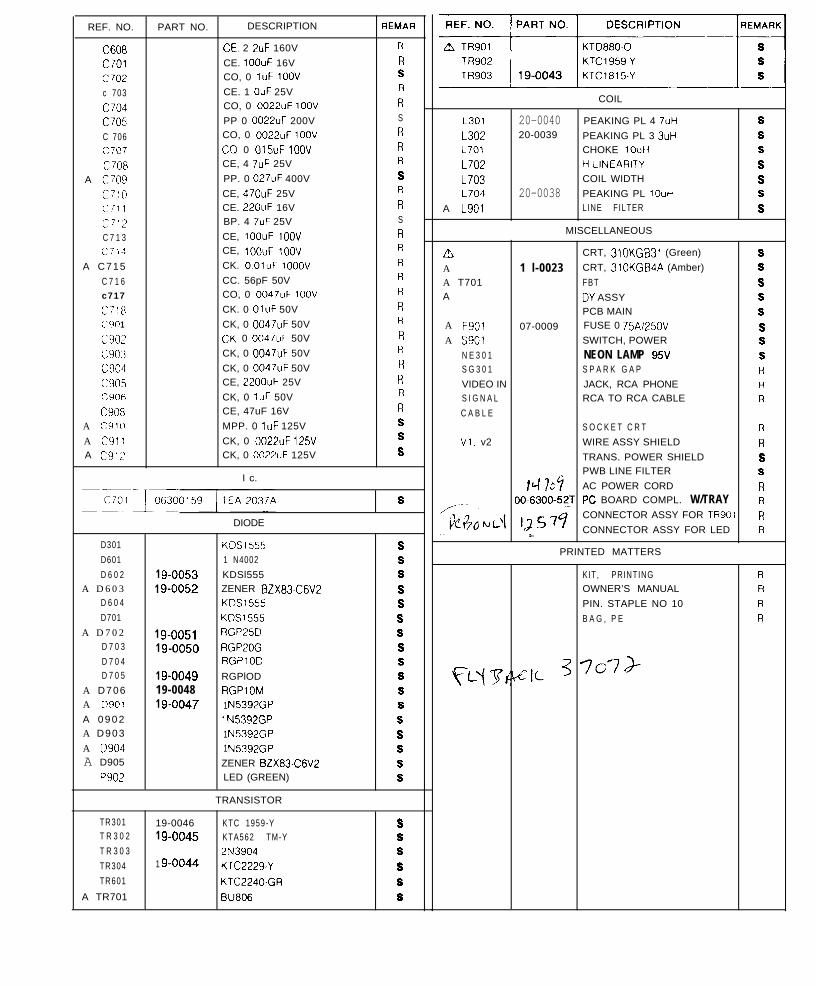
REF. NO. PART NO. DESCRIPTION REMAR
C608 CE. 2 2uF 160V R
c701 CE. 1OOuF 16V R
C702 CO, 0 1uF 1OOV s
c 703 CE. 1 OuF 25V R
c704 CO, 0 0022uF 1OOV R
c705 PP 0 0022uF 200V S
C 706 CO, 0 0022uF 1OOV R
c707 CQ. 0 015uF 1OOV R
C708 CE, 4 7uF 25V R
A C709 PP. 0 027uF 400V s
CT10 CE, 47OuF 25V R
(1711 CE. 22OuF 16V R
c’712 BP. 4 7uF 25V S
C 7 1 3 CE, IOOuF IOOV R
c714 CE, 1OOuF 1OOV R
A C715 CK. OOluF 1OOOV R
C 7 1 6 CC. 56pF 50V R
c717 CO, 0 0047uF IOOV R
c-718 CK. 0 OluF 50V R
c90 1 CK, 0 0047uF 50V R
cc)02 CK, 0 0047uF 50V R
c903 CK, 0 0047uF 50V R
c904 CK, 0 0047uF 50V R
c905 CE, 22OOuF 25V R
C906 CK, 0 1uF 50V R
C908 CE, 47uF 16V R
A c91o MPP. 0 1uF 125V S
A C911 CK, 0 0022uF 125V S
A c912 CK, 0 0022uF 125V S
I c.
S
DIODE
D301 KDSl555 SD601 1 N4002 SD 6 0 2 1 g-0053 KDSl555 S
A D603 1 g-0052 ZENER 62x83.C6V2 SD 6 0 4 KDSl555 SD701 KDSl555 S
A D702 1 g-0051 RGP25D SD 7 0 3 1 g-0050 RGPZOG SD 7 0 4 RGPlOD SD 7 0 5 1 g-0049 RGPlOD S
A D706 19-0048 RGPlOM SA D901 1 g-0047 1 N5392GP SA 0 9 0 2 1 N5392GP SA D903 1 N5392GP SA 0904 1 N5392GP SA D905 ZENER BZX83-C6V2 S
P902 LED (GREEN) S
TRANSISTOR
TR301 19-0046 KTC 1959-Y ST R 3 0 2 1 g-0045 KTA562 TM-Y ST R 3 0 3 2N3904 STR304 1 g-0044 KTC2229-Y STR601 KTC2240.GR S
A TR701 BU806 S
COIL
L301 20-0040 PEAKING PL 4 7uH SL302 20-0039 PEAKING PL 3 3uH SL701 CHOKE IOuH SL702 H~LINEARITY SL703 COIL WIDTH SL704 20-0038 PEAKING PL 1OuH S
A L901 LINE FILTER S
MISCELLANEOUS
Q CRT, 310KG531 (Green) SA 1 l-0023 CRT, 310KGB4A (Amber) SA T701 FBT SA DY ASSY S
PCB MAIN SA F901 07-0009 FUSE 0 75Ai250V SA S901 SWITCH, POWER S
N E 3 0 1 NEON LAMP 95V SS G 3 0 1 S P A R K G A P RVIDEO IN JACK, RCA PHONE RS I G N A L RCA TO RCA CABLE RC A B L E
S O C K E T C R T RVl. v2 WIRE ASSY SHIELD R
TRANS. POWER SHIELD SPWB LINE FILTER
fd IcyS
AC POWER CORD R
“j&c hl c\l
OO-6300-5?T PC BOARD COMPL. W/TRAY R
t,> s 77CONNECTOR ASSY FOR TR901 R
. . CONNECTOR ASSY FOR LED R-
PRINTED MATTERS
KIT, PRINTING ROWNER’S MANUAL RPIN. STAPLE NO 10 RB A G , P E R
3 77-7 J-


