Graded-index Polymer Multimode Waveguides for 100 Gb/s Board-level Data Transmission Jian Chen 1 , Nikos Bamiedakis 1 , Peter Vasil'ev 1 , Tom J. Edwards 2 , Tom Brown 2 , Richard V. Penty 1 , Ian H. White 1 1 Electrical Engineering Division, University of Cambridge, UK e-mail: [email protected]2 SUPA, School of Physics & Astronomy, University of St Andrews, UK European Conference on Optical Communication (ECOC 2015) 28th September 2015
Transcript
Graded-index Polymer Multimode Waveguides for
100 Gb/s Board-level Data Transmission
Jian Chen1, Nikos Bamiedakis1, Peter Vasil'ev1, Tom J. Edwards2, Tom Brown2,
Richard V. Penty1, Ian H. White1
1Electrical Engineering Division, University of Cambridge, UK
2SUPA, School of Physics & Astronomy, University of St Andrews, UK
European Conference on Optical Communication (ECOC 2015)
28th September 2015
Outline
• Introduction to Optical Interconnects
• Board-level Optical Interconnects
• Bandwidth Studies
Experimental Results
Waveguide Modelling
• Conclusions
Outline
• Introduction to Optical Interconnects
• Board-level Optical Interconnects
• Bandwidth Studies
Experimental Results
Waveguide Modelling
• Conclusions
Why Optical Interconnects?
Growing demand for data communications link capacity in:
- data centres
- supercomputers
need for high-capacity short-reach interconnects operating at > 25 Gb/s
Optics better than copper at high data rates (bandwidth, power, EMI, density)
E.Varvarigos, Summer School on Optical Interconnects, 2014.K. Hiramoto, ECOC 2013.
Outline
• Introduction to Optical Interconnects
• Board-level Optical Interconnects
• Bandwidth Studies
Waveguide Modelling
Experimental Results
• Conclusions
Board-level Optical Interconnects
• Various approaches proposed:
free space interconnects
fibres embedded in substrates
waveguide-based technologies
M. Schneider, et al., ECTC 2009.
Jarczynski J. et al., Appl. Opt, 2006.R. Dangel, et al., JLT 2013.
Siloxane
waveguidesInterconnection
architectures
Board-level OE
integration PCB-integrated
optical units
Basic waveguide
components
Our work:
Polymer waveguides
Polymer Multimode Waveguides
- Siloxane Polymer Materials
• low intrinsic attenuation (0.03–0.05 dB/cm at 850 nm);
• good thermal and mechanical properties (up to 350 °C);
• low birefringence;
• fabricated on FR4, glass or silicon using standard techniques
• offer refractive index tunability
- Multimode Waveguide
• Cost-efficiency: relaxed alignment tolerances
assembly possible with pick-and-place machines
50 μm core
top cladding
bottom cladding
Substrate
suitable for integration on PCBs
offer high manufacturability
are cost effective
- typical cross section used: 50×50 μm2
- 1 dB alignment tolerances: > ± 10 μm
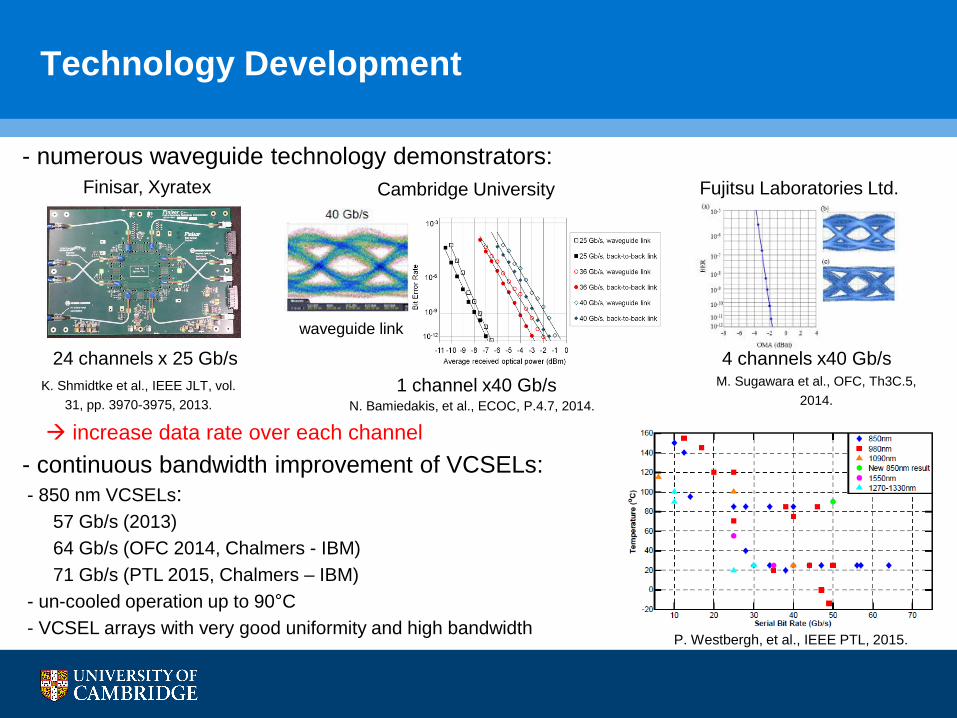
Technology Development
increase data rate over each channel
N. Bamiedakis, et al., ECOC, P.4.7, 2014.
waveguide link
Finisar, Xyratex
24 channels x 25 Gb/s
K. Shmidtke et al., IEEE JLT, vol.
31, pp. 3970-3975, 2013.
4 channels x40 Gb/sM. Sugawara et al., OFC, Th3C.5,
2014.
Fujitsu Laboratories Ltd.
1 channel x40 Gb/s
Cambridge University
- numerous waveguide technology demonstrators:
- continuous bandwidth improvement of VCSELs:
- 850 nm VCSELs:
57 Gb/s (2013)
64 Gb/s (OFC 2014, Chalmers - IBM)
71 Gb/s (PTL 2015, Chalmers – IBM)
- un-cooled operation up to 90°C
- VCSEL arrays with very good uniformity and high bandwidth P. Westbergh, et al., IEEE PTL, 2015.
Demand for Higher Bandwidth
their highly-multimoded nature raises important concerns about their bandwidth
limitations and their potential to support very high on-board data rates (e.g. >100 Gb/s)?
23 GHz (BLP1: 57.5 GHz×m) for a 2.55 m long waveguide2
150 GHz (BLP1: 75 GHz×m) for a 51 cm long waveguide3
1.03 GHz (BLP1: 90 GHz×m) for a 90 m long waveguide4
SI:
GI:
Examples:Restricted centre
launch
Effects of launch conditions & input offsets?
2F. Doany, et al., LEOS Summer Topical Meetings, 2004.3X. Wang, et al., Optics letters, vol. 32, no. 6, pp. 677–679, 2007.4T. Kosugi , et al., Optics express, vol. 17, no. 18, pp. 15959–15968, 2009.
BLP1: Bandwidth-length product.
- step-index (SI) vs. graded-index (GI) waveguides
achieve higher bandwidth: renewed interest on ultimate dispersion limits
T. Ishigure, Summer
School on Optical
Interconnects, 2014.
Outline
• Introduction to Optical Interconnects
• Board-level Optical Interconnects
• Bandwidth Studies
Experimental Results
Waveguide Modelling
• Conclusions
x (m)
y (
m)
-25-20-15-10 -5 0 5 10 15 20 25-25
-20
-15
-10
-5
0
5
10
15
20
25
1.516
1.518
1.52
1.522
1.524
1 m Graded-index (GI) Spiral Multimode Waveguide
- It is described as “GI” here, although it does not have the parabolic GI profile as typically
encountered in MMFs.
this particular feature is due to fabrication process and the mechanism is under study.
(a) the 1 m long spiral waveguide
illuminated with red light
(a)
Brandon W. Swatowski, et al., IEEE Optical Interconnects Conference
(OIC 2014), WD2, 2014.
- 1 m long multimode spiral waveguide
- cross section 32×36 µm2, ∆n ~ 0.01
- sample fabricated on 8’’ inch Si substrate
- input/output facets exposed with dicing saw
- no polishing steps undertaken
(b) Measured RI profile of the
waveguide at 678 nm
(b)
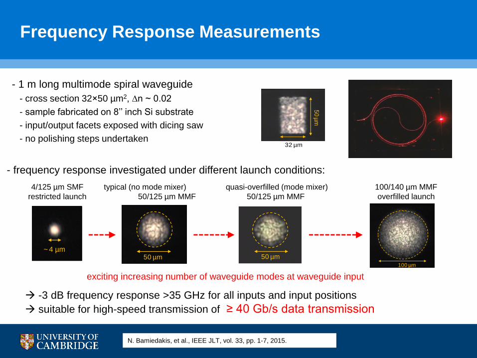
Frequency Response Measurements
-3 dB frequency response >35 GHz for all inputs and input positions
suitable for high-speed transmission of ≥ 40 Gb/s data transmission
N. Bamiedakis, et al., IEEE JLT, vol. 33, pp. 1-7, 2015.
- 1 m long multimode spiral waveguide
- cross section 32×50 µm2, ∆n ~ 0.02
- sample fabricated on 8’’ inch Si substrate
- input/output facets exposed with dicing saw
- no polishing steps undertaken32 µm
50
µm
- frequency response investigated under different launch conditions:
~ 4 µm 50 µm 50 µm
100 µm
exciting increasing number of waveguide modes at waveguide input
4/125 µm SMF
restricted launch
typical (no mode mixer)
50/125 µm MMF
quasi-overfilled (mode mixer)
50/125 µm MMF
100/140 µm MMF
overfilled launch
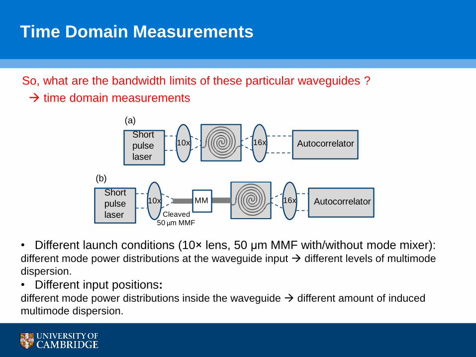
Time Domain Measurements
• Different launch conditions (10× lens, 50 μm MMF with/without mode mixer): different mode power distributions at the waveguide input different levels of multimode
dispersion.
• Different input positions: different mode power distributions inside the waveguide different amount of induced
multimode dispersion.
So, what are the bandwidth limits of these particular waveguides ?
time domain measurements
Short
pulse
laser
Autocorrelator10x 16x
Cleaved 50 μm MMF
Short
pulse
laser
Autocorrelator10x 16x
(a)
(b)
MM
∆tin∆tout
Input pulse Output pulse1. Two short pulse generation systems
(a) Ti:Sapphire laser emitting at 850 nm
(b) Femtosecond erbium-doped fibre laser at ~1574 nm
and a frequency-doubling crystal to generate pulses
at wavelength of ~787 nm
2. Matching autocorrelator to record output pulse
3. Convert autocorrelation traces back to pulse traces
curve fitting is needed to determine the shapes of the original pulses, i.e. Gaussian, sech2
or Lorentzian.
4. Bandwidth calculation
waveguide frequency response and bandwidth estimated by comparing Fourier
Transforms of input and output pulses
Bandwidth Estimation
allow more detailed study with a range of launch conditions


![Research Article The Spiral Coaxial Cable · 2019. 7. 31. · ], and the channel waveguides (buried, strip-loaded, ridge, rib, di used, and graded-dielectric index [ ]). e two-wire](https://static.documents.pub/doc/80x56/612774de2755fa40d303f1b1/research-article-the-spiral-coaxial-cable-2019-7-31-and-the-channel-waveguides.jpg)
