32

Limits of Scaling MOSFETs
Grant McFarland and Michael Flynn
Technical Report CSL-TR-95-662
January 1995
This work was supported by the NSF under contract MIP93-13701 and by
fellowship support from the IBM/CIS Fellow Mentor Advisor Program.

Limits of Scaling MOSFETs
by
Grant McFarland and Michael Flynn
Technical Report CSL-TR-95-662
January 1995
Computer Systems Laboratory
Departments of Electrical Engineering and Computer Science
Stanford University
Stanford, California 94305-4055
Abstract
The fundamental electrical limits of MOSFETs are discussed and modeled to predict the scaling
limits of digital bulk CMOS circuits. Limits discussed include subthreshold currents, time depen-
dent dielectric breakdown (TDDB), hot electron e�ects, and drain induced barrier lowering (DIBL).
This paper predicts the scaling of bulk CMOS MOSFETs to reach its limits at drawn dimensions
of approximately 0:1�m. These electrical limits are used to �nd scaling factors for SPICE Level
3 model parameters, and a scalable Level 3 device model is presented. Current trends in scaling
interconnects are also discussed.
Key Words and Phrases: MOSFET, device scaling, interconnect scaling, time dependent
dielectric breakdown, hot electron e�ects, drain induced barrier lowering, spice models

Copyright c 1995
by
Grant McFarland and Michael Flynn

Contents
1 Constant Field Scaling 1
2 Performance Scaling 2
2.1 Subthreshold Leakage Currents : : : : : : : : : : : : : : : : : : : : : : : : : : : : : : 3
2.2 Time Dependent Dielectric Breakdown (TDDB) : : : : : : : : : : : : : : : : : : : : 4
2.3 Hot Electron E�ects : : : : : : : : : : : : : : : : : : : : : : : : : : : : : : : : : : : : 4
2.4 Short Channel E�ects : : : : : : : : : : : : : : : : : : : : : : : : : : : : : : : : : : : 8
2.5 Summary of Scaling Limits : : : : : : : : : : : : : : : : : : : : : : : : : : : : : : : : 10
2.6 Performance Scaling of SPICE Level 3 Model : : : : : : : : : : : : : : : : : : : : : : 11
3 Delay of Scaled Devices 12
4 Scaling of Interconnects 12
5 Conclusions 14
Appendix A { SIA Roadmap 16
Appendix B { Scalable HSPICE Device Models 17
Appendix C { Scalable HSPICE Wire Models 18
Appendix D { Mathematica Models 20
TOXBREAK : : : : : : : : : : : : : : : : : : : : : : : : : : : : : : : : : : : : : : : : : : : 20
LEFF : : : : : : : : : : : : : : : : : : : : : : : : : : : : : : : : : : : : : : : : : : : : : : : 21
NSUBMIN : : : : : : : : : : : : : : : : : : : : : : : : : : : : : : : : : : : : : : : : : : : : 22
WIREDELAY : : : : : : : : : : : : : : : : : : : : : : : : : : : : : : : : : : : : : : : : : : 23
RULES : : : : : : : : : : : : : : : : : : : : : : : : : : : : : : : : : : : : : : : : : : : : : : 24
iii

List of Figures
1 Fanout of 4 Inverter Delay : : : : : : : : : : : : : : : : : : : : : : : : : : : : : : : : : 3
2 Gate Oxide Fields vs Year : : : : : : : : : : : : : : : : : : : : : : : : : : : : : : : : : 5
3 Minimum Gate Oxide Thickness : : : : : : : : : : : : : : : : : : : : : : : : : : : : : 5
4 Channel Fields vs Year : : : : : : : : : : : : : : : : : : : : : : : : : : : : : : : : : : : 7
5 Minimum LEFF : : : : : : : : : : : : : : : : : : : : : : : : : : : : : : : : : : : : : : 7
6 Drain Induced Barrier Lowering : : : : : : : : : : : : : : : : : : : : : : : : : : : : : : 9
7 Minimum Channel Doping : : : : : : : : : : : : : : : : : : : : : : : : : : : : : : : : : 9
8 Fanout of 4 Inverter Delay : : : : : : : : : : : : : : : : : : : : : : : : : : : : : : : : : 12
9 Wire Delay : : : : : : : : : : : : : : : : : : : : : : : : : : : : : : : : : : : : : : : : : 14
iv
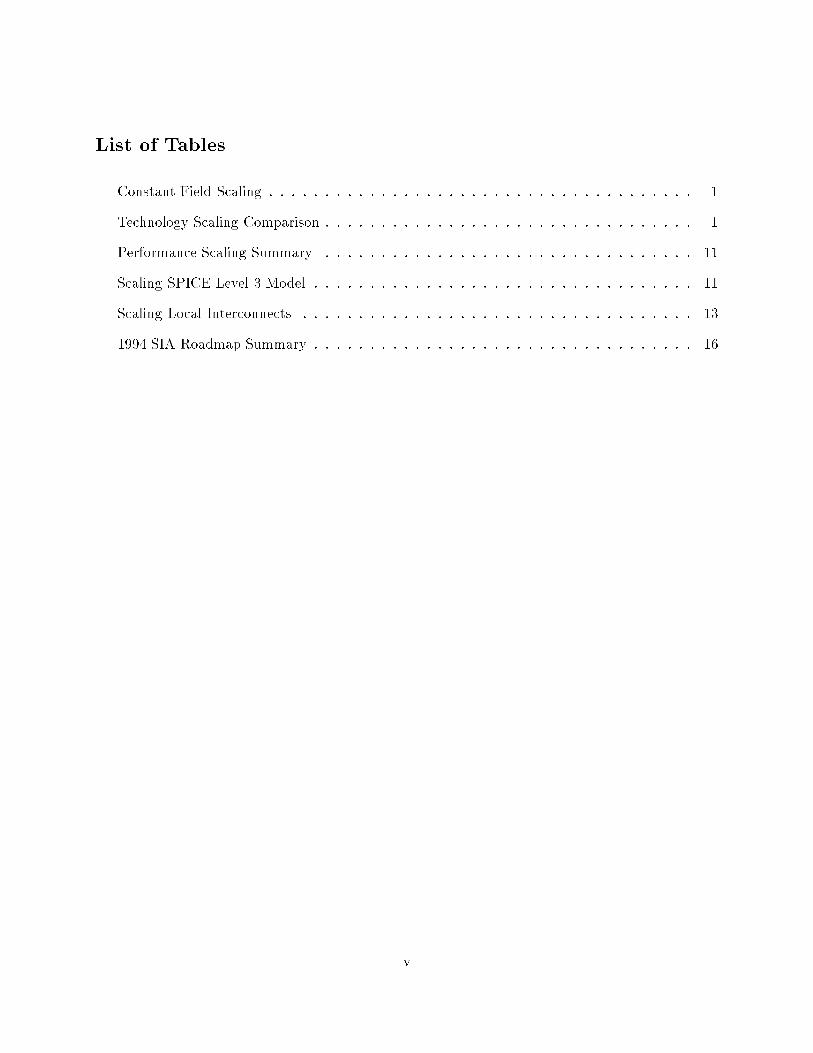
List of Tables
Constant Field Scaling : : : : : : : : : : : : : : : : : : : : : : : : : : : : : : : : : : : : : : 1
Technology Scaling Comparison : : : : : : : : : : : : : : : : : : : : : : : : : : : : : : : : : 1
Performance Scaling Summary : : : : : : : : : : : : : : : : : : : : : : : : : : : : : : : : : 11
Scaling SPICE Level 3 Model : : : : : : : : : : : : : : : : : : : : : : : : : : : : : : : : : : 11
Scaling Local Interconnects : : : : : : : : : : : : : : : : : : : : : : : : : : : : : : : : : : : 13
1994 SIA Roadmap Summary : : : : : : : : : : : : : : : : : : : : : : : : : : : : : : : : : : 16
v
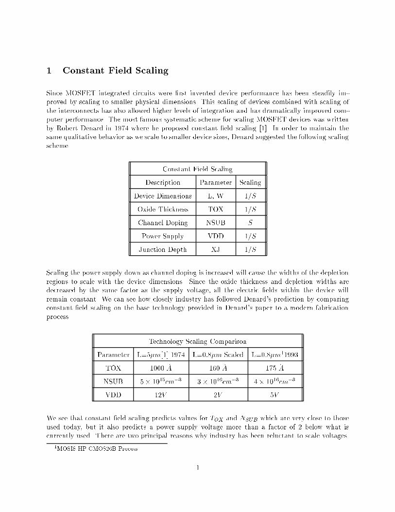
1 Constant Field Scaling
Since MOSFET integrated circuits were �rst invented device performance has been steadily im-
proved by scaling to smaller physical dimensions. This scaling of devices combined with scaling of
the interconnects has also allowed higher levels of integration and has dramatically improved com-
puter performance. The most famous systematic scheme for scaling MOSFET devices was written
by Robert Denard in 1974 where he proposed constant �eld scaling [1]. In order to maintain the
same qualitative behavior as we scale to smaller device sizes, Denard suggested the following scaling
scheme.
Constant Field Scaling
Description Parameter Scaling
Device Dimensions L, W 1=S
Oxide Thickness TOX 1=S
Channel Doping NSUB S
Power Supply VDD 1=S
Junction Depth XJ 1=S
Scaling the power supply down as channel doping is increased will cause the widths of the depletion
regions to scale with the device dimensions. Since the oxide thickness and depletion widths are
decreased by the same factor as the supply voltage, all the electric �elds within the device will
remain constant. We can see how closely industry has followed Denard's prediction by comparing
constant �eld scaling on the base technology provided in Denard's paper to a modern fabrication
process.
Technology Scaling Comparison
Parameter L=5�m[1] 1974 L=0:8�m Scaled L=0:8�m11993
TOX 1000 �A 160 �A 175 �A
NSUB 5� 1015cm�3 3� 1016cm�3 4� 1016cm�3
VDD 12V 2V 5V
We see that constant �eld scaling predicts values for TOX and NSUB which are very close to those
used today, but it also predicts a power supply voltage more than a factor of 2 below what is
currently used. There are two principal reasons why industry has been reluctant to scale voltages.
1MOSIS HP CMOS26B Process
1

The �rst is the di�culties caused in board level design for chips designed to operate at di�erent
voltages. Secondly scaling the power supply hurts performance. This has caused chip foundries to
avoid scaling power supplies as long as possible, and therefore while constant �eld scaling has been
a good predictor of oxide thicknesses and doping levels, it has not been a good predictor of power
supply voltages or device performance. Other criteria besides constant �elds are needed to predict
future scaling of devices.
2 Performance Scaling
Performance scaling seeks to scale each fabrication parameter to provide the highest performance
device possible. The fact that current power supplies are much higher than predicted by Denard
shows that the industry as a whole is not interested in maintaining constant �elds. More realistic
motivations for scaling device parameters are performance and reliability. Therefore, to predict
the scaling of future technologies we should scale each parameter to provide the highest perfor-
mance device possible while satisfying certain basic electrical and reliability requirements. These
fundamental limits include the following:
Subthreshold Leakage Currents
To keep power consumption down we must limit leakage currents by maintaining reasonably
high thresholds. For high performance operation the power supply voltage must be signi�-
cantly above the threshold. These requirements of low leakage and high performance limit
how small a power supply voltage may be used.
Time Dependent Dielectric Breakdown
High electric �elds in the gate oxide can cause gradual deterioration of the oxide layer until
eventually dielectric breakdown is reached. Long term reliability of the gate oxide limits how
thin an oxide layer may be used.
Hot Electron E�ects
High lateral �elds in the channel can accelerate some electrons to high enough energies to
pass into the gate oxide and change the device threshold over time. Long term threshold
stability limits how short a channel length may be used.
Short Channel E�ects
As we move the source and drain of a MOSFET closer physically together, it becomes more
and more di�cult to electrically isolate them. In deep sub-micron MOSFETs the depletion
regions of the source and drain can signi�cantly deplete the channel region making the thresh-
old a function of the device length and drain voltage. These e�ects limit how low a doping
concentration may be used.
In the following sections we will examine the nature of these limitations and how they e�ect the
scaling of MOSFETs.
2

2.1 Subthreshold Leakage Currents
Simple MOSFET models assume that the device current is 0 for Vgs < VT , however in reality the
drain current decreases exponentially to 0 as the gate voltage drops below the threshold. The slope
of this subthreshold current can be shown to be:
d(Vgs)
d(logID)= (
kT
qln 10)(1 +
CD
COX) (1)
Where CD is the depletion capacitance in the channel. This means that at room temperature in
the best case where CD � COX the subthreshold slope will be:
d(Vgs)
d(logID)= 60mV=decade (2)
The on/o� current ratio of a device is de�ned as the ratio of the current at VGS = VT and the
current at VGS = 0. The larger this ratio the less signi�cant leakage currents will be for a particular
technology. For high performance chips we assume a current ratio of at least 105 is desirable [2],
which assuming optimum subthreshold slope gives a minimum VT > 0:3V .
Because currents drop o� exponentially in the subthreshold regime, circuits designed to switch
using primarily subthreshold currents will face severe performance penalties (see �gure 1).
|1.0
|1.5
|2.0
|2.5
|3.0
|3.5
|4.0
|4.5
|5.0
|0.0
|0.2
|0.4
|0.6
|0.8
|1.0
Vdd/Vt
Del
ay
Figure 1: Fanout of 4 Inverter Delay
For high performance operation we must use a power supply voltage su�ciently greater than VTso that devices will spend most of their switching time out of the subthreshold regime. Analyzing
3

performance as a function of VT=VDD shows that a good requirement for high performance operation
is [3]:
VDD > 4VT > 1:2V (3)
Therefore, subthreshold currents and the need for high performance limit the extent to which we
can scale VDD and VT .
2.2 Time Dependent Dielectric Breakdown (TDDB)
MOSFET current drive can be increased and short channel e�ects reduced by using thinner gate
oxides. However, if the power supply voltage is not scaled with the oxide thickness, �elds in the
oxide will increase. Experiments have shown that over time these high �elds can damage the oxide
layer until eventually breakdown occurs [4]. The time to breakdown is commonly written as:
tBD = �0 expG=EOX (4)
where G is the breakdown acceleration factor, �0 is a time constant, and EOX is the �eld in the
oxide. At 25�C typical values for G and �0 are 350MV=cm and 1� 10�11 sec [5]. At 125�C tBD is
seen to be reduced by a factor of 20 compared to lifetimes at 25�C [6]. By solving for the electric
�eld we are able to �nd that in order to have a 10 year lifetime at 125�C the �eld in the gate oxide
should be below approximately 7MV=cm. Assuming a worst case voltage of 10% over the nominal
supply and adding 50% to the minimum thickness in order to compensate for process variation and
defects we calculate the following condition:
TOX > 1:5(1:1VDD)=(7MV=cm) (5)
EOX = VDD=TOX < 4:24MV=cm (6)
Keeping this limit in mind we can look at how the gate oxide �elds of SRAMs and processors
have changed in recent years. Figure 2 shows that �elds in the gate oxide have been steadily
increasing until today dielectric breakdown is a serious concern, and it is common to �nd parts
with �elds very close to the limit we have given. Figure 3 compares this limitation with the oxide
thicknesses projected in the SIA Roadmap [7] and shows that this restriction should be valid for
future MOSFET generations as well.
2.3 Hot Electron E�ects
Another e�ect of not scaling power supply voltages with device size has been increasing lateral
electric �elds in the channel. At su�ciently high �elds electrons may gain enough energy to over
come the oxide barrier and enter the gate oxide. This build up of negative charge will causes NMOS
thresholds to increase over time. Eventually reduced current drive will cause the circuit to fail.
PMOS devices can also experience hot electron e�ects. In high �elds holes can cause impact
ionization in the channel producing an electron-hole pair. This free electron can then be swept
4

� Vdd = 5.0V Vdd = 3.3V� Vdd = 2.5V
|80
|82
|84
|86
|88
|90
|92
|94
|1
|2
|3
|4
|5
Year
EO
X (
MV
/cm
)
SiO2 Breakdown Limit
�
�
�
�
���
����
��
�
�
�
�
�
�
�
�
�
�
�
���
�
�
�
�
��
��
�
�
�
Figure 2: Gate Oxide Fields vs Year
� SIA Roadmap 10 year TDDB
|1.0
|1.5
|2.0
|2.5
|3.0
|3.5
|0
|12
|25
|38
|50
|62
|75
|88
|100
Vdd (V)
Tox
(A
A)
�
�
�
�
�
Figure 3: Minimum Gate Oxide Thickness
5
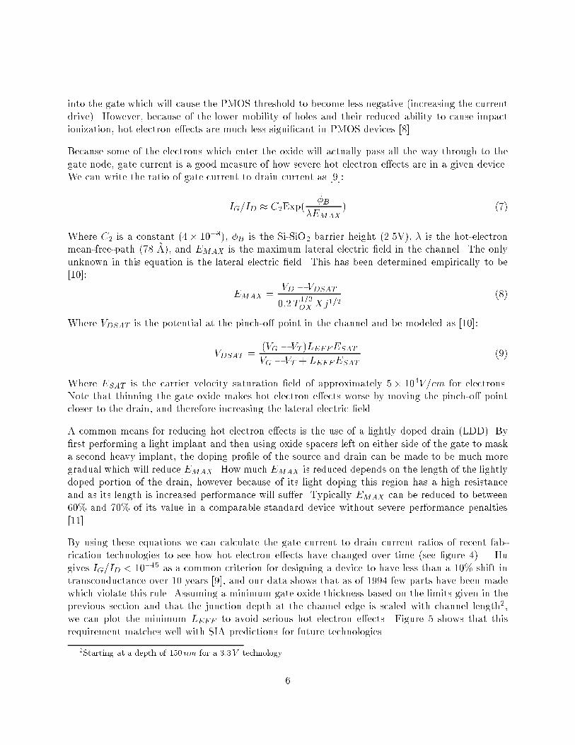
into the gate which will cause the PMOS threshold to become less negative (increasing the current
drive). However, because of the lower mobility of holes and their reduced ability to cause impact
ionization, hot electron e�ects are much less signi�cant in PMOS devices [8].
Because some of the electrons which enter the oxide will actually pass all the way through to the
gate node, gate current is a good measure of how severe hot electron e�ects are in a given device.
We can write the ratio of gate current to drain current as [9]:
IG=ID � C2Exp(�B
�EMAX) (7)
Where C2 is a constant (4� 10�3), �B is the Si-SiO2 barrier height (2.5V), � is the hot-electron
mean-free-path (78 �A), and EMAX is the maximum lateral electric �eld in the channel. The only
unknown in this equation is the lateral electric �eld. This has been determined empirically to be
[10]:
EMAX =VD � VDSAT
0:2T1=3OXXj1=2
(8)
Where VDSAT is the potential at the pinch-o� point in the channel and be modeled as [10]:
VDSAT =(VG � VT )LEFFESAT
VG � VT + LEFFESAT(9)
Where ESAT is the carrier velocity saturation �eld of approximately 5� 104V=cm for electrons.
Note that thinning the gate oxide makes hot electron e�ects worse by moving the pinch-o� point
closer to the drain, and therefore increasing the lateral electric �eld.
A common means for reducing hot electron e�ects is the use of a lightly doped drain (LDD). By
�rst performing a light implant and then using oxide spacers left on either side of the gate to mask
a second heavy implant, the doping pro�le of the source and drain can be made to be much more
gradual which will reduce EMAX . How much EMAX is reduced depends on the length of the lightly
doped portion of the drain, however because of its light doping this region has a high resistance
and as its length is increased performance will su�er. Typically EMAX can be reduced to between
60% and 70% of its value in a comparable standard device without severe performance penalties
[11].
By using these equations we can calculate the gate current to drain current ratios of recent fab-
rication technologies to see how hot electron e�ects have changed over time (see �gure 4). Hu
gives IG=ID < 10�15 as a common criterion for designing a device to have less than a 10% shift in
transconductance over 10 years [9], and our data shows that as of 1994 few parts have been made
which violate this rule. Assuming a minimum gate oxide thickness based on the limits given in the
previous section and that the junction depth at the channel edge is scaled with channel length2,
we can plot the minimum LEFF to avoid serious hot electron e�ects. Figure 5 shows that this
requirement matches well with SIA predictions for future technologies.
2Starting at a depth of 150 nm for a 3:3V technology
6

� Vdd = 5.0V Vdd = 3.3V� Vdd = 2.5V
|80
|82
|84
|86
|88
|90
|92
|94
|20
|40
|60
|80
|100
|120
|140
|160
|180
Year
EM
AX (
kV/c
m)
Ig/Id = 10-15
Ig/Id = 10-13
�
�
�
�
���
�
�
��
�
�
�
�
�
�
�
�
�
�
���
���
�
��
�
�
���
�
��
Figure 4: Channel Fields vs Year
� SIA Roadmap
|1.0
|1.5
|2.0
|2.5
|3.0
|3.5
|0.00
|0.05
|0.10
|0.15
|0.20
|0.25
|0.30
Vdd (V)
Hot Electron Min LEFF
LE
FF (
um)
�
�
�
�
Figure 5: Minimum LEFF
7

2.4 Short Channel E�ects
As MOSFET channel length is reduced, the device threshold becomes dependent on L and VDS.
These deviations from the ideal threshold model are known as the short channel e�ect and drain
induced barrier lowering (DIBL) respectively [12]. For sub-micron devices decreasing L and in-
creasing VDS will drive the threshold down as more of the channel region becomes depleted by
the source and drain regions instead of the gate. At very high VDS the depletion regions of the
source and drain can touch causing large amounts of current to ow uncontrolled by the gate. This
phenomenon is known as punch-through. All these e�ects can be reduced by increasing the channel
doping to reduce the size of the source and drain depletion regions and by decreasing the gate oxide
thickness to give the gate more control over the channel region. Since all these problems are related
and solved in the same manner, this paper considers only the limitation of DIBL. The SPICE Level
3 model for DIBL is based on the work of Masuda and is as follows [2]:
�VT =�K �ETACOX � L3
EFF
VDS (10)
Where K = 8:14� 10�22 and ETA is a curve �tting parameter. However, Masuda's model was
based on devices with channel lengths all over 1�m. To better predict DIBL in sub-micron devices
we need to use a more recent model. A model presented in 1993 by Liu and intended for use with
devices between 0:1�m and 1�m is as follows [13]:
�VT = (e�LEFF =l + e�LEFF =2l(1 + VDSPB+PHI
)�1=2)VDS (11)
l = 0:1(XJ TOXX2DEP )
1=3 (12)
XDEP =p(2�Si PHI)=(qNSUB) (13)
Where XDEP is the vertical depletion width in the channel. In order to be able to use SPICE to
simulate scaled devices, we must model how curve �tting parameters such as ETA will vary as we
scale other device parameters. By comparing the SPICE DIBL model with Liu's model we �nd
that to make the two models give similar results we should scale ETA as follows:
ETA / S0:5OXS
0:25V DD
SSUBS1:5L
(14)
Where SOX , SVDD, SSUB, and SL are the scaling factors for gate oxide thickness, power supply
voltage, channel doping, and channel length respectively. Figure 6 shows the �t between Liu's
model and the SPICE model when scaling length alone and setting ETA accordingly. By using
Liu's model with the minimum values of TOX and LEFF which meet the requirements for oxide
breakdown and hot electron e�ects already discussed, we can calculate the minimum channel doping
for a given variance in threshold. A reasonable requirement for the maximum threshold variance
due to DIBL is [2]:
�VT < 0:25VT (15)
Assuming this requirement the minimum channel doping for a given supply voltage is shown in
�gure 7.
8
SPICE Model
|0.1
|0.2
|0.5
|0.7
|0.9
|1.1
|0.0
|0.9
|1.8
|2.7
|3.6
|4.5
|5.4
|6.3
|7.2
|8.1
dV
t (V
)
Ldrawn (um)
Figure 6: Drain Induced Barrier Lowering
|1.0
|1.5
|2.0
|2.5
|3.0
|3.5
|5.0e+16
|1.0e+17
|1.5e+17
|2.0e+17
|2.5e+17
|3.0e+17
Vdd (V)
Nsu
b (c
m^-
3)
∆Vt < 0.25Vt
Figure 7: Minimum Channel Doping
9
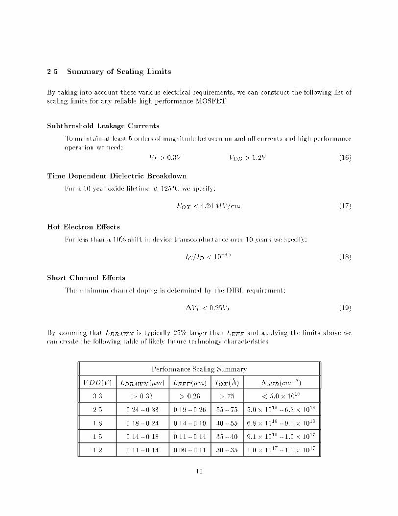
2.5 Summary of Scaling Limits
By taking into account these various electrical requirements, we can construct the following list of
scaling limits for any reliable high performance MOSFET.
Subthreshold Leakage Currents
To maintain at least 5 orders of magnitude between on and o� currents and high performance
operation we need:
VT > 0:3V VDD > 1:2V (16)
Time Dependent Dielectric Breakdown
For a 10 year oxide lifetime at 125�C we specify:
EOX < 4:24MV=cm (17)
Hot Electron E�ects
For less than a 10% shift in device transconductance over 10 years we specify:
IG=ID < 10�15 (18)
Short Channel E�ects
The minimum channel doping is determined by the DIBL requirement:
�VT < 0:25VT (19)
By assuming that LDRAWN is typically 25% larger than LEFF and applying the limits above we
can create the following table of likely future technology characteristics.
Performance Scaling Summary
V DD(V ) LDRAWN (�m) LEFF (�m) TOX(�A) NSUB(cm�3)
3.3 > 0.33 > 0.26 > 75 < 5:0� 1016
2.5 0.24 - 0.33 0.19 - 0.26 55 - 75 5:0� 1016 - 6:8� 1016
1.8 0.18 - 0.24 0.14 - 0.19 40 - 55 6:8� 1016 - 9:1� 1016
1.5 0.14 - 0.18 0.11 - 0.14 35 - 40 9:1� 1016 - 1:0� 1017
1.2 0.11 - 0.14 0.09 - 0.11 30 - 35 1:0� 1017 - 1:1� 1017
10

Performance scaling predicts a minimum drawn channel length of 0:11�m for standard LDD devices,
but this is not intended to represent the ultimate end of advancement in MOSFET technology.
These constraints are merely trying to predict the limits of scaling current technologies without any
radical changes in the construction or operation of the devices. New semiconductor materials, oxide
materials, or device structures will likely carry us beyond the limits standard MOSFET technologies.
However, the cost and uncertainty associated with incorporating large changes in device design or
manufacturing make it unlikely these new fabrication techniques will be implemented until we have
scaled very close to the limits of current technologies.
2.6 Performance Scaling of SPICE Level 3 Model
Using these scaling requirements for each of our fabrication parameters and writing all other model
parameters as functions of these scaling factors, we can create a scalable SPICE model that will
simulate devices meeting all of our electrical constraints for drawn lengths down to 0:11�m. The
scaling factors for the various parameters are as follows:
Scaling SPICE Level 3 Model
Description Parameter Generalized Performance
Scaling Scaling
Device Dimensions L, W 1=SL 1=S
Oxide Thickness TOX 1=SOX 1=S0:92
Channel Doping NSUB SSUB S1:28
Power Supply VDD 1=SVDD 1=S0:92
Junction Depth XJ 1=SL 1=S
Half Di� Width HDIF 1=SL 1=S
Junction Cap CJpSSUB S0:64
Sidewall Cap CJSWpSSUB=SL 1=S0:36
Gate Sidewall Cap CJGATEpSSUB=SL 1=S0:36
DIBL ETA S0:5OXS
0:25VDD=(S
1:5L SSUB) 1=S2:09
Channel Modulation KAPPA 1 1
Narrow Width Factor DELTA 1 1
Di�usion Sheet Res RSH SL S
Note how close these scaling factors are to Denard's constant �eld scaling. This is because after
years of not scaling power supply voltages with device dimensions, we have now reached the point
11

where gate oxide and channel �elds are at their maximum tolerable levels. In order to continue to
scale device dimensions and maintain reliability, we are now forced to do something very close to
constant �eld scaling.
3 Delay of Scaled Devices
Using our scaled SPICE models we can simulate device performance over a wide range of drawn
lengths.
|0.15
|0.25
|0.35
|0.45
|0.55
|0.65
|0.75
|0.85
|20
|40
|60
|80
|100
|120
|140
Feature Size (um)
Del
ay (
ps)
Figure 8: Fanout of 4 Inverter Delay
Figure 8 shows the delay of an inverter driving a fanout of 4 over a range of drawn lengths. The
improvement in performance is basically linear as we would expect from heavily velocity saturated
devices where delay is as follows:
t / Fanout � LVMAX
(20)
4 Scaling of Interconnects
In addition to the scaling of the devices, it is also important to examine the scaling of the de-
vice interconnects and how their changing resistance and capacitance will e�ect wire delay. The
resistance of the line per unit length can be written as
RL = �=(WINTTINT) (21)
12

Where � is the resistivity of the interconnect material, WINT is the interconnect's width, and TINTis its thickness.
To properly model the capacitance per unit length, we must take into account area and fringe
capacitance to the substrate as well as coupling capacitance to adjacent wires. A good empirical
model of capacitance is as follows [15]:
CSUB=�ox = 1:15WINT
TFOX+ 2:8(
TINT
TFOX)0:222 (22)
(23)
CCOUP=�ox = (0:03WINT
TFOX+ 0:83
TINT
TFOX� 0:07(
TINT
TFOX)0:222)(
WSP
TFOX)�1:34 (24)
(25)
CTOTAL = CSUB + 2CCOUP (26)
Where TFOX is the thickness of the �eld oxide, andWSP is the width of the space between adjacent
lines. Given these models for resistance and capacitance we can compare the three basic intercon-
nect scaling schemes suggested by Bakoglu, ideal scaling, quasi-ideal scaling, and constant-R scaling
[14].
Scaling Local Interconnects
Description Parameter Ideal Quasi-Ideal Constant-R SIAScaling Scaling Scaling Scaling
Width WINT 1=S 1=S 1=pS 1=S
Spacing WSP 1=S 1=S 1=pS 1=S
Thickness TINT 1=S 1=pS 1=
pS 1=S0:41
Field Oxide TFOX 1=S 1=pS 1=
pS 1=S0:43
Aspect Ratio Ar 1pS 1 S0:61
Res per Length RL S2 S1:5 S S1:60
Cap per Length CL 1 0:9 + 0:1S 1 S0:31
RC per Length RLCL S2 0:9S1:5+ 0:1S2:5 S S1:91
Figure 9 shows that constant-R scaling is clearly superior in minimizing delay, however this scheme
means that the wire widths and spacing will not scale as quickly as the device sizes3. Very quickly
circuit area will become wire limited and integration will su�er. Ideal scaling has the advantages of
scaling wire pitch with device size and keeping a constant aspect ratio, but it has the worst delay
3This �gure assumes that for a scaling factor of 1, WINT = WSP = TINT = TFOX = 1�m
13

� Ideal Scaling Quasi-Ideal Scaling� Constant R Scaling
|1
|2
|3
|4
|5
|6
|7
|8
|9
|10
|0
|70
|140
|210
|280
|350
|420
|490
|560
|630
Scale
ps/
mm
2
�
�
�
�
�
�
�
�
�
�
� � � � � � � � � �
Figure 9: Wire Delay
of the three schemes. Therefore, in order to avoid becoming severely wire limited while keeping
delay to a minimum, quasi-ideal scaling is a good middle ground. The major disadvantage is the
increase in aspect ratio which can cause step coverage problems, but the inclusion of via-hole �lling
and dielectric planarization steps in modern processes has allowed increasing aspect ratios to be
tolerated. The table above shows that the interconnect scaling predicted by the SIA roadmap
matches very closely with quasi-ideal scaling.
5 Conclusions
This paper has shown that as MOSFET channel lengths are scaled, the ranges of oxide thickness,
channel doping, and power supply voltage which will produce a reliable device are all reduced. For
MOSFETs with dimensions of greater than 1�m di�erent manufacturers could produce working
devices with very di�erent oxide thicknesses and channel dopings. However, as device dimensions
move below 0:5�m toward 0:1�m all manufacturers will be forced to converge on the very narrow
range of parameters which will produce a working device.
In the past constant �eld scaling has been an excellent predictor of trends for gate oxide thickness
and channel doping but not for supply voltages. However, recently �elds in the gate oxide and the
channel have become high enough to force scaling of the supply voltage. Therefore, future scaling
trends should closely follow constant �eld scaling.
If the proper means of economical fabrication can be developed bulk CMOS MOSFETs can be scaled
14

down to drawn lengths of approximately 0:10�m. The route cause of this limit is the inability to
scale the slope of the subthreshold current.
There are at least three basic approaches for scaling devices below 0:10�m. The subthreshold slope
could be improved by cooling devices signi�cantly below room temperature or by using Silicon-On-
Insulator (SOI) devices. Alternatively, new gate oxide materials with higher permittivities, higher
breakdown �elds, and which are more resistant to hot electron e�ects could reduce the need for
further supply voltage reductions. However, even though such devices are electrically feasible it
may not be possible to economically mass produce them.
15

Appendix A { SIA Roadmap
1994 SIA Roadmap Summary
1st DRAM Year 1995 1998 2001 2004 2007
Feature Size (�m) 0.35 0.25 0.18 0.13 0.10
LEFF (�m) 0.28 0.20 0.14 0.10 < 0:10
TOX(�A) 83 73 50 45 34
Vdd (V ) 3.3 2.5 1.8 1.5 1.2
XJ (nm) 70-150 50-120 30-80 20-60 15-45
WINT (�m) 0.40 0.30 0.22 0.15 0.11
WSP (�m) 0.60 0.45 0.33 0.25 0.16
TINT (�m) 0.60 0.60 0.55 0.45 0.39
Wire Aspect Ratio 1.5 2 2.5 3 3.5
Wire Res (=�m) 0.15 0.19 0.29 0.82 1.34
Wire Cap (fF=�m) 0.17 0.19 0.21 0.24 0.27
16

Appendix B { Scalable HSPICE Device Models
* To use model simply set Length parameter to desired drawn device length
.param BaseLength = 0.8u
.param s = 'BaseLength/Length'
* The parameters which can be set the fabrication process are
* Length, Tox, Nsub, and Vdd
.param Slen = s
.param Stox = 'pwr(s, 0.92)'
.param Svdd = 'pwr(s, 0.92)'
.param Ssub = 'pwr(s, 1.28)'
.param vSupply = '7 / Svdd'
.param Seta = 'sqrt(Stox)*pwr(Svdd, 0.25)/(pwr(Slen, 1.5)*Ssub)'
.MODEL TN NMOS LEVEL=3
*
+ * Parameters which can be scaled directly
+ TOX = '135e-10 / Stox' * Gate oxide thickness
+ NSUB = '5e16 * Ssub' * Channel doping
*
+ * Parameters which are functions of scaled parameters
+ XJ = '0.16u / Slen' * Junct depth/Short channel effects
+ HDIF = '1u / Slen' * Dis from gate to drain center
+ CJ = '9e-5 * sqrt(Ssub)' * Bottom junction capacitance
+ CJSW = '5e-10 * sqrt(Ssub)/Slen' * Sidewall junction capacitance
+ CJGATE = '3e-10 * sqrt(Ssub)/Slen' * Gate-edge sidewall capacitance
+ ETA = '0.03 * Seta' * DIBL
+ RSH = '40 * Slen' * Diff Sheet Resistance
*
+ * Parameters which are independent of scaling
+ TPG = 1 * Gate poly same type as source and drain
+ ACM = 3 * Source/drain Diffusion area model
+ KAPPA = 0.2 * Channel Length Modulation
+ THETA = 0.12 * Surface Mobility Reduction
+ DELTA = 0.1 * Narrow Width Effects
+ DELVTO = 0.419 * Zero bias threshold offset
+ U0 = 580 * Carrier mobility
+ VMAX = 2e5 * Velocity Saturation
17

.MODEL TP PMOS LEVEL=3
*
+ * Parameters which can be scaled directly
+ TOX = '135e-10 / Stox' * Gate oxide thickness
+ NSUB = '5e16 * Ssub' * Channel doping
*
+ * Parameters which are functions of scaled parameters
+ XJ = '0.16u / Slen' * Junct depth/Short channel effects
+ HDIF = '1u / Slen' * Dis from gate to drain center
+ CJ = '9e-5 * sqrt(Ssub)' * Bottom junction capacitance
+ CJSW = '5e-10 * sqrt(Ssub)/Slen' * Sidewall junction capacitance
+ CJGATE = '3e-10 * sqrt(Ssub)/Slen' * Gate-edge sidewall capacitance
+ ETA = '0.03 * Seta' * DIBL
+ RSH = '110 * Slen' * Diff Sheet Resistance
*
+ * Parameters which are independent of scaling
+ TPG = 1 * Gate poly same type as source and drain
+ ACM = 3 * Source/drain Diffusion area model
+ KAPPA = 0.2 * Channel Length Modulation
+ THETA = 0.12 * Surface Mobility Reduction
+ DELTA = 0.1 * Narrow Width Effects
+ DELVTO = -0.419 * Zero bias threshold offset
+ U0 = 175 * Carrier mobility
+ VMAX = 2e5 * Velocity Saturation
Appendix C { Scalable HSPICE Wire Models
* To use model simply set Length parameter to desired drawn device length
.param BaseLength = 0.8u
.param s = 'BaseLength/Length'
* The parameters which can be set in the metalization process are
* field oxide thickness, and wire thickness, wire width, and
* wire spacing
* Bakoglu's quasi-ideal scaling
.param Swid = s
.param Sfox = 'sqrt(s)'
.param Sthk = 'sqrt(s)'
18
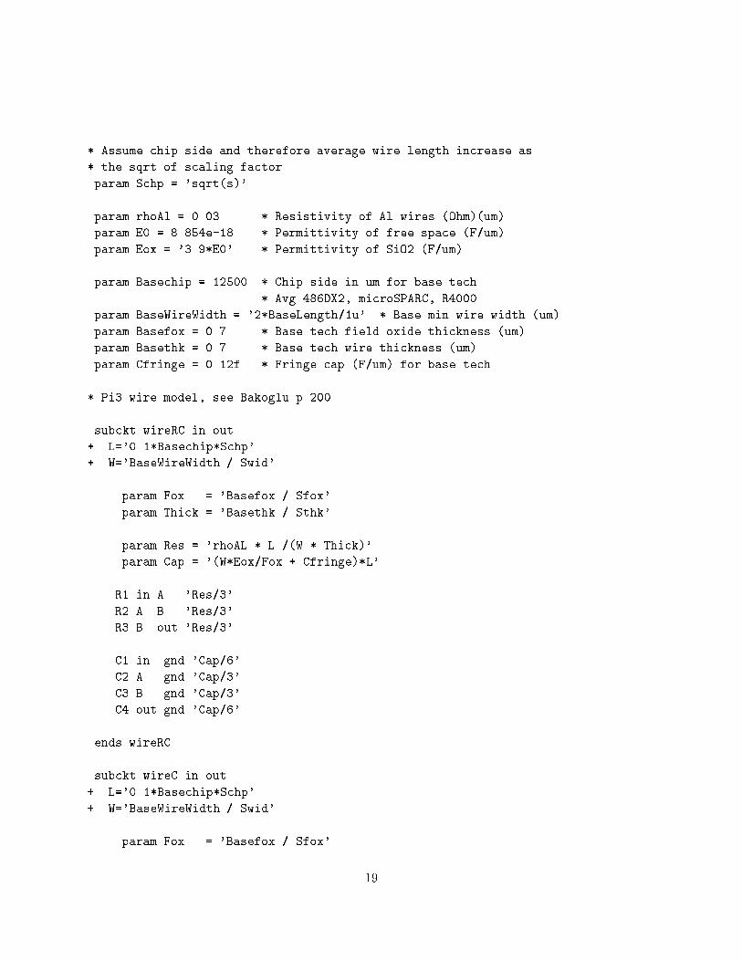
* Assume chip side and therefore average wire length increase as
* the sqrt of scaling factor
.param Schp = 'sqrt(s)'
.param rhoAl = 0.03 * Resistivity of Al wires (Ohm)(um)
.param E0 = 8.854e-18 * Permittivity of free space (F/um)
.param Eox = '3.9*E0' * Permittivity of SiO2 (F/um)
.param Basechip = 12500 * Chip side in um for base tech
* Avg 486DX2, microSPARC, R4000
.param BaseWireWidth = '2*BaseLength/1u' * Base min wire width (um)
.param Basefox = 0.7 * Base tech field oxide thickness (um)
.param Basethk = 0.7 * Base tech wire thickness (um)
.param Cfringe = 0.12f * Fringe cap (F/um) for base tech
* Pi3 wire model, see Bakoglu p.200
.subckt wireRC in out
+ L='0.1*Basechip*Schp'
+ W='BaseWireWidth / Swid'
.param Fox = 'Basefox / Sfox'
.param Thick = 'Basethk / Sthk'
.param Res = 'rhoAL * L /(W * Thick)'
.param Cap = '(W*Eox/Fox + Cfringe)*L'
R1 in A 'Res/3'
R2 A B 'Res/3'
R3 B out 'Res/3'
C1 in gnd 'Cap/6'
C2 A gnd 'Cap/3'
C3 B gnd 'Cap/3'
C4 out gnd 'Cap/6'
.ends wireRC
.subckt wireC in out
+ L='0.1*Basechip*Schp'
+ W='BaseWireWidth / Swid'
.param Fox = 'Basefox / Sfox'
19

.param Cap = '(W*Eox/Fox + Cfringe)*L'
R1 in out 0.001
C1 out gnd 'Cap'
.ends wireC
Appendix D { Mathematica Models
TOXBREAK
<< rules.m
(* For a given power supply return the minimum safe gate oxide *)
(* thickness to avoid oxide breakdown in time tbd. *)
ToxBreak[vdd_, tbd_:(20*10*year)] := 1.5(1.1vdd/Ebreak[tbd]);
(* Return the maximum electric field for a given oxide thickness *)
(* and desired time to breakdown. *)
(* Lifetime is measured at 25C, to calculate breakdown field for *)
(* 125C, multiply TBD by 20. *)
Ebreak[tbd_:(10*year)] :=
Block [ { t0 = 10^-11*sec,
G = 350*10^6*(V/cm) },
Return[ N[ G/Log[tbd/t0] ] ]
]
(* K. Schuegraf and C. Hu, "Hole Injection SiO2 Breakdown Model *)
(* for Very Low Voltage Lifetime Extrapolation", IEEE Tran. on *)
(* Electron Devices, May 1994, p.761. *)
(* K. Schuegraf and C. Hu, "Effects of Temperature and Defects *)
(* on Breakdown Lifetime of Thin SiO2 at Very Low Voltages", *)
(* IEEE Tran. on Electron Devices, July 1994, p.1227. *)
20

LEFF
<< rules.m
<< toxbreak.m
(* Return the minimum Leff which will not suffer severe hot *)
(* electron effects at a given supply voltage assuming the *)
(* minimum gate oxide thickness for that voltage and that *)
(* a lightly doped drain structure is being used. *)
(* Hu, C., "Hot-Electron Induced MOSFET Degradation -- Model, *)
(* Monitor, and Improvement", IEEE Tran on Electron Devices, *)
(* 1985, p. 375. *)
(* FRF is from Mayaram, "A Model for the Electric Field in *)
(* Lightly Doped Drain Structures", ITED, 1987, p. 1509 *)
Leff[vdd_] :=
Block [ { FRF = 0.7 (* Field Reduction Factor for LDD *) },
Ldep = 0.2*(m^(1/6)) ToxBreak[vdd]^(1/3) Xj[vdd]^(1/2);
vdsat = vdd - Ecrit[]*Ldep/FRF;
Return[ Lsat[vdsat, vdd] ];
];
(* Return value for source/drain junction depth at channel *)
(* for a given value of vdd. These values reflect the *)
(* worst case (deepest junctions) from the SIA roadmap. *)
Xj[vdd_] := 150*10^-9*m / (3.3V/vdd)^(1/0.8)
(* Return the lateral electric field in the channel needed to *)
(* produce the given ratio of gate current to drain current. *)
(* A ratio of 10^-15 is sometimes given as the maximum *)
(* acceptable ratio. *)
(* Hu, C., "Hot-electron Effects in MOSFET's", IEDM, 1983, p. 176 *)
Ecrit[ iratio_:(10^-15)] :=
Block [ { C2 = 4*10^-3,
PhiB = 2.5*(V),
21
lambda = 78*10^-10*(m) },
Return[ N[ -PhiB/(lambda Log[iratio/C2]) ] ];
];
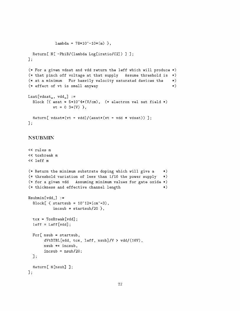
(* For a given vdsat and vdd return the leff which will produce *)
(* that pinch off voltage at that supply. Assume threshold is *)
(* at a minimum. For heavily velocity saturated devices the *)
(* effect of vt is small anyway. *)
Lsat[vdsat_, vdd_] :=
Block [{ esat = 5*10^4*(V/cm), (* electron vel sat field *)
vt = 0.3*(V) },
Return[ vdsat*(vt - vdd)/(esat*(vt - vdd + vdsat)) ];
];
NSUBMIN
<< rules.m
<< toxbreak.m
<< leff.m
(* Return the minimum substrate doping which will give a *)
(* threshold variation of less than 1/16 the power supply *)
(* for a given vdd. Assuming minimum values for gate oxide *)
(* thickness and effective channel length. *)
Nsubmin[vdd_] :=
Block[ { startsub = 10^12*(cm^-3),
incsub = startsub/20 },
tox = ToxBreak[vdd];
leff = Leff[vdd];
For[ nsub = startsub,
dVtDIBL[vdd, tox, leff, nsub]/V > vdd/(16V),
nsub += incsub,
incsub = nsub/20;
];
Return[ N[nsub] ];
];
22

(* This DIBL model is based on Liu, Z., "Threshold Voltage Model *)
(* for Deep-Submicrometer MOSFET's", IEEE Tran. on Elec. Devices, *)
(* Jan '93, p.86. *)
dVtDIBL[vds_, tox_, leff_, nsub_] :=
Block[ { pb = 0.8V,
l = Lchar[tox, Xj[vds], nsub] },
dVds = Exp[-leff/l] + Exp[-leff/(2l)]/Sqrt[1 + vds/(pb + phi[nsub])];
Return[ vds*dVds];
];
Lchar[Tox_, XJ_, nsub_] :=
Block[ { tox = Tox/(10^-10*m),
xj = XJ/(10^-6*m),
wch = Wch[nsub]/(10^-6*m) },
Return[ 0.1(tox * xj * wch^2)^(1/3) * (10^-6*m) ];
];
Wch[nsub_, vsb_:(0)] := Sqrt[2Esi(phi[nsub] + vsb*V)/(q nsub)];
phi[nsub_] = 2*0.026V*Log[nsub/ni];
WIREDELAY
<< rules.m
(* T. Sakurai, "Simple Formulas for Two and Three Dimensional
Capacitances", IEEE Tran. on Electron Devices, 1983, p. 183. *)
(* All lengths are in microns *)
(* w = wire width *)
(* t = wire thickness *)
(* h = oxide thickness *)
(* sp = wire spacing *)
GroundCap[w_:(1), t_:(1), h_:(1)] :=
Eox*(1.15(w/h) + 2.8(t/h)^0.222)
CoupleCap[w_:(1), t_:(1), h_:(1), sp_:(1)] :=
23

2Eox*(0.03(w/h) + 0.83(t/h) - 0.07(t/h)^0.222)(sp/h)^-1.34
WireCap[w_:(1), t_:(1), h_:(1), sp_:(1)] :=
GroundCap[w, t, h] + CoupleCap[w, t, h, sp]
WireRes[w_:(1), t_:(1)] := rhoAl/(w*t*um^2)
WireDelay[w_:(1), t_:(1), h_:(1), sp_:(1)] :=
WireRes[w, t] * WireCap[w, t, h, sp]
RULES
(* This file provides rules for changing units and simplifying *)
(* expressions. As well as some useful physical constants. *)
(* Factor square roots *)
Unprotect[Sqrt]
Sqrt[x_*y_] := Sqrt[x]*Sqrt[y]
Sqrt[x_/y_] := Sqrt[x]/Sqrt[y]
Sqrt[x_^n_] := x^(n/2)
Protect[Sqrt]
(* Factor Powers *)
Unprotect[Power]
Power[x_*y_, n_] := Power[x,n]*Power[y,n]
Power[x_/y_, n_] := Power[x,n]/Power[y,n]
Power[x_^m_, n_] := Power[x,m*n]
Protect[Power]
(* Change centimeters to meters *)
cm := 0.01m
(* Change microns to meters *)
um := 10^-6*m
(* Change angstroms to meters *)
AA := 10^-10*m
(* Change Farads into Coloumbs per Volt *)
F := C/V
(* Change Ohms *)
24
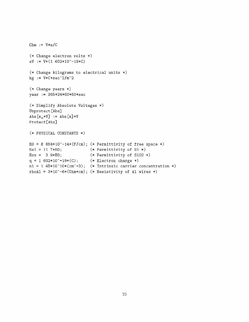
Ohm := V*s/C
(* Change electron volts *)
eV := V*(1.602*10^-19*C)
(* Change kilograms to electrical units *)
kg := V*C*sec^2/m^2
(* Change years *)
year := 365*24*60*60*sec
(* Simplify Absolute Voltages *)
Unprotect[Abs]
Abs[x_*V] := Abs[x]*V
Protect[Abs]
(* PHYSICAL CONSTANTS *)
E0 = 8.854*10^-14*(F/cm); (* Permittivity of free space *)
Esi = 11.7*E0; (* Permittivity of Si *)
Eox = 3.9*E0; (* Permittivity of SiO2 *)
q = 1.602*10^-19*(C); (* Electron charge *)
ni = 1.45*10^10*(cm^-3); (* Intrinsic carrier concentration *)
rhoAl = 3*10^-6*(Ohm*cm); (* Resistivity of Al wires *)
25
References
[1] R. Denard. "Design of Ion-Implanted MOSFETs with Very Small Dimensions", IEEE Journal
of Solid State Circuits, 1974, p. 256.
[2] H. Masuda. "Characteristics and Limitation of Scaled-Down MOSFETs Due to Two-
Dimensional Field E�ect", IEEE Transactions on Electron Devices, 1979, p. 980.
[3] J. P�ester. "Performance Limits of CMOS ULSI," IEEE Transactions on Electron Devices,
1985, pp. 333.
[4] K. Yamabe. "Time-Dependent Dielectric Breakdown of Thin Thermally Grown SiO2 Films",
IEEE Transactions on Electron Devices, 1985, p. 423.
[5] R. Moazzami. "Projecting the Minimum Acceptable Oxide Thickness For Time-Dependent
Dielectric Breakdown", International Electronic Devices Meeting, 1988, p. 710.
[6] K. Schuegraf. "E�ects of Temperature and Defects on Breakdown Lifetime of Thin SiO2 at
Very Low Voltages", IEEE Transactions on Electron Devices, 1994, p. 1227.
[7] "The National Technology Roadmap for Semiconductors", Semiconductor Industry Associa-
tion, 1994.
[8] T. Hayashi. "Hot Carrier Injection in PMOSFETs", OKI Technical Review, Sept. 1991, p. 59.
[9] C. Hu. "Hot-Electron E�ects in MOSFETs", International Electronic Devices Meeting, 1983,
p. 176.
[10] C. Hu. "Hot-Electron Induced MOSFET Degradation { Model, Monitor, and Improvement",
IEEE Transactions on Electron Devices, 1985, p. 375.
[11] Mayaram. "A Model for the Electric Field in Lightly Doped Drain Structures", IEEE Trans-
actions on Electron Devices, 1987, p.1509.
[12] R. Troutman. "VLSI Limitations from Drain-Induced Barrier Lowering", IEEE Transactions
on Electron Devices, 1979, p. 461.
[13] Z. Liu. "Threshold Voltage Model for Deep-Sub-micrometer MOSFETs", IEEE Transactions
on Electron Devices, 1993, p. 86.
[14] H. Bakoglu. Circuits, Interconnections, and Packaging for VLSI, Addison-Wesley, 1990.
[15] T. Sakurai. "Simple Formulas for Two and Three Dimensional Capacitances", IEEE Transac-
tions on Electron Devices, 1983, p. 183.
26


