Graphene-based flexible and stretchable thin film transistors Chao Yan, a Jeong Ho Cho * b and Jong-Hyun Ahn * a Received 25th April 2012, Accepted 24th May 2012 DOI: 10.1039/c2nr30994g Graphene has been attracting wide attention owing to its superb electronic, thermal and mechanical properties. These properties allow great applications in the next generation of optoelectronics, where flexibility and stretchability are essential. In this context, the recent development of graphene growth/ transfer and its applications in field-effect transistors are involved. In particular, we provide a detailed review on the state-of-the-art of graphene-based flexible and stretchable thin film transistors. We address the principles of fabricating high-speed graphene analog transistors and the key issues of producing an array of graphene-based transistors on flexible and stretchable substrates. It provides a platform for future work to focus on understanding and realizing high-performance graphene-based transistors. 1. Introduction The outstanding physical and chemical properties of graphene, a single atomic layer of carbon atoms, have attracted significant attention. One of the most important advantages of graphene in the field of electronics is its superb charge carrier mobility. The mobility of ideal exfoliated graphene spans an extraordinarily large range, from 10 000–15 000 cm 2 V 1 s 1 on SiO 2 insulating substrates to 200 000 cm 2 V 1 s 1 in suspended structures, 1–5 suggesting that graphene may potentially outperform established inorganic materials in certain applications, such as high- frequency transistors. Although useful devices have been prepared based on exfoliated graphene, 6 the tiny size of exfoli- ated graphene films limits the practical utility of such graphene in electronic applications. Recent studies designed to address this issue have explored the preparation of large-area high-quality graphene via epitaxial growth 7,8 or chemical vapor deposition (CVD). 9,10 Many research groups have reported the fabrication of graphene-based transistors via the epitaxial growth of Chao Yan Chao Yan is currently a research professor with Prof. Jong-Hyun Ahn at Sungkyunkwan Univer- sity (SKKU) working on gra- phene synthesis and applications in flexible electronics. He obtained his PhD degree in polymer physics and chemistry from the Institute of Chemistry, Chinese Academy of Science (CAS) in 2007. He was a post- doctor in Kwansei-Gakuin University (Japan) and the University of Melbourne (Aus- tralia) before he joined Prof. Ahn’s group. His research interests include 2D material (e.g. graphene and hBN) synthesis and application in field-effect transistors and organic photovoltaics. Jeong Ho Cho Jeong Ho Cho is an assistant professor of SKKU Advanced Institute of Nanotechnology (SAINT) and Department of Chemical Engineering at Sung- kyunkwan University in Korea. He received his PhD (2006) from POSTECH in Chemical Engineering. He was a post- doctoral researcher in the Department of Chemical Engi- neering and Materials Science at the University of Minnesota (2006–2008) and then joined the faculty at Soongsil University from 2008. He then moved to Sungkyunkwan University from 2012. His research interests include organic field-effect transistors and sensors, and multi- functional smart surfaces. a SKKU Advanced Institute of Nanotechnology (SAINT), Center for Human Interface Nano Technology (HINT), School of Advanced Materials Science and Engineering, Sungkyunkwan University, Suwon 440-746, Republic of Korea. E-mail: [email protected]b SKKU Advanced Institute of Nanotechnology (SAINT), Center for Human Interface Nano Technology (HINT), School of Chemical Engineering, Sungkyunkwan University, Suwon 440-746, Republic of Korea. E-mail: [email protected]4870 | Nanoscale, 2012, 4, 4870–4882 This journal is ª The Royal Society of Chemistry 2012 Dynamic Article Links C < Nanoscale Cite this: Nanoscale, 2012, 4, 4870 www.rsc.org/nanoscale FEATURE ARTICLE
Transcript
Dynamic Article LinksC<Nanoscale
Cite this: Nanoscale, 2012, 4, 4870
www.rsc.org/nanoscale FEATURE ARTICLE
Graphene-based flexible and stretchab
le thin film transistors
Chao Yan,a Jeong Ho Cho*b and Jong-Hyun Ahn*a
Received 25th April 2012, Accepted 24th May 2012
DOI: 10.1039/c2nr30994g
Graphene has been attracting wide attention owing to its superb electronic, thermal and mechanical
properties. These properties allow great applications in the next generation of optoelectronics, where
flexibility and stretchability are essential. In this context, the recent development of graphene growth/
transfer and its applications in field-effect transistors are involved. In particular, we provide a detailed
review on the state-of-the-art of graphene-based flexible and stretchable thin film transistors. We
address the principles of fabricating high-speed graphene analog transistors and the key issues of
producing an array of graphene-based transistors on flexible and stretchable substrates. It provides
a platform for future work to focus on understanding and realizing high-performance graphene-based
transistors.
1. Introduction
The outstanding physical and chemical properties of graphene,
a single atomic layer of carbon atoms, have attracted significant
attention. One of the most important advantages of graphene in
the field of electronics is its superb charge carrier mobility. The
Chao Yan
Chao Yan is currently a research
professor with Prof. Jong-Hyun
Ahn at Sungkyunkwan Univer-
sity (SKKU) working on gra-
phene synthesis and applications
in flexible electronics. He
obtained his PhD degree in
polymer physics and chemistry
from the Institute of Chemistry,
Chinese Academy of Science
(CAS) in 2007. He was a post-
doctor in Kwansei-Gakuin
University (Japan) and the
University of Melbourne (Aus-
tralia) before he joined Prof.
Ahn’s group. His research
interests include 2D material (e.g. graphene and hBN) synthesis
and application in field-effect transistors and organic
photovoltaics.
aSKKU Advanced Institute of Nanotechnology (SAINT), Center forHuman Interface Nano Technology (HINT), School of AdvancedMaterials Science and Engineering, Sungkyunkwan University, Suwon440-746, Republic of Korea. E-mail: [email protected] Advanced Institute of Nanotechnology (SAINT), Center forHuman Interface Nano Technology (HINT), School of ChemicalEngineering, Sungkyunkwan University, Suwon 440-746, Republic ofKorea. E-mail: [email protected]
4870 | Nanoscale, 2012, 4, 4870–4882
mobility of ideal exfoliated graphene spans an extraordinarily
large range, from 10 000–15 000 cm2 V�1 s�1 on SiO2 insulating
substrates to 200 000 cm2 V�1 s�1 in suspended structures,1–5
suggesting that graphene may potentially outperform established
inorganic materials in certain applications, such as high-
frequency transistors. Although useful devices have been
prepared based on exfoliated graphene,6 the tiny size of exfoli-
ated graphene films limits the practical utility of such graphene in
electronic applications. Recent studies designed to address this
issue have explored the preparation of large-area high-quality
graphene via epitaxial growth7,8 or chemical vapor deposition
(CVD).9,10 Many research groups have reported the fabrication
of graphene-based transistors via the epitaxial growth of
Jeong Ho Cho
Jeong Ho Cho is an assistant
professor of SKKU Advanced
Institute of Nanotechnology
(SAINT) and Department of
Chemical Engineering at Sung-
kyunkwan University in Korea.
He received his PhD (2006)
from POSTECH in Chemical
Engineering. He was a post-
doctoral researcher in the
Department of Chemical Engi-
neering and Materials Science
at the University of Minnesota
(2006–2008) and then joined the
faculty at Soongsil University
from 2008. He then moved to
Sungkyunkwan University from 2012. His research interests
include organic field-effect transistors and sensors, and multi-
functional smart surfaces.
This journal is ª The Royal Society of Chemistry 2012
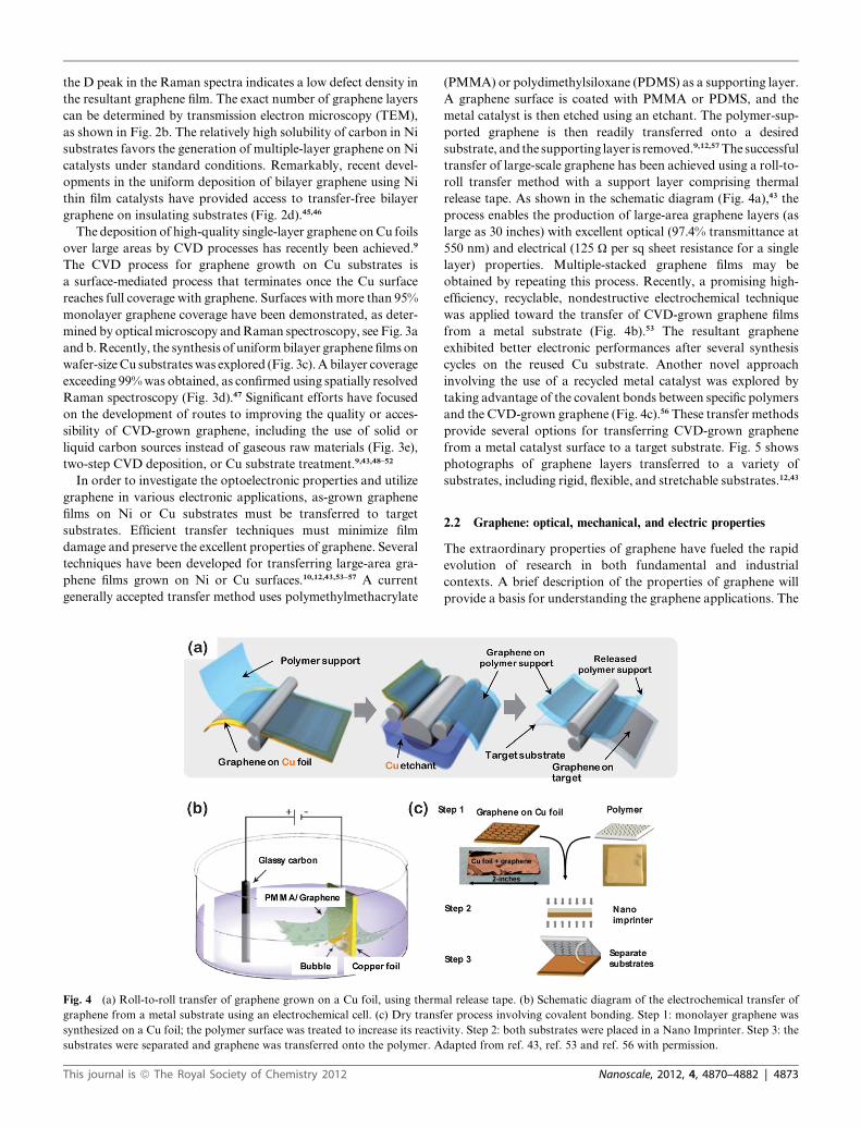
was applied toward the transfer of CVD-grown graphene films
from a metal substrate (Fig. 4b).53 The resultant graphene
exhibited better electronic performances after several synthesis
cycles on the reused Cu substrate. Another novel approach
involving the use of a recycled metal catalyst was explored by
taking advantage of the covalent bonds between specific polymers
and the CVD-grown graphene (Fig. 4c).56 These transfer methods
provide several options for transferring CVD-grown graphene
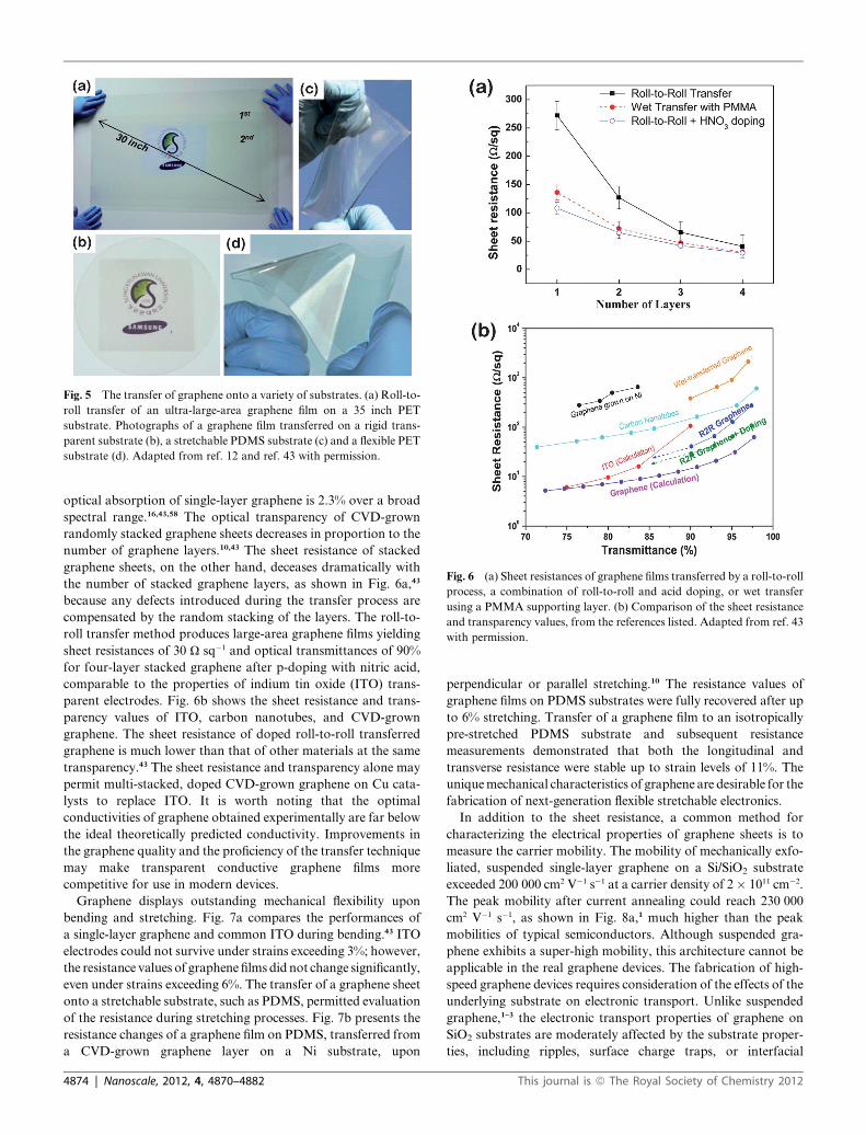
from a metal catalyst surface to a target substrate. Fig. 5 shows
photographs of graphene layers transferred to a variety of
substrates, including rigid, flexible, and stretchable substrates.12,43
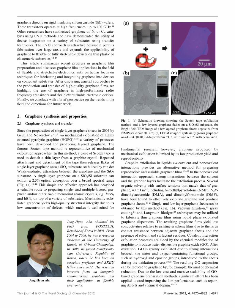
2.2 Graphene: optical, mechanical, and electric properties
The extraordinary properties of graphene have fueled the rapid
evolution of research in both fundamental and industrial
contexts. A brief description of the properties of graphene will
provide a basis for understanding the graphene applications. The
al release tape. (b) Schematic diagram of the electrochemical transfer of
er process involving covalent bonding. Step 1: monolayer graphene was
vity. Step 2: both substrates were placed in a Nano Imprinter. Step 3: the
dapted from ref. 43, ref. 53 and ref. 56 with permission.
Nanoscale, 2012, 4, 4870–4882 | 4873
Fig. 5 The transfer of graphene onto a variety of substrates. (a) Roll-to-
roll transfer of an ultra-large-area graphene film on a 35 inch PET
substrate. Photographs of a graphene film transferred on a rigid trans-
parent substrate (b), a stretchable PDMS substrate (c) and a flexible PET
substrate (d). Adapted from ref. 12 and ref. 43 with permission.
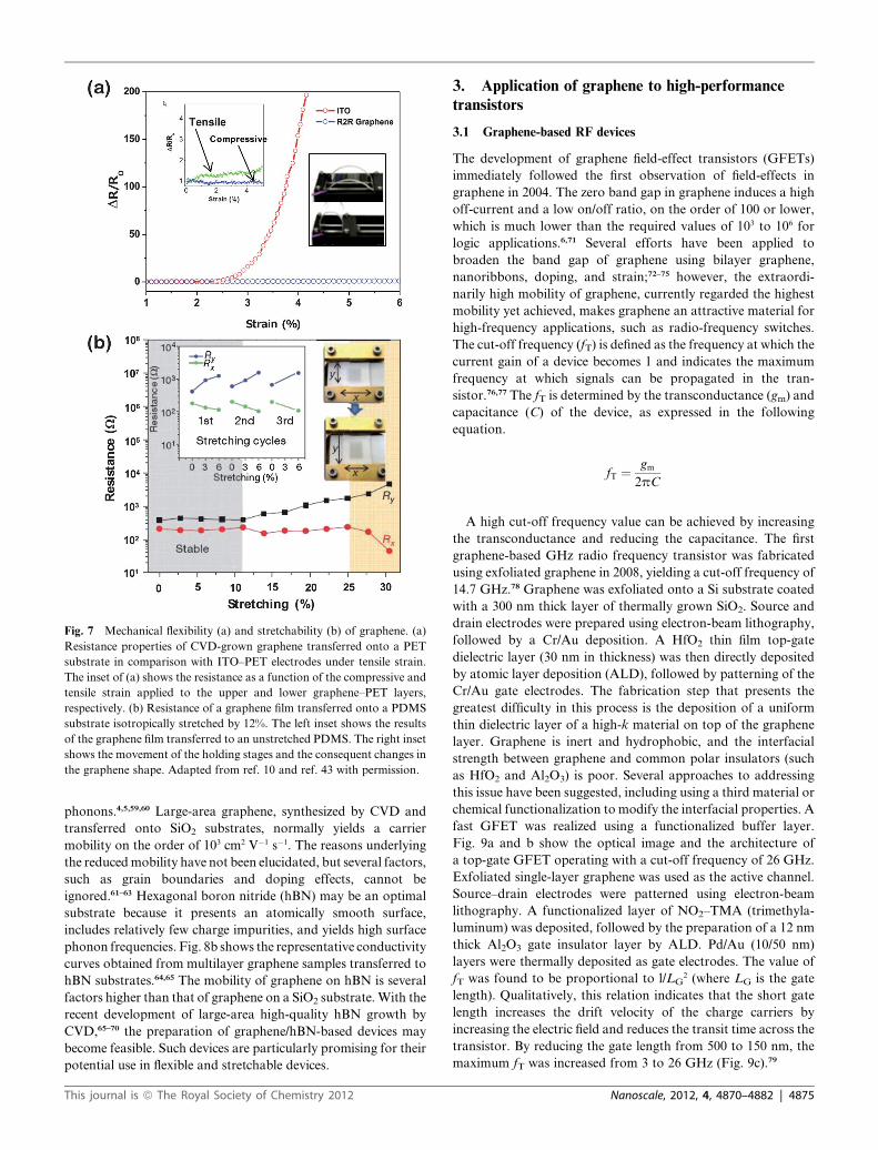
Fig. 6 (a) Sheet resistances of graphene films transferred by a roll-to-roll
process, a combination of roll-to-roll and acid doping, or wet transfer
using a PMMA supporting layer. (b) Comparison of the sheet resistance
and transparency values, from the references listed. Adapted from ref. 43
with permission.
optical absorption of single-layer graphene is 2.3% over a broad
spectral range.16,43,58 The optical transparency of CVD-grown
randomly stacked graphene sheets decreases in proportion to the
number of graphene layers.10,43 The sheet resistance of stacked
graphene sheets, on the other hand, deceases dramatically with
the number of stacked graphene layers, as shown in Fig. 6a,43
because any defects introduced during the transfer process are
compensated by the random stacking of the layers. The roll-to-
roll transfer method produces large-area graphene films yielding
sheet resistances of 30 U sq�1 and optical transmittances of 90%
for four-layer stacked graphene after p-doping with nitric acid,
comparable to the properties of indium tin oxide (ITO) trans-
parent electrodes. Fig. 6b shows the sheet resistance and trans-
parency values of ITO, carbon nanotubes, and CVD-grown
graphene. The sheet resistance of doped roll-to-roll transferred
graphene is much lower than that of other materials at the same
transparency.43 The sheet resistance and transparency alone may
permit multi-stacked, doped CVD-grown graphene on Cu cata-
lysts to replace ITO. It is worth noting that the optimal
conductivities of graphene obtained experimentally are far below
the ideal theoretically predicted conductivity. Improvements in
the graphene quality and the proficiency of the transfer technique
may make transparent conductive graphene films more
competitive for use in modern devices.
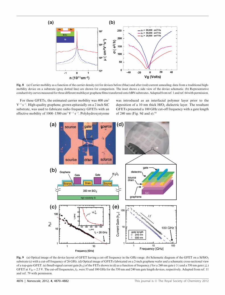
Graphene displays outstanding mechanical flexibility upon
bending and stretching. Fig. 7a compares the performances of
a single-layer graphene and common ITO during bending.43 ITO
electrodes could not survive under strains exceeding 3%; however,
the resistance values of graphene films did not change significantly,
even under strains exceeding 6%. The transfer of a graphene sheet
onto a stretchable substrate, such as PDMS, permitted evaluation
of the resistance during stretching processes. Fig. 7b presents the
resistance changes of a graphene film on PDMS, transferred from
a CVD-grown graphene layer on a Ni substrate, upon
4874 | Nanoscale, 2012, 4, 4870–4882
perpendicular or parallel stretching.10 The resistance values of
graphene films on PDMS substrates were fully recovered after up
to 6% stretching. Transfer of a graphene film to an isotropically
pre-stretched PDMS substrate and subsequent resistance
measurements demonstrated that both the longitudinal and
transverse resistance were stable up to strain levels of 11%. The
uniquemechanical characteristics of graphene are desirable for the
fabrication of next-generation flexible stretchable electronics.
In addition to the sheet resistance, a common method for
characterizing the electrical properties of graphene sheets is to
measure the carrier mobility. The mobility of mechanically exfo-
liated, suspended single-layer graphene on a Si/SiO2 substrate
exceeded 200 000 cm2 V�1 s�1 at a carrier density of 2� 1011 cm�2.
The peak mobility after current annealing could reach 230 000
cm2 V�1 s�1, as shown in Fig. 8a,1 much higher than the peak
mobilities of typical semiconductors. Although suspended gra-
phene exhibits a super-high mobility, this architecture cannot be
applicable in the real graphene devices. The fabrication of high-
speed graphene devices requires consideration of the effects of the
underlying substrate on electronic transport. Unlike suspended
graphene,1–3 the electronic transport properties of graphene on
SiO2 substrates are moderately affected by the substrate proper-
ties, including ripples, surface charge traps, or interfacial
This journal is ª The Royal Society of Chemistry 2012
Fig. 7 Mechanical flexibility (a) and stretchability (b) of graphene. (a)
Resistance properties of CVD-grown graphene transferred onto a PET
substrate in comparison with ITO–PET electrodes under tensile strain.
The inset of (a) shows the resistance as a function of the compressive and
tensile strain applied to the upper and lower graphene–PET layers,
respectively. (b) Resistance of a graphene film transferred onto a PDMS
substrate isotropically stretched by 12%. The left inset shows the results
of the graphene film transferred to an unstretched PDMS. The right inset
shows the movement of the holding stages and the consequent changes in
the graphene shape. Adapted from ref. 10 and ref. 43 with permission.
phonons.4,5,59,60 Large-area graphene, synthesized by CVD and
transferred onto SiO2 substrates, normally yields a carrier
mobility on the order of 103 cm2 V�1 s�1. The reasons underlying
the reducedmobility have not been elucidated, but several factors,
such as grain boundaries and doping effects, cannot be
ignored.61–63 Hexagonal boron nitride (hBN) may be an optimal
substrate because it presents an atomically smooth surface,
includes relatively few charge impurities, and yields high surface
phonon frequencies. Fig. 8b shows the representative conductivity
curves obtained from multilayer graphene samples transferred to
hBN substrates.64,65 The mobility of graphene on hBN is several
factors higher than that of graphene on a SiO2 substrate. With the
recent development of large-area high-quality hBN growth by
CVD,65–70 the preparation of graphene/hBN-based devices may
become feasible. Such devices are particularly promising for their
potential use in flexible and stretchable devices.
This journal is ª The Royal Society of Chemistry 2012
3. Application of graphene to high-performancetransistors
3.1 Graphene-based RF devices
The development of graphene field-effect transistors (GFETs)
immediately followed the first observation of field-effects in
graphene in 2004. The zero band gap in graphene induces a high
off-current and a low on/off ratio, on the order of 100 or lower,
which is much lower than the required values of 103 to 106 for
logic applications.6,71 Several efforts have been applied to
broaden the band gap of graphene using bilayer graphene,
nanoribbons, doping, and strain;72–75 however, the extraordi-
narily high mobility of graphene, currently regarded the highest
mobility yet achieved, makes graphene an attractive material for
high-frequency applications, such as radio-frequency switches.
The cut-off frequency (fT) is defined as the frequency at which the
current gain of a device becomes 1 and indicates the maximum
frequency at which signals can be propagated in the tran-
sistor.76,77 The fT is determined by the transconductance (gm) and
capacitance (C) of the device, as expressed in the following
equation.
fT ¼ gm
2pC
A high cut-off frequency value can be achieved by increasing
the transconductance and reducing the capacitance. The first
graphene-based GHz radio frequency transistor was fabricated
using exfoliated graphene in 2008, yielding a cut-off frequency of
14.7 GHz.78 Graphene was exfoliated onto a Si substrate coated
with a 300 nm thick layer of thermally grown SiO2. Source and
drain electrodes were prepared using electron-beam lithography,
followed by a Cr/Au deposition. A HfO2 thin film top-gate
dielectric layer (30 nm in thickness) was then directly deposited
by atomic layer deposition (ALD), followed by patterning of the
Cr/Au gate electrodes. The fabrication step that presents the
greatest difficulty in this process is the deposition of a uniform
thin dielectric layer of a high-k material on top of the graphene
layer. Graphene is inert and hydrophobic, and the interfacial
strength between graphene and common polar insulators (such
as HfO2 and Al2O3) is poor. Several approaches to addressing
this issue have been suggested, including using a third material or
chemical functionalization to modify the interfacial properties. A
fast GFET was realized using a functionalized buffer layer.
Fig. 9a and b show the optical image and the architecture of
a top-gate GFET operating with a cut-off frequency of 26 GHz.
Exfoliated single-layer graphene was used as the active channel.
Source–drain electrodes were patterned using electron-beam
lithography. A functionalized layer of NO2–TMA (trimethyla-
luminum) was deposited, followed by the preparation of a 12 nm
thick Al2O3 gate insulator layer by ALD. Pd/Au (10/50 nm)
layers were thermally deposited as gate electrodes. The value of
fT was found to be proportional to l/LG2 (where LG is the gate
length). Qualitatively, this relation indicates that the short gate
length increases the drift velocity of the charge carriers by
increasing the electric field and reduces the transit time across the
transistor. By reducing the gate length from 500 to 150 nm, the
maximum fT was increased from 3 to 26 GHz (Fig. 9c).79
Nanoscale, 2012, 4, 4870–4882 | 4875
Fig. 8 (a) Carrier mobility as a function of the carrier density (n) for devices before (blue) and after (red) current annealing; data from a traditional high-
mobility device on a substrate (gray dotted line) are shown for comparison. The inset shows a side view of the device schematic. (b) Representative
conductivity curvesmeasured for threedifferentmultilayer graphenefilms transferredontohBNsubstrates.Adapted fromref. 1 and ref. 64withpermission.
For these GFETs, the estimated carrier mobility was 400 cm2
V�1 s�1. High-quality graphene, grown epitaxially on a 2 inch SiC
substrate, was used to fabricate radio frequency GFETs with an
effective mobility of 1000–1500 cm2 V�1 s�1. Polyhydroxystyrene
Fig. 9 (a) Optical image of the device layout of GFET having a cut-off frequ
substrate (c) with a cut-off frequency of 26 GHz. (d) Optical image of GFETs f
of a top-gate GFET. (e) Small-signal current gain |h21| of the FETs shown in (d
GFET atVD¼ 2.5 V. The cut-off frequencies, fT, were 53 and 100 GHz for the
and ref. 79 with permission.
4876 | Nanoscale, 2012, 4, 4870–4882
was introduced as an interfacial polymer layer prior to the
deposition of a 10 nm thick HfO2 dielectric layer. The resultant
GFETs presented a 100 GHz cut-off frequency with a gate length
of 240 nm (Fig. 9d and e).11
ency in the GHz range. (b) Schematic diagram of the GFET on a Si/SiO2
abricated on a 2-inch graphene wafer and a schematic cross-sectional view
) as a function of frequency f for a 240 nm gate (>) and a 550 nm gate (O)
550 nm and 240 nm gate length devices, respectively. Adapted from ref. 11
This journal is ª The Royal Society of Chemistry 2012
Following these results, a promising approach to fabricating
high-speed GFETs was developed using a self-aligned Co2Si/
Al2O3 core–shell nanowire as the gate electrode/dielectric
(Fig. 10a and b).80 Source–drain electrodes were patterned using
a self-alignment process, and the channel length was defined by
the diameter of the nanowire. The device configuration mini-
mized the degradation of the carrier mobility of graphene, and
the resulting cut-off frequency was 100–300 GHz with gate
lengths of 200 nm. Thus far, 300 GHz is the highest cut-off
frequency yet achieved for graphene-based FETs. The RF
performances of graphene-based FETs are much lower than the
values predicted based on the intrinsic saturation velocity of
graphene channels.81 The carrier mobility and, thus, the cut-off
frequency can be increased by addressing several aspects,
including minimizing the defects and impurities in graphene and
reducing the contact resistance.82,83 A wafer-scale graphene
circuit was recently prepared using innovative integration
processes and circuit designs (Fig. 10c and d).84 All GFETs and
inductors were monolithically integrated onto a SiC wafer using
arrays of graphene analog circuits, and the integrated circuit
operated as a broadband radio frequency mixer at frequencies up
to 10 GHz.
As discussed, most approaches to graphene applications in RF
devices have focused on the use of rigid substrates, for example,
a SiC wafer. The high mobility and flexibility of graphene has
been exploited in the preparation of flexible graphene-based RF
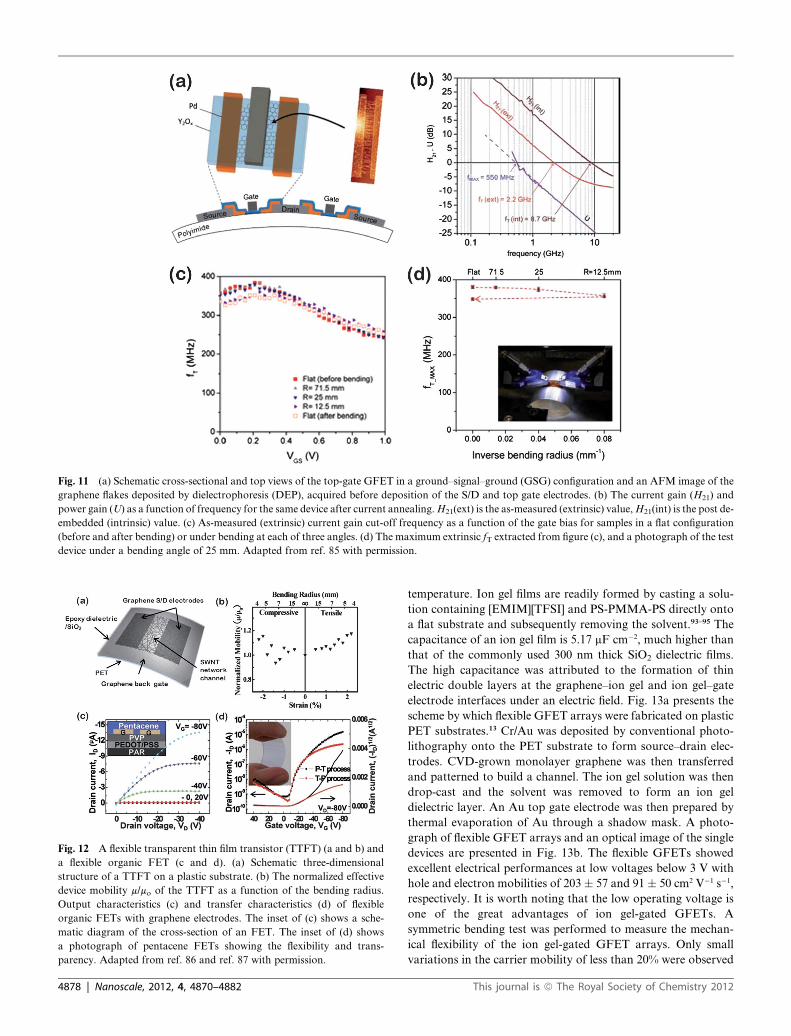
devices, as shown in Fig. 11. Top-gate solution-prepared GFETs
were fabricated on polyimide foils with a source–drain distance
of 260 nm, a gate length of 170 nm, and a gate width of 40 mm
(Fig. 11a).85 The resulting flexible graphene transistors exhibited
Fig. 10 Three-dimensional schematic illustration (a) and cross-sectional
view (b) of a high-speed GFET with a Co2Si/Al2O3 core–shell nanowire
self-aligned top gate. In this device, the Co2Si/Al2O3 core–shell nanowire
defined the channel length, the 5 nm Al2O3 shell functioned as the gate
dielectric, the metallic Co2Si core functioned as the self-integrated local
gate, and the self-aligned platinum thin film pads functioned as source
and drain electrodes. (c) Schematic illustration of a graphene mixer
circuit. The critical design aspects include a top-gate graphene transistor
and two inductors connected to the gate and drain of the GFET. The
three distinct metal layers of the graphene integrated circuit are indicated
as M1, M2, and M3. A layer of 120 nm thick SiO2 was used as the
isolation spacer to electrically separate the inductors (M3) from the
underlying interconnects (M1 and M2). (d) Optical image of a completed
graphene mixer. Adapted from ref. 80 and ref. 84 with permission.
This journal is ª The Royal Society of Chemistry 2012
a current gain cut-off frequency (extrinsic fT) of 2.2 GHz and
a power gain cut-off frequency (fm) of 550 MHz. Bending tests of
the flexible RF devices revealed remarkable mechanical stability.
These successful demonstrations highlight the practical applica-
tions of GFETs with complex functionalities.
3.2 Graphene-based flexible and stretchable transistors
In addition to flexible radio frequency transistors, the advantages
of graphene’s outstanding mechanical properties have found use
in other flexible, stretchable electronics. Since the removal of the
bottleneck in the synthesis and transfer of large-area, high-
quality graphene, CVD-grown graphene films have shown
promise for the fabrication of large-array flexible, stretchable
transistors. Here, we describe recent advances in the preparation
of flexible, stretchable transistors based on CVD-grown gra-
phene as channels and/or electrodes.
An array of flexible field-effect transistors was fabricated on
a flexible PET substrate using CVD-grown graphene source–
drain electrodes and a single-walled carbon nanotube (SWNT)
semiconducting channel,86 as shown in Fig. 12a. This device
presented a mobility of 2 cm2 V�1 s�1, an on/off ratio of 100, and
robust mechanical bendability with small variations in the carrier
mobility under strains of up to 2.2% (Fig. 12b). The integration
of graphene and carbon nanotubes yielded devices with a high
optical transparency. The transmittance values through the
channel and source–drain regions, excluding the bare PET
substrate, were 91% and 81% at 550 nm, respectively. One of the
merits of graphene electrodes in CNT transistors is the negligible
contact resistance, which is an important factor that affects the
carrier mobility. Organic field-effect transistors with graphene
electrodes exhibit low contact resistances compared with metal
electrodes.87–89 The contact resistance between an organic active
layer and an electrode in a field-effect transistor can be estimated
using the transfer line method (TLM).90–92 High-performance
organic FETs composed of a PEDOT:PSS gate electrode,
a cross-linked polyvinylphenol (PVP) dielectric layer, a penta-
cene active channel, and graphene source–drain electrodes were
recently prepared. The device architecture and performance are
presented in Fig. 12c and d.87 A device with graphene electrodes
exhibited a carrier mobility of 0.54 � 0.04 cm2 V�1 s�1 and an on/
off ratio of 107, much higher than the values for devices with Au
electrodes (0.02 cm2 V�1 s�1). The mobility difference between the
two materials was attributed to the low contact resistance
between the pentacene and graphene electrodes (two orders of
magnitude lower than the contact resistance between pentacene
and Au electrodes). Devices fabricated on a flexible PET
substrate showed an average carrier mobility of 0.12 cm2 V�1 s�1.
Typical high-k gate dielectric insulators, such as Al2O3 and
HfO2, are not suitable for use in GFETs fabricated on flexible
plastic substrates because they require a high growth tempera-
ture. High-capacitance gate dielectric materials that display good
interfacial properties with graphene and can be processed at low
temperatures are required. Solution-processable ion gel gate
dielectrics were found to meet these requirements very well.
Ion gels can be prepared by the gelation of a triblock copoly-
PS) in an ionic liquid, 1-ethyl-3-methylimidazolium bis(tri-
fluoromethylsulfonyl)imide ([EMIM] [TFSI]) at room
Nanoscale, 2012, 4, 4870–4882 | 4877
Fig. 11 (a) Schematic cross-sectional and top views of the top-gate GFET in a ground–signal–ground (GSG) configuration and an AFM image of the
graphene flakes deposited by dielectrophoresis (DEP), acquired before deposition of the S/D and top gate electrodes. (b) The current gain (H21) and
power gain (U) as a function of frequency for the same device after current annealing.H21(ext) is the as-measured (extrinsic) value,H21(int) is the post de-
embedded (intrinsic) value. (c) As-measured (extrinsic) current gain cut-off frequency as a function of the gate bias for samples in a flat configuration
(before and after bending) or under bending at each of three angles. (d) The maximum extrinsic fT extracted from figure (c), and a photograph of the test
device under a bending angle of 25 mm. Adapted from ref. 85 with permission.
Fig. 12 A flexible transparent thin film transistor (TTFT) (a and b) and
a flexible organic FET (c and d). (a) Schematic three-dimensional
structure of a TTFT on a plastic substrate. (b) The normalized effective
device mobility m/mo of the TTFT as a function of the bending radius.
Output characteristics (c) and transfer characteristics (d) of flexible
organic FETs with graphene electrodes. The inset of (c) shows a sche-
matic diagram of the cross-section of an FET. The inset of (d) shows
a photograph of pentacene FETs showing the flexibility and trans-
parency. Adapted from ref. 86 and ref. 87 with permission.
4878 | Nanoscale, 2012, 4, 4870–4882
temperature. Ion gel films are readily formed by casting a solu-
tion containing [EMIM][TFSI] and PS-PMMA-PS directly onto
a flat substrate and subsequently removing the solvent.93–95 The
capacitance of an ion gel film is 5.17 mF cm�2, much higher than
that of the commonly used 300 nm thick SiO2 dielectric films.
The high capacitance was attributed to the formation of thin
electric double layers at the graphene–ion gel and ion gel–gate
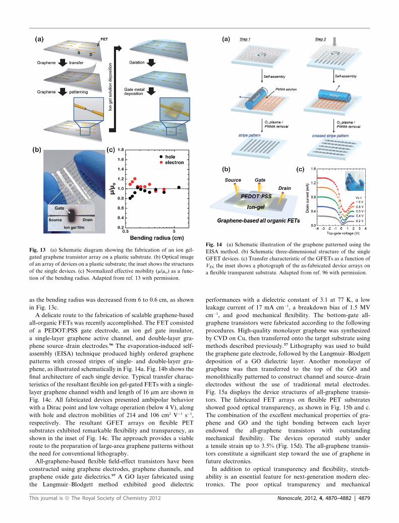
electrode interfaces under an electric field. Fig. 13a presents the
scheme by which flexible GFET arrays were fabricated on plastic
PET substrates.13 Cr/Au was deposited by conventional photo-
lithography onto the PET substrate to form source–drain elec-
trodes. CVD-grown monolayer graphene was then transferred
and patterned to build a channel. The ion gel solution was then
drop-cast and the solvent was removed to form an ion gel
dielectric layer. An Au top gate electrode was then prepared by
thermal evaporation of Au through a shadow mask. A photo-
graph of flexible GFET arrays and an optical image of the single
devices are presented in Fig. 13b. The flexible GFETs showed
excellent electrical performances at low voltages below 3 V with
hole and electron mobilities of 203 � 57 and 91 � 50 cm2 V�1 s�1,
respectively. It is worth noting that the low operating voltage is
one of the great advantages of ion gel-gated GFETs. A
symmetric bending test was performed to measure the mechan-
ical flexibility of the ion gel-gated GFET arrays. Only small
variations in the carrier mobility of less than 20% were observed
This journal is ª The Royal Society of Chemistry 2012
Fig. 13 (a) Schematic diagram showing the fabrication of an ion gel-
gated graphene transistor array on a plastic substrate. (b) Optical image
of an array of devices on a plastic substrate; the inset shows the structures
of the single devices. (c) Normalized effective mobility (m/mo) as a func-
tion of the bending radius. Adapted from ref. 13 with permission.
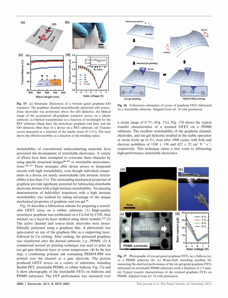
Fig. 14 (a) Schematic illustration of the graphene patterned using the
EISA method. (b) Schematic three-dimensional structure of the single
GFET devices. (c) Transfer characteristic of the GFETs as a function of
VD; the inset shows a photograph of the as-fabricated device arrays on
a flexible transparent substrate. Adapted from ref. 96 with permission.
as the bending radius was decreased from 6 to 0.6 cm, as shown
in Fig. 13c.
A delicate route to the fabrication of scalable graphene-based
all-organic FETs was recently accomplished. The FET consisted
of a PEDOT:PSS gate electrode, an ion gel gate insulator,
a single-layer graphene active channel, and double-layer gra-
phene source–drain electrodes.96 The evaporation-induced self-
assembly (EISA) technique produced highly ordered graphene
patterns with crossed stripes of single- and double-layer gra-
phene, as illustrated schematically in Fig. 14a. Fig. 14b shows the
final architecture of each single device. Typical transfer charac-
teristics of the resultant flexible ion gel-gated FETs with a single-
layer graphene channel width and length of 16 mm are shown in
Fig. 14c. All fabricated devices presented ambipolar behavior
with a Dirac point and low voltage operation (below 4 V), along
with hole and electron mobilities of 214 and 106 cm2 V�1 s�1,
respectively. The resultant GFET arrays on flexible PET
substrates exhibited remarkable flexibility and transparency, as
shown in the inset of Fig. 14c. The approach provides a viable
route to the preparation of large-area graphene patterns without
the need for conventional lithography.
All-graphene-based flexible field-effect transistors have been
constructed using graphene electrodes, graphene channels, and
graphene oxide gate dielectrics.97 A GO layer fabricated using
the Langmuir–Blodgett method exhibited good dielectric
This journal is ª The Royal Society of Chemistry 2012
performances with a dielectric constant of 3.1 at 77 K, a low
leakage current of 17 mA cm�1, a breakdown bias of 1.5 MV
cm�1, and good mechanical flexibility. The bottom-gate all-
graphene transistors were fabricated according to the following
procedures. High-quality monolayer graphene was synthesized
by CVD on Cu, then transferred onto the target substrate using
methods described previously.57 Lithography was used to build
the graphene gate electrode, followed by the Langmuir–Blodgett
deposition of a GO dielectric layer. Another monolayer of
graphene was then transferred to the top of the GO and
monolithically patterned to construct channel and source–drain
electrodes without the use of traditional metal electrodes.
Fig. 15a displays the device structures of all-graphene transis-
tors. The fabricated FET arrays on flexible PET substrates
showed good optical transparency, as shown in Fig. 15b and c.
The combination of the excellent mechanical properties of gra-
phene and GO and the tight bonding between each layer
endowed the all-graphene transistors with outstanding
mechanical flexibility. The devices operated stably under
a tensile strain up to 3.5% (Fig. 15d). The all-graphene transis-
tors constitute a significant step toward the use of graphene in
future electronics.
In addition to optical transparency and flexibility, stretch-
ability is an essential feature for next-generation modern elec-
tronics. The poor optical transparency and mechanical
Nanoscale, 2012, 4, 4870–4882 | 4879
Fig. 15 (a) Schematic illustration of a bottom gated graphene–GO
transistor. The graphene channel monolithically patterned with source–
drain electrodes was positioned above the GO dielectric. (b) Optical
image of the as-prepared all-graphene transistor arrays on a plastic
substrate. (c) Optical transmittance as a function of wavelength for the
PET substrate (black line), the monolayer graphene (red line), and the
GO dielectric (blue line) of a device on a PET substrate. (d) Transfer
curves measured as a function of the tensile strain (0–3.5%). The inset
shows the effective mobility as a function of the bending radius.
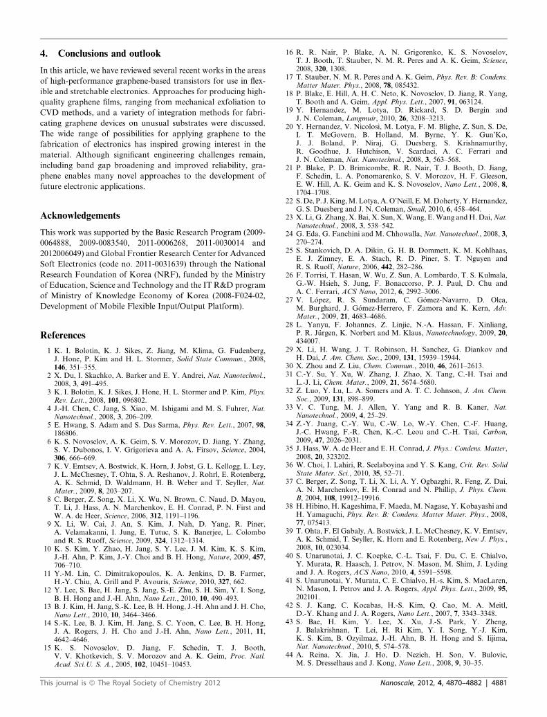
Fig. 16 Fabrication schematics of arrays of graphene FETs fabricated
on a stretchable substrate. Adapted from ref. 14 with permission.
Fig. 17 Photographs of ion gel-gated graphene FETs on a balloon (a),
or a PDMS substrate (b). (c) Home-built stretching machine for
measuring the electrical performance of the ion gel-gated graphene FETs
fabricated on stretchable PDMS substrates (with a thickness of 1.5 mm).
(d) Typical transfer characteristics of the strained graphene FETs on
PDMS. Adapted from ref. 14 with permission.
stretchability of conventional semiconducting materials have
prevented the development of stretchable electronics. A variety
of efforts have been attempted to overcome these obstacles by
using specific structural designs98–101 or stretchable interconnec-
tions.102–111 These strategies offer device arrays or integrated
circuits with high stretchability, even though individual compo-
nents in a device are nearly unstretchable (the intrinsic stretch-
ability is less than 1%). The outstanding mechanical properties of
graphene provide significant potential for fabricating stretchable
electronic devices with a high intrinsic stretchability. An amazing
demonstration of field-effect transistors with a high intrinsic
stretchability was realized by taking advantage of the unique
mechanical properties of graphene and ion gel.14
Fig. 16 describes a fabrication scheme for preparing a stretch-
able GFET array on a rubber substrate. (1) High-quality
monolayer graphene was synthesized on a Cu foil by CVD, then
stacked via a layer-by-layer method using direct transfer.112 (2)
The active channel and source–drain electrodes were mono-
lithically patterned using a graphene film. A photoresist was
spin-coated on top of the graphene film as a supporting layer,
followed by Cu etching. After etching, the patterned graphene
was transferred onto the desired substrate, e.g., PDMS. (3) A
commercial aerosol jet printing technique was used to print an
ion gel gate dielectric layer at room temperature. (4) In the last
step, a conducting polymer ink containing PEDOT:PSS was
printed over the channel as a gate electrode. The process
produced GFET arrays on a variety of substrates, including
flexible PET, stretchable PDMS, or rubber balloon. Fig. 17a and
b show photographs of the stretchable FETs on balloons and
PDMS substrates. The FET performance was measured over
4880 | Nanoscale, 2012, 4, 4870–4882
a strain range of 0–7% (Fig. 17c). Fig. 17d shows the typical
transfer characteristics of a strained GFET on a PDMS
substrate. The excellent stretchability of the graphene channel,
electrodes, and ion gel dielectric resulted in the stable operation
at strain levels up to 5%, even after 1000 cycles, with hole and
electron mobilities of 1188 � 136 and 422 � 52 cm2 V�1 s�1,
respectively. This technique opens a new route to fabricating
high-performance stretchable electronics.
This journal is ª The Royal Society of Chemistry 2012
4. Conclusions and outlook
In this article, we have reviewed several recent works in the areas
of high-performance graphene-based transistors for use in flex-
ible and stretchable electronics. Approaches for producing high-
quality graphene films, ranging from mechanical exfoliation to
CVD methods, and a variety of integration methods for fabri-
cating graphene devices on unusual substrates were discussed.
The wide range of possibilities for applying graphene to the
fabrication of electronics has inspired growing interest in the
material. Although significant engineering challenges remain,
including band gap broadening and improved reliability, gra-
phene enables many novel approaches to the development of
future electronic applications.
Acknowledgements
This work was supported by the Basic Research Program (2009-
0064888, 2009-0083540, 2011-0006268, 2011-0030014 and
2012006049) and Global Frontier Research Center for Advanced
Soft Electronics (code no. 2011-0031639) through the National
Research Foundation of Korea (NRF), funded by the Ministry
of Education, Science and Technology and the IT R&D program
of Ministry of Knowledge Economy of Korea (2008-F024-02,
Development of Mobile Flexible Input/Output Platform).
References
1 K. I. Bolotin, K. J. Sikes, Z. Jiang, M. Klima, G. Fudenberg,J. Hone, P. Kim and H. L. Stormer, Solid State Commun., 2008,146, 351–355.
2 X. Du, I. Skachko, A. Barker and E. Y. Andrei, Nat. Nanotechnol.,2008, 3, 491–495.
3 K. I. Bolotin, K. J. Sikes, J. Hone, H. L. Stormer and P. Kim, Phys.Rev. Lett., 2008, 101, 096802.
4 J.-H. Chen, C. Jang, S. Xiao, M. Ishigami and M. S. Fuhrer, Nat.Nanotechnol., 2008, 3, 206–209.
5 E. Hwang, S. Adam and S. Das Sarma, Phys. Rev. Lett., 2007, 98,186806.
6 K. S. Novoselov, A. K. Geim, S. V. Morozov, D. Jiang, Y. Zhang,S. V. Dubonos, I. V. Grigorieva and A. A. Firsov, Science, 2004,306, 666–669.
7 K. V. Emtsev, A. Bostwick, K. Horn, J. Jobst, G. L. Kellogg, L. Ley,J. L. McChesney, T. Ohta, S. A. Reshanov, J. Rohrl, E. Rotenberg,A. K. Schmid, D. Waldmann, H. B. Weber and T. Seyller, Nat.Mater., 2009, 8, 203–207.
8 C. Berger, Z. Song, X. Li, X. Wu, N. Brown, C. Naud, D. Mayou,T. Li, J. Hass, A. N. Marchenkov, E. H. Conrad, P. N. First andW. A. de Heer, Science, 2006, 312, 1191–1196.
9 X. Li, W. Cai, J. An, S. Kim, J. Nah, D. Yang, R. Piner,A. Velamakanni, I. Jung, E. Tutuc, S. K. Banerjee, L. Colomboand R. S. Ruoff, Science, 2009, 324, 1312–1314.
10 K. S. Kim, Y. Zhao, H. Jang, S. Y. Lee, J. M. Kim, K. S. Kim,J.-H. Ahn, P. Kim, J.-Y. Choi and B. H. Hong, Nature, 2009, 457,706–710.
11 Y.-M. Lin, C. Dimitrakopoulos, K. A. Jenkins, D. B. Farmer,H.-Y. Chiu, A. Grill and P. Avouris, Science, 2010, 327, 662.
12 Y. Lee, S. Bae, H. Jang, S. Jang, S.-E. Zhu, S. H. Sim, Y. I. Song,B. H. Hong and J.-H. Ahn, Nano Lett., 2010, 10, 490–493.
13 B. J. Kim, H. Jang, S.-K. Lee, B. H. Hong, J.-H. Ahn and J. H. Cho,Nano Lett., 2010, 10, 3464–3466.
14 S.-K. Lee, B. J. Kim, H. Jang, S. C. Yoon, C. Lee, B. H. Hong,J. A. Rogers, J. H. Cho and J.-H. Ahn, Nano Lett., 2011, 11,4642–4646.
15 K. S. Novoselov, D. Jiang, F. Schedin, T. J. Booth,V. V. Khotkevich, S. V. Morozov and A. K. Geim, Proc. Natl.Acad. Sci.U. S. A., 2005, 102, 10451–10453.
This journal is ª The Royal Society of Chemistry 2012
16 R. R. Nair, P. Blake, A. N. Grigorenko, K. S. Novoselov,T. J. Booth, T. Stauber, N. M. R. Peres and A. K. Geim, Science,2008, 320, 1308.
17 T. Stauber, N. M. R. Peres and A. K. Geim, Phys. Rev. B: Condens.Matter Mater. Phys., 2008, 78, 085432.
18 P. Blake, E. Hill, A. H. C. Neto, K. Novoselov, D. Jiang, R. Yang,T. Booth and A. Geim, Appl. Phys. Lett., 2007, 91, 063124.
19 Y. Hernandez, M. Lotya, D. Rickard, S. D. Bergin andJ. N. Coleman, Langmuir, 2010, 26, 3208–3213.
20 Y. Hernandez, V. Nicolosi, M. Lotya, F. M. Blighe, Z. Sun, S. De,I. T. McGovern, B. Holland, M. Byrne, Y. K. Gun’Ko,J. J. Boland, P. Niraj, G. Duesberg, S. Krishnamurthy,R. Goodhue, J. Hutchison, V. Scardaci, A. C. Ferrari andJ. N. Coleman, Nat. Nanotechnol., 2008, 3, 563–568.
21 P. Blake, P. D. Brimicombe, R. R. Nair, T. J. Booth, D. Jiang,F. Schedin, L. A. Ponomarenko, S. V. Morozov, H. F. Gleeson,E. W. Hill, A. K. Geim and K. S. Novoselov, Nano Lett., 2008, 8,1704–1708.
22 S.De, P. J.King,M.Lotya,A.O’Neill, E.M.Doherty,Y.Hernandez,G. S. Duesberg and J. N. Coleman, Small, 2010, 6, 458–464.
24 G. Eda, G. Fanchini and M. Chhowalla, Nat. Nanotechnol., 2008, 3,270–274.
25 S. Stankovich, D. A. Dikin, G. H. B. Dommett, K. M. Kohlhaas,E. J. Zimney, E. A. Stach, R. D. Piner, S. T. Nguyen andR. S. Ruoff, Nature, 2006, 442, 282–286.
26 F. Torrisi, T. Hasan, W. Wu, Z. Sun, A. Lombardo, T. S. Kulmala,G.-W. Hsieh, S. Jung, F. Bonaccorso, P. J. Paul, D. Chu andA. C. Ferrari, ACS Nano, 2012, 6, 2992–3006.
27 V. L�opez, R. S. Sundaram, C. G�omez-Navarro, D. Olea,M. Burghard, J. G�omez-Herrero, F. Zamora and K. Kern, Adv.Mater., 2009, 21, 4683–4686.
28 L. Yanyu, F. Johannes, Z. Linjie, N.-A. Hassan, F. Xinliang,P. R. J€urgen, K. Norbert and M. Klaus, Nanotechnology, 2009, 20,434007.
29 X. Li, H. Wang, J. T. Robinson, H. Sanchez, G. Diankov andH. Dai, J. Am. Chem. Soc., 2009, 131, 15939–15944.
30 X. Zhou and Z. Liu, Chem. Commun., 2010, 46, 2611–2613.31 C.-Y. Su, Y. Xu, W. Zhang, J. Zhao, X. Tang, C.-H. Tsai and
L.-J. Li, Chem. Mater., 2009, 21, 5674–5680.32 Z. Luo, Y. Lu, L. A. Somers and A. T. C. Johnson, J. Am. Chem.
Soc., 2009, 131, 898–899.33 V. C. Tung, M. J. Allen, Y. Yang and R. B. Kaner, Nat.
35 J. Hass, W. A. de Heer and E. H. Conrad, J. Phys.: Condens. Matter,2008, 20, 323202.
36 W. Choi, I. Lahiri, R. Seelaboyina and Y. S. Kang, Crit. Rev. SolidState Mater. Sci., 2010, 35, 52–71.
37 C. Berger, Z. Song, T. Li, X. Li, A. Y. Ogbazghi, R. Feng, Z. Dai,A. N. Marchenkov, E. H. Conrad and N. Phillip, J. Phys. Chem.B, 2004, 108, 19912–19916.
38 H. Hibino, H. Kageshima, F. Maeda, M. Nagase, Y. Kobayashi andH. Yamaguchi, Phys. Rev. B: Condens. Matter Mater. Phys., 2008,77, 075413.
39 T. Ohta, F. El Gabaly, A. Bostwick, J. L. McChesney, K. V. Emtsev,A. K. Schmid, T. Seyller, K. Horn and E. Rotenberg, New J. Phys.,2008, 10, 023034.
40 S. Unarunotai, J. C. Koepke, C.-L. Tsai, F. Du, C. E. Chialvo,Y. Murata, R. Haasch, I. Petrov, N. Mason, M. Shim, J. Lydingand J. A. Rogers, ACS Nano, 2010, 4, 5591–5598.
41 S. Unarunotai, Y. Murata, C. E. Chialvo, H.-s. Kim, S. MacLaren,N. Mason, I. Petrov and J. A. Rogers, Appl. Phys. Lett., 2009, 95,202101.
42 S. J. Kang, C. Kocabas, H.-S. Kim, Q. Cao, M. A. Meitl,D.-Y. Khang and J. A. Rogers, Nano Lett., 2007, 7, 3343–3348.
43 S. Bae, H. Kim, Y. Lee, X. Xu, J.-S. Park, Y. Zheng,J. Balakrishnan, T. Lei, H. Ri Kim, Y. I. Song, Y.-J. Kim,K. S. Kim, B. Ozyilmaz, J.-H. Ahn, B. H. Hong and S. Iijima,Nat. Nanotechnol., 2010, 5, 574–578.
44 A. Reina, X. Jia, J. Ho, D. Nezich, H. Son, V. Bulovic,M. S. Dresselhaus and J. Kong, Nano Lett., 2008, 9, 30–35.
Nanoscale, 2012, 4, 4870–4882 | 4881
45 Z. Peng, Z. Yan, Z. Sun and J. M. Tour, ACS Nano, 2011, 5, 8241–8247.
46 Z. Yan, Z. Peng, Z. Sun, J. Yao, Y. Zhu, Z. Liu, P. M. Ajayan andJ. M. Tour, ACS Nano, 2011, 5, 8187–8192.
47 S. Lee, K. Lee and Z. Zhong, Nano Lett., 2010, 10, 4702–4707.48 X. Li, C. W. Magnuson, A. Venugopal, J. An, J. W. Suk, B. Han,
M. Borysiak, W. Cai, A. Velamakanni, Y. Zhu, L. Fu,E. M. Vogel, E. Voelkl, L. Colombo and R. S. Ruoff, Nano Lett.,2010, 10, 4328–4334.
49 W. Wu, L. A. Jauregui, Z. Su, Z. Liu, J. Bao, Y. P. Chen and Q. Yu,Adv. Mater., 2011, 23, 4898–4903.
50 Z. Sun, Z. Yan, J. Yao, E. Beitler, Y. Zhu and J. M. Tour, Nature,2010, 468, 549–552.
51 W. Cai, Y. Zhu, X. Li, R. D. Piner and R. S. Ruoff, Appl. Phys.Lett., 2009, 95, 123115.
52 A. Srivastava, C. Galande, L. Ci, L. Song, C. Rai, D. Jariwala,K. F. Kelly and P. M. Ajayan, Chem. Mater., 2010, 22, 3457–3461.
53 Y. Wang, Y. Zheng, X. Xu, E. Dubuisson, Q. Bao, J. Lu andK. P. Loh, ACS Nano, 2011, 5, 9927–9933.
54 W. Regan, N. Alem, B. Aleman, B. Geng, C. Girit, L. Maserati,F.Wang,M.Crommie andA.Zettl,Appl.Phys.Lett., 2010,96, 113102.
55 V. P. Verma, S. Das, I. Lahiri and W. Choi, Appl. Phys. Lett., 2010,96, 203108.
56 E. H. Lock, M. Baraket, M. Laskoski, S. P. Mulvaney, W. K. Lee,P. E. Sheehan, D. R. Hines, J. T. Robinson, J. Tosado,M. S. Fuhrer, S. C. Hern�andez and S. G. Walton, Nano Lett.,2011, 12, 102–107.
57 X. Li, Y. Zhu, W. Cai, M. Borysiak, B. Han, D. Chen, R. D. Piner,L. Colombo and R. S. Ruoff, Nano Lett., 2009, 9, 4359–4363.
58 V. G. Kravets, A. N. Grigorenko, R. R. Nair, P. Blake,S. Anissimova, K. S. Novoselov and A. K. Geim, Phys. Rev. B:Condens. Matter Mater. Phys., 2010, 81, 155413.
59 K. Nomura and A. H. MacDonald, Phys. Rev. Lett., 2006, 96,256602.
60 J. C. Meyer, A. K. Geim, M. I. Katsnelson, K. S. Novoselov,T. J. Booth and S. Roth, Nature, 2007, 446, 60–63.
61 O. V. Yazyev and S. G. Louie, Nat. Mater., 2010, 9, 806–809.62 D. Wei, Y. Liu, Y. Wang, H. Zhang, L. Huang and G. Yu, Nano
Lett., 2009, 9, 1752–1758.63 H. Cao, Q. Yu, L. A. Jauregui, J. Tian, W. Wu, Z. Liu, R. Jalilian,
D. K. Benjamin, Z. Jiang, J. Bao, S. S. Pei and Y. P. Chen, Appl.Phys. Lett., 2010, 96, 122106.
64 C. Dean, A. Young, I. Meric, C. Lee, L. Wang, S. Sorgenfrei,K. Watanabe, T. Taniguchi, P. Kim and K. Shepard, Nat.Nanotechnol., 2010, 5, 722–726.
65 Z. Liu, L. Song, S. Zhao, J. Huang, L. Ma, J. Zhang, J. Lou andP. M. Ajayan, Nano Lett., 2011, 11, 2032–2037.
66 K. K. Kim, A. Hsu, X. Jia, S. M. Kim, Y. Shi, M. Hofmann,D. Nezich, J. F. Rodriguez-Nieva, M. Dresselhaus, T. Palaciosand J. Kong, Nano Lett., 2011, 12, 161–166.
67 K. H. Lee, H.-J. Shin, J. Lee, I.-y. Lee, G.-H. Kim, J.-Y. Choi andS.-W. Kim, Nano Lett., 2012, 12, 714–718.
68 Y. Shi, C. Hamsen, X. Jia, K. K. Kim, A. Reina, M. Hofmann,A. L. Hsu, K. Zhang, H. Li, Z.-Y. Juang, M. S. Dresselhaus,L.-J. Li and J. Kong, Nano Lett., 2010, 10, 4134–4139.
69 P. Sutter, J. Lahiri, P. Albrecht and E. Sutter, ACS Nano, 2011, 5,7303–7309.
70 L. Song, L. Ci, H. Lu, P. B. Sorokin, C. Jin, J. Ni, A. G. Kvashnin,D. G. Kvashnin, J. Lou, B. I. Yakobson and P. M. Ajayan, NanoLett., 2010, 10, 3209–3215.
71 K. Kim, J. Y. Choi, T. Kim, S. H. Cho and H. J. Chung, Nature,2011, 479, 338–344.
72 T. Ohta, A. Bostwick, T. Seyller, K. Horn and E. Rotenberg,Science, 2006, 313, 951–954.
73 M. Y. Han, B. €Ozyilmaz, Y. Zhang and P. Kim, Phys. Rev. Lett.,2007, 98, 206805.
74 X. Li, X. Wang, L. Zhang, S. Lee and H. Dai, Science, 2008, 319,1229–1232.
75 Z. H. Ni, T. Yu, Y. H. Lu, Y. Y. Wang, Y. P. Feng and Z. X. Shen,ACS Nano, 2008, 2, 2301–2305.
76 P. Avouris, Nano Lett., 2010, 10, 4285–4294.77 F. Schwierz, Nat. Nanotechnol., 2010, 5, 487–496.78 I. Meric, N. Baklitskaya, P. Kim and K. L. Shepard, Transistors,
IEEE International Electron Devices Meeting, 2008, IEDMTechnical Digest, 2008, pp. 1–4.
4882 | Nanoscale, 2012, 4, 4870–4882
79 Y.-M. Lin, K. A. Jenkins, A. Valdes-Garcia, J. P. Small,D. B. Farmer and P. Avouris, Nano Lett., 2009, 9, 422–426.
80 L. Liao, Y.-C. Lin, M. Bao, R. Cheng, J. Bai, Y. Liu, Y. Qu,K. L. Wang, Y. Huang and X. Duan, Nature, 2010, 467, 305–308.
81 L. Liao, J. Bai, R. Cheng, Y.-C. Lin, S. Jiang, Y. Qu, Y. Huang andX. Duan, Nano Lett., 2010, 10, 3952–3956.
82 S. Adam, E. H. Hwang, V. M. Galitski and S. Das Sarma, Proc.Natl. Acad. Sci. U. S. A., 2007, 104, 18392–18397.
83 J. A. Robinson, M. LaBella, M. Zhu, M. Hollander, R. Kasarda,Z. Hughes, K. Trumbull, R. Cavalero and D. Snyder, Appl. Phys.Lett., 2011, 98, 053103.
84 Y.-M. Lin, A. Valdes-Garcia, S.-J. Han, D. B. Farmer, I. Meric,Y. Sun, Y. Wu, C. Dimitrakopoulos, A. Grill, P. Avouris andK. A. Jenkins, Science, 2011, 332, 1294–1297.
85 C. Sire, F. Ardiaca, S. Lepilliet, J.-W. T. Seo, M. C. Hersam,G. Dambrine, H. Happy and V. Derycke, Nano Lett., 2012, 12,1184–1188.
86 J. Sukjae, et al., Nanotechnology, 2010, 21, 425201.87 W. H. Lee, J. Park, S. H. Sim, S. B. Jo, K. S. Kim, B. H. Hong and
K. Cho, Adv. Mater., 2011, 23, 1752–1756.88 H. c. A. Becerril, R. M. Stoltenberg, M. L. Tang, M. E. Roberts,
Z. Liu, Y. Chen, D. H. Kim, B.-L. Lee, S. Lee and Z. Bao, ACSNano, 2010, 4, 6343–6352.
89 J. H. Chen, M. Ishigami, C. Jang, D. R. Hines, M. S. Fuhrer andE. D. Williams, Adv. Mater., 2007, 19, 3623–3627.
90 D. Gundlach, L. Zhou, J. Nichols, T. Jackson, P. Necliudov andM. Shur, J. Appl. Phys., 2006, 100, 024509.
91 P. V. Necliudov, M. S. Shur, D. J. Gundlach and T. N. Jackson,Solid-State Electron., 2003, 47, 259–262.
92 H. Klauk, G. Schmid,W. Radlik,W.Weber, L. Zhou, C. D. Sheraw,J. A. Nichols and T. N. Jackson, Solid-State Electron., 2003, 47, 297–301.
93 J. H. Cho, J. Lee, Y. He, B. S. Kim, T. P. Lodge and C. D. Frisbie,Adv. Mater., 2008, 20, 686–690.
94 J. H. Cho, J. Lee, Y. Xia, B. Kim, Y. He, M. J. Renn, T. P. Lodgeand C. Daniel Frisbie, Nat. Mater., 2008, 7, 900–906.
95 J. Lee, L. G. Kaake, J. H. Cho, X. Y. Zhu, T. P. Lodge andC. D. Frisbie, J. Phys. Chem. C, 2009, 113, 8972–8981.
96 T. Kim, H. Kim, S. W. Kwon, Y. Kim, W. K. Park, D. H. Yoon,A. R. Jang, H. S. Shin, K. S. Suh and W. S. Yang, Nano Lett.,2012, 12, 743–748.
97 S.-K. Lee, H. Y. Jang, S. Jang, E. Choi, B. H. Hong, J. Lee, S. Parkand J.-H. Ahn, Nano Lett., 2012, DOI: 10.1021/nl300948c.
98 D. H. Kim, J. H. Ahn, W. M. Choi, H. S. Kim, T. H. Kim, J. Song,Y. Y. Huang, Z. Liu, C. Lu and J. A. Rogers, Science, 2008, 320,507.
99 J. A. Rogers and Y. Huang, Proc. Natl. Acad. Sci. U. S. A., 2009,106, 10875–10876.
100 J. A. Rogers, T. Someya and Y. Huang, Science, 2010, 327, 1603–1607.
101 D. Brosteaux, F. Axisa, M. Gonzalez and J. Vanfleteren, IEEEElectron Device Lett., 2007, 28, 552–554.
102 A. C. Siegel, D. A. Bruzewicz, D. B. Weibel and G. M. Whitesides,Adv. Mater., 2007, 19, 727–733.
103 T. S. Hansen, K. West, O. Hassager and N. B. Larsen, Adv. Funct.Mater., 2007, 17, 3069–3073.
104 T. Sekitani, Y. Noguchi, K. Hata, T. Fukushima, T. Aida andT. Someya, Science, 2008, 321, 1468.
105 K.-Y. Chun, Y. Oh, J. Rho, J.-H. Ahn, Y.-J. Kim, H. R. Choi andS. Baik, Nat. Nanotechnol., 2010, 5, 853–857.
106 J. Jones, S. P. Lacour, S. Wagner and Z. Suo, J. Vac. Sci. Technol.,A, 2004, 22, 1723–1725.
107 T. Adrega and S. P. Lacour, J. Micromech. Microeng., 2010, 20,055025.
108 F. N. Ishikawa, H.-k. Chang, K. Ryu, P.-c. Chen, A. Badmaev,L. Gomez De Arco, G. Shen and C. Zhou, ACS Nano, 2009, 3,73–79.
109 K. Nogi, M. Hosokawa, M. Naito and T. Yokoyama, NanoparticleTechnology Handbook, Elsevier Science, 2007.
110 B. Y. Ahn, E. B. Duoss, M. J. Motala, X. Guo, S.-I. Park, Y. Xiong,J. Yoon, R. G. Nuzzo, J. A. Rogers and J. A. Lewis, Science, 2009,323, 1590–1593.
111 D.-H. Kim and J. A. Rogers, ACS Nano, 2009, 3, 498–501.112 Y. Wang, S. W. Tong, X. F. Xu, B. €Ozyilmaz and K. P. Loh, Adv.
Mater., 2011, 23, 1514–1518.
This journal is ª The Royal Society of Chemistry 2012