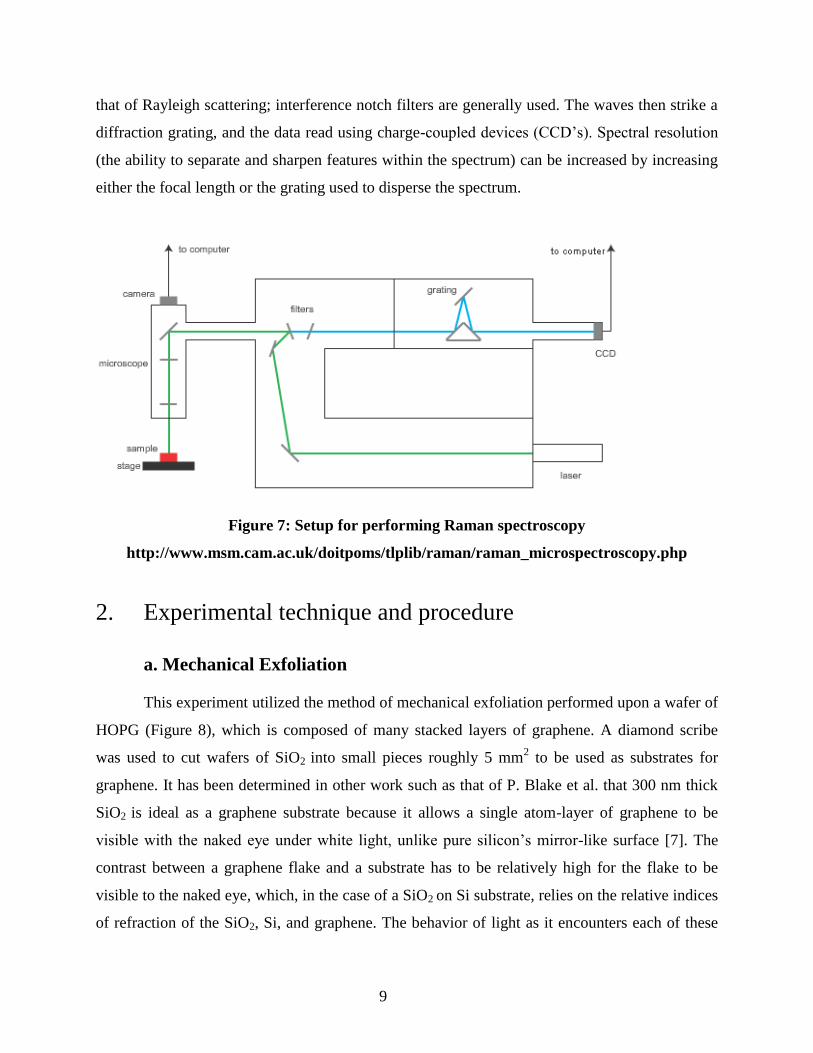
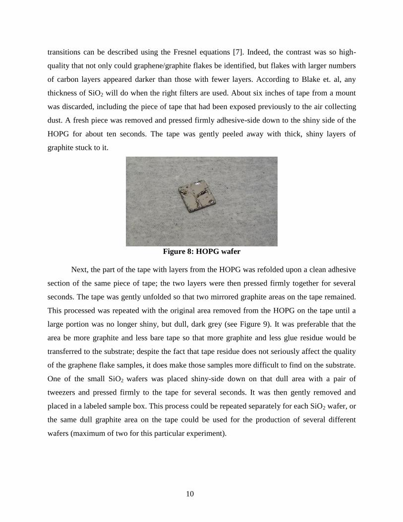
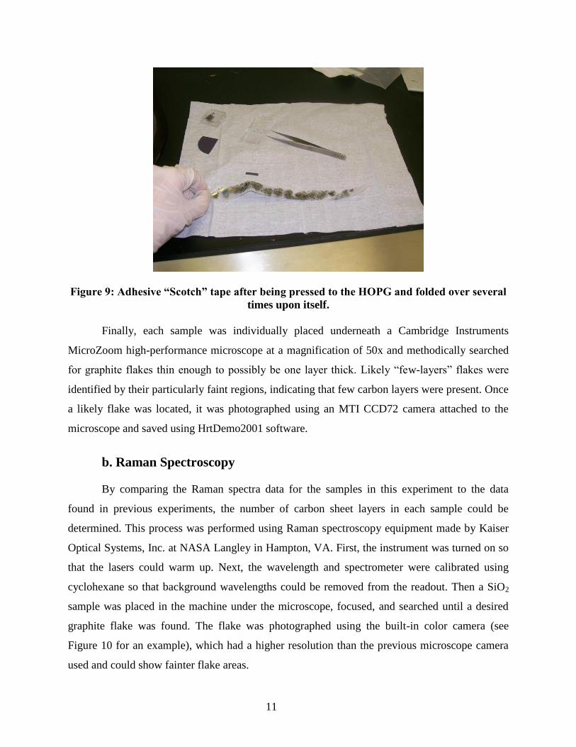
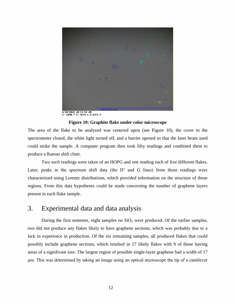
1 Graphene: Characterization After Mechanical Exfoliation Charlotte Reeves Research Advisor: R. A. Lukaszew April, 2010 Abstract The purpose of this experiment was to produce and characterize samples of graphene, defined as a one-atom layer of hexagonally bonded carbon atoms, using a method of mechanical exfoliation. This was done by following the work of K. S. Novoselov in the group of A. K. Geim at the University of Manchester (2004) using Scotch tape to pull apart the layers of a piece of highly oriented pyrolytic graphite (HOPG) and transfer layers from the graphite onto a SiO 2 substrate. These samples were then inspected using an optical microscope in an attempt to discover any thin flakes that might contain sections of single-layer graphene. Nine thin flakes with lengths up to 17 μm were determined to be likely candidates, and two of these plus three others were analyzed using Raman spectroscopy at NASA Langley using a laser of wavelength 532 nm. From these it was determined that a graphene flake two atomic layers thick had been produced. 1. Introduction and Theory Overview a. An overview of graphene Nature has produced 3-D materials such as graphite which are composed of many stacked layers of 2-D planar materials. In general, 2-D materials are rarely found in nature because of their instability; thin films, for instance, can become thermodynamically unstable and decompose or segregate below a certain thickness, and in other materials single layers appear only as transient states [1]. Graphene, however, is a notable exception. Graphene is defined as a single one-atom layer of hexagonally bonded carbon atoms (see Figure 1), while graphite is composed of many stacked graphene layers [2].
Transcript
1
Graphene: Characterization After Mechanical Exfoliation
Charlotte Reeves
Research Advisor: R. A. Lukaszew
April, 2010
Abstract
The purpose of this experiment was to produce and characterize samples
of graphene, defined as a one-atom layer of hexagonally bonded carbon atoms,
using a method of mechanical exfoliation. This was done by following the work
of K. S. Novoselov in the group of A. K. Geim at the University of Manchester
(2004) using Scotch tape to pull apart the layers of a piece of highly oriented
pyrolytic graphite (HOPG) and transfer layers from the graphite onto a SiO2
substrate. These samples were then inspected using an optical microscope in an
attempt to discover any thin flakes that might contain sections of single-layer
graphene. Nine thin flakes with lengths up to 17 μm were determined to be likely
candidates, and two of these plus three others were analyzed using Raman
spectroscopy at NASA Langley using a laser of wavelength 532 nm. From these it
was determined that a graphene flake two atomic layers thick had been produced.
1. Introduction and Theory Overview
a. An overview of graphene
Nature has produced 3-D materials such as graphite which are composed of many stacked
layers of 2-D planar materials. In general, 2-D materials are rarely found in nature because of
their instability; thin films, for instance, can become thermodynamically unstable and decompose
or segregate below a certain thickness, and in other materials single layers appear only as
transient states [1]. Graphene, however, is a notable exception. Graphene is defined as a single
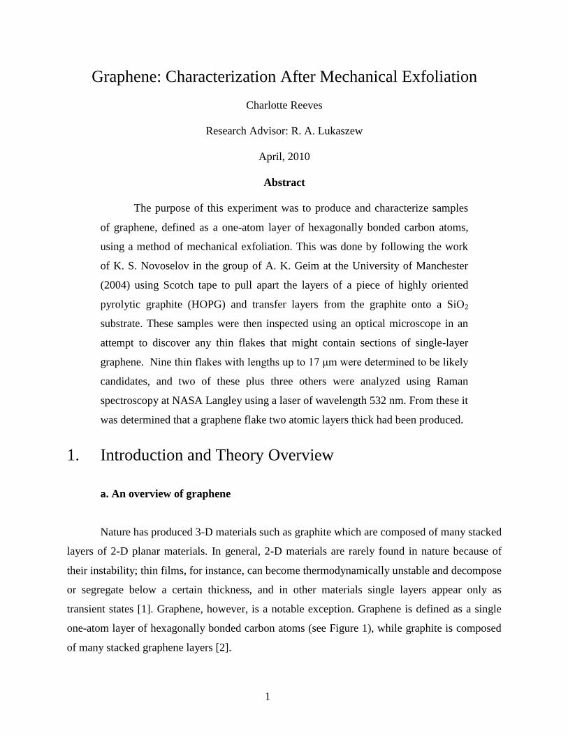
one-atom layer of hexagonally bonded carbon atoms (see Figure 1), while graphite is composed
of many stacked graphene layers [2].
2
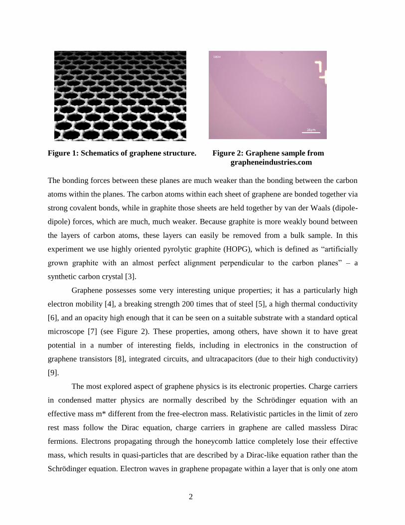
Figure 1: Schematics of graphene structure. Figure 2: Graphene sample from
grapheneindustries.com
The bonding forces between these planes are much weaker than the bonding between the carbon
atoms within the planes. The carbon atoms within each sheet of graphene are bonded together via
strong covalent bonds, while in graphite those sheets are held together by van der Waals (dipole-
dipole) forces, which are much, much weaker. Because graphite is more weakly bound between
the layers of carbon atoms, these layers can easily be removed from a bulk sample. In this
experiment we use highly oriented pyrolytic graphite (HOPG), which is defined as “artificially
grown graphite with an almost perfect alignment perpendicular to the carbon planes” – a
synthetic carbon crystal [3].
Graphene possesses some very interesting unique properties; it has a particularly high
electron mobility [4], a breaking strength 200 times that of steel [5], a high thermal conductivity
[6], and an opacity high enough that it can be seen on a suitable substrate with a standard optical
microscope [7] (see Figure 2). These properties, among others, have shown it to have great
potential in a number of interesting fields, including in electronics in the construction of
graphene transistors [8], integrated circuits, and ultracapacitors (due to their high conductivity)
[9].
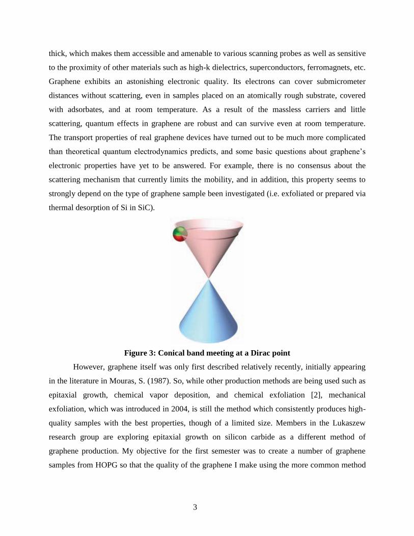
The most explored aspect of graphene physics is its electronic properties. Charge carriers
in condensed matter physics are normally described by the Schrödinger equation with an
effective mass m* different from the free-electron mass. Relativistic particles in the limit of zero
rest mass follow the Dirac equation, charge carriers in graphene are called massless Dirac
fermions. Electrons propagating through the honeycomb lattice completely lose their effective
mass, which results in quasi-particles that are described by a Dirac-like equation rather than the
Schrödinger equation. Electron waves in graphene propagate within a layer that is only one atom
3
thick, which makes them accessible and amenable to various scanning probes as well as sensitive
to the proximity of other materials such as high-k dielectrics, superconductors, ferromagnets, etc.
Graphene exhibits an astonishing electronic quality. Its electrons can cover submicrometer
distances without scattering, even in samples placed on an atomically rough substrate, covered
with adsorbates, and at room temperature. As a result of the massless carriers and little
scattering, quantum effects in graphene are robust and can survive even at room temperature.
The transport properties of real graphene devices have turned out to be much more complicated
than theoretical quantum electrodynamics predicts, and some basic questions about graphene’s
electronic properties have yet to be answered. For example, there is no consensus about the
scattering mechanism that currently limits the mobility, and in addition, this property seems to
strongly depend on the type of graphene sample been investigated (i.e. exfoliated or prepared via
thermal desorption of Si in SiC).
Figure 3: Conical band meeting at a Dirac point
However, graphene itself was only first described relatively recently, initially appearing
in the literature in Mouras, S. (1987). So, while other production methods are being used such as
epitaxial growth, chemical vapor deposition, and chemical exfoliation [2], mechanical
exfoliation, which was introduced in 2004, is still the method which consistently produces high-
quality samples with the best properties, though of a limited size. Members in the Lukaszew
research group are exploring epitaxial growth on silicon carbide as a different method of
graphene production. My objective for the first semester was to create a number of graphene
samples from HOPG so that the quality of the graphene I make using the more common method
4
of mechanical exfoliation can be compared to the graphene they produce using an alternative
method
b. An overview of Raman spectroscopy
Raman spectroscopy is one method currently used to determine how many layers of
graphene are present in a present sample. It utilizes the process of Raman scattering to identify
what materials are present in a specific sample by analyzing the shift in wavelength of light that
is scattered off of a material, which is different for different materials.
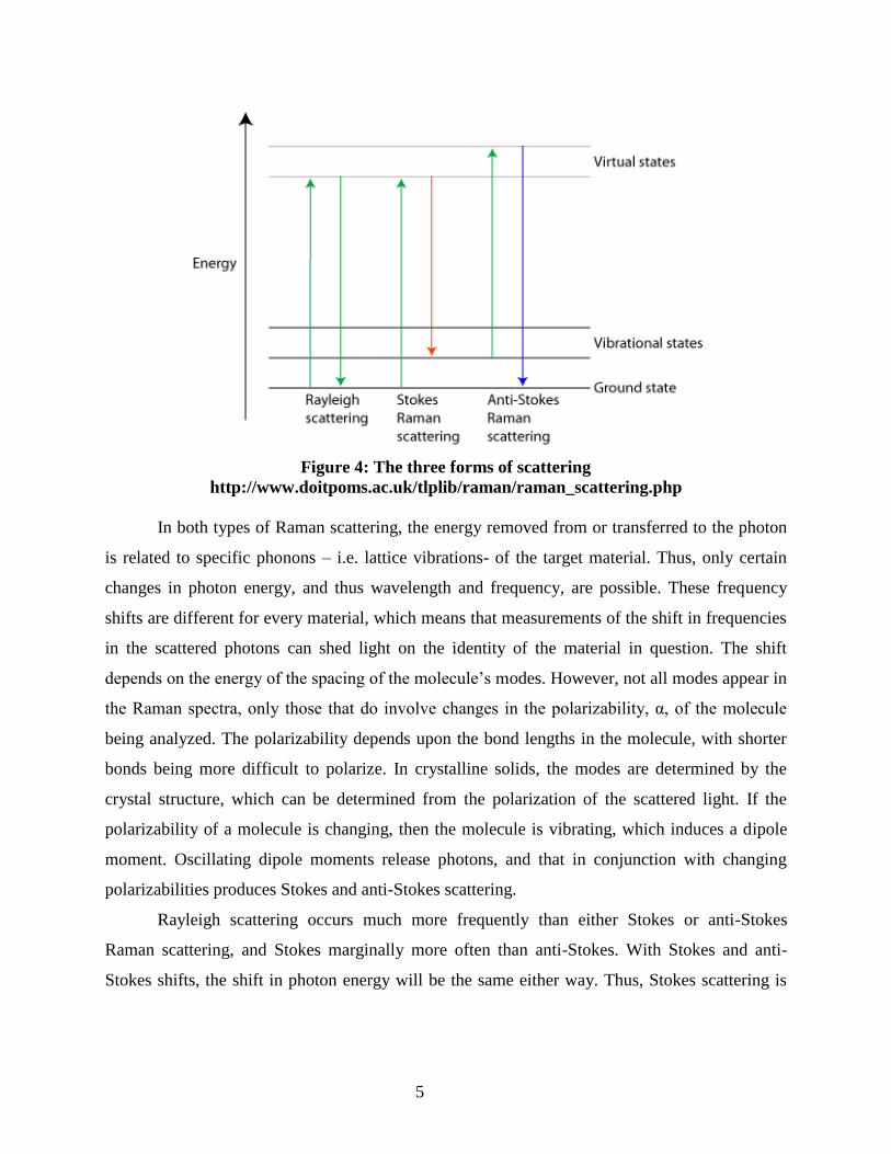
There are two primary types of scattering that occur when light strikes a material:
Rayleigh and Raman scattering. In Rayleigh scattering, a photon of a given energy and
wavelength interacts with a molecule in a material and raises it to a virtual energy state. After a
moment, the molecule comes back down to its original energy state, releasing another photon.
Since the molecule came back down to its original energy state after being raised, the released
photon has the same energy (and thus wavelength) as the incident photon; thus, Rayleigh
scattering can be referred to as an elastic process (the energy of the photon being conserved).
In Raman scattering, a photon of a given energy and wavelength also interacts with a
molecule in a material and raises it to a virtual energy state, as in Rayleigh scattering. However,
when the molecule drops from its virtual energy state, it may drop not to its original state but to a
state above or below its original energy state. When the molecule drops to a lower state it
releases a photon; however, the energy of the photon is not the same as that of the incident
photon. The energy of the released photon is dependent on the final energy state of the molecule.
If the final energy state of the molecule is greater than its original ground state, then the released
photon will have a lower energy than the incident photon, and thus a longer wavelength; this is
referred to as Stoke’s Raman scattering. However, if the final energy state of the molecule is
lower than the original initial state, then the released photon will have a higher energy than the
incident photon, and thus a shorter wavelength – anti-Stokes Raman scattering. Since the energy
of the photons is not conserved, Raman scattering is a form of inelastic scattering. See Figure 4
for a visual representation of all three types of scattering and the differences between their elastic