ARTICLE Received 19 Aug 2014 | Accepted 12 Feb 2015 | Published 20 Mar 2015 Graphene-enabled electrically switchable radar-absorbing surfaces Osman Balci 1 , Emre O. Polat 1 , Nurbek Kakenov 1 & Coskun Kocabas 1 Radar-absorbing materials are used in stealth technologies for concealment of an object from radar detection. Resistive and/or magnetic composite materials are used to reduce the backscattered microwave signals. Inability to control electrical properties of these materials, however, hinders the realization of active camouflage systems. Here, using large-area graphene electrodes, we demonstrate active surfaces that enable electrical control of reflection, transmission and absorption of microwaves. Instead of tuning bulk material property, our strategy relies on electrostatic tuning of the charge density on an atomically thin electrode, which operates as a tunable metal in microwave frequencies. Notably, we report large-area adaptive radar-absorbing surfaces with tunable reflection suppression ratio up to 50 dB with operation voltages o5V. Using the developed surfaces, we demonstrate various device architectures including pixelated and curved surfaces. Our results provide a significant step in realization of active camouflage systems in microwave frequencies. DOI: 10.1038/ncomms7628 1 Bilkent University, Department of Physics, 06800 Ankara, Turkey. Correspondence and requests for materials should be addressed to C.K. (email: [email protected]). NATURE COMMUNICATIONS | 6:6628 | DOI: 10.1038/ncomms7628 | www.nature.com/naturecommunications 1 & 2015 Macmillan Publishers Limited. All rights reserved.
Transcript
ARTICLE
Received 19 Aug 2014 | Accepted 12 Feb 2015 | Published 20 Mar 2015
Radar-absorbing materials are used in stealth technologies for concealment of an object from
radar detection. Resistive and/or magnetic composite materials are used to reduce the
backscattered microwave signals. Inability to control electrical properties of these materials,
however, hinders the realization of active camouflage systems. Here, using large-area
graphene electrodes, we demonstrate active surfaces that enable electrical control of
reflection, transmission and absorption of microwaves. Instead of tuning bulk material
property, our strategy relies on electrostatic tuning of the charge density on an atomically thin
electrode, which operates as a tunable metal in microwave frequencies. Notably, we report
large-area adaptive radar-absorbing surfaces with tunable reflection suppression ratio up to
50 dB with operation voltages o5 V. Using the developed surfaces, we demonstrate various
device architectures including pixelated and curved surfaces. Our results provide a significant
step in realization of active camouflage systems in microwave frequencies.
DOI: 10.1038/ncomms7628
1 Bilkent University, Department of Physics, 06800 Ankara, Turkey. Correspondence and requests for materials should be addressed to C.K.(email: [email protected]).
Microwaves are part of the electromagnetic spectrum withwavelengths of from one millimetre to a metre. Radarand communication technologies use passive metallic
surfaces to guide microwaves in the free space and resistivesurfaces to absorb them1,2. Although the source of microwavescan be controlled by electrical means, active control ofmicrowaves in the free space has been a challenge due to therequirement of large-area adaptive surfaces in microwavefrequencies3–8. Microwave analogues of smart optical windowsthat enable electrically tunable microwave reflection andtransmission have been the subject of active research for manydecades3,7,9. The key challenge is the ability to tune theinteraction between microwaves and matter by electrical means.These interactions are mainly governed by dielectric responseof the materials. Materials with tunable conductivity9,10,permittivity11 or permeability12,13 have been exploited foradaptive surfaces. Instead of controlling the bulk materialproperties, here we propose to control microwaves by tuningthe density of free charges on a surface. Large-area, the two-dimensional crystal of carbon, graphene, allows us to test thisapproach and fabricate a new class of adaptive microwavesurfaces14,15. One can confidently argue that an atomically thincoating has negligible effects on the reflection of microwaves froma surface unless there are abundant free charges on it. Throughelectrostatic doping, we show that atomically thin layers can beused as a switchable radar absorbing surfaces. Graphene andcarbon nanotube-based composite materials have been used asresistive materials to absorb microwaves; however, to ourknowledge they have not been used for active microwavesurfaces16–27.
Metals do not yield tunable electrical conductivity via externalelectric fields. This drawback prevents the uses of metals for
adaptive microwave surfaces. Semiconductors can yield tunablesurface charge density by means of metal-oxide semiconductorstructures28; however, the metallic gate electrode covers thesurface of semiconductor and screens the accumulated charges.Heating or illuminating a bare semiconductor surface with a lightsource can generate free carriers; but, these techniques are notpractical for realistic device configurations. Electrically tunablematerials such as ferroelectric materials29,30 and compositepolymers31,32 have been studied for possible active microwavesurfaces. Inability to fabricate these materials over large area andweak modulation of dielectric properties prevents realization ofadaptive microwave surfaces. Another approach is to usedistributed active circuit elements (diodes, transistors or photo-switches) integrated with passive metallic structures33,34. Externalbias voltage or light source applied on these distributed circuitelements changes the effective length of metallic structures, whichyield limited control over the reflectivity of the surface. Moreover,micro-electro-mechanical devices and mechanical actuators havebeen used to control microwaves by mechanical means35,36.Recently, graphene provides new perspective to realize adaptivesurfaces. The ability to control charge density on grapheneenables new active terahertz devices for various applicationssuch as switches37, modulators38–42, metamaterials43–45,plasmonics44,46 and cloaking43,47. A review by Sensale–Rodrigues et al.48 summarizes these recent developments inreconfigurable terahertz optoelectronics. The physical mechanismof these active THz devices is based on controlling intrabandtransitions of graphene.
In this paper, we implement the same idea to microwavefrequencies to realize switchable radar-absorbing surfaces. Owingto the centimetre scale wavelength, adaptive microwave surfacesrequire challenging growth and device considerations. We show
10cm
Grapheneelectrodes
Electrolyte
V+ –
+
+
+ +
++
+ +
+
–
––
–
–––
–
––
–
+
+
+
+
+
+
–
–
–
–
–
–
+
+ –V
Electrolyte
nh ne
Gra
phen
e el
ectr
ode
Gra
phen
e el
ectr
ode
Visible & NIR Infrared Terahertz Microwave
1μm 10μm 0.1mm 0.1m 1m
Intraband transitions
Interbandtransitions
Wavelength
X
EF
Inte
rban
d
Intraband
Abs
orpt
ion
(%)
0
10
20
30
40
50
Incident
TransmittedReflected
Rs = 0.4 kΩ sq−1
1mm 1cm
Rs = 3.0 kΩ sq−1
Rs = 1.5 kΩ sq−1
Rs = 0.7 kΩ sq−1
Figure 1 | Graphene capacitors as broadband adaptive surfaces. (a) Schematic representation of the graphene-based adaptive microwave surfaces.
The device consists of two large-area graphene electrodes transfer printed on a microwave-transparent PVC support and electrolyte between them.
(b) Cross-sectional view of the device. Application of a voltage bias polarizes the electrolyte (ionic liquid) and forms ionic double layers on the
graphene–electrolyte interface. (c) Photograph of the fabricated device. (d) Representation of the electronic band structure of graphene and electronic
transitions that define the broadband optical response. (e) Calculated broadband absorption of a single-layer graphene with different sheet resistance
for the electromagnetic spectrum covering from the visible to microwave frequencies.
that large-area graphene capacitors eliminate these challenges andprovide electrically reconfigurable surfaces, which would functionas electrically switchable radar-absorbing surfaces. Monoatomicthickness, tunable high mobility charged carriers together withthe large-area synthesis of graphene provide unique configurationfor the realization of the adaptive microwave surfaces.
ResultsAdaptive microwave surfaces. Figure 1a shows a schematicrepresentation of the device that functions as an adaptivemicrowave surface. The working principle of the device is basedon the electrostatic tuning of high mobility carriers on grapheneelectrodes without using metallic structures. The device consistsof two large-area graphene electrodes on flexible polymer supportand electrolyte medium between them. The cross-sectional viewof the device is shown in Fig. 1b. Application of a bias voltagebetween the graphene electrodes polarizes the electrolyte andforms ionic double layers on the graphene–electrolyte interfacewith opposite polarizations. These ionic double layers generatetunable high-mobility free carriers (electrons and holes) on thegraphene electrodes that can respond to microwaves. Reflectiondue to the electrolyte is negligible, because the ions of the elec-trolyte have very low mobility; therefore they cannot respond tothe electric field of microwaves (Supplementary Table 1). Tofabricate this device, we synthesized large-area graphene(20 cm� 20 cm) by chemical vapour deposition on ultra-smoothcopper foils and then transferred it on a microwave-transparentand flexible polyvinyl chloride substrate (PVC, thickness of70 mm, see Supplementary Fig. 1). We attached two graphene-coated PVC films (graphene-coated sides are facing to each otherand separated by 50-mm thick spacer) and filled the gap betweengraphene electrodes with ionic liquid (diethylmethyl(2-methox-yethyl)ammonium bis(trifluoromethylsulfonyl)imide, [deme][Tf2N]), which works as an electrolyte with a wide electro-chemical window of ±3.5 V. Figure 1c shows the fabricateddevice with dimensions of 20 cm� 20 cm. This simple devicearchitecture yields an unprecedented ability to control chargedensity on large-area graphene electrode, which operates as atunable metal. Electrostatic and electrochemical mechanisms areused to store charges at the electrode of the supercapacitors. Inour devices, we used only electrostatic storage to prevent detri-mental effects on single-layer graphene. Redox reactions candamage the electrical continuity of the single-layer graphene.Electrochemical storage can be used for multilayer grapheneelectrodes; however, multilayer graphene is not suitable for ourpurpose due to the lack of efficient modulation.
Notably, tunable charge density on large-scale grapheneenables us to control light–matter interaction in a verybroad spectrum ranging from the visible to microwave frequen-cies42,48–51. Figure 1d illustrates the interband and intrabandelectronic transitions of graphene that define this broadbandoptical response. We calculated the optical absorption of single-layer graphene with different charge densities over a very broadspectrum covering from the visible to microwave (Fig. 1e). Wecan classify this spectrum into two sections based on interbandand intraband transitions. The optical response in the visible andnear-infrared is defined by the interband transitions, whichprovide a constant optical conductivity, and yield 2.3%broadband optical absorption and negligible reflection. Thissmall absorption can be blocked via Pauli blocking that yieldsstep-like optical transmission spectra with a cutoff at 2EF. Toobtain the charge density on graphene electrodes, we measuredthe Fermi energy from the optical transmission spectra(500–1,100 nm range, Supplementary Figs 2 and 3). Fermienergy of graphene electrodes scales with the charge density as
EF ¼ ‘ uFffiffiffiffiffiffi
pnp
where vF is the Fermi velocity (1.1� 108 cm s� 1)52
and n is the charge density. As ionic liquid electrolyte yields veryefficient electrostatic doping, the Fermi energies increase up to1 eV (Supplementary Fig. 2) at a bias voltage of 5 V. The extractedcharge density on graphene electrodes varies between 0.5� 1013
to 5.5� 1013 cm� 2. The associated Fermi energies vary between0.2 and 1 eV. For longer wavelengths, however, interbandtransitions are blocked due to unintentional doping; therefore,the long-wavelength optical response is due to intrabandtransitions, which yield frequency-dependent Drude-like opticalconductivity50 of s(o)¼ sDC/(1� iot), where sDC is thelow-frequency conductivity, o is the angular frequency ofelectromagnetic wave and t is the electron scattering time. Bytuning the low-frequency conductivity of graphene throughelectrostatic doping, we can obtain significant change in theabsorption (as large as 50%) in the microwave frequency. Thislarge broadband absorption has been predicted for ultrathinconducting films53 and graphene42. The absorption due tointraband transitions rolls down at terahertz frequencies(ft � 1
t) due to the electron scattering time of graphene. Theelectron relaxation time for CVD graphene is around 0.2 ps(ref. 54), which corresponds a cutoff frequency of 5 THz.Therefore, we expect that the response of graphenesupercapacitors to be flat in the microwave frequencies androlls down in the THz frequencies38,42.
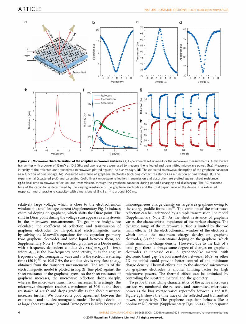
We measured the microwave reflection and transmission fromour device at a frequency of 10.5 GHz (wavelength of 2.8 cm). Weused a TE-polarized microwave transmitter with a power of15 mW and two receivers (Fig. 2a). We applied an externalvoltage bias and measured the variation of the reflected (Fig. 2b)and transmitted (Fig. 2c) microwave power. At a bias voltage of0 V, only 1.8% of the incident beam is reflected from the device.This small reflection is due to the residual charges and/orunintentional doping on the graphene electrodes. The PVCsubstrate and the ionic liquid have negligible microwavereflection (o0.1%, Supplementary Table 1). As we increase thebias voltage, the reflection increases up to 20% at a bias voltage of3.5 V. As the charge density on the capacitor increases, thetransmitted power decreases from 76 to 36% because of enhancedreflection and absorption. The extracted microwave absorptiondue to Joule heating (A¼ 1�T�R where T and R refertransmitted and reflected power) is given in Fig. 2d. Themicrowave absorption of the graphene capacitor can be tunedbetween 21 and 45% of the incoming microwaves for the biasvoltage range of 0–3.5 V. We observed a slight asymmetry inmodulation of microwaves at positive and negative voltages likelydue to different ionic strength of anions and cations of theelectrolyte. The sheet resistance of the graphene electrodes is apractical parameter to understand the microwave response of thisdevice. Figure 2e shows the variation of the total resistance of thedevice as a function of bias voltage. The total resistance (RTþRB,T and B represents the top and bottom electrodes) reaches thepeak value of 8 ko at the charge neutral point (� 0.1 V) anddecreases down to 2.7 kO at a bias voltage of 3.5 V. Afterextracting the contact resistance (RcB0.8 kO, SupplementaryFig. 4), we plot the measured values of the reflection, transmissionand absorption of microwaves at 10.5 GHz frequency, against thesheet resistance of the graphene electrode (Fig. 2f). We alsoobserved small hysteresis when we switched the scan direction(Supplementary Figs 5 and 6). There are two mechanisms thatcause the observed hysteresis in our devices. The first mechanismis the formation of electrical double layers and slow response ofthe electrolyte due to low mobility of the ions in the electrolyte.Hysteresis during charging and discharging is a commonphenomenon in supercapacitors. The second mechanism is theelectrochemical doping of graphene electrodes. When we apply
relatively large voltage, which is close to the electrochemicalwindow, the small leakage current (Supplementary Fig. 7) induceschemical doping on graphene, which shifts the Dirac point. Theshift in Dirac point during the voltage scan appears as a hysteresisin the microwave measurements. To get more insight, wecalculated the coefficient of reflection and transmission ofgraphene electrodes for TE-polarized electromagnetic wavesby solving the Maxwell’s equations for the capacitor geometry(two graphene electrodes and ionic liquid between them, seeSupplementary Note 1). We modelled graphene as a Drude metalwith a frequency dependent conductivity s(o)¼ sDC/(1� iot),where sDC is the low-frequency conductivity, o is the angularfrequency of electromagnetic wave and t is the electron scatteringtime (150 fs)55. At 10.5 GHz, the conductivity is very close to sDC
obtained from the transport measurements. The results of theelectromagnetic model is plotted in Fig. 2f (line plot) against thesheet resistance of the graphene layers. As the sheet resistance ofgraphene increases, the microwave reflection drops sharply,whereas the microwave transmission increases. Interestingly, themicrowave absorption reaches a maximum of 50% at the sheetresistance of 430O and drops gradually as the sheet resistanceincreases further. We observed a good agreement between theexperiment and the electromagnetic model. The slight deviationat large sheet resistance (around Dirac point) is likely because of
inhomogeneous charge density on large-area graphene owing tothe charge puddle formation56. The variation of the microwavereflection can be understood by a simple transmission line model(Supplementary Note 2). As the sheet resistance of graphenevaries, the characteristic impedance of the surface changes. Thedynamic range of the microwave surface is limited by the twomain effects: (1) the electrochemical window of the electrolyte,which limits the maximum charge density on grapheneelectrodes, (2) the unintentional doping on the graphene, whichlimits minimum charge density. However, due to the lack of aband gap, there is always some degree of charges on grapheneelectrodes at unbiased case. A graphene-like material withelectronic band gap (carbon nanotube networks, MoS2 or other2D materials) could provide better control of the minimumcharge density. Thermal effects due to the absorbed microwaveson graphene electrodes is another limiting factor for highmicrowave powers. The thermal effects can be optimized bycontrolling the substrate material and the geometry.
To probe the switching characteristics of the active microwavesurface, we monitored the reflected and transmitted microwavepower as the bias voltage varies repeatedly between 3 and 0 V.Figure 2g,h shows the time trace of the reflected and transmittedpower, respectively. The graphene capacitor behaves like anonlinear RC circuit (Supplementary Figs 12–14). The response
5
10
0 30 60 90 120
45
50
55
60
65
Ref
lect
ion
(%)
Tra
nsm
issi
on (
%)
Time (s)
–3 –2 –1 0 1 2 30
5
10
15
20
Ref
lect
ion
(%)
Voltage (V)
–3 –2 –1 0 1 2 320
25
30
35
40
45
Abs
orpt
ion
(%)
Voltage (V)
0 1 2 3 40
20
40
60
80
100ReflectionTransmission
Absorption
Inte
nsity
(%
)
–4 –2 0 2 42
3
4
5
6
7
8
Res
ista
nce
(kΩ
)
Voltage (V)
V
–3 –2 –1 0 1 2 330
35
40
45
50
55
60
65
70
Tra
nsm
issi
on (
%)
Voltage (V)
Graphene
Ref
lect
ed
Incident
Electrolyte
Transmitted
Rs (kΩ/sq)
Figure 2 | Microwave characterization of the adaptive microwave surfaces. (a) Experimental set-up used for the microwave measurements. A microwave
transmitter with a power of 15 mW at 10.5 GHz and two receivers were used to measure the reflected and transmitted microwave power. (b,c) Measured
intensity of the reflected and transmitted microwaves plotted against the bias voltage. (d) The extracted microwave absorption of the graphene capacitor
as a function of bias voltage. (e) Measured resistance of graphene electrodes (including contact resistance) as a function of bias voltage. (f) The
experimental (scattered plot) and calculated (solid lines) microwave reflection, transmission and absorption are plotted against sheet resistance.
(g,h) Real-time microwave reflection, and transmission, through the graphene capacitor during periodic charging and discharging. The RC response
time of the capacitor is determined by the varying resistance of the graphene electrodes and the total capacitance of the device. The extracted
response time of graphene capacitor with dimensions of 8�8 cm2 is around 300 ms.
time of the device is characterized by the resistance of grapheneelectrodes and the capacitance of the device. We extracted theresponse time of 300 ms for a device with dimensions of8� 8 cm2. This number agrees well with averaged time constantt¼RC¼ 330 ms calculated from the average capacitance(B100 mF) and resistance (B3.3 kO sq� 1) obtained from thetransport measurements. The time constant of the device can bereduced by increasing the charge mobility of graphene electrodes(that is, increasing the grain size of graphene flakes) or ionicmobility of the electrolyte. Using an electrolyte with high ionicconductivity can improve the response time; however, there is atrade of between the ionic mobility and electrochemical stability.
The ionic liquid electrolyte [deme][Tf2N] provides the optimumperformance (see Supplementary Table 1)57.
Switchable radar-absorbing surfaces. After studying the micro-wave response of the graphene capacitors, we would like todemonstrate electrically switchable radar-absorbing surfaces. Themaximum microwave absorption of single-layer graphene islimited to 50% defined by the Maxwell’s equations42,53. To reducethe microwave reflection from the surface, we demonstrated aresonant device architecture (Fig. 3a) that includes the graphenecapacitor and a flat metallic surface, placed at a distance of
0 10 20 30 400
20
40
60
80
100
Mod
ulat
ion
dept
h (%
)
Distance (mm)
0 50 100 150 200
–50
–40
–30
–20
–10
0
Ref
lect
ion
(dB
)
Time (s)
–3 –2 –1 0 1 2 30
20
40
60
Ref
lect
ion
(%)
Voltage (V)
–50
–40
–30
–20
–10
0
Ref
lect
ion
(dB
)
Aluminiumfoil
Graphenecapacitor
10cm
Spacer Contact metals
Back sideFront side
d
V
Noise floor
Noise floor
–50dB
0dB
–3 –2 –1 0 1 2 3
Voltage (V)
0
10
20
30
40
Dis
tanc
e (m
m)
7 8 9 10 11 12
7 8 9 10 11 12
Ref
lect
ion
(dB
)–20
0
–40
–60
–80
Frequency (GHz)
7mm 6mm 5.5mm
Ref
lect
ion
(dB
)
–20
0
–40
–60
–80
0V
–1.5V
Frequency (GHz)
Reflecte
d
Graphene
Incident
Electrolyte
Metallic surface
Figure 3 | Graphene-based switchable radar-absorbing surfaces. (a) Schematic representation of the resonant device including the graphene capacitor
and metallic surface placed at a distance of quarter-wavelength. (b,c) Photographs of the front and the back side of the fabricated device. (d) The measured
microwave reflection at 10.5 GHz plotted against the bias voltage. The red curve shows the reflection in decibel. (e) Real-time reflection from the device
during periodic charging and discharging. The device yields around 50 dB reflection suppression ratio. (f) Broadband reflection spectrum from the device at
various bias voltages. The noise floor is at � 80 dB. (g) Microwave reflection from the device plotted against the bias voltage and the spacer thickness,
which defines the distance between the graphene electrodes and metallic surface. (h) Variation of the modulation depth of the resonant device with
the spacer thickness. When the graphene is at the antinodes, the modulation is around 100%, whereas at the nodes the modulation is close to zero.
(i) Broadband reflection spectra from the device for three different spacer thickness.
quarter of the wavelength (d ¼ l4 cosðyÞ, where, l is the
wavelength and y is the incidence angle). This configuration isknown as Salisbury screen previously used for enhancingmicrowave absorption of resistive materials5 and graphene atinfrared and terahertz frequencies38,58. Figure 3b,c shows thepictures of the front and back side of the resonant device.Surprisingly, placing a flat metal at a suitable distance yields veryhigh reflection suppression at high doping concentration ongraphene. The variation of the microwave reflection of this deviceis shown in Fig. 3d. At 0 V, the reflection is maximum at 60%(� 3 dB) and as we increase the bias voltage, the reflectiondiminishes entirely (o� 45 dB, Fig. 3d). At 3 V, the Fermi energyand charge density on graphene electrodes are around 0.95 eVand 5.5� 1013 cm2, respectively. The time traces of the reflection(Fig. 3e) shows a remarkable reflection suppression ratio ofaround 50 dB, which is limited by our detector. When the gapbetween the graphene electrodes and the metallic surface is aquarter of the wavelength, the reflection from the metallic surfaceforms a standing wave with the antinodal plane (maximum lateralelectric field), which is on graphene electrode. Therefore, thedistance between the graphene electrodes and the metallic surfacedefines the modulation depth (M ¼ Ron �Roff
Ron, Ron and Roff
represent the reflected power at the on- and off-state).Figure 3h shows the variation of the modulation depth with thedistance. Interestingly, when the distance is half-wavelength
(graphene electrodes are at the nodes of the standing wave), wedo not observe any modulation in the reflectivity, because theelectric field on the graphene is zero (Supplementary Fig. 15).Although the resonance behaviour varies with the incidenceangle, this device yields reasonably large modulation for broadincidence angles (Supplementary Figs 16–18).
Next, we would like to discuss some device strategies to coverlarge area and nonplanar surfaces. As microwave has centimetrescale wavelengths, operating these devices over a large area isessential for realistic applications. For this purpose, we developedpixelated surfaces formed by individually addressable hexagonal-shaped devices (Fig. 4a–c). Similar type of multipixel devices hasbeen demonstrated in THz frequencies43,59–61. The individualdevice (Fig. 4d) consists of a graphene capacitor, a solid spacer(2.5-mm-thick cardboard) and metallic back surface (aluminiumfoil). The microwave reflection from an individual device isshown in Fig. 4e. At 1.5 V, the reflection decreases substantiallywith a suppression ratio of 1,000. Figure 4f shows the microwavereflectivity maps of the individual pixel at various voltages. Thestrong reflection at 0 V diminishes at 1.5 V with slightbackground reflection due to the contact metals. Then weimaged four cells (scan area is limited by our scanner) at differentvoltage configurations. When we applied 0 V to the cells weobserved reflection from all devices. However, the reflectivity ofan individual cell can be suppressed at 3 V. Figure 4g shows
–2 –1 0 1 2
0.2
0.4
0.6
0.8
1.0
Ref
lect
ion
(nor
m.)
Voltage (V)
0V 0.25V 0.5V 1V 2V1.5V
4cm
1
0
Front side
Back side
10cm
0V
0V
0V
0V
+3V
0V
0V
0V
0V
+3V
0V
0V0V
0V
+3V
+3V+3V
+3V
+3V
+3V
4cm
2cm
1
0
Graphene
Electrolyte
Graphene
Spacer
Metal
�/4
Figure 4 | Large-area pixelated radar-absorbing surfaces. (a) Photograph of the pixelated microwave surface consists of 14 individually addressable
hexagonal-shaped cells. (b,c) Photograph of the front and back side of an individual cell. (d) Exploited view of the structure of an individual cell showing
the layers. (e) Microwave reflection of an individual cell at 10.5 GHz. (f) Scanning microwave reflection images of a cell at different bias voltages.
(g) Scanning microwave reflection of four cells with different voltage configurations.
reflectivity maps at different voltage configurations. The variationof the reflection within the single cell is due to the reflection fromthe edges and contact metals. These pixelated surfaces wouldyield various possibilities for active camouflage systems byshaping the reflectivity pattern from the multipixel adaptivesurface.
Furthermore, graphene electrodes on flexible polymer sub-strates allow us to fabricate nonplanar adaptive microwavesurfaces as well. Figure 5a,b shows concave and convex sphericalsurfaces formed by multiple individually addressable hexagon-and pentagon-shaped cells. The reflectivity of individual cell(structure shown in the Fig. 4) provides reflection suppression of1,000 for TE polarization. To test an extreme case, we fabricated acylindrical surface with radius of curvature of 2.6 cm (Fig. 5c).Then we placed a metallic cylinder inside the device andmeasured the reflection from surface at various bias voltages.Figure 5d shows the variation of the microwave reflection fromthe cylindrical surface as a function of voltage. Even for a largecurvature, the microwave reflection is suppressed by 45 dB at 2 V.This modulation is slightly less than the flat resonant surface dueto the curvature of the device. The polar plot in Fig. 5e showsthe angular dependence of the reflectivity (at 0 and 2 V) of thecylinder obtained by rotating the cylinder around its axis. Thepolar plot represents tunable radar cross-section of the metalliccylinder. We anticipate that the ability to cover non-planarobjects with these active microwave materials will enable newpossibilities for microwave cloaking43,47.
DiscussionIn summary, we demonstrated a new class of adaptive microwavesurfaces using large-area graphene capacitors. We show thatgraphene electrodes can operate as a tunable Drude metal atmicrowave frequencies owing to the high-mobility carriers whosedensity can be tuned by electrostatic doping. Interestingly, thissimple device structure yields unprecedented ability to control
electromagnetic waves in a very broad spectrum from microwaveto the visible spectra. Combining this ability with various devicearchitectures, we demonstrated electrically switchable radar-absorbing surfaces with reflection suppression ratio of 50 dBwith operation voltages o5 V. Furthermore, we fabricatedvarious adaptive surfaces including pixelated and nonplanarsurfaces. These electrically switchable radar-absorbing surfacesprovide technological advantages over the passive microwaveabsorbers. Our benchmarking studies (see SupplementaryTables 3 and 4) show that the key attributes of these adaptivemicrowave surfaces are the simplicity of device architecture,broadband operation, the mechanical flexibility and potential forlow material cost. We believe that these adaptive microwavesurfaces will open a new chapter for active camouflage systems,which could find immediate applications in radar technologies.Furthermore, integration of these adaptive surfaces with meta-material could yield tunable adaptive cloaking in microwavefrequencies.
MethodsSynthesis and transfer printing process of graphene. We synthesized large-areagraphene by chemical vapour deposition on ultra-smooth copper foils (0.1 mmsurface roughness) purchased from Mitsui mining and smelting company (LTD,B1-SBS). We used a quartz chamber with a diameter of 8 cm and rolled thegraphene foils on a quartz holder. The growth temperature and duration are1,035 �C and 30 min, respectively. We heated the samples until 1,035 �C under H2
flow to reduce the oxide layer of the copper foils. During the growth the partialpressure of CH4 and H2 gases were 1.5 and 3 Torr and corresponding rate of flowsof 40 and 80 sccm, respectively. After terminating the growth by stopping the flowof methane, we cooled the samples down to room temperature. Then we laminated70-mm-thick PVC sheets on graphene-coated copper foils. Following the lamina-tion, the copper foils were etched in diluted nitric acid solution and dried overnightto reduce the chemical doping of nitric acid on graphene.
Transport measurements. We measured capacitance and resistance of thegraphene capacitors using HP 4284 A precision LCR meter as a function of biasvoltage. We applied an AC signal with amplitude of 100 mV together with variableDC voltage to the device. The serial resistance and capacitance were obtained by
–2 –1 0 1 20
10
20
30
40
50
Voltage (V)
Ref
lect
ion
(%)
–50
–40
–30
–20
–10
0
Ref
lect
ion
(dB
)
5cm 5cm
340
320
280
260
240
220
200 180160
140
120
100
80
60
40
020
300
0V
2V
0dB
–80dB
–60dB
–40dB
–20dB
Figure 5 | Nonplanar adaptive radar-absorbing surfaces. (a,b) Photograph of concave and convex hemispherical surfaces formed by individually
addressable hexagon-and pentagon-shaped adaptive cells. (c) Photograph of the cylindrical-shaped switchable radar-absorbing surface placed around a
metallic cylinder. The diameter of the cylinder is 4.2 cm. (d) Reflection from the cylindrical surface containing a metallic cylinder as a function of bias
voltage. (e) Orientation dependence of the normalized reflection from the surface at 0 and 2 V, respectively. At 2 V the reflectivity is suppressed by 50 dB
for all directions. The variation of the intensity on the off-state is due the variation of the distance between the graphene electrodes and metallic cylinder.
using a serial capacitance and resistance (Rs-Cs) model. The voltage bias wasapplied using a Keithly 2400 Source Measure Unit.
Microwave measurements. We used a 15-mW microwave transmitter (GunDiode Microwave Transmitter WA-9314B) operating at 10.5 GHz frequency. Thereflected and transmitted power is measured using two microwave receivers (GunDiode Microwave Receiver) attached to Agilent 34410A 61/2 Digit Multimeter. Themicrowave reflection spectra were recorded using two broadband standard gainhorn antennas (7–12 GHz) attached to a network analyser (0.1–18 GHz AgilentE5063A).
References1. Feng, Y. B., Qiu, T., Shen, C. Y. & Li, X. Y. Electromagnetic and absorption
2. Pitman, K. C., Lindley, M. W., Simkin, D. & Cooper, J. F. Radar absorbers -better by design. IEEE Proc. F 138, 223–228 (1991).
3. Ford, K. L. & Chambers, B. Smart microwave absorber. Electron. Lett. 36, 50–52(2000).
4. Neelakanta, P. S., Stampalia, A. K. & De Groff, D. An actively-controlledmicrowave reflecting surface with binary-pattern modulation. Microwave J. 46,22–63 (2003).
5. Chambers, B. A smart radar absorber. Smart Mater. Struct. 8, 64–72 (1999).6. Neelakanta, P. S., Abello, J. & Gu, C. L. Microwave reflection at an active
surface imbedded with fast-ion conductors.. IEEE Trans. Microw. Theory Tech.40, 1028–1030 (1992).
7. Haupt, R. L. & Lanagan, M. Reconfigurable antennas. IEEE Antennas Propag.Mag. 55, 49–61 (2013).
8. Pendry, J. B., Schurig, D. & Smith, D. R. Controlling electromagnetic fields.Science 312, 1780–1782 (2006).
9. Mirsaneh, M., Furman, E., Ryan, J. V., Lanagan, M. T. & Pantano, C. G.Frequency dependent electrical measurements of amorphous GeSbSechalcogenide thin films. Appl. Phys. Lett. 96, 112907 (2010).
10. Wright, P. V., Chambers, B., Barnes, A., Lees, K. & Despotakis, A. Progress insmart microwave materials and structures. Smart Mater. Struct. 9, 273–279(2000).
11. Vendik, O. G., Hollmann, E. K., Kozyrev, A. B. & Prudan, A. M. Ferroelectrictuning of planar and bulk microwave devices. J. Superconductivity 12, 325–338(1999).
12. Pozar, D. M. & Sanchez, V. Magnetic Tuning of a Microstrip Antenna on aFerrite Substrate. Electron. Lett. 24, 729–731 (1988).
13. Hansen, R. C. & Burke, M. Antennas with magneto-dielectrics. Microwave Opt.Technol. Lett. 26, 75–78 (2000).
14. Novoselov, K. S. et al. Two-dimensional atomic crystals. Proc. Natl Acad. Sci.USA 102, 10451–10453 (2005).
15. Novoselov, K. S. et al. Two-dimensional gas of massless Dirac fermions ingraphene. Nature 438, 197–200 (2005).
16. Wang, C. et al. The electromagnetic property of chemically reduced grapheneoxide and its application as microwave absorbing material. Appl. Phys. Lett. 98,072906 (2011).
17. Singh, V. K. et al. Microwave absorbing properties of a thermally reducedgraphene oxide/nitrile butadiene rubber composite. Carbon N. Y. 50,2202–2208 (2012).
18. Sun, X. G. Effect of carbon nanotube content on the radar absorbing properties.of carbon nanotube/resin composites. N. Carbon Mater. 22, 375–378 (2007).
19. Zhao, X. C. et al. Excellent microwave absorption property of graphene-coatedFe nanocomposites. Sci. Rep. 3, 3421 (2013).
20. Wu, B. A. et al. Experimental demonstration of a transparent graphenemillimetre wave absorber with 28% fractional bandwidth at 140 GHz. Sci. Rep.4, 4130 (2014).
21. Dragoman, M. et al. Graphene for microwaves. IEEE Microw. Mag. 11, 81–86(2010).
22. Collier, R. J. & Hasko, D. G. Measurement of the sheet resistance of resistivefilms on thin substrates from 120 to 175 GHz using dielectric waveguides.J. Appl. Phys. 91, 2547–2549 (2002).
23. Zheng, Z. W. et al. Microwave and optical saturable absorption in graphene.Opt. Express 20, 23201–23214 (2012).
24. Deligeorgis, G. et al. Microwave propagation in graphene. Appl. Phys. Lett. 95,073107 (2009).
25. Wu, Y. Q. et al. Microwave transmission properties of chemical vapordeposition graphene. Appl. Phys. Lett. 101, 053110 (2012).
26. Chamanara, N., Sounas, D., Szkopek, T. & Caloz, C. Optically transparent andflexible graphene reciprocal and nonreciprocal microwave planar components.IEEE Microwave Wireless Componet Lett. 22, 360–362 (2012).
27. Gogoi, J. P., Bhattacharyya, N. S. & Bhattacharyya, S. Single layer microwaveabsorber based on expanded graphite-novolac phenolic resin composite forX-band applications. Composites Part B 58, 518–523 (2014).
28. Ando, T., Fowler, A. B. & Stern, F. Electronic-Properties of Two-DimensionalSystems. Rev. Mod. Phys. 54, 437–672 (1982).
29. Tagantsev, A. K., Sherman, V. O., Astafiev, K. F., Venkatesh, J. & Setter, N.Ferroelectric materials for microwave tunable applications. J. Electroceramics11, 5–66 (2003).
30. Lee, C. H. et al. Exploiting dimensionality and defect mitigation to createtunable microwave dielectrics. Nature 502, 532–536 (2013).
31. Buckley, L. J. & Mohl, D. Smart Polymeric Materials for Active Camouflage. InActive Materials and Adaptive Structures SPIE Conf. 23–26 (1992).
32. Rose, T. L. et al. A microwave shutter using conductive polymers. Synth. Met.85, 1439–1440 (1997).
33. Freeman, J. L., Lamberty, B. J. & Andrews, G. S. Optoelectronicallyreconfigurable monopole antenna. Electron. Lett. 28, 1502–1503 (1992).
34. Grewal, G. & Hanson, G. W. Optically-controlled solid-state plasma leaky-waveantenna. Microwave Opt. Technol. Lett. 39, 450–453 (2003).
35. Bernhard, J. T., Kiely, E. & Washington, G. A smart mechanically actuated two-layer electromagnetically coupled microstrip antenna with variable frequency,bandwidth, and antenna gain. IEEE Trans. Antenna Propag. 49, 597–601(2001).
36. Washington, G., Yoon, H. S., Angelino, M. & Theunissen, W. H. Design,modeling, and optimization of mechanically reconfigurable aperture antennas.IEEE Trans. Antenna Propag. 50, 628–637 (2002).
37. Lee, S. H. et al. Switching terahertz waves with gate-controlled active graphenemetamaterials. Nat. Mater. 11, 936–941 (2012).
38. Sensale-Rodriguez, B. et al. Extraordinary control of terahertz beamreflectance in graphene electro-absorption modulators. Nano Lett. 12,4518–4522 (2012).
39. Tamagnone, M., Fallahi, A., Mosig, J. R. & Perruisseau-Carrier, J. Fundamentallimits and near-optimal design of graphene modulators and non-reciprocaldevices. Nat. Photon 8, 556–563 (2014).
40. Badhwar, S. et al. Indirect modulation of a terahertz quantum cascade laserusing gate tunable graphene. IEEE Photon. J. 4, 1776–1782 (2012).
41. Sensale-Rodriguez, B. et al. Unique prospects for graphene-based terahertzmodulators. Appl. Phys. Lett. 99, 113104 (2011).
42. Sensale-Rodriguez, B. et al. Broadband graphene terahertz modulators enabledby intraband transitions. Nat. Commun. 3, 780 (2012).
43. Chen, P. Y. et al. Nanostructured graphene metasurface for tunable terahertzcloaking. N. J. Phys. 15, 123029 (2013).
44. Ju, L. et al. Graphene plasmonics for tunable terahertz metamaterials. Nat.Nanotech. 6, 630–634 (2011).
45. Fallahi, A. & Perruisseau-Carrier, J. Design of tunable biperiodic graphenemetasurfaces. Phys. Rev. B 86, 195408 (2012).
46. Gomez-Diaz, J. S. et al. Self-biased reconfigurable graphene stacks for terahertzplasmonics. Preprint at http://arxiv.org/abs/1405.3320 (2014).
47. Chen, P. Y. & Alu, A. Atomically thin surface cloak using graphene monolayers.ACS Nano 5, 5855–5863 (2011).
48. Sensale-Rodriguez, B., Yan, R. S., Liu, L., Jena, D. & Xing, H. G. Graphene forreconfigurable terahertz optoelectronics. Proc. IEEE 101, 1705–1716 (2013).
49. Polat, E. O. & Kocabas, C. Broadband optical modulators based on graphenesupercapacitors. Nano Lett. 13, 5851–5857 (2013).
50. Mak, K. F., Ju, L., Wang, F. & Heinz, T. F. Optical spectroscopy of graphene:from the far infrared to the ultraviolet. Solid State Commun. 152, 1341–1349(2012).
51. Zhang, X. et al. A graphene-based broadband optical modulator. Nature 474,64–67 (2011).
52. Dorgan, V. E., Bae, M. H. & Pop, E. Mobility and saturation velocity ingraphene on SiO2. Appl. Phys. Lett. 97, 082112 (2010).
53. Bosman, H., Lau, Y. Y. & Gilgenbach, R. M. Microwave absorption on a thinfilm. Appl. Phys. Lett. 82, 1353 (2003).
54. Baylam, I. et al. Femtosecond pulse generation with voltage-controlledgraphene saturable absorber. Opt. Lett. 39, 5180–5183 (2014).
55. Brida, D. et al. Ultrafast collinear scattering and carrier multiplication ingraphene. Nat. Commun. 4, 1987 (2013).
56. Adam, S., Hwang, E. H., Galitski, V. M. & Das Sarma, S. A self-consistenttheory for graphene transport. Proc. Natl Acad. Sci. USA 104, 18392–18397(2007).
57. Hayyan, M., Mjalli, F. S., Hashim, M. A., AlNashef, I. M. & Mei, T. X.Investigating the electrochemical windows of ionic liquids. J. Ind. Eng. Chem.19, 106–112 (2013).
58. Woo, J. M., Kim, M. S., Kim, H. W. & Jang, J. H. Graphene based salisburyscreen for terahertz absorber. Appl. Phys. Lett. 104, 081106 (2014).
59. Sensale-Rodriguez, B. et al. Terahertz imaging employing graphene modulatorarrays. Opt. Express 21, 2324–2330 (2013).
60. Watts, C. M. et al. Terahertz compressive imaging with metamaterial spatiallight modulators. Nat. Photon 8, 605–609 (2014).
61. Carrasco, E., Tamagnone, M. & Perruisseau-Carrier, J. Tunable graphenereflective cells for THz reflectarrays and generalized law of reflection. Appl.Phys. Lett. 102, 104103 (2013).
AcknowledgementsThis work was supported by the Scientific and Technological Research Council of Turkey(TUBITAK) grant no. 114F052 and 113F278.
Author contributionsC.K. and O.B. proposed the idea, O.B. and C.K. planned the experiment; O.B. fabricatedthe samples. C.K. and O.B. performed the experiments, analysed the data and wrote themanuscript. E.O.P and N.K. helped for the synthesis of graphene and microwavemeasurements. All authors discussed the results and contributed to the scientificinterpretation as well as to the writing of the manuscript.
Additional informationSupplementary Information accompanies this paper at http://www.nature.com/naturecommunications
Competing financial interests: The authors declare no competing financial interests.
Reprints and permission information is available online at http://npg.nature.com/reprintsandpermissions/
How to cite this article: Balci, O. et al. Graphene-enabled electrically switchable radarabsorbing surfaces. Nat. Commun. 6:6628 doi: 10.1038/ncomms7628 (2015).