1 Graphene-MoS2 Hybrid Technology for Large-Scale Two- Dimensional Electronics Lili Yu 1* , Yi-Hsien Lee 2 , Xi Ling 1 , Elton J.G. Santos 3, , Yong Cheol Shin 4 , Yuxuan Lin 1 , Madan Dubey 5 , Efthimios Kaxiras 3,6 , Jing Kong 1 , Han Wang 1* , and Tomás Palacios 1* 1 Department of Electrical Engineering and Computer Science, Massachusetts Institute of Technology, 77 Massachusetts Avenue, Cambridge, MA 02139, USA. 2 Materials Science and Engineering, National Tsing-Hua University, Hsinchu, 30013, Taiwan 3 School of Engineering and Applied Sciences, Harvard University, Cambridge, MA 02138, USA 4 Department of Materials Science and Engineering, Massachusetts Institute of Technology, 77 Massachusetts Avenue, Cambridge, MA 02139, USA. 5 United States Army Research Laboratory, 2800 Powder Mill Road, Adelphi, Maryland 20783-1197, United States 6 Department of Physics, Harvard University, Cambridge, MA 02138, USA Present address: Department of Chemical Engineering, Stanford University, Stanford, California 94305, United States, SLAC National Accelerator Laboratory, SUNCAT Center for Interface Science and Catalysis, Menlo Park, California 94025, United States Corresponding author E-mail: [email protected], [email protected], [email protected]Abstract Two-dimensional (2D) materials have generated great interest in the last few years as a new toolbox for electronics. This family of materials includes, among others, metallic graphene, semiconducting transition metal dichalcogenides (such as MoS2) and insulating Boron Nitride. These materials and their heterostructures offer excellent mechanical flexibility, optical transparency and favorable transport properties for realizing electronic, sensing and optical systems on arbitrary surfaces. In this paper, we demonstrate a novel technology for constructing large-scale electronic systems based on graphene/molybdenum disulfide (MoS2) heterostructures grown by chemical vapor deposition. We have fabricated high-performance devices and circuits based on this heterostructure, where MoS2 is used as the transistor channel and graphene as contact electrodes and circuit interconnects. We provide a systematic comparison of the graphene/MoS2 heterojunction contact to more traditional MoS2-metal junctions, as well as a theoretical investigation, using density functional theory, of the origin of the Schottky barrier height. The tunability of the graphene work function with electrostatic doping significantly improves the ohmic contact to MoS2. These high-performance large-scale devices and circuits based on this 2D heterostructure pave the way for practical flexible transparent electronics. A
Transcript
1
Graphene-MoS2 Hybrid Technology for Large-Scale Two-
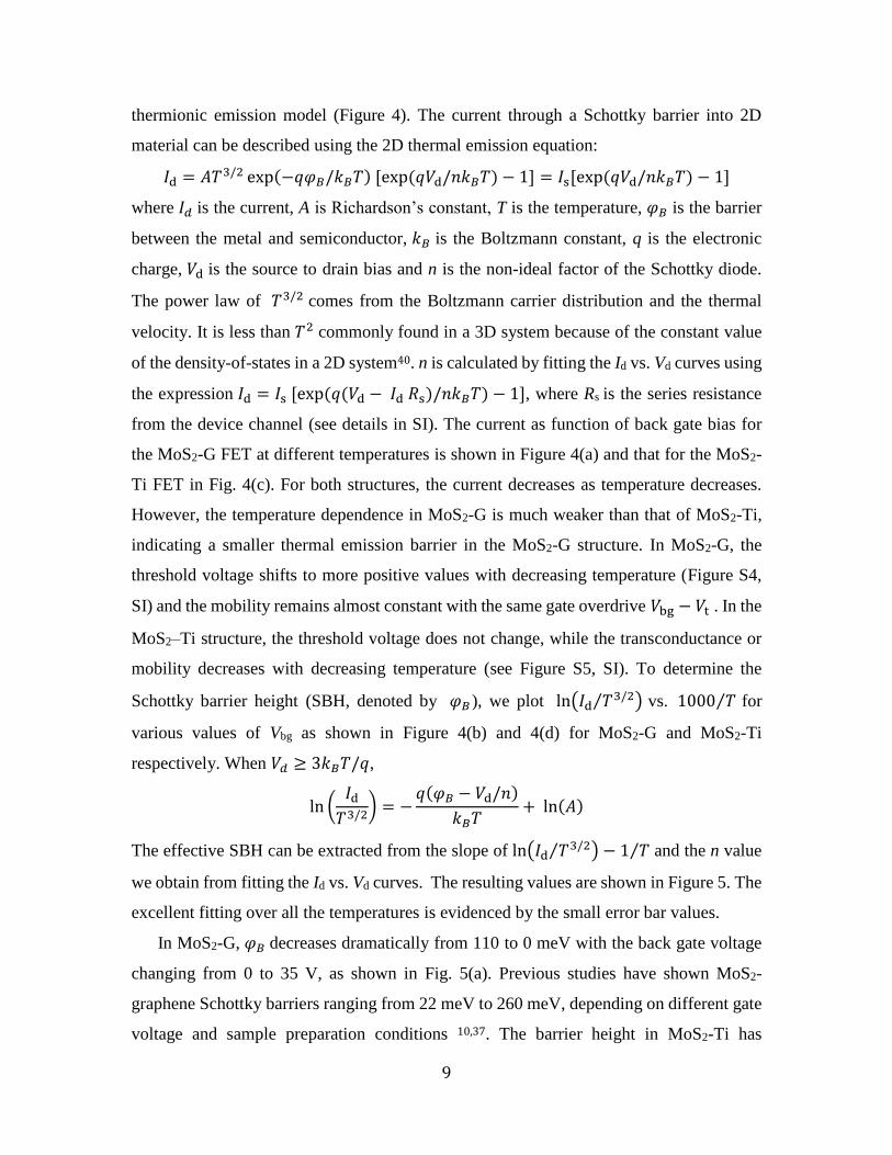
where 𝐼𝑑 is the current, A is Richardson’s constant, T is the temperature, 𝜑𝐵 is the barrier
between the metal and semiconductor, 𝑘𝐵 is the Boltzmann constant, q is the electronic
charge, 𝑉d is the source to drain bias and n is the non-ideal factor of the Schottky diode.
The power law of 𝑇3/2 comes from the Boltzmann carrier distribution and the thermal
velocity. It is less than 𝑇2 commonly found in a 3D system because of the constant value
of the density-of-states in a 2D system40. n is calculated by fitting the Id vs. Vd curves using
the expression 𝐼d = 𝐼s [exp (𝑞(𝑉d − 𝐼d 𝑅s)/𝑛𝑘𝐵𝑇) − 1], where Rs is the series resistance
from the device channel (see details in SI). The current as function of back gate bias for
the MoS2-G FET at different temperatures is shown in Figure 4(a) and that for the MoS2-
Ti FET in Fig. 4(c). For both structures, the current decreases as temperature decreases.
However, the temperature dependence in MoS2-G is much weaker than that of MoS2-Ti,
indicating a smaller thermal emission barrier in the MoS2-G structure. In MoS2-G, the
threshold voltage shifts to more positive values with decreasing temperature (Figure S4,
SI) and the mobility remains almost constant with the same gate overdrive 𝑉bg − 𝑉t . In the
MoS2–Ti structure, the threshold voltage does not change, while the transconductance or
mobility decreases with decreasing temperature (see Figure S5, SI). To determine the
Schottky barrier height (SBH, denoted by 𝜑𝐵 ), we plot ln(𝐼d 𝑇3/2⁄ ) vs. 1000 𝑇⁄ for
various values of Vbg as shown in Figure 4(b) and 4(d) for MoS2-G and MoS2-Ti
respectively. When 𝑉𝑑 ≥ 3𝑘𝐵𝑇/𝑞,
ln (𝐼d
𝑇3/2) = −
𝑞(𝜑𝐵 − 𝑉d/𝑛)
𝑘𝐵𝑇+ ln(𝐴)
The effective SBH can be extracted from the slope of ln(𝐼d 𝑇3/2⁄ ) − 1 𝑇⁄ and the n value
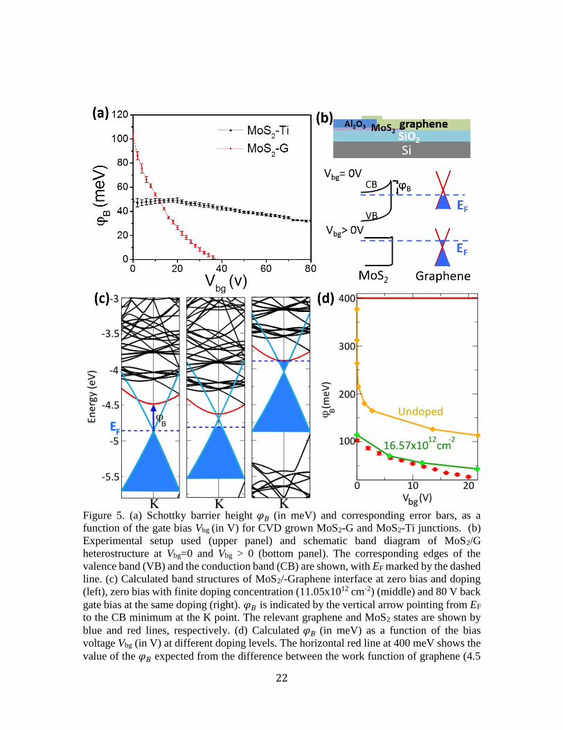
we obtain from fitting the Id vs. Vd curves. The resulting values are shown in Figure 5. The
excellent fitting over all the temperatures is evidenced by the small error bar values.
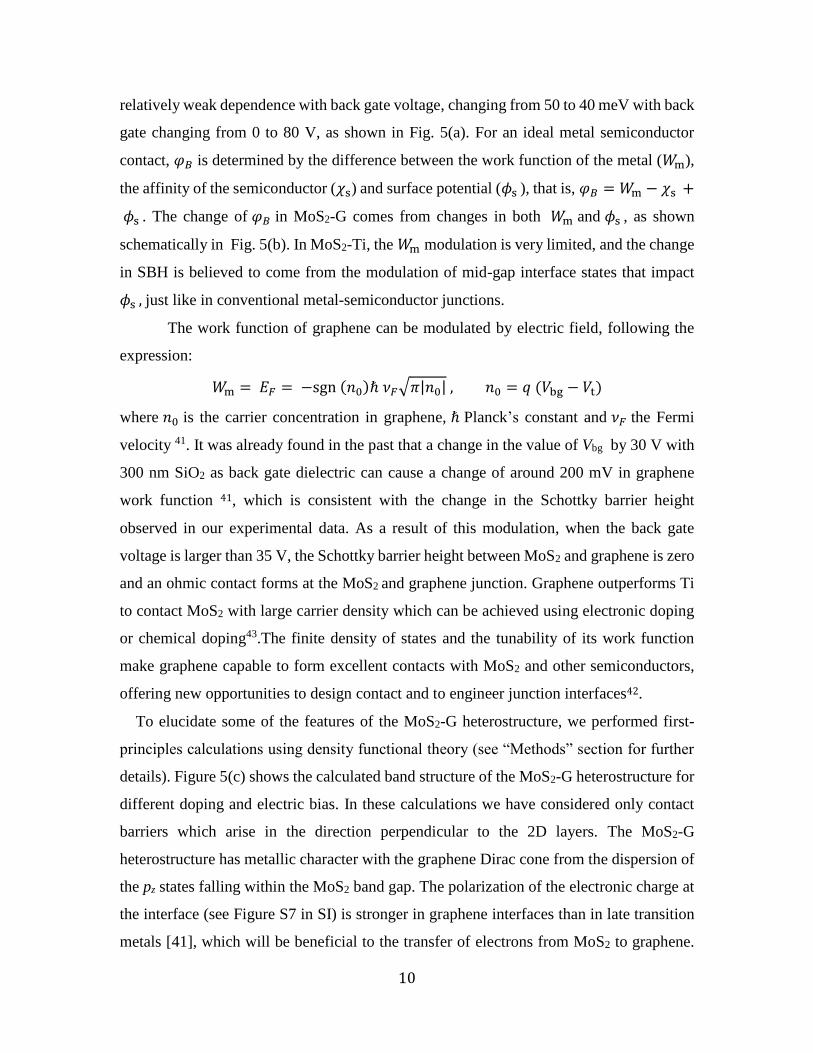
In MoS2-G, 𝜑𝐵 decreases dramatically from 110 to 0 meV with the back gate voltage
changing from 0 to 35 V, as shown in Fig. 5(a). Previous studies have shown MoS2-
graphene Schottky barriers ranging from 22 meV to 260 meV, depending on different gate
voltage and sample preparation conditions 10,37. The barrier height in MoS2-Ti has
10
relatively weak dependence with back gate voltage, changing from 50 to 40 meV with back
gate changing from 0 to 80 V, as shown in Fig. 5(a). For an ideal metal semiconductor
contact, 𝜑𝐵 is determined by the difference between the work function of the metal (𝑊m),
the affinity of the semiconductor (𝜒s) and surface potential (𝜙s ), that is, 𝜑𝐵 = 𝑊m − 𝜒s +
𝜙s . The change of 𝜑𝐵 in MoS2-G comes from changes in both 𝑊m and 𝜙s , as shown
schematically in Fig. 5(b). In MoS2-Ti, the 𝑊m modulation is very limited, and the change
in SBH is believed to come from the modulation of mid-gap interface states that impact
𝜙s , just like in conventional metal-semiconductor junctions.
The work function of graphene can be modulated by electric field, following the
expression:
𝑊m = 𝐸𝐹 = −sgn (𝑛0)ℏ 𝜈𝐹√𝜋|𝑛0| , 𝑛0 = 𝑞 (𝑉bg − 𝑉t)
where 𝑛0 is the carrier concentration in graphene, ℏ Planck’s constant and 𝜈𝐹 the Fermi
velocity 41. It was already found in the past that a change in the value of Vbg by 30 V with
300 nm SiO2 as back gate dielectric can cause a change of around 200 mV in graphene
work function 41, which is consistent with the change in the Schottky barrier height
observed in our experimental data. As a result of this modulation, when the back gate
voltage is larger than 35 V, the Schottky barrier height between MoS2 and graphene is zero
and an ohmic contact forms at the MoS2 and graphene junction. Graphene outperforms Ti
to contact MoS2 with large carrier density which can be achieved using electronic doping
or chemical doping43.The finite density of states and the tunability of its work function
make graphene capable to form excellent contacts with MoS2 and other semiconductors,
offering new opportunities to design contact and to engineer junction interfaces42.
To elucidate some of the features of the MoS2-G heterostructure, we performed first-
principles calculations using density functional theory (see “Methods” section for further
details). Figure 5(c) shows the calculated band structure of the MoS2-G heterostructure for
different doping and electric bias. In these calculations we have considered only contact
barriers which arise in the direction perpendicular to the 2D layers. The MoS2-G
heterostructure has metallic character with the graphene Dirac cone from the dispersion of
the pz states falling within the MoS2 band gap. The polarization of the electronic charge at
the interface (see Figure S7 in SI) is stronger in graphene interfaces than in late transition
metals [41], which will be beneficial to the transfer of electrons from MoS2 to graphene.
11
Because of the very small density of states near the Fermi level (around the graphene Dirac
point), the behavior of the device is sensitive to the position of 𝐸𝐹 inside of the band gap,
which can be changed by electronic doping or external electric fields. At conditions of zero
external bias and no doping (left panel in Fig.5(c)), 𝐸𝐹 is at the Dirac point, and
corresponds to small charge transfer (~0.01 electrons per cell from MoS2 to graphene) and
relatively weak interactions (~55 meV per C atom). At finite doping (middle panel in Fig.
5(c)) or electric fields (right panel in Fig. 5(c)), 𝐸𝐹 is shifted away from the Dirac point,
which changes the magnitude of the Schottky barrier height 𝜑𝐵. In this case, the barrier is
given by the difference between the Fermi level of the combined system and the conduction
band minimum of MoS2 at the K point in the Brillouin zone. The results of barrier height
change as a function of the external bias are shown in Fig. 5(d): At no doping and zero
electric bias, the barrier height is 385 meV, close to the value of 400 meV obtained by
simply calculating the difference between the graphene work function and the electron
affinity of MoS2. In the real system, a small amount of doping will shift the value of 𝜑𝐵
significantly from this value. When an external electric field is applied, 𝜑𝐵 decreases
monotonically with increasing values of the bias. The amount by which 𝜑𝐵 changes
depends on the level of doping. The strong dependence of the value of 𝜑𝐵 on the gate
voltage, in the range 0< Vbg< 2 V is due to the very low density of states near the graphene
Dirac point, as mentioned above, which results in large shift of the Fermi level for small
amount of induced charge. For values of Vbg> 6 V, the change in 𝜑𝐵 is smaller, and its
slope is almost independent of the doping level at high concentrations (~1013 cm-2, see
Figure S8 in SI for different values of doping).
In summary, a novel 2D electronic system using heterostructures of single-layer MoS2
and graphene has been demonstrated where MoS2 serves as the channel material and
graphene is used as both the ohmic and gate contacts, and the interconnects for the 2D
electronic system. This technology represents the first large-scale platform for constructing
electronics based on Van der Waals heterostructures of 2D material monolayers. Both
MoS2 and graphene monolayers were grown using low-cost CVD methods, which are
easily scalable to any size on arbitrary substrates. This work lays the foundation for a
scalable all-2D-material electronics platform capable of taking full advantage of the
mechanical flexibility and electrostatic integrity offered by monolayer electronic materials
12
for applications in flexible and transparent electronics. Our systematic analysis of using
graphene as contact material to interface with 2D semiconductors (in this study MoS2) for
effective carrier injection into the channel, demonstrates that the tunable Fermi level offers
unprecedented flexibility for matching the work-function of the contacts with the channel.
Combining the many advantages of graphene in high frequency electronics44–46, and its
potential use as a new interconnect material superior to metals42,47 at the nanometer scale48,
the technological framework demonstrated in this work opens the door to many new
opportunities for designing novel electronic systems.
Methods
Low-T ALD: The low-temperature ALD deposition of Al2O3 was performed on a
commercial Savannah ALD system from Cambridge NanoTech at 100 C using alternating
cycles of H2O and trimethylaluminum (TMA) as the precursors. The purge time between
each cycle is 60 s to allow the full reaction.
AFM and Raman spectroscopy: Atomic force microscopy (AFM) for identifying the thin
film thickness was performed on a Veeco DimensionTM 3100 system. Raman spectroscopy
was performed with a 532 nm Nd:YAG laser. All optical micrographs were taken with a
Zeiss Axio Imager.A1m microscope.
Device and circuit characterization: Device characterization was performed using an
Agilent 4155C semiconductor parameter analyzer and a Lakeshore cryogenic probe station
with micromanipulation probes. All measurements were done in vacuum (3 × 10⁻⁶ Torr)
at room temperature.
First-principles electronic structure calculations: The calculations reported here are
based on density functional theory calculations using the SIESTA code 49. The generalized
gradient approximation 50 and nonlocal van der Waals density functional 51 was used
together with double- plus polarized basis set, and norm-conserving Troullier-Martins
pseudopotentials 52 to represent the atomic cores. The resolution of the real-space grid used
to calculate the Hartree and exchange-correlation contribution to the total energy was
chosen to be equivalent to 150 Ry plane-wave cut-off. Atomic coordinates were allowed
to relax using a conjugate-gradient algorithm until all forces were smaller in magnitude
than 0.01 eV/Å. To simulate the interface between graphene and MoS2 layers, supercells
13
containing up to 488 atoms were constructed using a graphene supercell of 5 × 5 and a
MoS2 supercell of 4 × 4, which are approximately lattice matched, in different stacking
configurations. To avoid interactions between layer images the distance between periodic
images of the structures along the direction perpendicular to the surface was always larger
than 20 Å. The number of k-points was chosen according to the Monkhorst-Pack 53 scheme,
and was set to the equivalent of a 47 × 47 × 1 grid in the primitive unit cell of graphene,
which gives well-converged values for all the calculated properties. We used a Fermi-Dirac
distribution with an electronic temperature of 𝑘𝐵𝑇 = 21 meV. The external electric field
is introduced through a saw-tooth-like electrostatic potential in the direction perpendicular
to the MoS2-G plane. The different doping levels are obtained by adding a certain amount
of electrons to the system and imposing a compensating uniform background in order to
converge the total energy and the long-range Coulomb interactions 54[52].
Acknowledgement The authors would like to thank Allen Hsu and Xu Zhang for their
helpful advice on device fabrication and measurement. The authors acknowledge financial
support from the Office of Naval Research (ONR) PECASE Program, the ONR GATE
MURI program, the Army Research Laboratory, and Center for Integrated Quantum
Materials (CIQM). This research has made use of the MIT’s Microsystem Technology
Laboratory cleanrooms. We acknowledge the use of computational resources provided by
the Extreme Science and Engineering Discovery Environment (XSEDE), supported by
NSF grants number TG-DMR120049 and TG-PHY120021.
Additional information
The authors declare no competing financial interests.
Supporting information
CVD growth of MoS2 and single layer graphene, Alignment accuracy of fabrication process, Top gate performances of MoS2-G FET, Temperature dependence of MoS2–
Ti and MoS2–G FETs, calculation of n and Rs, density functional theory (DFT) calculation of graphene-MoS2 interface. This material is available free of charge via the Internet at http://pubs.acs.org.
1. Radisavljevic, B., Radenovic, A., Brivio, J., Giacometti, V. & Kis, A. Single-layer MoS2 transistors. Nature Nanotechnology 6, 147–150 (2011).
2. Liu, H. & Ye, P. D. Dual-Gate MOSFET With Atomic-Layer-Deposited as Top-Gate Dielectric. IEEE Electron Device Letters 33, 546–548 (2012).
3. Liu, H., Neal, A. T. & Ye, P. D. Channel Length Scaling of MoS2 MOSFETs. ACS Nano 6, 8563–8569 (2012).
4. Das, S., Chen, H.-Y., Penumatcha, A. V. & Appenzeller, J. High Performance Multilayer MoS2 Transistors with Scandium Contacts. Nano Lett. 13, 100–105 (2013).
5. Fang, H. et al. Degenerate n-Doping of Few-Layer Transition Metal Dichalcogenides by Potassium. Nano Lett. 13, 1991–1995 (2013).
6. Forrest, S. R. The path to ubiquitous and low-cost organic electronic appliances on plastic. Nature 428, 911–918 (2004).
7. Dimitrakopoulos, C. D. & Mascaro, D. J. Organic thin-film transistors: A review of recent advances. IBM Journal of Research and Development 45, 11–27 (2001).
8. Kim, D.-H. et al. Complementary Logic Gates and Ring Oscillators on Plastic Substrates by Use of Printed Ribbons of Single-Crystalline Silicon. IEEE Electron Device Letters 29, 73–76 (2008).
9. Lee, G.-H. et al. Flexible and Transparent MoS2 Field-Effect Transistors on Hexagonal Boron Nitride-Graphene Heterostructures. ACS Nano (2013). doi:10.1021/nn402954e
10. Yoon, J. et al. Highly Flexible and Transparent Multilayer MoS2 Transistors with Graphene Electrodes. Small n/a–n/a (2013). doi:10.1002/smll.201300134
11. Georgiou, T. et al. Vertical field-effect transistor based on graphene-WS2 heterostructures for flexible and transparent electronics. Nat Nano 8, 100–103 (2013).
12. Wang, H., Hsu, A., Wu, J., Kong, J. & Palacios, T. Graphene-Based Ambipolar RF Mixers. IEEE Electron Device Letters 31, 906 –908 (2010).
13. Lee, Y. et al. Wafer-Scale Synthesis and Transfer of Graphene Films. Nano Lett. 10, 490–493 (2010).
14. Wang, H. et al. Integrated Circuits Based on Bilayer MoS2 Transistors. Nano Lett. 12, 4674–4680 (2012).
15. Wang, H. et al. Large-scale 2D electronics based on single-layer MoS2 grown by chemical vapor deposition. in Electron Devices Meeting (IEDM), 2012 IEEE International 4.6.1–4.6.4 (2012). doi:10.1109/IEDM.2012.6478980
16. Bertolazzi, S., Krasnozhon, D. & Kis, A. Nonvolatile Memory Cells Based on MoS2/Graphene Heterostructures. ACS Nano 7, 3246–3252 (2013).
17. Lee, Y.-H. et al. Synthesis of Large-Area MoS2 Atomic Layers with Chemical Vapor Deposition. Advanced Materials 24, 2320–2325 (2012).
18. Lee, Y.-H. et al. Synthesis and Transfer of Single-Layer Transition Metal Disulfides on Diverse Surfaces. Nano Lett. 13, 1852–1857 (2013).
19. Mak, K., Lee, C., Hone, J., Shan, J. & Heinz, T. Atomically Thin MoS_2: A New Direct-Gap Semiconductor. Physical Review Letters 105, (2010).
15
20. Splendiani, A. et al. Emerging photoluminescence in monolayer MoS2. Nano letters 10, 1271–1275 (2010).
21. Ramasubramaniam, A. Large excitonic effects in monolayers of molybdenum and tungsten dichalcogenides. Phys. Rev. B 86, 115409 (2012).
22. Berkelbach, T. C., Hybertsen, M. S. & Reichman, D. R. Theory of neutral and charged excitons in monolayer transition metal dichalcogenides. Phys. Rev. B 88, 045318 (2013).
23. Berghäuser, G. & Malic, E. Analytical approach to excitonic properties of MoS2. Phys. Rev. B 89, 125309 (2014).
24. Lee, C. et al. Anomalous Lattice Vibrations of Single- and Few-Layer MoS2. ACS Nano 4, 2695–2700 (2010).
25. Kuo, S.-W., Kao, H.-C. & Chang, F.-C. Thermal behavior and specific interaction in high glass transition temperature PMMA copolymer. Polymer 44, 6873–6882 (2003).
26. Li, X. et al. Large-Area Synthesis of High-Quality and Uniform Graphene Films on Copper Foils. Science 324, 1312–1314 (2009).
27. Bhaviripudi, S., Jia, X., Dresselhaus, M. S. & Kong, J. Role of Kinetic Factors in Chemical Vapor Deposition Synthesis of Uniform Large Area Graphene Using Copper Catalyst. Nano Lett. 10, 4128–4133 (2010).
28. Reina, A. et al. Large Area, Few-Layer Graphene Films on Arbitrary Substrates by Chemical Vapor Deposition. Nano Lett. 9, 30–35 (2009).
29. Kim, K. S. et al. Large-scale pattern growth of graphene films for stretchable transparent electrodes. Nature 457, 706–710 (2009).
30. Kim, S. et al. High-mobility and low-power thin-film transistors based on multilayer MoS2 crystals. Nat Commun 3, 1011 (2012).
31. Kang, J., Sarkar, D., Liu, W., Jena, D. & Banerjee, K. A computational study of metal-contacts to beyond-graphene 2D semiconductor materials. in Electron Devices Meeting (IEDM), 2012 IEEE International 17.4.1–17.4.4 (2012). doi:10.1109/IEDM.2012.6479060
32. Popov, I., Seifert, G. & Tománek, D. Designing Electrical Contacts to MoS_2 Monolayers: A Computational Study. Phys. Rev. Lett. 108, 156802 (2012).
33. Fuhrer, M. S. & Hone, J. Measurement of mobility in dual-gated MoS2 transistors. Nat Nano 8, 146–147 (2013).
34. Dean, C. R. et al. Boron nitride substrates for high-quality graphene electronics. Nat Nano 5, 722–726 (2010).
35. Liu, H. et al. Statistical Study of Deep Submicron Dual-Gated Field-Effect Transistors on Monolayer Chemical Vapor Deposition Molybdenum Disulfide Films. Nano Lett. (2013). doi:10.1021/nl400778q
36. Kim, B.-J., Shin, H.-A.-S., Choi, I.-S. & Joo, Y.-C. Electrical failure and damage analysis of multi-layer metal films on flexible substrate during cyclic bending deformation. in Physical and Failure Analysis of Integrated Circuits (IPFA), 2011 18th IEEE International Symposium on the 1–4 (2011). doi:10.1109/IPFA.2011.5992725
37. Yu, W. J. et al. Vertically stacked multi-heterostructures of layered materials for logic transistors and complementary inverters. Nat Mater 12, 246–252 (2013).
16
38. Pu, J. et al. Highly Flexible MoS2 Thin-Film Transistors with Ion Gel Dielectrics. Nano Lett. 12, 4013–4017 (2012).
39. Chang, H.-Y. et al. High-Performance, Highly Bendable MoS2 Transistors with High-K Dielectrics for Flexible Low-Power Systems. ACS Nano 7, 5446–5452 (2013).
40. Chen, J.-R. et al. Control of Schottky Barriers in Single Layer MoS2 Transistors with Ferromagnetic Contacts. Nano Lett. 13, 3106–3110 (2013).
41. Yu, Y.-J. et al. Tuning the Graphene Work Function by Electric Field Effect. Nano Lett. 9, 3430–3434 (2009).
42. Byun, K.-E. et al. Graphene for True Ohmic Contact at Metal–Semiconductor Junctions. Nano Lett. 13, 4001–4005 (2013).
43. Shi, Y. et al. Work Function Engineering of Graphene Electrode via Chemical Doping. ACS Nano 4, 2689–2694 (2010).
44. Han Wang, Nezich, D., Jing Kong & Palacios, T. Graphene Frequency Multipliers. IEEE Electron Device Letters 30, 547–549 (2009).
45. Wang, H. et al. BN/Graphene/BN transistors for RF applications. Electron Device Letters, IEEE 32, 1209–1211 (2011).
46. Palacios, T., Hsu, A. & Wang, H. Applications of graphene devices in RF communications. IEEE Communications Magazine 48, 122–128 (2010).
47. Chen, X. et al. Fully Integrated Graphene and Carbon Nanotube Interconnects for Gigahertz High-Speed CMOS Electronics. IEEE Transactions on Electron Devices 57, 3137–3143 (2010).
48. Naeemi, A. & Meindl, J. D. Performance Benchmarking for Graphene Nanoribbon, Carbon Nanotube, and Cu Interconnects. in Interconnect Technology Conference, 2008. IITC 2008. International 183–185 (2008). doi:10.1109/IITC.2008.4546961
49. Soler, J. M. et al. The SIESTA method for ab initio order-N materials simulation. J. Phys.: Condens. Matter 14, 2745 (2002).
50. Perdew, J. P., Burke, K. & Ernzerhof, M. Generalized Gradient Approximation Made Simple. Phys. Rev. Lett. 77, 3865–3868 (1996).
51. Dion, M., Rydberg, H., Schröder, E., Langreth, D. C. & Lundqvist, B. I. Van der Waals Density Functional for General Geometries. Phys. Rev. Lett. 92, 246401 (2004).
52. Troullier, N. & Martins, J. L. Efficient pseudopotentials for plane-wave calculations. Phys. Rev. B 43, 1993–2006 (1991).
53. Monkhorst, H. J. & Pack, J. D. Special points for Brillouin-zone integrations. Phys. Rev. B 13, 5188–5192 (1976).
54. Makov, G. & Payne, M. C. Periodic boundary conditions in ab initio calculations. Phys. Rev. B 51, 4014–4022 (1995).
17
FIGURES
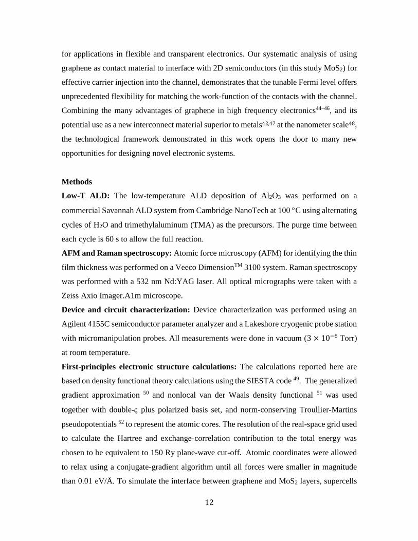
Figure 1. (a) Optical micrograph and AFM data (inset) of a single-layer (SL) chemical
vapor deposition (CVD) grown MoS2 thin film. (b) Raman spectroscopy of as-grown SL
CVD MoS2 thin film (red line) and the CVD graphene/ MoS2 structure. (c) Schematic
illustration of important fabrication steps to make large-scale electronics from
graphene/MoS2 heterostructure using MoS2 as channel and graphene as contact electrodes
and interconnects. (d) Optical micrograph (left) and AFM (right) of CVD MoS2 dual gate
18
transistor with graphene as electrodes. The scale bar in AFM image is 10 µm. (e) Optical
micrograph of large-scale chip of MoS2 devices and circuits using CVD graphene as
electrodes and interconnects (white dashed box) as well as control devices and circuits
using Ti/Au electrodes in adjacent (red dashed box). Metal pads (gold color) are
fabricated on the sample for convenient measurement. The scale bar is 500 µm.
19
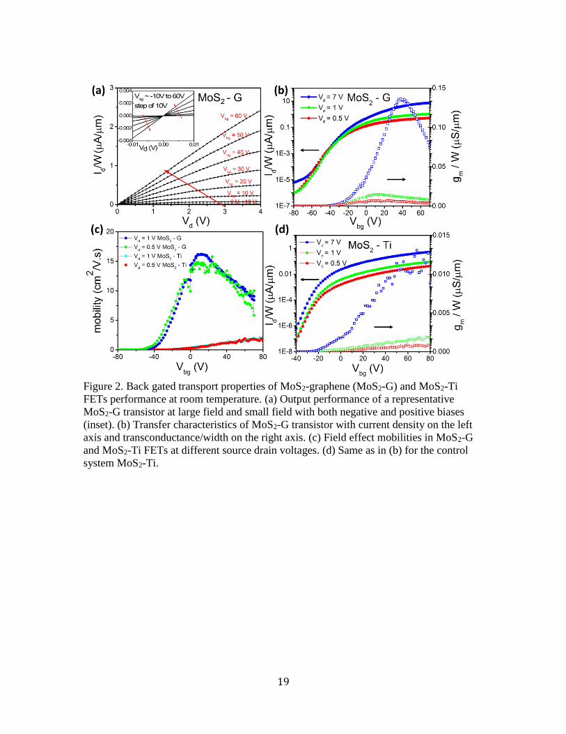
Figure 2. Back gated transport properties of MoS2-graphene (MoS2-G) and MoS2-Ti
FETs performance at room temperature. (a) Output performance of a representative
MoS2-G transistor at large field and small field with both negative and positive biases
(inset). (b) Transfer characteristics of MoS2-G transistor with current density on the left
axis and transconductance/width on the right axis. (c) Field effect mobilities in MoS2-G
and MoS2-Ti FETs at different source drain voltages. (d) Same as in (b) for the control
system MoS2-Ti.
20
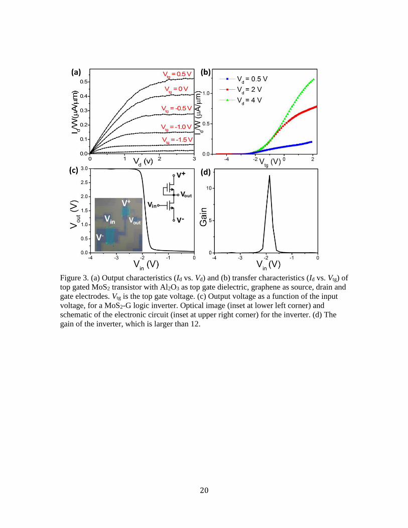
Figure 3. (a) Output characteristics (Id vs. Vd) and (b) transfer characteristics (Id vs. Vtg) of
top gated MoS2 transistor with Al2O3 as top gate dielectric, graphene as source, drain and
gate electrodes. Vtg is the top gate voltage. (c) Output voltage as a function of the input
voltage, for a MoS2-G logic inverter. Optical image (inset at lower left corner) and
schematic of the electronic circuit (inset at upper right corner) for the inverter. (d) The
gain of the inverter, which is larger than 12.
21
Figure 4. Temperature dependent transport, that is, Id-Vbg curves at various temperatures,:
(a) and (b) MoS2-G FET, (c) and (d) MoS2-Ti FET. The source drain bias for both
structures are 0.5 V during measurement. In (b) and (d) we show the linear fit of
Arrhenius plot ln(𝐼d 𝑇3/2⁄ )) vs. 1000 𝑇⁄ .
22
Figure 5. (a) Schottky barrier height 𝜑𝐵 (in meV) and corresponding error bars, as a
function of the gate bias Vbg (in V) for CVD grown MoS2-G and MoS2-Ti junctions. (b)
Experimental setup used (upper panel) and schematic band diagram of MoS2/G
heterostructure at Vbg=0 and Vbg > 0 (bottom panel). The corresponding edges of the
valence band (VB) and the conduction band (CB) are shown, with EF marked by the dashed
line. (c) Calculated band structures of MoS2/-Graphene interface at zero bias and doping
(left), zero bias with finite doping concentration (11.05x1012 cm-2) (middle) and 80 V back
gate bias at the same doping (right). 𝜑𝐵 is indicated by the vertical arrow pointing from EF
to the CB minimum at the K point. The relevant graphene and MoS2 states are shown by
blue and red lines, respectively. (d) Calculated 𝜑𝐵 (in meV) as a function of the bias
voltage Vbg (in V) at different doping levels. The horizontal red line at 400 meV shows the
value of the 𝜑𝐵 expected from the difference between the work function of graphene (4.5
23
eV) and the electron affinity of MoS2 (~4.1 eV). The red dots show the experimental results