Graphene on Ru(0001) Moire Corrugation Studied by ScanningTunneling Microscopy on Au/Graphene/Ru(0001) HeterostructuresR. Cortes,† D. P. Acharya,†,§ C. V. Ciobanu,‡ E. Sutter,† and P. Sutter*,†
†Center for Functional Nanomaterials, Brookhaven National Laboratory, Upton, New York 11973, United States‡Department of Mechanical Engineering & Materials Science Program, Colorado School of Mines, Golden, Colorado 80401, UnitedStates
*S Supporting Information
ABSTRACT: Two-dimensional Au islands of different thicknessesgrown on graphene/Ru(0001) were used to study the corrugation ofthe moire structure of graphene/Ru(0001) and discriminate betweenits mainly structural or electronic character. A comparison of theapparent corrugation measured by scanning tunneling microscopy(STM) for different Au thicknesses with results of elasticity theoryequations applied to a gold film over a corrugated substrate shows thatthe corrugation observed for the graphene/Ru(0001) moire is ofstructural nature rather than electronic. STM showed a large value forthe corrugation of the first Au monolayer on graphene/Ru(0001), 1.7 Å; using density functional theory calculations, we explainthis large corrugation of the Au monolayer as the result of a strong (weak) binding of the Au layer at the valley (hill) regions ofthe graphene/Ru(0001) moire structure and infer an actual corrugation of the graphene/Ru(0001) moire structure of ∼1.2 Åfrom the measured corrugation of the Au monolayer.
■ INTRODUCTION
Graphene has attracted enormous attention in recent years dueto its exceptional properties and its prospective applications inelectronics, photonics, energy generation and storage, andsensing, among others.1 The development of most of theseapplications requires synthesis processes able to produce large-area single-crystalline graphene domains. Epitaxial growth ontransition metals has become a promising method for large-scale graphene synthesis.2−5 In this context, the epitaxial growthof graphene on Ru allows the formation of truly macroscopicsingle-crystalline domains.2 The lattice mismatch betweengraphene and Ru gives rise to the formation of a long-rangeordered moire pattern, which periodically modifies thegraphene properties (e.g., the chemical reactivity) and isobserved as a periodic corrugation in scanning tunnelingmicroscopy (STM) images.6 Moire-induced modifications canbe beneficial as they allow, for example, using graphene as atemplate for the adsorption of metal nanoclusters7−9 andorganic molecules,10,11 but a deeper understanding of the moire structure is still needed.Despite the large volume of published work dealing with the
graphene/Ru(0001) moire structure, the origin of the periodicmoire observed by STM remains controversial. It is well-knownthat STM images reflect both the surface topography and thenear-surface electronic structure, and the two contributions canbe difficult to separate in practice. In STM measurements ongraphene/Ru(0001), the apparent corrugation of the moire structure is highly dependent on the tunneling bias voltage,12
changing from ∼1 to ∼−0.7 Å (i.e., inverted contrast) in the−3 to +3 V sample bias range. This, together with helium atom
scattering (HAS) experiments,12 which showed a small surfacecorrugation in the range 0.15−0.4 Å, led to the conclusion thatthe corrugation observed by STM is mainly of electronic originand that the actual topography of the graphene/Ru(0001)surface is nearly flat. In contrast, a much larger geometricalcorrugation, 1.5 Å, was obtained by quantitative low-energyelectron diffraction (LEED)-I(V) analysis.13 Surface X-raydiffraction (SXRD) measurements gave two different val-ues,14,15 1.5 and 0.82 Å . Finally, density functional theory(DFT) calculations not including the effect of van der Waals(vdW) interactions16−19 gave a corrugation in the range 1.5−1.7 Å, while later DFT calculations with vdW corrections20,21
showed that these corrections reduce the computed corrugationto 1.2−1.3 Å . These calculations suggest that vdW interactionsplay an important role at the moire maxima, where the distancebetween graphene and the Ru surface is close to the interlayerdistance in graphite, whereas they are less important at themoire valleys due to the rather strong covalent interactionbetween graphene and Ru at those regions.22
Au evaporated onto monolayer graphene/Ru(0001) wets thesurface of the graphene layer and forms well-defined two-dimensional (2D) islands,7,19,23,24 which we find to have arange of thicknesses from one to several atomic layers. STMimages of the surface of these 2D Au islands show a corrugatedperiodic structure similar to that of the bare graphene/Ru(0001) moire, notably consisting of a hill-and-valley
Received: June 28, 2013Revised: September 9, 2013Published: September 16, 2013
morphology with the same in-plane periodicity as the graphenemoire. The observation of a corrugation at the surface of thin2D Au islands suggests that the graphene/Ru(0001) moire structure corrugation is an actual morphological feature and notmerely an electronic effect. In this case, it is reasonable toexpect that a thin, wetting Au film would conform to thecorrugation of the substrate and that the resulting heightvariations at the surface of a few monolayer thick Au islandshould be attenuated with increasing Au thickness according tothe elastic properties of Au. Therefore, we used in this work Auislands of different thicknesses grown on monolayer graphene/Ru(0001) to study the corrugation of the graphene/Ru(0001)moire structure and to discriminate between its mainlystructural or mainly electronic origin; specifically, we comparedthe apparent surface corrugation measured by STM and itschange with increasing Au thickness with calculations of theexpected corrugation and its change considering a sinusoidallycorrugated substrate covered by a thin film with the elasticproperties of Au. Our results support the notion that thecorrugation of the graphene/Ru(0001) moire is primarily astructural feature. In addition, we observed an enhancedcorrugation for the first Au monolayer that is explained usingdensity functional theory calculations. Combining the measuredcorrugation for a single Au layer with the calculations, we inferthe actual corrugation of the graphene/Ru(0001) moire structure.
■ METHODSGraphene was epitaxially grown on Ru(0001) in ultrahighvacuum (UHV) by C surface segregation as described in detailelsewhere.2 Briefly, a clean Ru(0001) single crystal wasenriched with interstitial C by ethylene exposure at atemperature higher than 1000 °C. Subsequent slow loweringof the sample temperature caused C surface segregation drivingthe graphene growth. Au was deposited on the graphene/Ru(0001) surface at room temperature by thermal evaporationfrom a Au drop suspended by a W filament. Samples werestudied in situ by STM using a Createc low-temperature STMoperated at 77 K. In order to decide whether the corrugationobserved in the Au films deposited on graphene/Ru(0001) is amainly electronic effect or an actual morphological feature, weanalyzed the measured corrugation at the surface of 2D Auislands with different thicknesses and compared the results withelastic continuum calculations for a Au film conforming to asinusoidally corrugated substrate. In the calculations, we solvedthe equilibrium elastic equations for thin Au films with imposedsinusoidal out-of-plane displacements on the bottom surfaceand with zero normal stress on the upper surface. Theseequations were cast in terms of the components of thedisplacement field, and we solved them using a Papkovitch−Neuber solution form in which the displacement componentswere expressed as combinations of harmonic functions, whichwere subsequently determined from the boundary conditions. Ifthe corrugation is a true morphological feature of the Au filmdeposited on epitaxial graphene, then the computed out-of-plane displacement on the upper surface of the Au film and itschange with film thickness should, at least qualitatively, matchour STM measurements.In order to assess the nature of the bonding of Au to the
graphene/Ru(0001) system, we also performed density func-tional theory (DFT) calculations in the local (spin) densityapproximation (LDA).25,26 In these calculations, we usedprojector-augmented wave pseudopotentials27 and the Ceper-
ley−Alder exchange-correlation functional.28 The cutoff for theplane wave energy was 700 eV, the Brillouin zone was sampledusing a 5 × 5 × 1 Monkhorst−Pack grid, the vacuum spacingbetween the periodic slabs was 15 Å, and the geometryrelaxations were stopped when residual forces decreased below0.01 eV/Å. The DFT calculations for model Au/graphene/Ru(0001) systems show a significant change in the binding ofAu when placed on graphene/Ru(0001) in comparison to Auon free-standing graphene. We used the results from thesemodel calculations to explain the observed enhancedcorrugation of the Au monolayer on graphene/Ru(0001).Finally, we performed large-scale molecular statics calculationsto check that the presence of the first Au monolayer does notmodify the corrugation of the underlying graphene/Ru(0001).These calculations were performed using the LAMMPSsimulation package.29 The interactions of Au atoms weredescribed by embedded-atom potentials30 and those of C atomsby Tersoff potentials.31
■ RESULTS
Samples prepared in the described way present a densedistribution of stepped Au islands with different areas andthicknesses, as shown in the overview STM image of Figure 1a.The smallest thickness observed is ∼3.4 Å, in contrast with the5.5 Å thick Au islands that have been reported previously.19,23
The periodic corrugation characteristic of the moire structure of
Figure 1. Morphology of room temperature deposited Au onmonolayer graphene/Ru(0001), observed by UHV STM at 77 K.(a) Overview STM image showing Au islands of different heights(Vsample = −0.27 V, I = 0.46 nA). Circles mark islands whose terracesare partially or completely flat. (b) Close-up view of one of the islandswith two different Au terrace heights (Vsample = −0.45 V, I = 0.43 nA).A moire-like structure is visible in both of them as well as in thesurrounding graphene surface not covered by Au. (c) Height profilesalong the lines marked in (b), corresponding to a bare grapheneterrace (A), a 1 ML Au terrace (B), and a 2 ML Au terrace (C).
The Journal of Physical Chemistry C Article
dx.doi.org/10.1021/jp406415h | J. Phys. Chem. C 2013, 117, 20675−2068020676
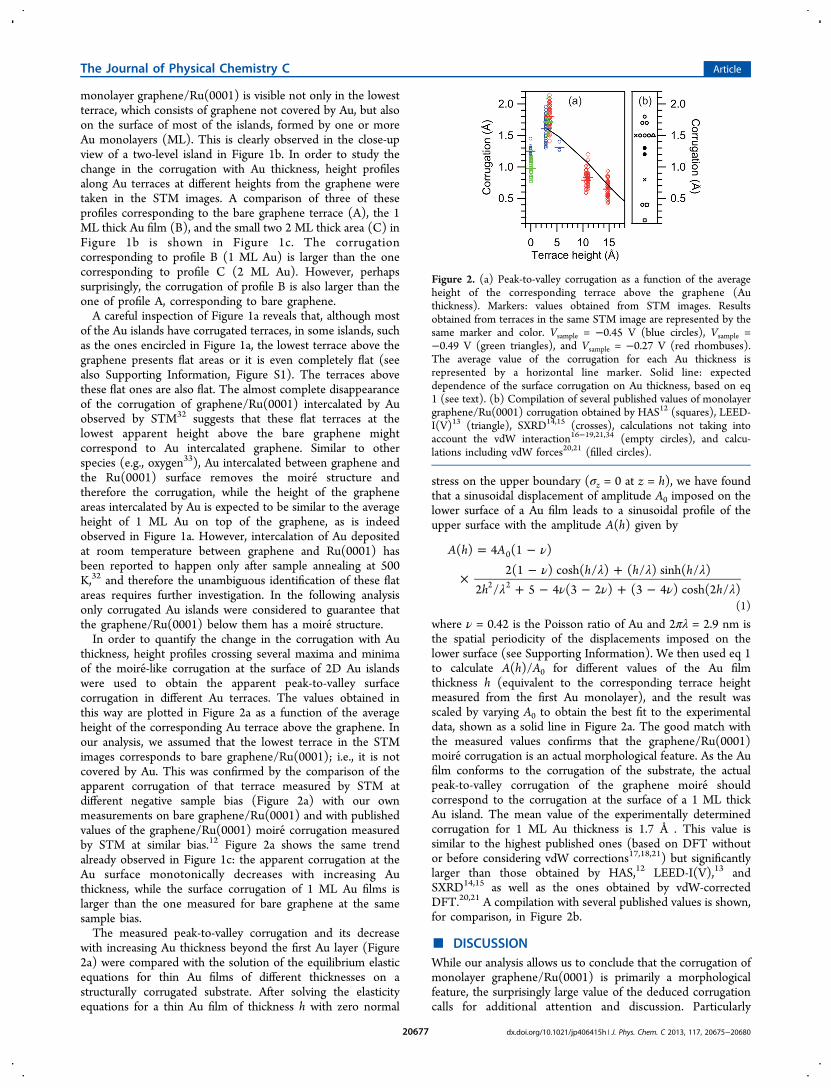
monolayer graphene/Ru(0001) is visible not only in the lowestterrace, which consists of graphene not covered by Au, but alsoon the surface of most of the islands, formed by one or moreAu monolayers (ML). This is clearly observed in the close-upview of a two-level island in Figure 1b. In order to study thechange in the corrugation with Au thickness, height profilesalong Au terraces at different heights from the graphene weretaken in the STM images. A comparison of three of theseprofiles corresponding to the bare graphene terrace (A), the 1ML thick Au film (B), and the small two 2 ML thick area (C) inFigure 1b is shown in Figure 1c. The corrugationcorresponding to profile B (1 ML Au) is larger than the onecorresponding to profile C (2 ML Au). However, perhapssurprisingly, the corrugation of profile B is also larger than theone of profile A, corresponding to bare graphene.A careful inspection of Figure 1a reveals that, although most
of the Au islands have corrugated terraces, in some islands, suchas the ones encircled in Figure 1a, the lowest terrace above thegraphene presents flat areas or it is even completely flat (seealso Supporting Information, Figure S1). The terraces abovethese flat ones are also flat. The almost complete disappearanceof the corrugation of graphene/Ru(0001) intercalated by Auobserved by STM32 suggests that these flat terraces at thelowest apparent height above the bare graphene mightcorrespond to Au intercalated graphene. Similar to otherspecies (e.g., oxygen33), Au intercalated between graphene andthe Ru(0001) surface removes the moire structure andtherefore the corrugation, while the height of the grapheneareas intercalated by Au is expected to be similar to the averageheight of 1 ML Au on top of the graphene, as is indeedobserved in Figure 1a. However, intercalation of Au depositedat room temperature between graphene and Ru(0001) hasbeen reported to happen only after sample annealing at 500K,32 and therefore the unambiguous identification of these flatareas requires further investigation. In the following analysisonly corrugated Au islands were considered to guarantee thatthe graphene/Ru(0001) below them has a moire structure.In order to quantify the change in the corrugation with Au
thickness, height profiles crossing several maxima and minimaof the moire-like corrugation at the surface of 2D Au islandswere used to obtain the apparent peak-to-valley surfacecorrugation in different Au terraces. The values obtained inthis way are plotted in Figure 2a as a function of the averageheight of the corresponding Au terrace above the graphene. Inour analysis, we assumed that the lowest terrace in the STMimages corresponds to bare graphene/Ru(0001); i.e., it is notcovered by Au. This was confirmed by the comparison of theapparent corrugation of that terrace measured by STM atdifferent negative sample bias (Figure 2a) with our ownmeasurements on bare graphene/Ru(0001) and with publishedvalues of the graphene/Ru(0001) moire corrugation measuredby STM at similar bias.12 Figure 2a shows the same trendalready observed in Figure 1c: the apparent corrugation at theAu surface monotonically decreases with increasing Authickness, while the surface corrugation of 1 ML Au films islarger than the one measured for bare graphene at the samesample bias.The measured peak-to-valley corrugation and its decrease
with increasing Au thickness beyond the first Au layer (Figure2a) were compared with the solution of the equilibrium elasticequations for thin Au films of different thicknesses on astructurally corrugated substrate. After solving the elasticityequations for a thin Au film of thickness h with zero normal
stress on the upper boundary (σz = 0 at z = h), we have foundthat a sinusoidal displacement of amplitude A0 imposed on thelower surface of a Au film leads to a sinusoidal profile of theupper surface with the amplitude A(h) given by
νν λ λ λ
λ ν ν ν λ
= −
× − ++ − − + −
A h Ah h h
h h
( ) 4 (1 )2(1 ) cosh( / ) ( / ) sinh( / )
2 / 5 4 (3 2 ) (3 4 ) cosh(2 / )
0
2 2
(1)
where ν = 0.42 is the Poisson ratio of Au and 2πλ = 2.9 nm isthe spatial periodicity of the displacements imposed on thelower surface (see Supporting Information). We then used eq 1to calculate A(h)/A0 for different values of the Au filmthickness h (equivalent to the corresponding terrace heightmeasured from the first Au monolayer), and the result wasscaled by varying A0 to obtain the best fit to the experimentaldata, shown as a solid line in Figure 2a. The good match withthe measured values confirms that the graphene/Ru(0001)moire corrugation is an actual morphological feature. As the Aufilm conforms to the corrugation of the substrate, the actualpeak-to-valley corrugation of the graphene moire shouldcorrespond to the corrugation at the surface of a 1 ML thickAu island. The mean value of the experimentally determinedcorrugation for 1 ML Au thickness is 1.7 Å . This value issimilar to the highest published ones (based on DFT withoutor before considering vdW corrections17,18,21) but significantlylarger than those obtained by HAS,12 LEED-I(V),13 andSXRD14,15 as well as the ones obtained by vdW-correctedDFT.20,21 A compilation with several published values is shown,for comparison, in Figure 2b.
■ DISCUSSIONWhile our analysis allows us to conclude that the corrugation ofmonolayer graphene/Ru(0001) is primarily a morphologicalfeature, the surprisingly large value of the deduced corrugationcalls for additional attention and discussion. Particularly
Figure 2. (a) Peak-to-valley corrugation as a function of the averageheight of the corresponding terrace above the graphene (Authickness). Markers: values obtained from STM images. Resultsobtained from terraces in the same STM image are represented by thesame marker and color. Vsample = −0.45 V (blue circles), Vsample =−0.49 V (green triangles), and Vsample = −0.27 V (red rhombuses).The average value of the corrugation for each Au thickness isrepresented by a horizontal line marker. Solid line: expecteddependence of the surface corrugation on Au thickness, based on eq1 (see text). (b) Compilation of several published values of monolayergraphene/Ru(0001) corrugation obtained by HAS12 (squares), LEED-I(V)13 (triangle), SXRD14,15 (crosses), calculations not taking intoaccount the vdW interaction16−19,21,34 (empty circles), and calcu-lations including vdW forces20,21 (filled circles).
The Journal of Physical Chemistry C Article
dx.doi.org/10.1021/jp406415h | J. Phys. Chem. C 2013, 117, 20675−2068020677
puzzling are the increase in the corrugation of the first Aumonolayer with respect to that of graphene and its large value,which suggest that the interaction of Au with different regionsof the moire pattern of graphene/Ru(0001) acts so as toamplify the corrugation of the Au monolayer.Graphene interacts weakly with Ru at the hills and strongly at
the valley regions,20 as shown schematically in Figure 3.
Therefore, at the hill regions, the interactions betweengraphene and Au layer are not significantly affected by thepresence of Ru below graphene; in those regions, the distancebetween Au and graphene layers may be estimated on the basisof DFT calculations for graphene on a Au substrate, d1 ≃ 3.31Å, with a weak binding of 80 meV per Au atom at the surface(or 30 meV/C atom).35 Using DFT calculations for a single Aumonolayer and (2 × 2) graphene cells with the experimentallattice constant of 2.46 Å, we have predicted the interlayerdistance to be d1 = 3.26 Å and a binding energy between Aumonolayer and graphene of 97 meV/Au atom. We use a similardefinition for binding energy as that of ref 35. The bindingenergy between the Au monolayer and graphene (or graphene/Ru system) is defined as the difference, per Au atom, betweenthe total energy of a system in which the Au layer is far fromgraphene (or from graphene/Ru) and the total energy of Au/graphene (or Au/graphene/Ru) relaxed to attain theequilibrium distance between the layers.Assuming that the corrugation of graphene is not
significantly altered upon the deposition of Au, the corrugationof the Au monolayer, AAu, can be related to that of graphene,Agr, via AAu = Agr + d1 − d2, where d2 is the distance betweenthe Au and graphene layers in the valley region (Figure 3). Wehave calculated the distance d2 and the interaction between Auand graphene/Ru(0001) in the valleys using DFT calculationsperformed on a (2 × 2) Ru(0001) substrate at the experimentallattice constants of Ru (a = 2.70 Å, c/a = 1.584). The choice forthis supercell (shown in Figure 4) is determined by the fact thatover significant portions of the valleys in the graphene/Ru(0001) moire superstructure pairs of C atoms of thegraphene lattice are one on top of the Ru atom and the other inthe hollow site at the surface.20 The locations of the Au atomsare such that the system is minimally strained while stillcommensurate (by necessity in DFT calculations) with thegraphene/Ru(0001) system.35 The binding energy of the Aumonolayer that we calculated is 199 meV/Au atom. Thedistance between the Au monolayer and the graphene layer isd2 = 2.73 Å; this is the difference between the average height ofthe Au atoms and that of the C atoms. The values of the
binding energy and the Au−graphene interlayer distance areconsistent with a chemical bonding between the Au layer andthe graphene/Ru(0001) that is significantly stronger thantypical vdW interactions. As seen in Figure 4, two of the threeAu atoms in the supercell (those located directly above Catoms) are bonded to C. Although one of the Au atoms is notchemically bonded to the graphene/Ru(0001), on average thebinding between Au and C remains very strong and effectivelyclamps down the Au layer at the valley regions of the moire structure, thus increasing its corrugation. With the valuescalculated for the spacings d1 (Au on graphene far away fromRu) and d2 (Au on graphene/Ru(0001) in the valleys of themoire structure) the corrugation of the Au monolayer (Figure3) is AAu = Agr + d1 − d2 = Agr + 0.53 Å, i.e., ∼0.5 Å larger thanthe one of bare graphene/Ru(0001).The inability of STM to provide reliable values of the
geometrical corrugation for the complex surface structure ofgraphene/Ru(0001), due to strong electronic effects,12 hasmotivated the use of Au layers in our study. The electroniceffects are expected to be much less important for a 2D Aulayer wetting the graphene/Ru(0001) moire because, due toeffective screening, the electronic properties of Au thin filmsadsorbed on graphene/Ru(0001) are mainly determined by theelectronic structure of the Au adlayers and are essentiallyindependent of the electronic structure of the substrate.36
Hence, the main contribution to the tunneling current for Au/graphene/Ru(0001) comes from the electronic density of statesof Au and is independent of the one of graphene/Ru(0001).The apparent height of few-layer Au films might be affected byquantum well states confined to Au. However, this would notchange the corrugation measured on a specific Au terrace,where the Au thickness is constant due to the 2D growth of Auon graphene/Ru.7,24 Therefore, STM images of Au thin filmson graphene/Ru(0001) can be used to quantitatively study thesurface corrugation, in contrast to the STM images on baregraphene/Ru(0001). Using the measured amplified corrugationof the Au monolayer (∼1.7 Å) and the results of our DFT
Figure 3. Schematic illustration of a corrugated Au monolayerdeposited on graphene/Ru(0001). In the hill regions, the distancebetween Au and graphene is d1, while in the flat valley regions thedistance is d2. The spacings d1 and d2 relate the corrugation AAu of theAu monolayer to that of the underlying graphene/Ru (Agr) via AAu =Agr + d1 − d2.
Figure 4. Top and side view of the relaxed Au/graphene/Ru(0001)system. The supercell vectors in the plane of the surface are indicatedby the black arrows on the top view. The Au layer is chemicallybonded to graphene/Ru(0001), with a binding energy of 199 meV/Auatom and an interlayer spacing of d2 = 2.73 Å. The Au atoms areshown smaller than the C atoms so as to aid the visualization of theirlocations with respect to graphene and Ru.
The Journal of Physical Chemistry C Article
dx.doi.org/10.1021/jp406415h | J. Phys. Chem. C 2013, 117, 20675−2068020678
calculations, we can infer the actual corrugation of the baregraphene/Ru(0001) to be Agr = AAu − 0.53 Å = 1.2 Å.In the above reasoning for deriving the corrugation of
graphene/Ru(0001) from that of a Au layer deposited on it, wemade the assumption that the presence of the Au monolayerdoes not affect the corrugation of the underlying graphene/Ru(0001) system. A posteriori, we tested this assumption usinglarge-scale molecular statics calculations in which a Au layer isbrought in the vicinity of an already corrugated graphene sheet,and the interactions between Au atoms and C atoms aremodeled by Lennard-Jones potentials parametrized accordingto our DFT results for binding energies and interlayer distancesdescribed above. More specifically, the Lennard-Jones potentialis modified to have a finite cutoff radius, and the parametersused for the strongly binding C interaction to Au are ε = 0.2eV, σ = d2/2
1/6 = 2.432 Å, and rcut = 4.0 Å, while thosecorresponding to the weak C−Au interactions are ε = 0.097 eV,σ = d1/2
1/6 = 2.90 Å, and rcut = 12.0 Å. Any model potentialthat incorporates the weak (strong) interactions between Auand graphene at the hills (valleys) of the moire superstructuresuffices for understanding the overall morphological features ofAu on corrugated graphene; in particular, this is a clear andefficient way to tell whether the corrugation of the grapheneitself is changed upon the deposition of the Au monolayer. TheAu layer relaxes toward the corrugated graphene starting at adistance of 5 Å and complies to graphene in the mannerdescribed by Figure 3. The physical reason for this compliance(as opposed to, e.g., flattening the graphene so as to maximizethe area of stronger, chemical bonding) is that the epitaxialrelationship of graphene with the Ru substrate (e.g., ref 20)simply does not allow the graphene to be flat throughout.The value of the corrugation of graphene/Ru(0001) inferred
here from the measured corrugation of the Au monolayer, ∼1.2Å, lies in between the two published values obtained bySXRD14,15 and is smaller that most of the values provided bycalculations not including vdW corrections16−19,21 (Figure 2),while it is in agreement with the published values obtained byDFT calculations with vdW corrections.20,21 This highligts theimportance of vdW interactions in defining the corrugatedgraphene/Ru(0001) moire structure.
■ CONCLUSIONS
In conclusion, the comparison of the measured corrugation of2D Au layers with varying thickness on graphene/Ru(0001)with calculations shows that the moire structure of graphene onRu(0001) is strongly geometrically corrugated. The surprisinglylarge value (∼1.7 Å) obtained for the surface corrugation of asingle Au monolayer on graphene/Ru(0001) is explained byDFT calculations, which show that a different interactionstrength of Au with the hills and valleys of the graphene/Ru(0001) moire amplifies the corrugation of the Au monolayer.From these calculations and the experimentally measuredcorrugation of the Au monolayer, a corrugation of thegraphene/Ru(0001) moire of ∼1.2 Å is obtained.
■ ASSOCIATED CONTENT
*S Supporting InformationClose-up views of STM image showing islands whose terracesare partially or completely flat; deduction of eq 1. This materialis available free of charge via the Internet at http://pubs.acs.org.
Present Address§D.P.A.: Global Foundries, Malta, NY 12020.
NotesThe authors declare no competing financial interest.
■ ACKNOWLEDGMENTS
This research has been carried out at the Center for FunctionalNanomaterials, Brookhaven National Laboratory, which issupported by the U.S. Department of Energy, Office of BasicEnergy Sciences, under Contract DE-AC02-98CH10886.C.V.C. was supported by Contract 114940 from BNL and byNSF Grant CMMI-0846858. The DFT calculations wereperformed with resources from the Golden Energy ComputingOrganization. We also thank Abbas Ebnonnasir for setting upthe molecular statics calculations.
■ REFERENCES(1) Novoselov, K. S.; Fal’ko, V. I.; Colombo, L.; Gellert, P. R.;Schwab, M. G.; Kim, K. A Roadmap for Graphene. Nature 2012, 490,192−200.(2) Sutter, P. W.; Flege, J.-I.; Sutter, E. A. Epitaxial Graphene onRuthenium. Nat. Mater. 2008, 7, 406−411.(3) Li, X.; Cai, W.; An, J.; Kim, S.; Nah, J.; Yang, D.; Piner, R.;Velamakanni, A.; Jung, I.; Tutuc, E.; Banerjee, S. K.; Colombo, L.;Ruoff, R. S. Large-Area Synthesis of High-Quality and UniformGraphene Films on Copper Foils. Science 2009, 324, 1312−1314.(4) Reina, A.; Jia, X.; Ho, J.; Nezich, D.; Son, H.; Bulovic, V.;Dresselhaus, M. S.; Kong, J. Large Area, Few-Layer Graphene Films onArbitrary Substrates by Chemical Vapor Deposition. Nano Lett. 2009,9, 30−35.(5) Sutter, P.; Sadowski, J. T.; Sutter, E. Graphene on Pt(111):Growth and Substrate Interaction. Phys. Rev. B 2009, 80, 245411.(6) Marchini, S.; Gunther, S.; Wintterlin, J. Scanning TunnelingMicroscopy of Graphene on Ru(0001). Phys. Rev. B 2007, 76, 075429.(7) Zhou, Z.; Gao, F.; Goodman, D. W. Deposition of Metal Clusterson Single-Layer Graphene/Ru(0001): Factors That Govern ClusterGrowth. Surf. Sci. 2010, 604, L31−L38.(8) N’Diaye, A. T.; Bleikamp, S.; Feibelman, P. J.; Michely, T. Two-Dimensional Ir Cluster Lattice on a Graphene Moire on Ir(111). Phys.Rev. Lett. 2006, 97, 215501.(9) Sutter, E.; Albrecht, P.; Wang, B.; Bocquet, M.-L.; Wu, L.; Zhu,Y.; Sutter, P. Arrays of Ru Nanoclusters with Narrow Size DistributionTemplated by Monolayer Graphene on Ru. Surf. Sci. 2011, 605, 1676−1684.(10) Mao, J.; Zhang, H.; Jiang, Y.; Pan, Y.; Gao, M.; Xiao, W.; Gao,H.-J. Tunability of Supramolecular Kagome Lattices of MagneticPhthalocyanines Using Graphene-Based Moire Patterns as Templates.J. Am. Chem. Soc. 2009, 131, 14136−14137.(11) Zhou, H.; Zhang, L.; Mao, J.; Li, G.; Zhang, Y.; Wang, Y.; Du,S.; Hofer, W.; Gao, H.-J. Template-Directed Assembly of PentaceneMolecules on Epitaxial Graphene on Ru(0001). Nano Res. 2013, 6,131−137.(12) Borca, B.; Barja, S.; Garnica, M.; Minniti, M.; Politano, A.;Rodriguez-García, J. M.; Hinarejos, J. J.; Farías, D.; de Parga, A. L. V.;Miranda, R. Electronic and Geometric Corrugation of PeriodicallyRippled, Self-Nanostructured Graphene Epitaxially Grown onRu(0001). New J. Phys. 2010, 12, 093018.(13) Moritz, W.; Wang, B.; Bocquet, M.-L.; Brugger, T.; Greber, T.;Wintterlin, J.; Gunther, S. Structure Determination of the CoincidencePhase of Graphene on Ru(0001). Phys. Rev. Lett. 2010, 104, 136102.(14) Martoccia, D.; Willmott, P. R.; Brugger, T.; Bjorck, M.; Gunther,S.; Schleputz, C. M.; Cervellino, A.; Pauli, S. A.; Patterson, B. D.;
The Journal of Physical Chemistry C Article
dx.doi.org/10.1021/jp406415h | J. Phys. Chem. C 2013, 117, 20675−2068020679
Marchini, S.; Wintterlin, J.; Moritz, W.; Greber, T. Graphene onRu(0001): A 25 × 25 Supercell. Phys. Rev. Lett. 2008, 101, 126102.(15) Martoccia, D.; Bjorck, M.; Schleputz, C. M.; Brugger, T.; Pauli,S. A.; Patterson, B. D.; Greber, T.; Willmott, P. R. Graphene onRu(0001): A Corrugated and Chiral Structure. New J. Phys. 2010, 12,043028.(16) Wang, B.; Bocquet, M.-L.; Marchini, S.; Gunther, S.; Wintterlin,J. Chemical Origin of a Graphene Moire Overlayer on Ru(0001). Phys.Chem. Chem. Phys. 2008, 10, 3530−3534.(17) Wang, B.; Bocquet, M.-L.; Gunther, S.; Wintterlin, J. Commenton “Periodically Rippled Graphene: Growth and Spatially ResolvedElectronic Structure”. Phys. Rev. Lett. 2008, 101, 099703.(18) Jiang, D.-E.; Du, M.-H.; Dai, S. First Principles Study of theGraphene/Ru(0001) Interface. J. Chem. Phys. 2009, 130, 074705.(19) Xu, Y.; Semidey-Flecha, L.; Liu, L.; Zhou, Z.; Goodman, D. W.Exploring the Structure and Chemical Activity of 2-D Gold Islands onGraphene Moire/Ru(0001). Faraday Discuss. 2011, 152−76.(20) Stradi, D.; Barja, S.; Díaz, C.; Garnica, M.; Borca, B.; Hinarejos,J. J.; Sanchez-Portal, D.; Alcamí, M.; Arnau, A.; Vazquez de Parga, A.L.; Miranda, R.; Martín, F. Role of Dispersion Forces in the Structureof Graphene Monolayers on Ru Surfaces. Phys. Rev. Lett. 2011, 106,186102.(21) Wang, B.; Bocquet, M.-L. Interfacial Coupling in RotationalMonolayer and Bilayer Graphene on Ru(0001) from First Principles.Nanoscale 2012, 4, 4687−4693.(22) Sutter, P.; Hybertsen, M. S.; Sadowski, J. T.; Sutter, E.Electronic Structure of Few-Layer Epitaxial Graphene on Ru(0001).Nano Lett. 2009, 9, 2654−2660.(23) Liu, L.; Zhou, Z.; Guo, Q.; Yan, Z.; Yao, Y.; Goodman, D. W.The 2-D Growth of Gold on Single-Layer Graphene/Ru(0001):Enhancement of CO Adsorption. Surf. Sci. 2011, 605, L47−L50.(24) Wang, B.; Bocquet, M.-L. Monolayer Graphene and h-BN onMetal Substrates as Versatile Templates for Metallic Nanoclusters. J.Phys. Chem. Lett. 2011, 2, 2341−2345.(25) Kresse, G.; Furthmuller, J. Efficient Iterative Schemes for AbInitio Total-Energy Calculations Using a Plane-Wave Basis Set. Phys.Rev. B 1996, 54, 11169−11186.(26) Kresse, G.; Furthmuller, J. Efficiency of Ab-Initio Total EnergyCalculations for Metals and Semiconductors Using a Plane-Wave BasisSet. Comput. Mater. Sci. 1996, 6, 15−50.(27) Kresse, G.; Joubert, D. From Ultrasoft Pseudopotentials to theProjector Augmented-Wave Method. Phys. Rev. B 1999, 59, 1758−1775.(28) Ceperley, D.; Alder, B. Ground State of the Electron Gas by aStochastic Method. Phys. Rev. Lett. 1980, 45, 566−569.(29) Plimpton, S. Fast Parallel Algorithms for Short-Range MolecularDynamics. J. Comput. Phys. 1995, 117, 1−19.(30) Daw, M. S.; Baskes, M. I. Embedded-Atom Method: Derivationand Application to Impurities, Surfaces, and Other Defects in Metals.Phys. Rev. B 1984, 29, 6443−6453.(31) Tersoff, J. Modeling Solid-State Chemistry: InteratomicPotentials for Multicomponent Systems. Phys. Rev. B 1989, 39,5566−5568.(32) Huang, L.; Pan, Y.; Pan, L.; Gao, M.; Xu, W.; Que, Y.; Zhou, H.;Wang, Y.; Du, S.; Gao, H.-J. Intercalation of Metal Islands and Films atthe Interface of Epitaxially Grown Graphene and Ru(0001) Surfaces.Appl. Phys. Lett. 2011, 99, 163107.(33) Sutter, P.; Sadowski, J. T.; Sutter, E. A. Chemistry under Cover:Tuning Metal-Graphene Interaction by Reactive Intercalation. J. Am.Chem. Soc. 2010, 132, 8175−8179.(34) Pan, Y.; Zhang, H.; Shi, D.; Sun, J.; Du, S.; Liu, F.; Gao, H.-J.Highly Ordered, Millimeter-Scale, Continuous, Single-CrystallineGraphene Monolayer Formed on Ru (0001). Adv. Mater. 2009, 21,2777−2780.(35) Khomyakov, P. A.; Giovannetti, G.; Rusu, P. C.; Brocks, G.; vanden Brink, J.; Kelly, P. J. First-Principles Study of the Interaction andCharge Transfer between Graphene and Metals. Phys. Rev. B 2009, 79,195425.
(36) Yakovkin, I. N. Band Structure of Au Layers on the Ru(0001)and Graphene/Ru(0001) Surfaces. Eur. Phys. J. B 2012, 85, 61.
The Journal of Physical Chemistry C Article
dx.doi.org/10.1021/jp406415h | J. Phys. Chem. C 2013, 117, 20675−2068020680