40
GRAPHENE How this wonder material is transforming every industry 1N. Franklin St. Suite 1850, Chicago, IL 60606, USA, Phone: (872) 222-9225. Email: [email protected] Spring 2015
GRAPHENEHow this wonder material is transforming every industry
1N. Franklin St. Suite 1850, Chicago, IL 60606, USA, Phone: (872) 222-9225. Email: [email protected]
Spring 2015

2
Graphene, an atomically-thin, two-dimensional layer of carbon, has been touted as a miracle material: in addition to being incredibly strong, light and flexible, it can act as a flexible semiconductor. As a result, it has been a major focus of scientific research and popular interest. Over the next decade, the European Union plans to fund more than €1 billion of research into graphene, and the raw material market for graphene is expected to exceed $390 million by 2024. Sales of products containing graphene are expected to top $1.3 billion over the same interval.
Yet, in 2013, all suppliers of graphene were small, privately-held companies. Difficulties in producing high purity samples of graphene have created a situation where graphene remains remarkably underutilized in industry. While companies like Apple, Samsung, Nokia, and IBM have made significant investments in applied graphene research, the vast majority of companies have yet to investigate ways in which graphene could impact their business.
While research and development programs are expensive, the cost of inaction can be staggering. Graphene is predicted to be as influential and disruptive as the microprocessor. Companies like Blockbuster, Commodore, Polaroid, and Borders serve as stark examples of how a failure to innovate and adopt new technology can cause a thriving business to wither, and ultimately collapse. Graphene’s fascinating material properties will quickly usher in an era of strong, lightweight, flexible devices that will quickly make today’s cutting-edge devices into obsolete relics of a former age.
This report serves as a primer on graphene. It summarizes key milestones in the development of graphene, highlights the state of current manufacturing techniques, and separates fact from myth in popular science articles. It illustrates coming trends, and showcases ways in which a variety of industries are already exploring the impact of graphene. If you know you need to investigate graphene, but aren’t sure where to start, this report will quickly bring you up to speed and enable you make actionable, intelligent decisions that will leverage graphene as effectively as possible in your business.
Editors’ Note
1 N. Franklin St. Chicago, IL 60606, USA Phone: (872) 222-9225. Email: [email protected]
Paul Elliott & Justin Starr
3
Table of Contents
Seminal Graphene Work- The early days, and the first methods of graphene isolation 04
Single Layer (Two-Dimensional) Materials 06
Graphene: Fact vs. Myth 09
Graphene Research and Production 14
How to Isolate Graphene from Graphite at Home 17
Graphene’s Global Market and Research 21
Flexible Electronics 24
Energy Production and Storage 26
Industrial Applications 30
Interview with DR. AMAIA ZURUTUZA, Scientific Director at Graphenea 35
Graphene Facts 39

4
Seminal Graphene Work- The early days, and the first methods of graphene isolationAki Ueda
They donated a simple cellophane tape dispenser and a small hunk of graphite to the Nobel Museum. These two humble items were gifts from Andre Geim, and Konstantin Novoselov, the 2010 winners of the Nobel Prize in Physics. These items were the tools integral to Geim’s and Novoselov’s 2004 discovery of a method to produce near-monolayers of graphene. This molecular film is destined to revolutionize research materials, electronic and communications equipment, and a wide-range of industrial activities.
In 1859 the president of the Royal Chemical Society, Benjamin Collins Brodie, wrote a memoir titled “On the Atomic Weight of Graphite in the Philosophical Transactions.” In this memoir Brodie coined the term “Graphon,” stating that its structural qualities, and its role as a building block of graphite, formed a “determinate atomic weight (33)”.
In the early 1900’s Thomas Edison visualized the “paper-like” film, which builds into blocks of graphite as a highly valuable material. But it was Edison’s assistant Edward Acheson that first devised a method to manufacture a near-pure form of graphite. Although the properties of graphene and its potential uses have long been speculated, reliable methods of isolating single layers of graphene were not readily available until well into the 21st century.
Graphene is a naturally occurring material. Like diamond, it is composed of carbon atoms arranged in a crystalline structure. But graphene is more resilient than diamond, it is about 200 times stronger than steel, and conducts electricity more efficiently than copper, yet it is remarkably flexible due to its sheet-like molecular film structure.
In essence, graphite is composed of stacks upon stacks of layers of graphene, which is a flat, sheet-like structure of carbon atoms arranged in a hexagonal lattice pattern. In fact, anyone who has written with a common school pencil--the lead of which is composed of graphite--has sheared off multi-layers of graphene in the process. The unique electronic properties of graphene, however, are
Graphene - Seminal Graphene Work- The early days, and the first methods of graphene isolation
Graphite Monolayers of Graphene

5
only fully realized when the compound is isolated into monolayer sheets of the crystalline carbon structure. This effectively produces a two-dimensional material that is one carbon-atom thick.
In 2004, Geim and Novoselov, working at the University of Manchester, made seminal steps toward isolating monolayers of graphene, and demonstrated its stability and utility in electrical applications. Their method, which they described in their 2004 publication in Science, was attractively elegant. At the time, many graphene laboratories, including that of Gein and Novoselov, used common cellophane tape to clean off the surface of the graphite sample of interest. This tape was normally then discarded without an afterthought. However, one Friday, during a relaxed night in the lab, the scientists realized that the cellophane tape actually held graphene, which with consecutive peelings could be reduced to fewer and fewer layers of the carbon compound. Eventually Geim and Novoselov yielded a single graphene monolayer. This graphene monolayer isolation process is now known as the “Cellophane-tape,” or the “Mechanical exfoliation method.”
Even though the knowledge and research regarding graphene, or “Graphon,” has existed for over a century, it was this elegant method of isolating the graphite monolayers that revolutionized the field. This revelation sparked new research. It enabled scientist to conduct new generation research of graphite, or graphene. This research led 21st Century science to investigate a wide range of innovative and interesting graphene applications.
To acknowledge their discovery, Geim and Novoselov were awarded the 2010 Nobel Prize for Physics.
FURTHER READING:
Isolating GrapheneNovoselov, K. S. et al. Electric field effect in atomically thin carbon films. Science 306, 666–669 (2004).
Graphene - Seminal Graphene Work- The early days, and the first methods of graphene isolation

6
Single Layer (Two-Dimensional)MaterialsCharles Wright
According to James Horne professor of mechanical engineering at Columbia University, graphene is the strongest and thinnest material ever discovered. It is as flexible as rubber and more transparent than glass, and it exhibits high electrical and thermal conductivity. Although the field of graphene science is relatively new, as compared to the science of other types of carbon, graphene already lays claim to an astonishing number of superlatives.
The many incarnations of carbon atoms range from the everyday hard transparent diamond, to soft and sooty graphite, to the exotic soccer-ball shaped buckyball, to the tiny cylindrical nanotube. Pure- carbon atoms can be combined in a variety of structural configurations, or allotropes. With the exception of diamond, the basic structural unit of each of these substances is a hexagon. They are composed of six covalently bonded carbon atoms, known as a benzene ring. When this motif is tiled along two-dimensions in a one-atom thick sheet, graphene is formed.
Derived from the Latin word “carbo” or coal, carbon has a total of six electrons. With two of these electrons protected in the atomic inner shell, it leaves four electrons in the outer shell. These electrons are readily available for chemical reaction, and are what make graphene so unique.
In graphene the honeycomb lattice is covalently bound to three coplanar neighboring atoms. This configuration leaves one leftover electron in the third dimension, above and below the plane. The chemically reactive edges form vacancies in the structure’s molecular make-up that quickly fill with neighboring electrons to create a high-quality crystal lattice. The near-perfect two-dimensional structure with very tightly bound, in-plane, atoms and the one highly mobile out-of-plane atom , gives graphene its amazing properties.
One of these properties is its considerable mechanical strength. The very small but impressively strong covalent carbon bonds, uninterrupted by defects, give graphene a tensile strength approximately 200 times greater than that of steel. These small covalent bonds also contribute to graphene’s impressive elasticity.
A sheet of graphene is exactly one atom thick, and can be stressed and stretched to 20-percent of its given shape in either direction and still snap back to its initial size after the strain is removed.. The extreme thinness also provides an interesting optical property: a sheet of graphene is transparent
Single Layer (Two-Dimensional) Materials

7
and lets up to 97.7-percent of the incoming light in the visible spectrum through. Compare this to about 90-percent for a sheet of clear glass, and the optical properties of graphene become even more accessible. In other words, it is practically invisible. Finally, the combination of stiff covalent bonds and reduced dimensionality act to minimize dissipation in the propagation of thermal vibrations, which makes graphene a superb heat conductor as well.
Another superlative of graphene results from its extraordinary ability to conduct electricity. The potential applications as a result of this superlative could be nearly limitless. Due to the lack of lattice imperfections, unlike the imperfections scientists find in metals for example, electrons can travel unimpeded through graphene, without being scattered off course and losing energy in the Second Law of Thermodynamics. At room temperature, the intrinsic mobility of electrons in graphene is 100 times greater than the levels found in silicon. In addition, the current-carrying electrons have negligible mass, meaning that they travel enormously fast. Just 300 times less than the speed of light, and thus obey relativistic quantum mechanics. For this reason, graphene nanoribbons could carry 1000 times more current than conventional copper interconnects.
The highly mobile free π electrons in graphene’s planar configuration that is held together by strong covalent bonds, add a number of fascinating superlative properties to the substance. Researchers are just beginning to understand and harness these properties for a wide variety of uses. The substance’s extreme versatility means that slight modifications often extend its range of adaptability. For example, graphene has no band gap and is therefore a poor semiconductor, but it can be converted into a high quality semiconductor by adding a bilayer of graphene and applying an electric field.
Single Layer (Two-Dimensional) Materials
8
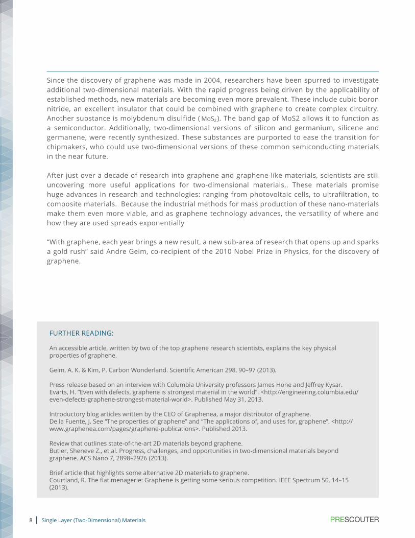
Since the discovery of graphene was made in 2004, researchers have been spurred to investigate additional two-dimensional materials. With the rapid progress being driven by the applicability of established methods, new materials are becoming even more prevalent. These include cubic boron nitride, an excellent insulator that could be combined with graphene to create complex circuitry. Another substance is molybdenum disulfide ( ). The band gap of MoS2 allows it to function as a semiconductor. Additionally, two-dimensional versions of silicon and germanium, silicene and germanene, were recently synthesized. These substances are purported to ease the transition for chipmakers, who could use two-dimensional versions of these common semiconducting materials in the near future.
After just over a decade of research into graphene and graphene-like materials, scientists are still uncovering more useful applications for two-dimensional materials,. These materials promise huge advances in research and technologies: ranging from photovoltaic cells, to ultrafiltration, to composite materials. Because the industrial methods for mass production of these nano-materials make them even more viable, and as graphene technology advances, the versatility of where and how they are used spreads exponentially
“With graphene, each year brings a new result, a new sub-area of research that opens up and sparks a gold rush” said Andre Geim, co-recipient of the 2010 Nobel Prize in Physics, for the discovery of graphene.
FURTHER READING:
An accessible article, written by two of the top graphene research scientists, explains the key physical properties of graphene.
Geim, A. K. & Kim, P. Carbon Wonderland. Scientific American 298, 90–97 (2013).
Press release based on an interview with Columbia University professors James Hone and Jeffrey Kysar.Evarts, H. “Even with defects, graphene is strongest material in the world”. <http://engineering.columbia.edu/even-defects-graphene-strongest-material-world>. Published May 31, 2013.
Introductory blog articles written by the CEO of Graphenea, a major distributor of graphene.De la Fuente, J. See “The properties of graphene” and “The applications of, and uses for, graphene”. <http://www.graphenea.com/pages/graphene-publications>. Published 2013.
Review that outlines state-of-the-art 2D materials beyond graphene.Butler, Sheneve Z., et al. Progress, challenges, and opportunities in two-dimensional materials beyond graphene. ACS Nano 7, 2898–2926 (2013).
Brief article that highlights some alternative 2D materials to graphene. Courtland, R. The flat menagerie: Graphene is getting some serious competition. IEEE Spectrum 50, 14–15 (2013).
Single Layer (Two-Dimensional) Materials

9
Graphene: Fact vs. MythMatt DeJarld
Wild claims about graphene’s revolutionary capabilities have floated around media outlets since its isolation in 2004. Every couple of months a tech magazine or science blog disseminates information about a new groundbreaking application for the near-monolayer substance. Even after a decade of research and fabrication this wonder-technology is still under strict scrutiny. According to Google Trends, the percentage of online searches for graphene related information has increased 5-fold since 2009. But like most scientific breakthroughs that achieve public fame and recognition, the field of graphene science is inundated from the outside with delusional thinking.
Among the five major revolutionary possibilities for the application of graphene, one misconception is that graphene will replace silicon in computer chips.
In the public’s eye, graphene is tightly linked to computers and tech gadgets. In bilayers, graphene has astounding electronic properties as a semiconducting material. While these attributes are great
Graphene: Fact vs. Myth

10
in theory and measurement, research concerning graphene based-transistors conducted at Boston University, in conjunction with the Instituto de Ciencia de Materials in Madrid, and the Center of Physics at the Universidade de Minho in Braga, Portugal, has uncovered a flaw in graphene’s application for computer chips. While graphene has very low resistance and excellent thermal properties, it has difficulty “switching off.” Due to its zero band gap the on-off current ratio is very poor. Even in the “off” state, graphene transistors transfer a large amount of current, and a device made solely in this fashion would be impractical and wasteful. However, transistors have been made using graphene. Xiangfeng Duan at the University of California Los Angeles reported in 2013 that a self-aligned graphene transistor is scalable and has a
cutoff frequency of around 427 GHz.
Despite efforts to improve the on-off ratio through nanofabrication methods, graphene transistors still cannot compare to silicon-based transistors. Some researchers claim they can solve the on-off issue by inducing a band gap with graphene bilayers or utilizing certain biasing schemes to produce negative differential resistances. Nevertheless, these solutions have yet to be proven in a convincing and scalable manner. Due to these innate flaws, it is safe to say that graphene is not going to replace silicon anytime soon. Even though graphene can boast record speeds of conductivity, unless the “off “ current can be reduced, it will never become a practical alternative to silicon for everyday computer chip applications. Most likely future computing devices will consist of a mixture of silicon and graphene materials, incorporating the best attributes of both.
A second misrepresentation distributed by the media about the physical properties of graphene concerns its tensile strength and elastic modulus as compared to steel.
In 2008, Dr. Lee Bollinger, President of the Department of Mechanical Engineering at Columbia University, stated that graphene is the strongest material ever measured. The elastic modulus of graphene is 1,000 gigapascals (GPa), and its ultimate tensile strength is, respectively, 130 GPa. For comparison purposes, standard steel has an elastic modulus of 200 GPa, and an ultimate tensile strength of, respectively, 550 megapascals. In other words, graphene has an ultimate tensile strength 200 times that of steel! However, this does not mean that graphene is going to replace steel girders in buildings and bridges. To understand why, it is important to fully appreciate the concept of the “strength” and the “size” of graphene as compared to steel, and put both materials into their appropriate context.
Graphene: Fact vs. Myth
11
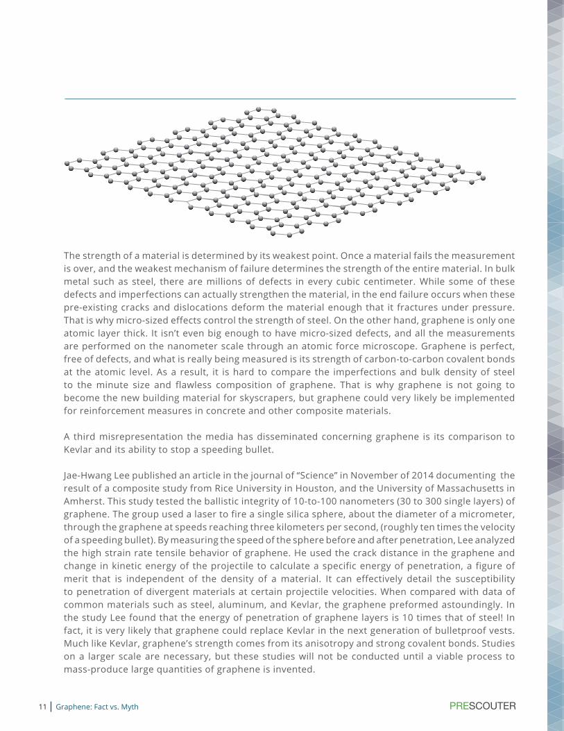
The strength of a material is determined by its weakest point. Once a material fails the measurement is over, and the weakest mechanism of failure determines the strength of the entire material. In bulk metal such as steel, there are millions of defects in every cubic centimeter. While some of these defects and imperfections can actually strengthen the material, in the end failure occurs when these pre-existing cracks and dislocations deform the material enough that it fractures under pressure. That is why micro-sized effects control the strength of steel. On the other hand, graphene is only one atomic layer thick. It isn’t even big enough to have micro-sized defects, and all the measurements are performed on the nanometer scale through an atomic force microscope. Graphene is perfect, free of defects, and what is really being measured is its strength of carbon-to-carbon covalent bonds at the atomic level. As a result, it is hard to compare the imperfections and bulk density of steel to the minute size and flawless composition of graphene. That is why graphene is not going to become the new building material for skyscrapers, but graphene could very likely be implemented for reinforcement measures in concrete and other composite materials.
A third misrepresentation the media has disseminated concerning graphene is its comparison to Kevlar and its ability to stop a speeding bullet.
Jae-Hwang Lee published an article in the journal of “Science” in November of 2014 documenting the result of a composite study from Rice University in Houston, and the University of Massachusetts in Amherst. This study tested the ballistic integrity of 10-to-100 nanometers (30 to 300 single layers) of graphene. The group used a laser to fire a single silica sphere, about the diameter of a micrometer, through the graphene at speeds reaching three kilometers per second, (roughly ten times the velocity of a speeding bullet). By measuring the speed of the sphere before and after penetration, Lee analyzed the high strain rate tensile behavior of graphene. He used the crack distance in the graphene and change in kinetic energy of the projectile to calculate a specific energy of penetration, a figure of merit that is independent of the density of a material. It can effectively detail the susceptibility to penetration of divergent materials at certain projectile velocities. When compared with data of common materials such as steel, aluminum, and Kevlar, the graphene preformed astoundingly. In the study Lee found that the energy of penetration of graphene layers is 10 times that of steel! In fact, it is very likely that graphene could replace Kevlar in the next generation of bulletproof vests. Much like Kevlar, graphene’s strength comes from its anisotropy and strong covalent bonds. Studies on a larger scale are necessary, but these studies will not be conducted until a viable process to mass-produce large quantities of graphene is invented.
Graphene: Fact vs. Myth
12
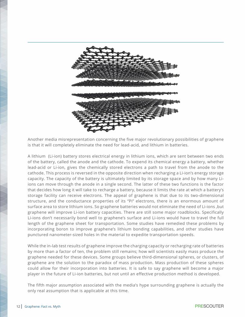
Another media misrepresentation concerning the five major revolutionary possibilities of graphene is that it will completely eliminate the need for lead-acid, and lithium in batteries.
A lithium (Li-ion) battery stores electrical energy in lithium ions, which are sent between two ends of the battery, called the anode and the cathode. To expend its chemical energy a battery, whether lead-acid or Li-ion, gives the chemically stored electrons a path to travel from the anode to the cathode. This process is reversed in the opposite direction when recharging a Li-ion’s energy storage capacity. The capacity of the battery is ultimately limited by its storage space and by how many Li-ions can move through the anode in a single second. The latter of these two functions is the factor that decides how long it will take to recharge a battery, because it limits the rate at which a battery’s storage facility can receive electrons. The appeal of graphene is that due to its two-dimensional structure, and the conductance properties of its “Pi” electrons, there is an enormous amount of surface area to store lithium ions. So graphene batteries would not eliminate the need of Li-ions ,but graphene will improve Li-ion battery capacities. There are still some major roadblocks. Specifically Li-ions don’t necessarily bond well to graphene’s surface and Li-ions would have to travel the full length of the graphene sheet for transportation. Some studies have remedied these problems by incorporating boron to improve graphene’s lithium bonding capabilities, and other studies have punctured nanometer-sized holes in the material to expedite transportation speeds.
While the in-lab test results of graphene improve the charging capacity or recharging rate of batteries by more than a factor of ten, the problem still remains; how will scientists easily mass produce the graphene needed for these devices. Some groups believe third-dimensional spheres, or clusters, of graphene are the solution to the paradox of mass production. Mass production of these spheres could allow for their incorporation into batteries. It is safe to say graphene will become a major player in the future of Li-ion batteries, but not until an effective production method is developed.
The fifth major assumption associated with the media’s hype surrounding graphene is actually the only real assumption that is applicable at this time.
Graphene: Fact vs. Myth

13
The process of converting salt water into drinking water involves using a semipermeable membrane; which is a thin molecular film that allows water molecules to pass through it, but does not allow the NaCl molecules to pass through. Current technology uses thin molecular film composites that require a significant amount of pressure to push the water through. The pressure is a needed factor, because the films, though comparatively small are still comparatively thick as compared to graphene. By perforating the sheet of graphene with nanometer-sized holes, the graphene sheet can allow water molecules to pass through but not the NaCl ions. In fact, Lockheed Martin already has a membrane in development named “Perforene”®, and they are ramping up production to implement in saltwater filters. There are some issues with tearing of the graphene sheet, but Lockheed scientists are working on fixing that problem. That is why graphene is expected to make a heavy impact on the desalination market, in the near future.
FURTHER READING:
Electronic PropertiesNeto, A., Guinea, F., Peres, N. M. R., Novoselov, K. S. & Geim, A. K. The electronic properties of graphene. Rev. Mod. Phys. 81, 109–162 (2009).
Strength of GrapheneLee, C., Wei, X., Kysar, J. W., & Hone, J. Measurement of the elastic properties and intrinsic strength of monolayer graphene. Science 321, 385-388 (2008).
Ballistic TestsLee, J. H., Loya, P. E., Lou, J., & Thomas, E. L. Dynamic mechanical behavior of multilayer graphene via supersonic projectile penetration. Science 346, 1092-1096 (2014).
Graphene BatteriesLiu, Y., Artyukhov, V. I., Liu, M., Harutyunyan, A. R., & Yakobson, B. I. Feasibility of Lithium Storage on Graphene and Its Derivatives. J. Phys. Chem. Lett. 4, 1737-1742 (2013).
DesalinationCohen-Tanugi, D., & Grossman, J. C. Water desalination across nanoporous graphene. Nano Lett. 12, 3602-3608 (2012).
Graphene: Fact vs. Myth
14
Graphene Research and ProductionAki Ueda
Ever since Andre Geim and Konstantin Novoselov discovered graphene in 2004, scientists around the world have been racing toward developing reliable cost-effective methods to mass-produce the material. Graphene production research is continuously moving forward, looking toward reducing costs, increasing yields, purity, and eliminating material and energy waste. Newer methods aim to produce a better synthetic graphene, reliably generating large amounts of monocrystalline graphene from scratch.
We are now living in the dawn of the graphene industry. It’s full potential could range as far as the human imagination. But realizing this full potential relies on bringing graphene production out of the laboratory setting, and into the commercial world.
A successful method to mass-produce industrial graphene must quickly and cheaply generate large amounts of the compound, while maintaining high purity and structural integrity in the final product. Depending on the application, the sheet size and the crystalline make-up become highly relevant in achieving this goal.
Commercial graphene is generally found in two forms: monocrystalline and polycrystalline layers. Polycrystalline graphene is suitable for application as a composite mixed with other materials. One polycrystalline application uses graphene mixed with silicon in the manufacture of transistors.
Graphene Research and Production
15
A suitable utilization for monocrystalline layers of graphene applies it as a molecular-film to touchscreens and solar cells.
While polycrystalline graphene can be “grown” from carbon components using deposition techniques, monocrystalline graphene could initially only be derived by removing the graphene layers from its graphite precursor. The latter method is difficult to scale upwards, thereby posing technical limitations on the supply of monocrystalline graphene, as well as its downstream applications.
So far scientists have used two main methods to synthesize graphene. The first method takes advantage of graphite, the natural source of graphene. This method isolates the crystalline monolayers from graphite’s physical structure, the method that led Geim and Novoselov to the Nobel Prize in 2010. The alternative method is to fabricate or grow polycrystalline graphene using elemental carbon atoms. This method promotes the development of graphene through various procedures that create its crystalline structure. But research is booming.
Multiple methods are being developed to better isolate graphene from graphite, making large strides from the days when Cellophane tape was used as the method of isolation. Electrically charged glass allows for more precise measures, control, and reproducibility. Scientists have explored the concept of exfoliation by photons or liquids, followed by a liquid gradient isolation.
On the other end of the research spectrum, scientists are exploring methods for “growing” synthetic graphene from its base component, carbon. An early method involved using the crystalline structure of silicon carbide (SiC) as a surrogate-of-sorts, causing the carbon atoms to arrange themselves into a lattice structure. Other methods scientist are using involves precipitation from a mixture of graphene and molten metal, as well as deposition from a chemical vapor of carbon onto a metal substrate. These methods generate graphene from scratch and yield fairly high qualities. But they consume a large amount of energy and produce a variety of waste products. Moreover, these methods have only been capable of producing polycrystalline graphene, which is limited in applicability compared to its monocrystalline relative.
In the scientific quest to create a cost-effective near-pure monolayer of graphene, Samsung, in collaboration with Sungkyunkwan University in South Korea, has recently unveiled a method of producing a monocrystalline synthetic. The method involves chemical vapor deposition of monocrystalline graphene onto silicon wafers coated with germanium. The germanium here is key; it provides a unidirectional substrate so that graphene crystals grow unidirectionally, and eventually fuse into one monocrystalline layer. The successive application of this new method will very likely be incorporated into the next generation of Samsung cell phones, batteries, and other small wearable electronic gadgets.
Samsung is by no means alone in the scientific quest to isolate or synthesize monocrystalline graphene. In September 2014 Thomas Mallouk, Professor of Chemistry and Molecular Biology at Pennsylvania State University, and Nina Kovtyukhova published their method of isolating graphene from graphite in the journal of Nature Chemistry. This revolutionary concept uses “guest molecules or ions” that insert themselves between the layers of graphene inside the larger substrate of
Graphene Research and Production

16
graphite. These molecules work as a wedge, wedging those layers apart. The eventual result is monocrystalline layers of graphene.
Jonathan Coleman, Professor of Chemical Physics, Keith Paton of the Thomas Swan Company, and a team of young scientists at Trinity College’s Centre for Research on Adaptive Nanostructures and Nanodevices, or the CRANN Institute, in Dublin, Ireland discovered yet another method to isolate monocrystalline layers of graphene from graphite. The team of scientists was able to isolate the graphene, without damaging it, using the force of agitation created by a spinning rotor in a liquid medium. The process causes the graphene sheets to break off of the graphite. The liquid compound stabilizes
these sheets of graphene and keeps them, like the initial breakthrough using Cellophane tape, from sticking back together.
Unlike the original method introduced by Geim and Novoselov, the methods being used by scientists in Ireland and Pennsylvania are scalable, and applicable to isolate graphene from graphite for mass production. Groundbreaking research such as these will only continue to progress, moving us ever closer to the new age of accessible and cost-effective graphene technologies.
FURTHER READING:
Research in Graphene ProductionBonaccorso, F, Lombardo, A, Hasan, T & Sun, Z. Production and processing of graphene and 2d crystals. Mater. Today 15, 564-589 (2012).
Producing Monocrystalline Synthetic GrapheneLee, JH et al. Wafer-scale growth of single-crystal monolayer graphene on reusable hydrogen-terminated germanium. Science 344, 286-289 (2014).
Isolating Individual Graphene SheetsKovtyukhova, NI, Wang, Y, Berkdemir, A & Cruz-Silva, R. Non-oxidative intercalation and exfoliation of graphite by Brønsted acids. Nat. Chem. 6, 957-963 (2014).
Paton, KR, Varrla, E, Backes, C, Smith, RJ & Khan, U. Scalable production of large quantities of defect-free few-layer graphene by shear exfoliation in liquids. Nat. Mater. 13, 624-630 (2014).
Graphene Research and Production

17
How to Isolate Graphene from Graphite at HomeJeremy Stromer
Perhaps what really makes graphene exciting, besides flexible touchscreens, amazing water filtration, better solar cells, and super capacitors, is the fact that this wonder material can be isolated with something as dull and as ordinary as a small piece of office tape.
It is slightly tricky to replicate Andre Geim and Konstantin Novoselov’s Nobel Prize-winning procedure. While the steps may not be complex in nature, young scientists may find the method is a little harder to perfect than it appears. Due to its “simplicity” however, it is actually possible to synthesize graphene at home, using a piece of clear-tape and an ordinary writing pencil.
The only differences between this “at-home” procedure, and the procedure the two Nobel Laureates used to synthesize graphene, are their advanced collegiate degrees, and the expensive laboratory equipment they used. Because, aside from the optical microscope, it takes less than $20 and less than a half hour to replicate the procedure at home.
Materials needed: • Graphite. Raw crystalline, flake or powdered form. Powdered graphite is commonly used in
lubricants. A pencil may also be used to “deposit” graphite on some paper first. However, thepencil method is unlikely to give good quality graphene sheets, but it serves to show simpleproof of the concept.
• Clear adhesive office tape. Different researchers have different preference for what kind. It’sbeen noted that brand-name “Scotch” tape may be too sticky.
• Prophylactic gloves to maintain structural integrity of the tape and the other elements of theexperiment.
• An ordinary piece of white paper (if the pencil method is used).
• Silicon wafer (optional). The wafer is not really necessary to make the graphene. But it isintegral if a persons wants to make the graphene sheets visible.
• Optical microscope greater than100x magnification (is also optional). Again, not necessary toproduce the graphene. But it is necessary to see the graphene.
Graphite
How to Isolate Graphene from Graphite at Home

18
The total time to replicate Geim and Novoselov’s experiment is around thirty minutes. But it may take longer to create higher qualities of the molecular-film.
Steps: Tear off a generous amount of the clear tape: around 5 inches long.
Place graphite onto the sticky-side of the first inch of the five-inch piece of tape. (Using the first left or right inch of the tape is not necessary, but it will facilitate later steps of the isolation process). With crystalline graphite, the tape can be stuck straight to the block. It may be worthwhile to use another piece of tape to first remove contaminates from the surface. For powdered graphite, a small dab about one-fourth of an inch in diameter can be placed directly on the adhesive side of the tape. To try the pencil method, sketch a dark spot about one-half of an inch in diameter, onto a piece of paper and stick the left first h a l f - i n c h of the five inch piece of clear tape firmly to the spot.
1
2
How to Isolate Graphene from Graphite at Home

19
Repeat the previous step several more times using a new space of the tape with every fold. As this step is repeated the graphite layer becomes nearly transparent. Once it becomes totally transparent to the naked eye, it is likely that the algorithm has synthesized a small amount of graphene.
Fold tape over on itself and gently pull the tape back apart. Care needs to be taken with this step. The molecular-film of graphene can get ruined if the tape is aggressively separated or pulled apart too quickly.
To make the graphene visible, transfer it from the sticky tape to a silicon wafer. This is done by gently sticking the area were the transparent graphene is on the tape, to the wafer. Slowly and gently rub the back of the tape to remove any air bubbles, then slowly and gently remove the tape from the wafer.
4
3
5
How to Isolate Graphene from Graphite at Home

20
Place the wafer under an optical microscope. The graphene should have sharp edges and have a purple hue.
Note: In our attempt we were unable to see single layers of graphene. The best we were able to see was a group of many layers. To see individual layers, a better microscope would be required and the thickness of SiO2 on our wafer would need to be adjusted. Additionally, using monochromatic light can aid in viewing graphene.
6
Thick clump of graphene layers on tape.
Single and bilayer of Graphene under optical microscope
10 μm is 0.00000001 m, a measurement on themicroscoping scale, a million times smaller than a meter.
How to Isolate Graphene from Graphite at Home
Source: Graphene Industries

21
Graphene’s Global Market and Research Charles Wright
The graphene research industry is booming. Over 50,000 peer-reviewed articles have been published in the decade since its discovery, and almost one-third of these articles were penned in the last year alone. Scientists describe graphene as the “miracle material” of the 21st century. With potential applications that include flexible computer screens, super-efficient water filtration systems, and ultrafast battery chargers, another of graphene’s superlative applications being explored is in advanced bionic devices. At present, however, graphene is only being used in a handful of products.
The number of worldwide patents related to graphene is nearly doubling each year, and now totals over 10,000 (of which 3,500 are US patents). The US government has funded roughly $18 million in grants for small business innovation and research (SBIR). In the United Kingdom, parliament has promised £61 million for a National Graphene Institute. In Korea, the Korean government has set aside $350 million for graphene research and development. The European Union recently announced a Graphene Flagship program that will receive €1 billion over the next ten years, with the first 30 months of funding (€54 million) allotted to communication technologies and applications in the transport and energy sectors.
Scientific research institutions are creating one-fourth of the current worldwide demand for graphene. While the graphene market is highly fragmented at present, the industrial players fall into three main categories: miners and growers, manufacturers of graphene-based compounds or components, and manufacturers who integrate these pieces into products for the end-users.
Graphene Market (US$ million)
Graphene’s Global Market and Research
Source: IdTechEx
22
Current worldwide sales of graphene-related products are generating roughly $20 million in revenue each year. Several independent graphene company analyses of the market have led graphene advocates to believe that graphene revenues could reach up to $200 million by 2020, and over $1 billion by 2024. This is roughly a 50-percent combined annual growth rate (CAGR), and it is consistent with recent trends for publication, patents, and research spending. There is significant room for growth beyond that point, and as many scientists have estimated, the full commercial potential of graphene will not be realized for another 10-to-20 years.
Although fairly high quality, large-surface area graphene is now feasible, it is manufactured mostly for further scientific research. Many component manufacturers can use cheaper “dirty” graphene that includes other compounds but still retains most of graphene’s desired properties. These compounds are particularly promising as a route for graphene to gain a foothold in a number of markets. At present these composites can more readily compete with the price levels of conventional products. For example, even though the electrical properties of inexpensive graphene oxide powder are not good enough for application in advanced optoelectronic equipment; graphene has found a niche for its use on a conductive paper in DNA analysis.
Samsung, IBM, and SanDisk are the dominant companies, and all have invested heavily across this entire value chain. These giants of technology hold a considerable fraction of early patents on electronic devices that use graphene.
Graphene’s Global Market and Research
23
Electronic applications can use medium-grade graphene, and in the coming years it is likely that the technology giants will include graphene in flexible touchscreens, rewriteable e-paper, and foldable organic LEDs or O-LEDs. High-frequency applications and logic transistors that require high quality graphene are likely only a decade away. Near-term photonic applications include mode-locked lasers and photodetectors. But as noted by Konstantin Novoselov, “Graphene’s full power will only be realized in novel applications, which are designed specifically with this material in mind, rather than when it is used to replace other materials in existing applications”. We should expect such applications, including flexible electronics and improved supercapacitors, to become a reality within the coming decades. However, use of graphene will first become widespread as it is used to make improvements to a wide range of existing products.
The area where the economic world will see the earliest and most rapid uptake of graphene is in composite materials, which capitalize on its structural properties. Additionally, graphene can be added to engine oil to improve lubrication, to paint to reduce corrosion, or to razor blades to improve useful lifetimes. In the past, similar novel materials have taken up to four decades to achieve widespread market uptake--think carbon fiber--or have failed to live up to their potential outside of research, like carbon nanotubes. A range of applications, which, usually only require some subset of its unique features will force graphene into the open market. As technology improves, and mass production becomes a reality, it is predicted that graphene will experience a 70-to-80 percent price drop.
FURTHER READING:
A review article, written by one of the discoverers of graphene, explains the physical properties of graphene and its potential applications, with a critical analysis of their feasibility.Novoselov, K. S., et al. A roadmap for graphene. Nature 490, 192–200 (2012).
A report that analyzes recent developments in the worldwide graphene patent landscape.The Intellectual Property Office of the United Kingdom. “Graphene: The worldwide patent landscape in 2013”. <https://www.gov.uk/government/publications/graphene>. Published March 11, 2013.
A website that contains an up-to-date list of key graphene players in industry, including miners, producers, suppliers, developers, and component manufacturers.Graphene-Info. “Graphene companies: The comprehensive list”. < http://www.graphene-info.com/companies>. Updated 2015.
Graphene’s Global Market and Research

24
Flexible ElectronicsJeremy Stromer
Graphene allows electrons to travel 100 times faster than they can they can travel through a silicon chip. Because graphene’s thermal and electrical conductivity surpasses that of standard silicon and copper, it makes graphene an ideal material for its application in electrical circuits. It has been measured to have 35-percent less resistivity than copper while being able to carry 1,000 times the current. This is accomplished in a substance the size of nanoribbons as compared to the larger substrate of copper. Additionally, its strength and two-dimensional structure give graphene remarkable flexibility. It is allowing researchers to develop flexible circuitry.
Flexible circuitry, on its own, is hardly anything new. Polymer based circuit boards with silver or copper conductors have been around since the 1950s, and
flexible connectors are commonly found in electronics today. However, ultimately, standard flexible circuitry is only bendable to a certain point. Once the circuit undergoes too much deformation, the connections break and the circuit is ruined. By using graphene, however, it seems possible that we may have electronics that are fully bendable and foldable in the near future. Researchers at the Korea Advanced Institute of Science (KAIST) have been able to deposit graphene onto paper to make foldable circuits. A paper-based circuit is advantageous due to its low weight and cost. Multiple institutions have even managed to print graphene based circuits using inkjet printers.
Perhaps, one of the most exciting applications of graphene is its use in flexible touchscreens. Flexible touchscreens could see a wide variety of uses in wearable technology, displays, computers and smart phones. The standard material currently used in touchscreens is Indium Tin Oxide (ITO). ITO is a rigid, transparent conductor, which has also been used in several other applications such as organic light emitting diodes (O-LEDS), solar cells and optical coatings. While ITO does a relatively good job in displays, indium resources are declining and prices are going up. To combat the rising cost of ITO, currently around $1.9 dollars per gram, several other materials have been suggested as replacements: including silver nanowires, conductive polymers, carbon nanotubes and graphene.
Graphene is naturally transparent and has extremely good strength and conductivity as compared with ITO. Raw graphite is low-cost, currently priced at around 0.02¢ cents per gram. These costs, along with graphene’s superlative properties and flexibility make graphene a contender to replace ITO as the go-to material for touchscreens.
Flexible Electronics

25
The benefits of graphene circuits extend beyond that of the current flexible and stretchable design; while transistors are becoming smaller and smaller, getting rid of excess heat is getting harder and harder. Graphene is currently being suggested as a solution to this problem. A 2008 study at the University of California Riverside found graphene to have a thermal conductivity that is about 10 times greater than that of silver or copper. This characteristic will allow for greater heat dissipation, which may be a boon for the computer processing industry.
The strength, thermal, and electrical conductivity of graphene are some of graphene’s most amazing properties and have been measured to be the best of any material currently available. A material with just one of graphene’s many qualities would be useful for a wide array of purposes. However, this special combination allows graphene to be useful for some really incredible applications. Moore’s law is a 1960s prediction that predicted the number of transistors per square inch to double approximately every two years. This prediction has actually managed to hold true for the most part. However, as mass production of graphene becomes a reality, it is starting to look like the fabled Moore’s law may soon no longer be true.
From flexible circuits to foldable touchscreens, graphene will revolutionize the way we think about technology. Its extraordinary characteristics will make graphene an exciting material to watch in the future.
FURTHER READING:
Graphene ApplicationsGeim, AK. Graphene: status and prospects. Science 324, 1530-1534 (2009).
Foldable Paper Based CircuitsHyun, WJ, Park, OO & Chin, BD. Foldable graphene electronic circuits based on paper substrates. Adv. Mater. 25, 4729-4734 (2013).
Heat DissipationGhosh, S, Calizo, I & Teweldebrhan, D. Extremely high thermal conductivity of graphene: Prospects for thermal management applications in nanoelectronic circuits. Appl. Phys. Lett. 92, 151911 (2008).
Conductive Transparent Electrodes/ScreensJurewicz, I, Fahimi, A, Lyons, PE & Smith, RJ. Insulator‐Conductor Type Transitions in Graphene‐Modified Silver Nanowire Networks: A Route to Inexpensive Transparent Conductors. Adv. Funct. Mater. 24, 7580-7587 (2014).
Flexible Electronics

26
Energy Production and StorageMatt DeJarld
Graphene’s potential applications extend to many different technologies in the field of alternative energy: super capacitors, batteries, fuel cells, and photovoltaics. Its geometrical, electrical, and thermal properties make it an excellent addition for the enhancement of current technologies. With increasing global temperatures, rising sea levels, and diminishing fossil fuel supplies, the production and storage of clean energy is becoming exceedingly necessary.
Super capacitorAndrzej Lewandowski at The Poznan University of Technology in Poland theorizes that graphene’s two- dimensional nature allows for many unique phenomena involving thermal and electron transport. One of Lewandowski’s most notable and immediate applications of his theory is the formation of a super capacitor. Capacitors are devices that store electrical energy, but unlike batteries they do not use chemical reagents, discharge almost instantaneously, and overall carry less charge than batteries of the same wright. Super capacitors behave the same way as conventional capacitors, but can hold ten to one hundred times the amount of charge per unit volume. Graphene, in conjunction with its fast electric transport, has a massive amount of surface area for charge storage, giving graphene super capacitors potentially 10,000 times the amount of charging capacity of typical capacitors. Products using graphene superconductors are already on the market, including ultrafast chargers for cellphones and other circuit board electronic components. However, graphene super capacitors will most likely always be used in conjunction with conventional batteries, providing fast charging times when needed, but not as the primary energy source. While they could potentially charge a phone in a few minutes, their total energy storage (per weight) is only a fraction of that of lithium ion (Li-ion) batteries. The maximum energy density of a graphene super capacitor, achieved in a lab setting, is 85.5 Wh/kg. For comparison, Li-ion batteries on the market range between 100-250 Wh/kg and their capacity consistently improving. Nevertheless, graphene based super capacitors will become exceedingly more common in devices as graphene production methods improve.
Lithium-ion batteriesPerhaps the main deterrent to the adoption of electric vehicles is the charging time of electric batteries. While companies such as Tesla Motors have developed batteries that can last hundreds of miles, they still require ample charging time. Even with their supercharging stations, recharging time is around 30 minutes to an hour. This is a long time compared to the five minutes it takes to fill an automobile tank from a gasoline pump. However, recent innovations in battery technology using graphene could reduce charging time and increase the capacity of lithium-ion batteries by a factor of ten or more. As graphene is two-dimensional, there is a significant amount of surface area to hold lithium ions. By adding boron atoms to the graphene, the affinity of the surface for lithium ions is enhanced, thus increasing the chemical charge capacity. Additionally, it was observed that perforating graphene at the anode of the battery vastly improves recharging time, allowing the battery to take full advantage of graphene’s rapid transport properties. Further research has demonstrated that by doping the graphene with either boron or nitrogen allows for both the perforation of graphene and
Energy Production and Storage

27
enhanced Li-ion charging capabilities. This combination of two dimensional structure, doping, and perforation at the anode allows for rapid Li-ion adsorption and ultrafast Li-ion diffusion. Although graphene vastly improves the capabilities of Li-ion devices, currently its incorporation into mass-produced batteries is hindered by inefficient large-scale production methods.
An alternative technique for graphene-equipped Li-ion batteries is the formation of three-dimensional clusters. Some scientists have used a method akin to “deep-frying” to rapidly create little “pom-poms” of graphene. Graphene oxide is submerged in an organic solvent and acid mixture to create fibrous, wavy, graphene balls. While this method doesn’t improve Li-ion charging speeds, it takes advantage of graphene’s massive surface area to greatly improve charging capacity. The advantage of this method is that it is easily scalable, unlike two-dimensional graphene.
Fuel CellsAnother specialized technology where graphene can be utilized for energy storage is fuel cells. Fuel cells, much like batteries, use chemical energy to produce electricity. Whereas the chemical agents of batteries involve metal compounds that are completely enclosed, fuel cells use an agent that is added and removed by an external source. By 2010 graphene research began to focus on graphene’s ability to act in proton exchange membrane fuel cells (PEMFC’s). PEMFC’s convert hydrogen and oxygen into water vapor and harvest the resulting energy. Nitrogen doped graphene is coated with platinum nanoparticles to aid in the reduction of oxygen. The nitrogen defects act as good anchoring sites for the platinum nanoparticles, and fuel cells with power densities of 390-440 were created. For comparison the power density of current PEMFC’s are around 700 . While the
power densities of graphene fuel cells are good, they are not revolutionary. However, recent advancements in graphene fuel cell technology are extremely exciting. Late in 2014 a study conducted by Songnian Hu at the Manchester Center for Mesoscience and Nanotechnology involved investigating the permeability of graphene. Hu discovered that a single layer of graphene could transport protons. It was previously believed that graphene’s dense electron cloud would prevent such transport.
Energy Production and Storage

28
Bilayer graphene does inhibit the transport of protons; however, thermally excited hydrogen ions have been shown to pass through. This opens the potential for graphene to act as a selectively permeable membrane in PEMFC’s. Current PEMFC’s suffer from fuel crossover, severely reducing their efficiency. However, graphene is extremely selective in its permeability, and could drastically improve fuel cell efficiencies. Further research is necessary, but recent discoveries at the Beijing National Laboratory of Molecular Science, and the University of Manchester are very promising.
Photovoltaics
Graphene’s ultrathin, and conductive characteristics are enhancing the photovoltaic market. Photovoltaic cells do not store energy; they harvest energy from the sun by converting photons to electricity. This harvesting is known as clean energy, because it produces very few waste products. While photovoltaics are beginning to compete with fossil fuels and wind energy, they still suffer from high production costs, the creation of waste materials, low efficiencies, and are unable to produce electricity when the sun does not shine or when there is a substantial cloud cover.
A solar cell consists of four layers: a transparent layer,a top electrical contact, a semiconductor layer, which is theactive region or junction between this layer and the fourth layerwhich is the bottom electrical contact. Photons pass through the surface layer, and are collected in the semiconductor
Energy Production and Storage
29
layer, which pushes electrons through the active region. This creates a potential difference between the top and bottom contacts, and electricity is formed. These electrons move through a series of photovoltaic cells connected together by electrodes that work much like anodes and cathodes in a series of batteries. These combined cells are called arrays. Photovoltaic arrays conduct the electricity they harvest into devices that readily use this electricity, or in the more common use, into a storage device such charge a battery. Metals are the most common form of semi-conductive materials used, as they can be easy to apply to most devices. However, in solar cells they can pose a problem because they are not transparent to light! The most common alternative for inclusion in the sub-surface layer is Indium Tin Oxide (ITO), a transparent semiconductor that is used in solar cells requiring complete surface coverage (such as nanowire or colloidal solar cells). While ITO performs well in the sub-surface layer, one of its major constituents, indium, is fairly rare and expensive. Graphene on the other hand can perform the same task with carbon, one of the most abundant elements on earth. Many solar cells in lab settings have already utilized graphene as a top-contact sub-surface layer. Its atomically thin dimensions make it permeable to light and its high conductivity allows for rapid transportation to push electrons through the active region.
FURTHER READING:
Super CapacitorsLewandowski, A., & Galinski, M. Practical and theoretical limits for electrochemical double-layer capacitors. J. Power Sources, 173, 822-828 (2007).Zap & Go Capacitor Cell phone charger Retrieved from http://www.zapandgocharger.com/
Lithium-ion batteriesLiu, Y., Artyukhov, V. I., Liu, M., Harutyunyan, A. R., & Yakobson, B. I. Feasibility of Lithium Storage on Graphene and Its Derivatives. J. Phys. Chem. Lett. 4, 1737-1742 (2013).
Proton exchange membrane fuel cellsZhang, L. S., Liang, X. Q., Song, W. G., & Wu, Z. Y. Identification of the nitrogen species on N-doped graphene layers and Pt/NG composite catalyst for direct methanol fuel cell. Phys. Chem. Chem. Phys. 12, 12055-12059 (2010).
Hu, S et al. Proton transport through one-atom-thick crystals. Nature 516, 227-230 (2014).
PhotovoltaicsWang, X., Zhi, L., & Müllen, K. Transparent, conductive graphene electrodes for dye-sensitized solar cells. Nano lett. 8, 323-327 (2008).
Energy Production and Storage

30
Industrial Applications
The potential for industrial applications of graphene is vast. Nearly every facet of industry can benefit from graphene’s unique properties – often in surprising and unexpected ways. As the properties of graphene become more widely known, it is certain that graphene will find its way into devices, cars, homes and bodies. A subset of this wide range of possibilities is explored in the following sections.
Food and BeverageWhile the food and beverage industry is often slow to incorporate new technologies and materials, a number of graphene applications are coming into fruition. Many packaging materials are being researched that use graphene as a moisture, oxygen and carbon dioxide barrier – properties that can reduce the weight of a package and increase the shelf life of products. Further, many of these barrier properties can be attained with the inexpensive oxidized form of graphene, which is far easier to produce in quantity. Graphene has also been added to plastic bottles in order to make them stronger, lighter than traditional PET bottles. Future products will likely capitalize on the conductive nature of graphene in order to make low-cost active packaging that can display a message or store digital information about a user or product.
Graphene can be used in conjunction with small amounts of metals such as Cu, Ag, and Pt to detect very small amounts of materials. The process used is called Surface-enhanced Raman spectroscopy (SERS) and has been used as an inspection technique for food products. SERS can detect things like pro hibited colorants, toxins, volatile organic compounds, and lactose. SERS with graphene has also
Industrial Applications
Justin Starr

31
been used to detect cholesteral, gluecose, and caffeine in foods, and could enable companies to precisely determine a food product’s contents after it has been prepared, and eliminate counterfeit or tampered products.
Sensors utilizing graphene can also detect airborne molecules to create an “e-nose”. These have been tested to detect vapors released from foods that indicate they are spoiling, such as ethanol, acetone, and methyl acetate. These e-noses can be used to quickly scan an array of food products, and instantly detect items that are nearing spoilage.
Biomedical TechnologyThe surface area of graphene is up to four orders of magnitude higher than other nanomaterials, making it a promising candidate for drug delivery applications. While graphene is not yet approved as a medical device, the FDA has spent more than $1.2 million investigating the safety and toxicity of graphene through programs based at the National Center for Toxological Research and universities around the country, and DARPA has funded a variety of programs that have tested various graphene-based devices in animals.
Despite this, many researchers have developed techniques, structures and methods that are currently being tested in vitro and in vivo in a variety of animals. Researchers at the University of North Carolina, Chapel Hill have developed strips of graphene that can be loaded with doxorubicin and anticancer proteins to serve as targeted chemotherapy agents. Dr. Hongjie Dai at Stanford University has achieved ultrahigh loadings of the anticancer agents SN38 and doxorubicin on sheets of graphene – taking advantage of nearly every exposed atom.
Graphene oxide changes shape in response to a changing environment. In the right conditions, a sheet of graphene oxide can become an array of liquid crystal droplets, with polymer-like properties. Researchers at Monash University are leveraging this technology by using graphene as a targeted drug delivery vehicle, capable of delivering its payload upon encapsulation into a vesicle or other organelle with a unique pH range. These researchers also discovered that these shape changes can be triggered by a magnetic field, further expanding the range of graphene-centric therapies.
This shape changing nature opens the door for graphene to be used as a diagnostic agent. Researchers are investigating how graphene droplets change their shape in the presence of various disease markers. If these structure changes can be consistently and systematically reproduced, graphene could provide a new form of point-of-care diagnostic, when applied to a blood or tissue sample. Further, many shape changes are coupled with a change in range over which graphene fluoresces, meaning many diagnostic uses of graphene could be performed with a simple light source in developing nations.
The high strength of graphene has also led to its use as a reinforcing structure in various biomedical devices. Some research has focused on graphene doped polymers as structures for bone replacement and tissue engineering therapies.
Industrial Applications

32
While many of graphene’s biomedical uses are discovered after months or years of systematic study, some results are arrived at serendipitously. Researchers in China were attempting to make paper-like sheets of graphene for use as scaffolds. Tests of these sheets quickly revealed that human cells were able to attach and grow on these structures, while bacteria were unable to effectively colonize. These results show the promise of graphene films, which are now being explored in live tissue storage, tissue scaffolding, and synthetic bandages or grafts.
Wearable TechnologyGraphene’s flexibility has contributed to its use in a variety of wearable products. Scientists in Ireland have combined graphene with rubber bands in order to create sensors that can easily be applied to any part of the body, and monitor motion, as well as heart rate, and blood oxygen content. These rubber bands, developed by Dr. Jonathan Coleman, are only 0.5% graphene, and can detect strains of less than 0.2%, making the suitable for detecting movements ranging from muscle flexures to microexpressions.
The Cambridge Graphene Center has developed an electrophoretic display consisting of graphene electrodes on a plastic surface. This display is suitable for integration into outerwear, packaging or other articles of clothing, and could form the basis of active clothing that allows users to communicate a dynamically changing message – imagine a shirt that could change its color or pattern on a daily basis. Scientists at Lawrence Berkeley Labs are working on batteries based on graphene oxide,
Industrial Applications
33
suggesting that eventually, a flexible power source could be integrated into active clothing. Further, researchers at Rice University have made flexible graphene supercapacitors using techniques that can be employed outside of a clean room.
The University of Exeter’s Center for Graphene Science has even developed a material known as GraphExeter, which has been heralded by some as an ‘electric cloth’. Researchers there are focusing on ways to make GraphExeter with a spray-on formulation, so that it can quickly be applied to fabrics, windows or other material surfaces. This easily deposited clothing has the potential to retroactively make existing clothing conductive, and suitable for wearable technology.
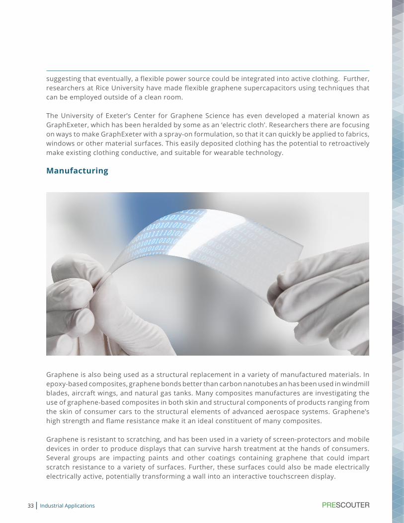
Manufacturing
Graphene is also being used as a structural replacement in a variety of manufactured materials. In epoxy-based composites, graphene bonds better than carbon nanotubes an has been used in windmill blades, aircraft wings, and natural gas tanks. Many composites manufactures are investigating the use of graphene-based composites in both skin and structural components of products ranging from the skin of consumer cars to the structural elements of advanced aerospace systems. Graphene’s high strength and flame resistance make it an ideal constituent of many composites.
Graphene is resistant to scratching, and has been used in a variety of screen-protectors and mobile devices in order to produce displays that can survive harsh treatment at the hands of consumers. Several groups are impacting paints and other coatings containing graphene that could impart scratch resistance to a variety of surfaces. Further, these surfaces could also be made electrically electrically active, potentially transforming a wall into an interactive touchscreen display.
Industrial Applications

34
Other uses of graphene in manufactured products include:• HEAD corporation’s graphene-reinforced, high strength, lightweight tennis rackets• Vorbeck’s Vor-ink, a conductive ink based on dispersed graphene• MeadWestvaco’s antitheft packaging system, based on conductive traces of graphene• Powerbooster’s graphene-based touch screens that have already been deployed on mobile
devices in China.
SummaryWhile graphene has yet to be mass produced on a commercial scale, it is actively being used or investigated in a number of industries. This increased use of graphene has driven production: XG Sciences, a leading producer of graphene, spent $10.5 million in order to increase its annual output of graphene from 3 to 80 tons – an increase of more than 2500%. Ningbo Morsh Technology, a Chinese manufacturer of graphene, invested more than $300 million to create a production line capable of outputting more than 300 tons of graphene annually.
As more and more products utilize graphene, these production increases are expected to continue, decreasing the cost of graphene, and making it suitable for use in a variety of ever cheaper products. The developments mentioned in this section represent the tip of the iceberg, and new uses of graphene are appearing in products on a near-daily basis.
Industrial Applications
FURTHER READING:
General Prospects (2007)Geim, A.K. & Novoselov, K.S. The rise of graphene. Nature, Mater., 6, 183-191 (2007)
Industrial PerspectiveGraphene Uses & Applications. Retrieved from http://www.graphenea.com/pages/graphene-uses-applications
Current Perspective (2014)Focus Issue of Nature Nanotechnology, October 2014, Volume 9, Number 10, Retrieved from http://www.nature.com/nnano/focus/graphene-applications/index.html
Recent DevelopmentsGraphene Industry TrackerRetrieved from http://www.graphenetracker.com/invest/
35
Amaia Zurutuza obtained her PhD in Polymer Chemistry from the University of Strathclyde in Glasgow (UK) in 2002. During her PhD she worked in the research of novel polymers for biomedical applications. After completing her PhD she did two post-doctoral fellowships working within two European projects in the field of molecularly imprinted polymers. At the beginning of 2004, she joined Controlled Therapeutics Scotland Ltd. (UK) where she was a Senior Polymer Scientist working in the R&D of new controlled drug delivery systems. Her research contribution in Controlled Therapeutics lead to the publication of 3 patents in novel biodegradable and biostable polymers for controlling drug delivery. In April 2010 she joined Graphenea as the Scientific Director.
How did you make the transition from polymers to graphene? Well, you could say graphene is also like an infinite polymer made of only carbon atoms, so it was not maybe so hard. Although in reality, because I was used to working in melt processing or solutions, and graphene as you know—the CVD [chemical vapor deposition] process—is gas-phase, it was quite different. Also the techniques to characterize are totally different. So the transition wasn’t so easy, but it was really challenging and interesting nevertheless, so I don’t regret anything to be honest. I lived abroad for many years in Scotland and I was originally from the area near San Sebastián, and I wanted to return. I saw a very interesting ad to be a Scientific Director of a new startup company so I applied. Luckily there were not many people with experience and I got selected and that’s how we started everything. That was almost 5 years ago, so we have worked quite a lot since then. Now we have established processes and we have a lab. We produce graphene to sell it to the research community worldwide. We manufacture everything in Spain, in San Sebastián, and then we ship all over the world.
The current state is that graphene is still a research material. So even if there are some prototypes out there, it’s hard to prove that really they demonstrate improved performance. Maybe it’s more like a marketing thing, for example, like a head racquet, and so on. It’s quite difficult to prove improved performance on something so, not tangible let’s say, but it is expected that graphene will have many applications. And of course, when you mention the term “graphene”, you are not only dealing with one material but a family of materials. So depending on the type and application, the uptake of this
Interview with DR. AMAIA ZURUTUZA, Scientific Director at GrapheneaGraphenea is one of Europe’s largest producers of graphene.
Interview with DR. AMAIA ZURUTUZA, Scientific Director at Graphenea
36
material will be faster or slower. But from our experience, we are working in many different projects in different applications. Of course, the electronic applications like photodetectors, we think they will take at least another 10 years or maybe even longer, because for the electronic applications we are dealing with the CVD graphene. Apart from being tricky to make it, you also need to transfer it and integrate it into the end user, and this is still to be done. So we expect it will have a much longer time to market. While, let’s say, the bulk graphene or the graphene powder would be used in composites like in hand racquets, commodity materials or advanced polymer composites, and we think it will have a much shorter time to market, around 5 years or so—maybe even less. But at the end what you have to demonstrate is improved performance at lower loadings. If you demonstrate that and you have the right end user, then I think it will happen.
So what do you think are the obstacles that have to be overcome before there’s broad commercial uptake of graphene? Is this showing improved performance or showing reduced costs compared to the alternatives?Well I think if you prove improved performance, cost is not such an issue. Of course if you target really mainstream use like for a cheap polymer, maybe cost is important, but if you target improved performance and you are adding a value to this polymer then you can justify a bit higher cost because you’re adding graphene at very small percentages. Still 98 to 99% of the material is the polymer. So you are adding very little and maybe cost is not so critical. Of course scale up is always important. But since we started five years ago our prices for the research community have come down a lot. So it’s about scaling up, basically. Before we produced less but as soon as you increase your production, you can decrease costs basically, so I think cost maybe is not the most important issue.
What is your current research focus?Good question. At the moment we are working in different applications, so we find it difficult to close some avenues. Because we cannot really close them we are working in different things. So for the films we are working in electronics like photodetectors, graphene as a transferring electrode or in OLEDs [organic light emitting diodes]. And for the powder we’re working in composites for the improvement of electrical equipment.
Interesting. So you said that your customers for these are all researchers at present?Yes, they are researchers. Not only in universities, maybe in the last year or so we have noticed also that researchers in industry are getting interested. Many companies want to jump on the boat, let’s say, to see what’s happening more than using it. So some are only having a look but other ones are doing research in graphene. So that’s quite encouraging for us.
What kind of sales growth have you seen in the last five years?Last year we made $1M in sales and the year before it was $300–400k, so we doubled our sales. So we have experienced growth. And already this year we are selling more material. At the end, it’s a research market. The total size of the market is I think $12M worldwide so it’s quite a small market.
Interview with DR. AMAIA ZURUTUZA, Scientific Director at Graphenea

37
I saw that you’re part of the European Union Graphene Flagship program, could you tell me a little bit more about how you think that will impact graphene research?I think the flagship is really important for graphene. I think it’s going to help on one side to find what applications are not useful, and try to close them hopefully early on. Because as you know it’s a 10-year project, so only one or one and a half years went by. So still we have not closed any applications yet, but we hope to be able to close some, and of course it will open many new ones also. But it covers, let’s say everything, so any application—you name it—is included in the flagship. So it’s really huge—many
partners, a lot of industry—so it has the whole value chain. It also has universities that are doing some fundamental work, and you have the research centers, then we have the material producers, CVD equipment producers, and of course the end users. So I hope it’s going to be a game changer because at the end a lot of money is being invested from the taxpayer, but also companies. Not everything is funded, so you need to put a certain percentage of money, so I hope that only people that are serious and believe in graphene want to be part of this flagship, which is also an important point for me. I think also 10 years is an important timeline. It’s long enough so I think in 10 years some applications will come out definitely. And this is the whole point of the flagship.
Compared to some other new materials like carbon fibers that took several decades to move from research to commercial applications, it seems like the timeline for graphene is pretty short if it’s only 10 years from now. Why do you think that is?Yes it’s true, that is also a good point. Carbon fiber took like 20 years, right? Not only carbon fiber—silicon, there are many examples out there. So yes, 10 years seems short for graphene but maybe 10 years doesn’t mean it’s going to be a full uptake but some, let’s say niche markets, niche applications will come out in 10 years and hopefully this will be enough to fund some of the companies in order to for the bigger applications to come out. But yes you’re absolutely right it’s not a long time.
So what do you think are the most exciting applications of graphene?So for me in electronics—not as a transistor of course, it will never replace silicon because graphene is a different material, I mean you cannot really turn it off so it’s not like conventional transistors—but in combining it with silicon I think it’s going to enable new optoelectronic devices and really fast photodetectors, and so on. So that I think looks quite exciting, and there are also some other applications that look much more difficult. I don’t know if you’ve heard about making nanopores in graphene and trying to purify water. This looks a bit far-fetched for the moment to be honest. But you never know…
Interview with DR. AMAIA ZURUTUZA, Scientific Director at Graphenea

38
FURTHER READING:
Amaia Zurutuza and Claudio Marinelli. Challenges and opportunities in graphene commercialization. Nat Nanotechnol 9:730–734 (2014).
Grapheneahttp://www.graphenea.com
Interview with DR. AMAIA ZURUTUZA, Scientific Director at Graphenea
Why do you say far-fetched?Well because they’re selling graphene as a really strong material, right? It’s stronger than stainless steel but of course consider it’s really thin! So it’s not so strong. So graphene is not going to stand I don’t know how much water pressure because it’s a very fragile material. So you have to develop everything for the graphene not to be exposed to that sort of pressure, so it’s a very challenging application.
For more information, you can email Dr. Zurutuza at [email protected] or find her recent article in the October 2014 issue of Nature Nanotechnology, “Challenges and opportunities in graphene commercialization”, which details the factors that will slow down or speed up the commercialization of graphene and discusses the technology readiness level (TRL) of various graphene applications.

39
Graphene Facts
Graphene is 97% transparent to light
Graphene is anti-microbial
Graphene conducts heat 10x better than Cu
Graphene can flex 20% without damage
Graphene’s tensile strength is 130 GPa
Graphene was first isolated in 2004
Graphene films currently cost $60 / sq in
Graphene weighs 0.77 mg / sq m
Graphene is 200x stronger than steel
Graphene is the most resistant and impermeable membrane ever
The price of graphene has dropped by 75% in two years
Graphene is 6x lighter than steel
Electrons are 70x more mobile in graphene than Si
Graphene has 1000x the current density of copper
Graphene microchips clock in at 1000 GHz
3 million sheets of graphene would be 1mm thick
Graphene was the subject of >5000 patents in 2014
Batch production of graphene is currently at a 6” wafer scale
Graphene Facts

40
1 N. Franklin St, Suite 1850, Chicago, IL 60606, USA, Phone: (872) 222-9225. Email: [email protected]
Technology Scouting & Open Innovation


