Page 1
Growth and characterization of Ga2O3
based wide bandgap semiconductor films
March 2016
Department of Science and Advanced Technology
Graduate School of Science and Engineering
Saga University
Fabi Zhang
Page 2
I
Growth and characterization of Ga2O3 based wide
bandgap semiconductor films
Abstract
Wide bandgap semiconductor materials have become the hot spot of recent
research for the possible using in many fields such as light emitting devices, power
devices and flame detectors. Among all the wide bandgap materials, β-Ga2O3 film
with the monoclinic structure is considered as a promising candidate for its large
bandgap and chemical and physical stabilities. And it is also suitable for extreme
environment applications such as high temperatures, intense radiation and corrosive
environments. However, the bandgap should be tuned to realize high sensitive
wavelength tunable photodetectors, cutoff wavelength-tunable optical filters or to
introduce shallow impurity levels for good electronic properties.
In Chapter 1, the background including the properties and the review of studies
on Ga2O3, (Ga1-xInx)2O3, (AlxGa1-x)2O3 and Si doped Ga2O3 were described. The
purpose or the motivation of this study was presented.
In Chapter 2, the film growth and characterization methods were introduced.
In Chapter 3, we have investigated the influences of oxygen pressure, substrate
temperature and deposition time on the structure and optical properties of Ga2O3 films
grown by PLD. The influence of post annealing was also been discussed. (1) The
crystal quality and the thickness of films deposited at 600 oC increase with the
increasing of oxygen pressure. The growth mode of the films is island mode. (2) By
varying the substrate temperature, the evolutions of the structure, surface morphology
and bandgap have been clearly clarified. Films deposited at substrate temperature
below 400 oC show amorphous structure while those deposited at substrate
temperature higher than 500 oC are of high oriented monoclinic structure. (3) The
optimized growth substrate temperature and oxygen pressure for our experiment is
Page 3
II
500 oC and 0.1 Pa. The growth relationship between the film and the substrate is:
sapphire (0001) // β-Ga2O3 (-201) and sapphire [11-20] // β-Ga2O3 [102]. The obtained
β-Ga2O3 film is of sixfold in-plane rotational symmetry. The hard X-ray
photoemission spectroscopy reveals that the valence band of the crystalline films is
mainly due to the hybridization of Ga 4sp. (4) By varying the growth time (film
thickness), the growth process has been investigated. (5) Post annealing (annealing
temperature from 700 to 900 oC) cannot be used to obtain films with better crystal
quality than the film deposited under the optimized growth conditions. The films with
post annealing show smaller blue/UV emission ratio.
In Chapter 4, we have investigated the Si doping influence on the structure and
properties of Ga2O3 films. (1) Ga2O3 films with different Si content were grown on
sapphire substrate at 500 oC by PLD. All of the films exhibit smooth surfaces and high
transmittances. The films of Si content lower than 4.1 at. % show high (-201) oriented
monoclinic structure. The carrier density of Ga2O3 film has been increased to 9.1×10¹⁹
cm-3 with conductivity of 2.0 S cm-1 by 1.1 at. % Si doping. Further increase of Si
content leads to the decrease of carrier density. (2) By varing the substrate
temperature, it is found that film deposited at 500 oC (1 wt.% Si doped) shows lowest
conductivity and highest carrier density while possesses best crystallinity. (3) Oxygen
pressure has no obviously influence on the electrical properties of Si-doped Ga2O3,
indicating the oxygen deficiency is not the main origin of the conductive carrier in our
study.
In Chapter 5, we showed the growth of crystalline and bandgap tunable
(Ga1-xInx)2O3 films on sapphire (0001) substrate. The elimination of the phase
separation was discussed in detail. (1) Optical analysis indicates that the bandgap of
the (GaIn)2O3 films grown by PLD can be tailored from 3.8 eV to 5.1 eV by
controlling the indium content. Single phase (GaIn)2O3 films were obtained although
films with nominal In content between 0.2 and 0.5 exhibit phases separation. (2)
(GaIn)2O3 films with nominal In content of 0.3 were deposited on sapphire substrate
by PLD at substrate temperatures from RT to 500 oC. The phase separation were
observed for the films grown at substrate temperature higher than 300 oC while the
Page 4
III
films grown at substrate temperature lower than 200 oC revealed homogenous element
distributions with amorphous structures. Thermal annealing had no obvious effects on
(GaIn)2O3 films grown at substrate temperature higher than 300 oC. The clusters
remained on the surface of the films after thermal annealing treatment. On the other
hand, however, by thermal annealing the film deposited at RT in atmosphere,
(GaIn)2O3 film with smooth surface, homogenous element distribution, high
orientation crystal and high optical transmittance was successfully obtained. (3) In
order to understand the annealing effects, (GaIn)2O3 films with nominal In content of
0.3 as-deposited in room temperature have been annealed under different gas
ambients (N2, vacuum, Ar, O2) or at different temperatures (700~1000 oC). It is found
that gas ambient and temperature have important influence on crystal quality of
annealed (GaIn)2O3 films. Only oxygen ambient can crystallize (GaIn)2O3 film and
film annealed in 800 oC appears best crystal quality. X-ray photoelectron
spectroscopy analysis indicated that oxygen ambient annealing has greatly helped on
decreasing the oxygen vacancy. (4) (GaIn)2O3 films with different nominal In contents
from 0.2 to 0.7 annealed at 800 oC under O2 ambient also showed high crystal quality,
improved optical transmittance, and smooth surface. Thus, high oriented films with
nominal In content from 0.2 to 0.7 without phase separation can be obtained through
annealing process. Complementally, high oriented films without phase separation can
be obtained in the nominal indium content regions of 0 to 0.1 and 0.9 to 1.0 for the
film deposited at 500 oC. By combing the two processes, bandgap tunable high quality
(GaIn)2O3 films throughout the whole indium content range from 0 to 1 can be
successfully obtained.
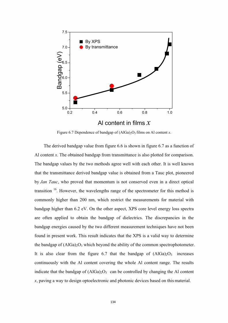
In Chapter 6, bandgap tunable (AlGa)2O3 films were deposited on sapphire
substrates by PLD. The deposited films are of high transmittance as measured by
spectrophotometer. The Al contents in films increase linearly with that of the targets.
The measurement of bandgap energies by examining the onset of inelastic energy loss
in core-level atomic spectra using X-ray photoelectron spectroscopy is proved to be
valid for determining the bandgap of (AlGa)2O3 films as it is in good agreement with
the bandgap values from transmittance spectra. The measured bandgap of (AlGa)2O3
Page 5
IV
films increases continuously with the Al content covering the whole Al content range
from about 5 to 7 eV, indicating PLD is a promising growth technology for growing
bandgap tunable (AlGa)2O3 films.
Page 6
V
Contents
1 Introduction …………………………………………………….………………….1
1.1 Background………………………………………………………..……………1
1.2 Review of studies on Ga2O3, (Ga1-xInx)2O3 and (AlxGa1-x)2O3 films…….…..….2
1.2.1 Ga2O3……..………………………………………….……………….….…2
1.2.2 Si doped Ga2O3………….……………………………………………….…6
1.2.3 (Ga1-xInx)2O3……………………..…………………………………..……..8
1.2.4 (AlxGa1-x)2O3……………………..…………………………..…….……..11
1.3 Purpose and Outline…………………………………………………………...12
References……………………………………………………………………..15
2 Film growth and characterization methods……………………...……………...18
2.1 Film deposition techniques…………………………………………………….18
2.2 Pulsed laser deposition………………………………………………………...20
2.2.1 Basic of pulsed laser deposition………………………………………..…20
2.2.2 The deposition process……………………………………………………22
2.2.3 The pulsed laser deposition equipment used in this research……………..24
2.2.4 The film growth procedures………………………………………………26
2.3 Characterization methods……………………………………………………...28
References……………………………………………………………………..34
3 Growth and characterization of Ga2O3 films……………………………………35
3.1 Introduction……………………………………………………………………35
3.2 Oxygen pressure influence………………………………………………..…...36
3.2.1 Growth rate………………………………………………………………..36
3.2.2 Crystal structure…………………………………………………………..38
3.2.3 Transmittance and surface morphology………………………………......39
Page 7
VI
3.2.4 Discussions………………………………………………………….…….41
3.3 Substrate temperature influence………….……………………………………42
3.3.1 Crystal structure……….………………………………………………….43
3.3.2 Optical properties…....................................................................................48
3.3.3 Surface morphology....................................................................................49
3.3.4 Valence band structure…………………..…………………………..…...53
3.4 Growth time influence…………………………………………………………54
3.5 Annealing effects…………………………………………………….…….…..58
3.5.1 Annealing effect on films deposited at RT………………………….…….59
3.5.2 Annealing effect on films deposited at 500 oC…………………………....63
3.5.3 Annealing effect on CL spectra…………………………………………...66
3.6 Conclusions……………………………………………………………………67
References……………………………………………………………………..69
4 Effect of Si doping on properties of Ga2O3 films…………………………..…....71
4.1 Introductions…………………………………………………………………...71
4.2 Si content influence…………………………………………………………....72
4.3 Substrate temperature influence…………………………………………….....81
4.4 Oxygen pressure influence………….................................................................86
4.5 Conclusions………………………………………………………………..…..89
References……………………………………………………………………..91
5 Growth and characterization of (Ga1-xInx)2O3 films……………...…………….92
5.1 Introduction…………………………………………………………….…..….92
5.2 Bandgap engineering of (Ga1-xInx)2O3 films…………………………………..93
5.2.1 Growth parameters………………………………………………….…….93
5.2.2 Optical properties…...…………………………………………………….94
5.2.3 Structure and surface morphologies……………………………..……..…98
5.3 Thermal annealing impact on crystal quality of (GaIn)2O3 alloys……....…...101
5.4 Toward the understanding of annealing effects on (GaIn)2O3 films…………108
Page 8
VII
5.4.1 Influence of annealing gas ambient…………………………………...…109
5.4.2 Influence of annealing temperature…………………………………...…114
5.5 Annealing effect on films with different indium content…………………….118
5.6 Conclusions…………………………………………………………………..121
References…………………………………………………………….……...124
6 Growth and characterization of (AlGa)2O3 films………………………….…..126
6.1 Introduction…………………………………………………………………..126
6.2 The Al content in the film……………………………………………………127
6.3 Structure of the (AlGa)2O3 films……………………………………………..129
6.4 Transmittance and bandgap of the (AlGa)2O3 films…………………………130
6.5 Conclusions…………………………………………………………………..135
References……………………………………………………………………136
7 Summary……………………………………...………………………………….137
Acknowledgments……………………………………………….…….……………141
List of publications………………………………………………………………….142
Abbreviations……………………………………………………………………….144
Page 9
1
Chapter 1
Introduction
1.1 Background
Oxide semiconductive novel thin films of homo and heterostructures are
technologically attractive for future devices because of their exciting fundamental
intrinsic and extrinsic optical, electrical, magneto-optical, and piezoelectric properties.
They have potential applications such as power device, piezoelectric sensors, thin film
transistors and ultraviolet detectors. Such materials are recognized as being suitable
for extreme environment applications such as high temperatures, intense radiation and
corrosive environments. They can be deposited using conventional process methods
such as sputting, pulsed laser deposition (PLD), metal-organic chemical vapor
deposition (MOCVD) and molecular beam epitaxy (MBE).
Of the oxide semiconductor, Ga2O3 is a potential candidate due to its direct and
wide bandgap and physical and chemical stabilities. For a semiconductor material, it
is important to tail its electronic, magnetic, optical properties through doping, alloying,
quantum wells and heterostructures and nano-engineering, thus one can realize many
technologically important devices like laser diodes, visible and solar blind detectors,
transparent electronic devices, thin film transistors, and spintronic devices. To realize
the tailing of those properties, one of the cores is the bandgap tailing engineering.
Page 10
2
1.2 Review of studies on Ga2O3, (Ga1-xInx)2O3 and (AlxGa1-x)2O3 films
1.2.1 Ga2O3
(1) Properties
It is known that properties of Ga2O3 films depend highly on its structure. For the
phase of Ga2O3, five polymorphs 1: α, β, γ, δ and ε phases, are known so far as shown
in table 1.1. The first α phase with a hexagonal structure is obtained on heating
GaO2H in air about 500 oC. Bohm et al. 2 reported the third form, γ-Ga2O3, similar to
γ-Al2O3, having a unit cell edge of 8.22 Å. δ-Ga2O3, which has analogous structurally
to Mn2O3, In2O3,Ti2O3, etc, corresponds to the body centered, cubic structure of the
rare earths 1. ε-Ga2O3 has been considered to have a crystal structure similar to
κ-Al2O3 in Pna21 space group 3. β-Ga2O3 with a monoclinic structure is commonly
formed under ordinary conditions and is thought to be the most thermodynamically
stable phase. Heat treatment of the other metastable transition phases including α-, γ-,
δ-, and ε-Ga2O3 converts them to β-Ga2O3. The conversion relationships among the
forms are indicated in figure 1.1 1.
Table 1.1 Crystal structures, lattice parameters of Ga2O3 polymorphs.
Phase Space group
Crystal structure
Lattice parameters
Density
(g cm-3)
PDF card
number
α R3c Rhombohedral a=4.98 Å c=13.43 Å α=120o
6.47 PDF#43-1013
β C2/m Monoclinic a=12.23 Å b=3.04 Å c=5.8 Å β=103.7o
5.94 PDF#43-1012
γ Fd-3m Cubic a=8.22 Å 6.05 PDF#20-0426
δ Ia-3 Cubic a=10 Å 5.18 PDF#06-0529
ε Pna21 Orthorhombic a=5.12 Å b=8.79 Å c=9.41 Å
5.88 PDF#06-0509
Page 11
3
Figure 1.1 Conversion relationships among the five polymorphs of Ga2O3.
Yoshioka et al. 3 have investigated the structures and energetics of five Ga2O3
polymorphs using first-principles calculations. The expansivity increases in the order
β, ε, α and δ, and the bulk modulus increases in the order β, ε, δ and α at low
temperatures. The formation energies are in the order β < ε < α < δ < γ at low
temperatures. With the increase of temperature, the difference in free energy between
the ε-phase and β-phase becomes smaller, and vanishes at around 1600 K 3 .
Monoclinic β-Ga2O3, with a melting point of 1740 oC, is the most stable
crystalline structure. The gallium ions are in distorted octahedral and tetrahedral sites,
with Ga-O bond distances of 2.00 and 1.83 Å, respectively, and the oxide ions are in a
distorted cubic closest packing arrangement. These distortions are in fact the reasons
for the great level of stability of β-Ga2O3 4. The octahedral coordination gallium ions
named Ga(VI) and the tetrahedral coordination Ga(IV) are shown in figure 2. As
shown in the figure, the doubly connected straight chains of GaO6 edge shared
octahedra run along b, and the chains are connected by GaO4 tetrahedra chains. On
another aspect, (-201) oriented films in which the b axis is parallel to the substrate is
suggested to enhance the conductivity of β-Ga2O3 film 5-7, because octahedral Ga(VI)
chains which are considered to constitute the paths followed by carrier electrons are
present in the lattice along the b axis, as shown in figure 1.2.
Page 12
4
Figure 1.2 Arrangements of the atoms in β-Ga2O3.
The stability of a material basically includes the ability against high temperatures
and corrosive environments. β-Ga2O3 substrate is reported to be chemically stable
against both acids and alkalis except HF and NaOH. Aqueous HF solution can be used
to etch β-Ga2O3 uniformly at room temperature 8.The β-Ga2O3 surface was found to
decompose above 1150 oC in N2, while at only 350 °C in the presence of H2 9. These
properties promise the application of β-Ga2O3 based devices under most of the
extreme environments, while reserving the door for the fabricating of those devices
utilizing existing technology such as etching, lithography etc.
(2) Growth method of Ga2O3 thin film
One of the merit of β-Ga2O3 compared with other wide bandgap materials such
as SiC, GaN, AlN and diamond is that large-diameter, high-quality single-crystal
substrates can be fabricated by melt growth methods, such as edge-defined film-fed
growth (EFG) 10, Czochralski 11 and floating zone 12-14 methods. Two inch diameter
β-Ga2O3 wafers with low dislocation densities on the order of 104 cm-2 fabricated by
EFG are now available 15 .
One of the key to the fabrication of β-Ga2O3 based devices such as chips can be
Ga (IV)
Ga (VI)
b
Page 13
5
regarded as the deposition technology, since the microelectronic solid-state devices
are almost based on material structures created by thin film deposition. Several
physical and chemical techniques have been employed to deposit β-Ga2O3 films such
as sputtering 16-18, chemical vapor deposition 19, 20, spray pyrolysis 21, sol-gel method
22, thermal evaporation 23, 24, molecular beam epitaxy 25-27, and pulsed laser deposition
7, 28-30. Recently, thick β-Ga2O3 films grown by halide vapor phase epitaxy (HVPE)
were also reported 31, 32. Because of the different growth mechanism of each method,
the substrate temperature for the growth of crystalline β-Ga2O3 is also different. Table
1.2 lists some growth methods of β-Ga2O3 films and the corresponding crystallization
temperature. As shown in that table, the deposition methods of MOCVD, MBE and
PLD show the lowest crystallization temperature around 400~500 oC.
Table 1.2 Growth methods of β-Ga2O3 films and the crystallization temperatures.
Growth techniques Substrates Crystalline temperature
HVPE31 β-Ga2O3 800-1050 oC
HVPE32 sapphire 1050 oC
thermal evaporation23 glass post annealing at 600 oC
evaporation in oxygen plasma24 sapphire 800 oC
Sol-Gel22 sapphire 600 oC
MOCVD19 sapphire 500 oC
sputtering18 Si (111) post annealing at 700 oC
MBE27 β-Ga2O3 560 oC
plasma-assisted MBE25 sapphire 500 oC
PLD29 sapphire 500 oC
PLD7 sapphire 380 oC
PLD30 sapphire 700~ 800 oC
(3) Research progress of Ga2O3 thin film grown by PLD
Some growth of Ga2O3 films by PLD has been reported recently. Orita et al. 33
Page 14
6
have investigated the conductivity of Ga2O3 films by Sn doping using pulsed-laser
deposition method. They at first tried to deposit Sn-doped β-Ga2O3 on silica glass.
N-type conductivity up to 1 S cm-1 was obtained under low O2 partial pressure (10-5
Pa) at substrate temperatures above 800 oC 33. Two years later, they 7 reported an
increased conductivity of 8.2 S cm-1, which was obtained at a low deposition
temperature of 380 oC using sapphire substrate. However, the crystal structures of the
films easily changed from β to ε phase when the substrate temperature is above 435
oC 7. Sn doping effect on Ga2O3 films grown by PLD was also reported by Matsuzaki
et al. 29, 34. They found that Sn-doped Ga2O3 grown on yttria-stabilized zirconia (111)
with post-annealing at 1400 oC did not exhibit detectable electrical conduction. Films
with electrical conductivities applicable to FETs were obtained at substrate
temperature between 500 to 550 oC and oxygen pressure from 5×10⁻⁴ Pa to 1×10⁻³ Pa
on sapphire substrates. However, the structure was determined to be orthorhombic
with large possibility of a higher-symmetry hexagonal or rhombohedral system 29, 34.
Both researches by Orita and Matsuzaki indicated that Sn doping can increase the
conductivity of Ga2O3 films but easily leads to a non-stable phase.
Hayashi et al. 35 have investigated the Mn doping effect on Ga2O3 films. They
found that Mn-doped film grown on sapphire substrate at 500 oC shows γ phase with
spinel structure. Mn atoms are located at tetrahedrally coordinated Ga sites with a
valence of +2. The doped sample shows ferromagnetism up to 350 K. They also
demonstrated the fabrication of single domain Mn-doped γ-Ga2O3 films with a
defective spinel structure on spinel substrates by PLD at 500 oC 28.
Lee et al. 36 have utilized another kind of substrate, GaN, to deposit Ga2O3 films
by PLD. (-201) oriented β-Ga2O3 thin films were obtained at substrate temperature of
800 °C and the dielectric constant were about 13.9. The β-Ga2O3/GaN structure
showed sharp interface comparing with thermally oxidized β-Ga2O3/GaN film.
1.2.2 Si doped Ga2O3
It is well known that the pure Ga2O3 is an insulator 12. As for semiconductor
devices, suitable amount of carrier density is indispensable. For example, the typical
Page 15
7
carrier density (Si based devices) is 1016 cm-3 for the channel of
metal-oxide-semiconductor field-effect transistor (MOSFET); 1019, 1017, and 1015
cm-3 for the emitter, base and collector of bipolar transistor, respectively 37. Thus
selecting the appropriate doping elements to improve the carrier density of Ga2O3 is
very important. It is well known that Sn and Si are efficient n type dopants for bulk
β-Ga2O3. Orita et al. 33 have obtained Ga2O3 films with n type conductivity up to 1
Scm-1 by Sn doping at substrate temperatures above 800 oC. And the conductivity can
be improved to 8.2 Scm-1 by optimizing the deposition conditions 7.On the other hand,
Varley et al. 38 have theoretically studied donor impurities in β-Ga2O3 based on the
density functional theory and suggested that Si is an efficient n type dopant. Actually,
the effect of Si doping on the carrier density for β-Ga2O3 bulk single crystals was
proved experimentally. Villora et al. 39 showed that the carrier density of bulk
β-Ga2O3 can be intentionally controlled over three orders of magnitude from 1016 to
1018 cm-3 by Si doping. Sasaki et al. 40 developed a donor doping technique for
β-Ga2O3 substrate by using Si-ion (Si+) implantation with followed high temperature
thermal annealing, the carrier density is reported to be 1019 cm-3. Thus, the
conductivity control of β-Ga2O3 bulk single crystal has been established well.
However, for β-Ga2O3 thin films, the intentional control of the electrical properties
is still a remaining issue. Gogova et al. 41 have grown Si-doped β-Ga2O3 films by
metal organic vapor phase epitaxy (MOVPE). Although secondary ion mass
spectrometry showed that Si was incorporated in the films, Hall effect measurements
demonstrated that the resulting material was not electrically conductive. Takakura et
al. 42 also found that the conductivity does not increase by Si doping for β-Ga2O3
films grown by RF magnetron sputtering. Müller et al. 43 have tried to grow Si-doped
β-Ga2O3 thin films by PLD and obtained Ga2O3 film with conductivity of 0.2 S cm-1.
Unfortunately, they did not report on carrier density and optical properties of these
films. 4
Page 16
8
1.2.3 (Ga1-xInx)2O3
(1) Properties
In-Ga-Al-O system is a promising system for semiconductor device applications
in the ultraviolet (UV) wavelength region as its possible tunable bandgap 3.5 (In2O3)
~ 4.9 (Ga2O3) ~ 8.6 eV (Al2O3) which covers the wavelength from 144 to 354 nm. As
the UV spectrum is usually divided into four regions which includes vacuum UV
(10-200 nm, UV-V), short wave UV (200-280 nm, UV-C), middle wave UV (280-315
nm, UV-B) and long wave UV (315-400 nm, UV-A), it is clear that the In-Ga-Al-O
system almost covers the whole range of the UV spectrum, thus it is a very promising
candidate for the UV device applications. It has promising usages such as (1)
destruction of microorganisms for air/water purification (240-280 nm), (2) UV-
identification , label tracking, bar coding (230-365 nm), (3) optical sensors and
analytical instrumentation (230-400 nm), (4) forensic analysis, drug detection
(250-300 nm), (5) protein analysis, DNA sequencing, drug discovery (270-300 nm),
(6) medical imaging of cells (280-400 nm), (7) solid-state lighting (300-400 nm) , (8)
curing of polymers and printer inks (300-365 nm) and (9) light therapy in medicine
(300-320 nm).
For the complex (Ga1-xInx)2O3 alloy, the component oxides Ga2O3 and In2O3 have
different crystal structure. The cubic In2O3 (bixbyite) is stable from room temperature
to the melting point. This body-centered cubic structure has 16 In2O3 per unit cell and
a cell dimension of 10.117 Å. The stable monoclinic β-Ga2O3 has four Ga2O3 per unit
cell. Half of the cation sites are octahedral coordinated and the other half are
tetrahedrally coordinated as already described. The alloyed (Ga1-xInx)2O3 can either be
of monoclinic or cubic structure or the mixture, depending on the cation composition
of the alloy.
A band structure calculation of β-Ga2O3 showed that the conduction band is
anisotropic and exclusively constituted by the antibonding states of the Ga–O bonds
in octahedral sites, with a major contribution arising from the 4s-AOs (atomic
orbitals ) of Ga ions 6. From X-ray diffraction 44 and the study of the hyperfine
Page 17
9
interaction of Cd in In-doped β-Ga2O3 45, it was proved that In ions occupy
preferentially the octahedral sites. Thus, owing to the preference of In ions for
octahedral sites, a significant contribution of In-AOs to the conduction band edge can
be expected. And Binet et al. have demonstrated the participation of In orbitals in the
conduction band edge 46. And because of the above features, the bandgap engineering
of monoclinic structured (Ga1-xInx)2O3 solid state seems easy to realize. However, the
bandgap engineering of cubic structured (Ga1-xInx)2O3 solid solution becomes difficult
because very small amount of Ga can be incorporated into the cubic In2O3 44.
(2) Research progress
The research on (Ga1-xInx)2O3 alloy was began in 1997 by Doreen D. Edwards et al.
44. They reported that the solubility limit of In2O3 in the β-gallia structure decreases
with increasing temperature from 44.1 mol% at 1000 °C to 41.4 mol% at 1400 °C.
The solubility limit of Ga2O3 in cubic In2O3 increases with temperature from 4 mol%
at 1000 °C to 10.0 mol% at 1400 °C 44.
Before 2001, research of this system was focused on the bulk solid solution and
mainly the solubility of (Ga1-xInx)2O3 system. Binet et al. 46 reported that the samples
(Ga1-xInx)2O3 elaborated by coprecipitation and treated at 1400 oC show the β-gallia
phase for x<0.4. Optical spectroscopies show a decrease of the bandgap when x
increases. Patzke et al. 47 found β-(Ga1-xInx)2O3 with a maximum In2O3-content of 48
mol% and cubic (Ga1-xInx)2O3 with less than 10 mol% Ga2O3 can be obtained. Ratko
et al. 48 reported that the solubility of Ga2O3 in In2O3 cubic lattice has a limit up to
15-16.5 mol%. Vigreux et al. 49 investigated solid solutions of β-(Ga1-xInx)2O3 (x≤0.4)
with β-gallia structure by Raman spectroscopy. A continuous evolution with a linear
shift of the Raman lines with increasing x was observed in the existence range of the
solid solution (x≤0.4). For 0.4≤x≤0.5, strong alterations of the Raman spectra were
observed, corresponding either to the demixing of the solid solutions for the samples
elaborated at 1400 oC or to the occurrence of a new phase with γ-alumina structure for
samples elaborated at 1550 oC 49. From the above results, the solubility above 1000 oC
was proved to be less than 45 mol% for In2O3 in monoclinic Ga2O3 and 10 mol% for
Page 18
10
Ga2O3 in cubic In2O3.
From 2002 to 2010, research on nanowires, films of (Ga1-xInx)2O3 appeared. But
the number of reports was also small and the reports were focused on electrical
properties.
Wang et al. 50 reported that (GaxIn1−x)2O3, where x=0.0~0.55, with a
homogeneously Ga-substituted, cubic In2O3 microstructure was grown by MOCVD.
The lowest electrical resistivities were found in films deposited on quartz at 500 °C
with Ga/(In + Ga) atomic ratios near 0.06. They concluded that the major determinant
of carrier scattering is not high-angle grain boundaries or lattice distortions but rather
the presence of neutral or ionized impurity scattering centers.
Lim et al. 51 reported that gallium-doped indium oxide use as highly transparent
and low resistance ohmic contacts to p-GaN. The contact annealed at 600 °C for 1
min in a nitrogen ambient showed a low specific contact resistance and high light
transmittance.
Oshima et al. 52 reported (Ga1-xInx)2O3 alloy thin films grown on c-plane sapphire
substrates with a thin Ga2O3 buffer layer by MBE. Apparent phase separation and In
segregation was observed even at x=0.08 when grown at high temperatures of 700 or
800 oC. In order to suppress the phase separation, low temperature growth at 600 ℃
or lower was found to be essential and effective.
Su et al. 53 investigated In-doped Ga2O3 zigzag-shaped nanowires and undoped
Ga2O3 nanowires synthesized by vapor–solid (VS) growth mechanism. Compared
with undoped Ga2O3 nanowires, the shapes of the as-synthesized In-doped Ga2O3
nanowires have changed obviously.
After 2011, the researches on this system become prosperous, especially for
nano-wires. Thin films growth by sol-gel method, CVD, and MBE have also been
reported.
Kokubun et al. 54 prepared (Ga1-xInx)2O3 thin films at 900 oC using a sol–gel
method, on (0001) sapphire substrates. For In content below 0.4, films are of single
phase with the same monoclinic structure as β-Ga2O3. For films with x>0.8 cubic
In2O3 solid solution structure exhibited. Between In content 0.4 and 0.8, both phases
Page 19
11
exist but with poor transmittance. Knapp et al. 55 used Aerosol-Assisted Chemical
Vapor Deposition (AACVD) reaction and post annealing at 1000 oC to obtain a
Ga-substituted cubic In2O3 structure (Ga0.6In1.4O3.1). They also considered that for the
growth of (Ga1-xInx)2O3 films with high Ga content, the crystallization temperature is
high. Typically deposition of β-Ga2O3 below 650 oC often results in amorphous oxide
56.
Farvid et al. 57 investigated (Ga1-xInx)2O3 nano crystals at low temperature (<250
oC). For In content below 13%, the nano crystals exhibit γ-Ga2O3 structure while for
In content above 47%, exhibits corundum-type In2O3 structure. In3+ occupies only
octahedral, rather than tetrahedral, sites in the spinel-type γ-Ga2O3 nanocrystal host
lattice. Lin et al. 58 investigated tunable growth of In-doped Ga2O3 (Ga2O3:In) and
Ga-doped In2O3 (In2O3:Ga) nanowires (NWs) on Au-coated Si substrates by
modulating the amount of water vapor in flowing Ar at 700–750 oC. In Ar only the
Ga2O3:In NWs were grown, while in wet Ar the In2O3:Ga NWs were synthesized
instead. López et al. 59 found that indium plays a major role in the observed
morphologies of the nano structures.
1.2.4 (AlxGa1-x)2O3
Because of the similar electron structures of Al and Ga, Al can alloy with
Ga2O3 to form (AlxGa1-x)2O3 alloy. (AlxGa1-x)2O3 has a tunable larger bandgap than
Ga2O3 because Al2O3 has a big bandgap (~8.8 eV for bulk material, ~6.4 eV for
amorphous Al2O3 films).
The investigation of Ga-Al-O system is mainly focused on the formation of
γ-Al2O3-Ga2O3 by means of hydrothermal to serve as catalyst. Zahir et al. has
reported Ga2O3 as dopants to mesoporous γ-Al2O3 membrane 60. Watanabe et al.
synthesized γ-Ga2O3–Al2O3 solid solutions by several methods 61, 62.
The reports on the growth of (AlxGa1-x)2O3 films by vacuum techniques appeared
only in recent years and the number is still seldom. Oshima et al. 63 has successfully
grown β-(AlxGa1-x)2O3 on (100)-oriented β-Ga2O3 single-crystal substrates by plasma
assisted MBE. The films were grown almost coherently and maintained the β-phase
Page 20
12
up to an Al content of x=0.61. Below an Al content of about x=0.4, step-flow growth
was achieved. Ito et al. 64 have realized corundum structured α-(AlxGa1-x)2O3 thin
films on sapphire by spray-assisted mist chemical vapor deposition. However, the
bandgap engineering on that system was not investigated in detail, which is believed
due to the limitation of the spectrometer wavelength range of the optical method
(commonly longer than 200 nm, which restrict the measurements for material with
bandgap higher than 6.2 eV).
Recent researches revealed that the measurement of bandgap energies by
examining the onset of inelastic energy loss in core-level atomic spectra using X-ray
photoelectron spectroscopy (XPS) is an efficient way to measure the bandgap of wide
bandgap materials 65-68. And that method has driven the bandgap engineering of
(AlxGa1-x)2O3 to go forward. The inelastic collisions include exciting the plasmon in
the bulk and at surface (a fast-moving charged particle can lose energy in the bulk
material to collective high-frequency plasma oscillations of electrons in the valence
band) and single-particle excitations due to band-to-band transitions 68. The onset of
the inelastic energy loss spectra equal to the bandgap energy because the fundamental
lower limit of inelastic loss is the bandgap energy 69.
1.3 Purpose and Outline
As has discussed above, Ga2O3 is a material that has a high dielectric constant,
good thermal stability, and superior performance as a wide-bandgap semiconductor
material. It has potential applications such as power device, piezoelectric sensors, thin
film transistors and ultraviolet detectors. And it is also suitable for extreme
environment applications such as high temperatures, intense radiation and corrosive
environments. However, the growth of Ga2O3 by PLD is still in its infancy. The
researches of Ga2O3 films grown by PLD mainly aimed to change its electrical and
magnetic properties. Specifically, to reach those goals, impurities such as Sn and Mn
have to be incorporated into the films, which often result in a non-stable structure.
The detailed investigation of substrate temperature and oxygen influence on the
Page 21
13
structure and properties of non-doped Ga2O3 deposited by PLD is thus highly desired.
On another aspect, for a semiconductor material, it is important to tail its
electronic, magnetic, and optical properties through doping, alloying, quantum wells
and heterostructures, and nano-engineering thus one can realize many technologically
important devices like laser diodes, visible and solar blind detectors, transparent
electronic devices, thin film transistors, and spintronic devices. To realize the tailing
of those properties, one of the cores is the bandgap tailing engineering. In and Al can
alloy with Ga2O3 to form (Ga1-xInx)2O3 and (AlxGa1-x)2O3 alloys to realize the bandgap
engineering because they all belong to the same element group and have similar
electron structures. However, for (Ga1-xInx)2O3 alloy, the bandgap reported is only
restricted in the region of indium content lower than 0.35. Bandgap engineering of
(Ga1-xInx)2O3 films with In content in the whole range is desired. And the bandgap
engineering on (AlxGa1-x)2O3 system is also not investigated in detail, which is
believed due to the limitation of the spectrometer wavelength range of the optical
method (commonly longer than 200 nm, which restricts the measurements for
material with bandgap higher than 6.2 eV).
The purpose of this dissertation mainly includes:
(1) Investigation of growth parameter influence on the structure and properties
of non-doped Ga2O3 deposited by PLD.
(2) Control of the conductivity of Ga2O3 film by Si doping.
(3) Bandgap engineering of (Ga1-xInx)2O3 films with In content in the whole
range.
(4) Bandgap engineering of (AlxGa1-x)2O3 films with Al content in the whole
range.
This dissertation is divided into seven chapters, and the outline is as follows.
In Chapter 1, the background and the purpose of this study are presented.
In Chapter 2, the film growth and characterization methods are introduced. In Chapter 3, the influence of oxygen pressure, substrate temperature, deposition
time on the structure and optical properties of Ga2O3 films grown by PLD is described.
The influence of post annealing is also been discussed.
Page 22
14
In Chapter 4, the effect of Si doping on the properties of Ga2O3 films grown by
PLD is described. The properties of films deposited with different Si content and Si
doped films grown under different growth conditions are discussed in detail.
In Chapter 5, the growth of crystalline and bandgap tunable (Ga1-xInx)2O3 films
on sapphire (0001) substrate is described. The elimination of the phase separation was
discussed in detail.
In Chapter 6, bandgap tunable (AlGa)2O3 films are deposited on sapphire
substrates by PLD. The measurement of bandgap energies by examining the onset of
inelastic energy loss in core-level atomic spectra using X-ray photoelectron
spectroscopy is discussed.
In Chapter 7, the summary of this study is described.
Page 23
15
References:
1. R. Roy, V. G. Hill and E. F. Osborn, J. Am. Chem. Soc., 1952, 74 719.
2. J. Bohm, Angew. Chem., 1940, 53, 131.
3. S. Yoshioka, H. Hayashi, A. Kuwabara, F. Oba, K. Matsunaga and I. Tanaka, Journal of Physics:
Condensed Matter, 2007, 19, 346211.
4. E. Baker and R. King, Wiley: Chichester, 1994.
5. N. Ueda, H. Hosono, R. Waseda and H. Kawazoe, Appl. Phys. Lett., 1997, 71, 933.
6. L. Binet, D. Gourier and C. Minot, J. Solid State Chem., 1994, 113, 420.
7. M. Orita, H. Hiramatsu, H. Ohta, M. Hirano and H. Hosono, Thin Solid Films, 2002, 411, 134.
8. S. Ohira and N. Arai, physica status solidi (c), 2008, 5, 3116.
9. R. Togashi, K. Nomura, C. Eguchi, T. Fukizawa, K. Goto, Q. T. Thieu, H. Murakami, Y.
Kumagai, A. Kuramata, S. Yamakoshi, B. Monemar and A. Koukitu, Jpn. J. Appl. Phys., 2015,
54, 041102.
10. H. Aida, K. Nishiguchi, H. Takeda, N. Aota, K. Sunakawa and Y. Yaguchi, Jpn. J. Appl. Phys.,
2008, 47, 8506.
11. Y. Tomm, P. Reiche, D. Klimm and T. Fukuda, J. Cryst. Growth, 2000, 220, 510.
12. N. Ueda, H. Hosono, R. Waseda and H. Kawazoe, Appl. Phys. Lett., 1997, 70, 3561.
13. E. G. Víllora, K. Shimamura, Y. Yoshikawa, T. Ujiie and K. Aoki, Appl. Phys. Lett., 2008, 92,
202120.
14. Y. Tomm, J. M. Ko, A. Yoshikawa and T. Fukuda, Sol. Energ. Mat. Sol. C., 2001, 66, 369.
15. M. Higashiwaki, K. Sasaki, A. Kuramata, T. Masui and S. Yamakoshi, physica status solidi (a),
2014, 211, 21.
16. M. Fleischer, W. Hanrieder and H. Meixner, Thin Solid Films, 1990, 190, 93.
17. L. Jianjun, Y. Jinliang, S. Liang and L. Ting, Journal of Semiconductors, 2010, 31, 103001.
18. Y. Zhang, J. Yan, Q. Li, C. Qu, L. Zhang and T. Li, Physica B: Condensed Matter, 2011, 406,
3079.
19. C.-Y. Huang, R.-H. Horng, D.-S. Wuu, L.-W. Tu and H.-S. Kao, Appl. Phys. Lett., 2013, 102,
011119.
20. D. Shinohara and S. Fujita, Jpn. J. Appl. Phys., 2008, 47, 7311.
21. A. Ortiz, J. C. Alonso, E. Andrade and C. Urbiola, J. Electrochem. Soc., 2001, 148, F26.
22. Y. Kokubun, K. Miura, F. Endo and S. Nakagomi, Appl. Phys. Lett., 2007, 90, 031912.
23. A. A. Dakhel and W. E. Alnaser, Microelectron. Reliab, 2013, 53, 676.
24. S. Nakagomi and Y. Kokubun, J. Cryst. Growth, 2012, 349, 12.
25. T. Oshima, T. Okuno and S. Fujita, Jpn. J. Appl. Phys., 2007, 46, 7217.
26. T. Oshima, T. Okuno, N. Arai, N. Suzuki, S. Ohira and S. Fujita, Applied Physics Express, 2008,
1, 011202.
27. M. Higashiwaki, K. Sasaki, T. Kamimura, M. Hoi Wong, D. Krishnamurthy, A. Kuramata, T.
Masui and S. Yamakoshi, Appl. Phys. Lett., 2013, 103, 123511.
28. H. Hayashi, R. Huang, F. Oba, T. Hirayama and I. Tanaka, J. Mater. Res., 2011, 26, 578.
29. K. Matsuzaki, H. Hiramatsu, K. Nomura, H. Yanagi, T. Kamiya, M. Hirano and H. Hosono,
Thin Solid Films, 2006, 496, 37.
30. A. Goyal, B. S. Yadav, O. P. Thakur, A. K. Kapoor and R. Muralidharan, J. Alloy. Compd.,
2014, 583, 214.
31. H. Murakami, K. Nomura, K. Goto, K. Sasaki, K. Kawara, Q. T. Thieu, R. Togashi, Y. Kumagai,
Page 24
16
M. Higashiwaki, A. Kuramata, S. Yamakoshi, B. Monemar and A. Koukitu, Applied Physics
Express, 2015, 8, 015503.
32. Y. Oshima, E. G. Vίllora and K. Shimamura, J. Cryst. Growth, 2015, 410, 53.
33. M. Orita, H. Ohta, M. Hirano and H. Hosono, Appl. Phys. Lett., 2000, 77, 4166.
34. K. Matsuzaki, H. Yanagi, T. Kamiya, H. Hiramatsu, K. Nomura, M. Hirano and H. Hosono,
Appl. Phys. Lett., 2006, 88, 092106.
35. H. Hayashi, R. Huang, H. Ikeno, F. Oba, S. Yoshioka, I. Tanaka and S. Sonoda, Appl. Phys.
Lett., 2006, 89, 181903.
36. S.-A. Lee, J.-Y. Hwang, J.-P. Kim, S.-Y. Jeong and C.-R. Cho, Appl. Phys. Lett., 2006, 89,
182906.
37. S. M. Sze and K. K. Ng, Physics of semiconductor devices, John Wiley & Sons, 2006.
38. J. B. Varley, J. R. Weber, A. Janotti and C. G. Van de Walle, Appl. Phys. Lett., 2010, 97,
142106.
39. E. G. Víllora, K. Shimamura, Y. Yoshikawa, T. Ujiie and K. Aoki, Appl. Phys. Lett., 2008, 92,
202120.
40. K. Sasaki, M. Higashiwaki, A. Kuramata, T. Masui and S. Yamakoshi, Applied Physics Express,
2013, 6, 086502.
41. D. Gogova, G. Wagner, M. Baldini, M. Schmidbauer, K. Irmscher, R. Schewski, Z. Galazka, M.
Albrecht and R. Fornari, J. Cryst. Growth, 2014, 401, 665.
42. K. Takakura, S. Funasaki, I. Tsunoda, H. Ohyama, D. Takeuchi, T. Nakashima, M. Shibuya, K.
Murakami, E. Simoen and C. Claeys, Physica B: Condensed Matter, 2012, 407, 2900.
43. S. Müller, H. von Wenckstern, D. Splith, F. Schmidt and M. Grundmann, physica status solidi
(a), 2014, 211, 34.
44. D. D. Edwards, P. E. Folkins and T. Mason, J.Am.Ceram.Soc, 1997, 80, 253.
45. A. F. Pasquevich, M. Uhrmacher, L. Ziegeler and K. P. Lieb, Phys. Rev. B, 1993, 48, 10052.
46. L. Binet, G. Gauthier, C. Vigreux and D. Gourier, J. Phys. Chem. Solids, 1999, 60, 1755.
47. G. Patzke and M. Binnewies, Solid State Sci., 2000, 2, 689.
48. A. Ratko, O. Babushkin, A. Baran and S. Baranc, J. Eur. Ceram. Soc., 1998, 18, 2227.
49. C. Vigreux, L. Binet, D. Gourier and B. Piriou, J. Solid State Chem., 2001, 157, 94.
50. A. Wang, N. L. Edleman, J. R. Babcock and T. J. Marksa, J. Mater. Res., 2002, 17, 3155.
51. J.-H. Lim, E.-J. Yang, D.-K. Hwang, J.-H. Yang, J.-Y. Oh and S.-J. Park, Appl. Phys. Lett.,
2005, 87, 042109.
52. T. Oshima and S. Fujita, physica status solidi (c), 2008, 5, 3113.
53. Y. Su, M. Gao, X. Meng, Y. Chen, Q. Zhou, L. Li and Y. Feng, J. Phys. Chem. Solids, 2009, 70,
1062.
54. Y. Kokubun, T. Abe and S. Nakagomi, physica status solidi (a), 2010, 207, 1741.
55. C. E. Knapp, G. Hyett, I. P. Parkin and C. J. Carmalt, Chem. Mater., 2011, 23, 1719.
56. C. E. Knapp, A. Kafizas, I. P. Parkin and C. J. Carmalt, J. Mater. Chem., 2011, 21, 12644.
57. S. S. Farvid, T. Wang and P. V. Radovanovic, J. Am. Chem. Soc., 2011, 133, 6711.
58. W.-T. Lin, C.-Y. Ho, Y.-M. Wang, K.-H. Wu and W.-Y. Chou, J. Phys. Chem. Solids, 2012, 73,
948.
59. I. López, A. D. Utrilla, E. Nogales, B. Méndez, J. Piqueras, A. Peche, J. Ramírez-Castellanos
and J. M. González-Calbet, The Journal of Physical Chemistry C, 2012, 116, 3935.
60. M. H. Zahir, K. Sato, H. Mori, Y. Iwamoto, M. Nomura and S.-i. Nakao, J. Am. Ceram. Soc.,
Page 25
17
2006, 89, 2874.
61. T. Watanabe, T. Masuda, Y. Miki, Y. Miyahara, H.-J. Jeon, S. Hosokawa, H. Kanai, H. Deguchi
and M. Inoue, J. Am. Ceram. Soc., 2010, 93, 3908.
62. T. Watanabe, Y. Miki, T. Masuda, H. Deguchi, H. Kanai, S. Hosokawa, K. Wada and M. Inoue,
Ceram. Int., 2011, 37, 3183.
63. T. Oshima, T. Okuno, N. Arai, Y. Kobayashi and S. Fujita, Jpn. J. Appl. Phys., 2009, 48,
070202.
64. H. Ito, K. Kaneko and S. Fujita, Jpn. J. Appl. Phys., 2012, 51, 100207.
65. Y. Hori, C. Mizue and T. Hashizume, Jpn. J. Appl. Phys., 2010, 49, 080201.
66. T. Kamimura, K. Sasaki, M. Hoi Wong, D. Krishnamurthy, A. Kuramata, T. Masui, S.
Yamakoshi and M. Higashiwaki, Appl. Phys. Lett., 2014, 104.
67. C. M. Tanner, Y.-C. Perng, C. Frewin, S. E. Saddow and J. P. Chang, Appl. Phys. Lett., 2007,
91, 203510.
68. M. T. Nichols, W. Li, D. Pei, G. A. Antonelli, Q. Lin, S. Banna, Y. Nishi and J. L. Shohet, J.
Appl. Phys., 2014, 115, 094105.
69. F. G. Bell and L. Ley, Phys. Rev. B, 1988, 37, 8383.
Page 26
18
Chapter 2
Film growth and characterization methods
2.1 Film deposition techniques
One of the key to the fabrication of β-Ga2O3 based devices can be regarded as
the deposition technology, since the microelectronic solid-state devices are almost
based on material structures created by thin film deposition. Several physical and
chemical techniques have been employed to deposit β-Ga2O3 films such as sputtering
1-3, chemical vapor deposition 4, 5, spray pyrolysis 6, sol-gel method 7, thermal
evaporation 8, 9, MBE 10-12, and PLD 13-16.
In the following, the commonly used techniques are briefly described. Since in
this work, PLD was exclusively used for the deposition of oxide thin films, this
method is described in more detail in a separated section.
(1) Sol-gel method
The sol-gel process is a colloidal processing route used for the fabrication of
both glassy and ceramic materials. In this process, the sol (or solution) evolves
gradually towards the formation of a gel-like network which contains both liquid
phase and solid phase. Metal alkoxides and metal chlorides are typical precursors,
which undergo hydrolysis and poly condensation reactions to form a colloid.
Colloidal behavior was governed by the interactions between dispersed particles
within the suspending medium. The basic structure or morphology of the solid phase
can range anywhere from discrete colloidal particles to continuous chain-like polymer
networks 17.
The deposition of thin films on solid substrate by sol-gel coatings generally
includes the following steps: (a) preparation of the sol, (b) inducing the sol to change
Page 27
19
into a gel by polycondensation, (c) deposit the gel on substrate, (d) sintering the
shaped gel to desired material by drying and heating the coated layer on substrate.
The advantages of the sol-gel method mainly include: It is a simple, economic
and effective method to produce high quality coatings; it can easily shape materials
into complex geometries in a gel state; composition can be highly controllable.
Despite its advantages, sol-gel technique has some limitations, e.g. weak bonding, low
wear-resistance, high permeability, and difficult controlling of porosity.
(2) MOCVD
MOCVD is a chemical vapour deposition method used to produce thin films in a
substrate. The gases are injected into a reactor. The reaction of organic compounds or
metal organics and hydrides to form crystalline films takes place at the surface of the
substrate.
For example, indium phosphide could be grown in a reactor on a heated substrate.
The first step is to introduce trimethyl indium ((CH3)3In) and phosphine (PH3) into the
reactor. The heated organic precursor molecules will be pyrolyzed. Pyrolysis leaves
the atoms on the substrate surface in the second step. These atoms will bond to the
substrate surface or act with each other thus a new crystalline layer will form in the
last step.
The advantage of this method includes the ability to grow uniform layers, high
purity and potential for large scale commercial applications. The major limitation of
this method is the availability of suitable precursor material. And another limitation is
the use of large quantities of poisonous gases.
(3) Sputtering
A well-known of the glow discharge processes is sputtering. It ejects surface
atoms from an electrode surface (target) by momentum transfer from bombarding ions
to surface atoms 18. Since sputtering produces a vapor of target material, it is similar
to evaporative deposition. The target is bombarded by ionized atoms (mostly argon
atoms). If the energy transferred to the surface atom is three times than the surface
Page 28
20
binding energy, the surface atoms will be sputtered. And a secondary electron is
released from the target material. A magnetic field can be used in the sputtering
processes in order to trap the secondary electrons, thus the ionization of the plasma
near the target can be enhanced 19. The advantages of the sputtering include better step
coverage, easier to deposit alloys and etc. The disadvantage is that some plasma
damage including implanted argon is easy produced.
(4) MBE
MBE is one of several methods to grow single-crystal epitaxial films. It was
invented in the late 1960’s at Bell Telephone Laboratories by J. R. Arthur and Alfred Y.
Cho 20. MBE takes place in high vacuum (~10-8 Pa). The sources for evaporation are
placed in separate Knudsen effusion source cells (deep crucibles in furnaces with
cooled shrouds). The films are deposited on substrates by evaporating the elemental
or molecular constituents of the film evaporated from the sources. The substrates are
held at a temperature appropriate for chemical reaction, epitaxy, and re-evaporation of
excess reactants. Fast shutters are often interposed between the sources and the
substrates for the convenience of growing superlattices.
MBE exhibits many advantages over similar thin film deposition processes,
like vapour deposition such as: significantly improved purity, arbitrarily sharp
deposition resolution, and operation at low temperatures. The limitations of that
method mainly include the complex operation and the expensive equipment.
2.2 Pulsed laser deposition
2.2.1 Basic of pulsed laser deposition
PLD is a physical vapor deposition process which is carried out under a vacuum
system. It has some process characteristics similar with MBE and some with sputter
deposition. A schematical diagram of the PLD system is shown in figure 2.1. A
pulsed laser is excited from a KrF excimer laser source with wavelength 248 nm. The
pulsed laser is focused onto a target of the material to be deposited. The target
Page 29
21
material will be vaporized or ablated by each of the laser pulse if it has sufficiently
high laser energy density, and thus create a plasma plume. The ablated material will
transfer forward until it reaches the surface of the substrate and provides materials
flux for the deposition of film.
Figure 2.1 Schematic diagram of the PLD equipment.
PLD process has some features which make it suitable for complex material film
deposition. The first one is that the stoichiometric transfer of material from the target
to film is possible, because that the high laser energy is absorbed by a small volume
of target material, which makes the ablation process a non-equilibrium one. The
second feature is that background gas can be used to react with the ablated captions.
Especially, the background pressure can be adjusted from ultrahigh vacuum to several
Pa. The third feature is that multicomponent films can be deposited with PLD using
single, stoichiometric targets of the material of interest, or with multiple targets for
each element. Especially, by using programmable multiple targets rotation system, the
growth of complex multi-layers such as quantum well becomes feasible.
Page 30
22
2.2.2 The deposition process
The PLD deposition process can be roughly divided into three main stages. I) the
interaction of the pulsed laser with the target; II) the expansion and the propagation of
plume/ablated plasma; III) thin film growth.
(1) The interaction of the pulsed laser with the target
When the pulsed high-energetic laser beam is focused on a target, the material
will be ablated. At beginning a dense layer of vapor is formed in front of the target.
When the vapor absorbs the reminder energy of the laser, the pressure and
temperature of this vapor will increase and it will be ionized. Because the pressure of
this layer is high, it will expand from the surface of the target and form the so-called
plasma plume. In the duration of expansion, the thermal and the ionization energies
will convert into kinetic energy of the ablated plume with the order of hundreds eV.
Several parameters such as the absorption coefficient and reflectivity of the
target material, the duration of the pulse τ, wavelength λ and frequency of the laser
influence the interaction of the pulsed laser with the target
(2) The expansion and the propagation of plume
At early stage, the shape of the vapor plasma is known to be a cloud which is
strongly forwarded in the direction normal to the surface of the ablated target. Once
the plume expansion into the background gas, it looks like a piston and compresses
the background gas. During the expansion and interaction with background
atmosphere process, the plume expansion along the direction normal to the target
surface is braked to some extent, and the plume shape tends to be more and more
hemispherical.
(3) Thin film growth
At typical PLD conditions, the deposition of the ablated material on the substrate
surface can be regarded as instantaneous for every pulse. That is, each instantaneous
deposition is followed by a relative long time interval, where no deposition takes
place.
There commonly exist two steps for the growth of films including the nucleation
Page 31
23
and the growth of islands. Both the nucleation and growth are far from
thermodynamic equilibrium condition and are determined by kinetic processes. As the
plume vapor possesses high supersaturating atoms, the nucleation rate is large. Once
the critical atom density reaches, nuclei will be formed. And since that, the nuclei will
grow up and crystallization process will begin.
Figure 2.2 Film possible growths: (a) Frank-Van der Merwe or layer-by-layer growth, (b)
Volmer–Weber, island (c) Stranski-Krastanov growth.
Several possible growth modes exist depending on the thermodynamic approach
of the balance between the free energies of film (γF ) , substrate (γS) and the interface
between film and substrate (γI) as shown in figure 2.2. If the total free energy of the
film surface and the interface is less than the free energy of the substrate surface
(γF+γI<γS), significant wetting is expected. Layer by layer growth mode as described
by Frank and Van der Merwe 21 will take place. However, when the bonding between
film and substrate is not strong, the interface free energy will be big (γF+γI >γS) and
three-dimensional (3D) islands will form to reduce the interface area between the film
and the substrate. This is the case of Volmer-Weber mechanism 22. In heteroepitaxial
growth, the growth mode changing from layer by layer to island growth can also been
Page 32
24
observed. A layer-by-layer growth takes place in the first stage. With the deposition
process, the elastic strain induced by the mismatch between the film and substrate
becomes big. Such large strain energy can be lowered by forming islands in which
strain is relaxed. This mechanism is called as Stranski-Krastanov mode 23.
2.2.3 The pulsed laser deposition equipment used in this research
Figure 2.3 The appearance of the PLD equipment.
The appearance of the PLD equipment used in this research is shown in figure
2.3. It is composed of laser, gases, chambers and the control system.
(1) The laser
The excimer laser (KrF, 248 nm) of the equipment uses combination of a noble
krypton and a reactive fluorine gas. In an excited state (induced by an electrical
discharge or high-energy electron beams, which produce high energy pulses), noble
gas krypton can form temporarily bound molecules with themselves (dimers) or
with fluorine. The excited compound can give up its excess energy by
undergoing spontaneous or stimulated emission, resulting in a strongly repulsive
ground state molecule which very quickly (on the order of a picosecond) dissociates
Gases
Laser
Main chamber Load chamber
Control system
Page 33
25
back into two unbound atoms. This forms a population inversion 24. The direction of
the laser is modulated towards the growth chamber by reflection mirrors. Before it
gets into the camber, it is focused by a lens.
(2) The chambers
The main structure of the system includes a main chamber and a load chamber.
The load chamber is used for the exchange of the substrate. The load chamber is
equipped with TMP (turbo molecular pump) and RP (rotary pump) for evacuation.
The exchange of the substrate is done after the load chamber is leaked with nitrogen.
There is valve between the load chamber and the main chamber, in order to keep the
main chamber in vacuum while the load chamber is leaked. The main chamber
(growth chamber) is also equipped with TMP and RP for evacuation. The base
pressure for the deposition is in the range of ~10-6 Pa. The heater for the samples uses
pyrolytic boron nitride (PBN) resistance heating elements. The maximum temperature
of the heater is 1200 oC. The heater has some advantages such as: superior
performance in ultra-high vacuum; chemically inert to most corrosive gases, liquids;
long life, dimensionally and electrically stable; high resistance for low cost power
supplies; mechanically durable; thermally shock resistant; unaffected by vibration;
tailored thermal gradients for specific requirements and ultra-fast response, low
thermal mass. The substrate then is heated through a surface contacted substrate
holder which is loaded on the heater. The targets are loaded on a target holder system.
There are six target holders on that system. The targets can revolue around the center
of that system. They can also rotate around themselves. The others of the targets are
shielded and only the one needed is exposed and faced to the laser and the substrate.
Through this, the cross contaminant among the targets is avoided.
(3) The gas supplying system
The gases include those used for the laser, for the growth chamber and for the
load chamber. The gases used for the laser include the krypton, hafnium, neon (buffer
gas) and helium (flush the pipe). High purity oxygen and nitrogen are used for the
Page 34
26
environments needed during the film growth. Purity nitrogen is used for the leak of
the load chamber.
(4) The control system
Figure 2.4 The main view of the control panel.
The control system has many functions. It can be used to monitor the pressure
the load and main chamber, to monitor the temperature of the substrate as well as the
target. It is also used to control the actions of valves, pumps in the load chamber and
in the growth chamber. The motions of the substrate holder and the target holder are
controllable by this system. And also, the temperature of the substrate is
programmable by using that system. The main view of the control panel is shown in
figure 2.4.
2.2.4 The film growth procedures
(1) Clean of the substrate
The substrates are cleaned ultrasonically in methanol and acetone for 20 minutes,
followed each with a nitrogen gun to blow off the liquid drop. After rinsed in
Page 35
27
deionized water for about 5 minutes, the substrates are chemically etched. The
sapphire substrate is chemically etched in a hot H3PO4:H2SO4 (1:3) solution, rinsed in
deionized water, and then blown dry with nitrogen gas before they were introduced
into the growth chamber.
(2) Setting of the substrate on the substrate holder
The operation is done as follows; Move the substrate holder in the growth
chamber to a proper position and angle which faces a valve between the load and
growth chamber by the control panel; open that valve and then transfer the substrate
holder to the load chamber; close that valve. Stop the TMP and RP pump of the load
chamber; open the valve of the purity nitrogen gas and leak the load chamber with the
nitrogen gas. After the pressure of the load chamber increasing to the atmospheric
pressure, open the door of the load chamber and take the substrate holder out. Fix the
substrate on the substrate holder and put it on the transfer tube which is located at the
load chamber; close the door of the load chamber and then turn on the RP pump and
TMP pump to evacuate the load chamber.
(3) Growth of film
After the pressure of the load chamber is lower than about 5×10⁻⁴ Pa, open the
valve between the load chamber and the growth chamber, transfer the substrate holder
to the growth chamber and then close that valve. Move the substrate holder to desired
position and adjust the angle of the holder to about 0o using the control panel. Move
the target holder to desired position. Set the substrate temperature and turn on the
power of the substrate heater. After the substrate temperature reaches the set point,
open the valve of the gas (oxygen or nitrogen) and adjust the chamber pressure. Turn
on the power of the excimer laser, adjust the parameters such as the laser power, laser
mode and frequency. Select the target and start the target rotation program. Start the
laser thus the film begins to deposit on the substrate surface.
(4) Cooling of the system
Page 36
28
Stop the laser when deposition time reaches. Turn off the power of the laser.
Stop the target rotation program. Turn off the power of the heater. When the
temperature of the substrate is lower than 200 oC, turn off the valve of the gas.
2.3 Characterization methods
In this section, we presented the material characterization methods used to
analyze the thickness, surface morphology, chemical composition, crystal structure
and conductivity of the deposited films. Each technique is explained in the individual
subheading below.
(1) Scanning Electron Microscope (SEM)
Figure 2.5 The overview of the SEM equipment.
SEM with built-in energy-dispersive X-ray spectroscopy (EDS) analysis
capability was used for morphological characterization of the deposited layers. The
system used is Philips XL30 FEG SEM, a field emission high resolution scanning
electron microscope which can be operated both at low accelerating voltage (200V)
Page 37
29
and high accelerating voltage (30kV). The SEM resolution is 2.0 nm at 30 kV and 5.0
nm at 1 kV. Oxford Instruments INCA X-sight EDS is equipped for characterize the
composition of the deposited films. The cathodoluminescence (CL) spectra were
measured in a SEM using an Oxford Instrument MonoCL system.
(2) Atomic Force Microscopy (AFM)
Figure 2.6 The outlook of the AFM equipment.
The equipment used in this experiment is a multi-mode scanning probe
microscope (MM-SPM). It is designed for imaging small samples (approx. 1.5cm dia.)
using a series of interchangeable scanners and is able to provide images from the
atomic scale to 175μm in size. In the measure process of the AFM, a sharp tip (probe)
is used to scan the surface of the sample by measuring forces between the tip and the
surface at a very short distance. The topographic image of the surface is produced by
recording the variations of the tip height above the surface while the tip is scanned
repeatedly across the surface. The AFM can be operated in a number of modes,
Page 38
30
depending on the application. In general, possible imaging modes are divided into
static (also called contact) modes and a variety of dynamic (non-contact or "tapping")
modes where the cantilever is vibrated or oscillated at a given frequency.
(3) X-ray diffraction (XRD)
Figure 2.7 The outlook of the XRD equipment.
XRD is a rapid non-destructive analytical technique which primarily used for
phase identification of a crystalline material; it also can provide information on unit
cell dimensions. By observing the scattered intensity of an X-ray beam hitting a
sample as a function of incident angle, one can obtain information about the
crystallographic structure, chemical composition and physical properties.
The XRD measurement used was PANalytical X'Pert MRD (Materials Research
X-ray Diffraction) system. The system can be used for detailed structural analysis of
advanced semiconductors, thin film, and nanomaterials. It handles a wide variety of
X-ray scattering methods, including high resolution diffraction, in-plane diffraction,
reflectivity, thin film phase analysis, wafer mapping, grazing incidence small angle
X-ray scattering, stress, texture and nonambient analysis. Identification of the patterns
Page 39
31
was achieved by comparison of the XRD diffractogram with the international centre
for diffraction data base. The crystalline quality of the films was evaluated by X-ray
rocking curve (XRC) of a double-crystal method using Cu Kα1 radiation
(4) Hall effect
Figure 2.8 The outlook of the Hall equipment.
The conduction type and the carrier concentration of the films were characterized
by Hall measurements (Resitest 8300) under the Van der Pauw configuration at room
temperature.
The Hall effect is due to the nature of the current in a conductor which is
composed of the movement of many small charge carriers, typically electrons
and holes. When a magnetic field is present, these charges experience a force, called
the Lorentz force. The electrons and holes will be deflected in opposite directions by
the magnetic field. The separation of charge establishes an electric field that opposes
Lorentz force, so a steady electrical potential is established as long as the charge is
flowing.
Page 40
32
(5) Other characterization methods
X-ray photoelectron spectroscopy measurements were performed using Mg Kα
X-ray source. The X-ray excites the electrons of the sample atoms and if their binding
energy is lower than the X-ray energy, they will be emitted from the parent atom as a
photoelectron. Only the photoelectrons at the extreme outer surface (10-100 Å) can
escape the sample surface, making this a surface analysis technique. A typical XPS
spectrum is a plot of the number of electrons detected as a function of the binding
energy of the electrons. Each element produces a characteristic set of XPS peaks at
characteristic binding energy values. These characteristic spectral peaks correspond to
the electron configuration of the electrons within the atoms, e.g., 1s, 2s, 2p, 3s, etc.
The XPS can be used to measure the elemental composition, chemical
state and electronic state of the elements that exist within a material.
The XPS experiments were done in Kyusyu University, Japan, using MgKα line
in an ultrahigh vacuum system with a Perkin–Elmer 5600 X-ray photoelectron
spectrometer, and the spectra were collected at a takeoff angle of 15°. The surface of
the samples was Ar+ ion (3 keV) etched for 2 min before XPS analysis. The typical
ion beam current was about 1.8 μA. And the raster size of the irradiation area was
about 3 mm×3 mm.
The transmittance of films was measured using a Jasco V-570 spectrophotometer
which is shown in figure 2.9. It is a double beam system with single monochromatic.
The wavelength range is between 190~2500 nm with a wavelength accuracy of 1.5
nm.
Page 41
33
Figure 2.9 The outlook of the spectrophotometer.
It is well known that for films with direct bandgap, the absorption follows a
power law of the form:
/ (2-1)
where is the energy of the incident photon, is the absorption coefficient, B is
the absorption edge width parameter, and is the bandgap. The optical absorption
coefficient of the films is evaluated using the standard relation taking the film
thickness into account 25. By extrapolating the linear part of ~ to the
horizontal axis, one can obtain the bandgap of the films.
Page 42
34
References: 1. M. Fleischer, W. Hanrieder and H. Meixner, Thin Solid Films, 1990, 190, 93.
2. L. Jianjun, Y. Jinliang, S. Liang and L. Ting, Journal of Semiconductors, 2010, 31, 103001.
3. Y. Zhang, J. Yan, Q. Li, C. Qu, L. Zhang and T. Li, Physica B: Condensed Matter, 2011, 406,
3079.
4. C.-Y. Huang, R.-H. Horng, D.-S. Wuu, L.-W. Tu and H.-S. Kao, Appl. Phys. Lett., 2013, 102,
011119.
5. D. Shinohara and S. Fujita, Jpn. J. Appl. Phys., 2008, 47, 7311.
6. A. Ortiz, J. C. Alonso, E. Andrade and C. Urbiola, J. Electrochem. Soc., 2001, 148, F26.
7. Y. Kokubun, K. Miura, F. Endo and S. Nakagomi, Appl. Phys. Lett., 2007, 90, 031912.
8. A. A. Dakhel and W. E. Alnaser, Microelectron. Reliab, 2013, 53, 676.
9. S. Nakagomi and Y. Kokubun, J. Cryst. Growth, 2012, 349, 12.
10. T. Oshima, T. Okuno and S. Fujita, Jpn. J. Appl. Phys., 2007, 46, 7217.
11. T. Oshima, T. Okuno, N. Arai, N. Suzuki, S. Ohira and S. Fujita, Applied Physics Express,
2008, 1, 011202.
12. M. Higashiwaki, K. Sasaki, T. Kamimura, M. Hoi Wong, D. Krishnamurthy, A. Kuramata, T.
Masui and S. Yamakoshi, Appl. Phys. Lett., 2013, 103, 123511.
13. H. Hayashi, R. Huang, F. Oba, T. Hirayama and I. Tanaka, J. Mater. Res., 2011, 26, 578.
14. K. Matsuzaki, H. Hiramatsu, K. Nomura, H. Yanagi, T. Kamiya, M. Hirano and H. Hosono,
Thin Solid Films, 2006, 496, 37.
15. M. Orita, H. Hiramatsu, H. Ohta, M. Hirano and H. Hosono, Thin Solid Films, 2002, 411,
134.
16. A. Goyal, B. S. Yadav, O. P. Thakur, A. K. Kapoor and R. Muralidharan, J. Alloy. Compd.,
2014, 583, 214.
17. L. C. Klein and G. J. Garvey, J. Non-cryst. Solids., 1980, 38, 45.
18. W. Kern and K. K. Schuegraf, Handbook of Thin Film Deposition Processes and Techniques
(Second Edition), ed. K. Seshan, William Andrew Publishing, Norwich, NY, 2001, DOI:
http://dx.doi.org/10.1016/B978-081551442-8.50006-7, pp. 11.
19. M. Hellwig, Doctor, Ruhr-University Bochum, 2011.
20. A. Y. Cho and J. R. Arthur, Prog. Solid State Ch., 1975, 10, 157.
21. F. C. Frank and J. H. van der Merwe, One-Dimensional Dislocations. II. Misfitting
Monolayers and Oriented Overgrowth, 1949.
22. M. Volmer and A. Weber, Z. phys. Chem, 1926, 119, 277.
23. I. N. Stranski and Krastanov, Acad. Wiss. Math.-Naturw.Klasse IIb, 1938, 146, 797
24. D. Basting, Excimer laser technology, Springer Science & Business Media, 2005.
25. E. J. Rubio and C. V. Ramana, Appl. Phys. Lett., 2013, 102, 191913.
Page 43
35
Chapter 3
Growth and characterization of Ga2O3 films
3.1 Introduction
As we have stated that Ga2O3 is a material that has a high dielectric constant,
good thermal stability, but most obviously, it shows superior performance as a wide
bandgap semiconductor material 1. Thus Ga2O3 can be used as green light-emitting
diode 2, ultraviolet photodetector 3, 4, deep-ultraviolet transparent electrode 5, 6, metal
oxide semiconductor field-effect transistors 7, and high dielectric oxide 8 or active
material for FET device 9. Ga2O3 films have been prepared by various methods such
as sputtering 10, 11, chemical vapor deposition 1, 12, spray pyrolysis 13, sol-gel method 3,
MBE 4, 14, and PLD 15, 16. Among them, PLD has many advantages due to completely
compositional consistency between a target and a deposited film, and is especially
suitable for low temperature growth of thin films for the relative high kinetic energies
that the ablated species have 17. Moreover, PLD has another advantage for growing
oxide films such as Ga2O3 because the carrier concentration generated by oxygen
vacancies can be controlled by oxygen pressure in PLD 5.
As I have reviewed in Chapter 1, the reported Ga2O3 films by PLD often
contained impurities such as Sn and Mn, and often appeared in different phases 15, 18.
A recent first-principles study on the energetics of the Ga2O3 polymorphs suggested
that the differences in free energy between α, β and ε phases are small and, therefore,
the polymorph of Ga2O3 is sensitively selected depending upon the preparation
conditions 19. Thus systematic investigation of growth factors such as oxygen pressure
and substrate temperature influence on the structure and properties of pure Ga2O3
films is highly required.
Page 44
36
3.2 Oxygen pressure influence
The background oxygen mainly plays two important roles in the PLD deposition
process. One is to supply oxygen atoms for the film; the other is influences on the
plume shape and propagation speed.
In order to investigate the oxygen pressure influence in present work, the oxygen
pressure is adjusted from 1×10⁻⁴ to 1×10⁻¹ Pa by a valve between the growth chamber
and the oxygen gas line. The growth temperature was set at 600 oC during the growth
because the reported crystallization temperature of β-Ga2O3 films deposited on
sapphire substrates by PLD are mainly from 400 to 800 oC 5, 16, 18, 20. The growth
conditions are listed in table 3.1.
Table 3.1 Growth condition for oxygen pressure influence.
Targets Ga2O3
Substrate Sapphire (0001)
Oxygen pressure 1×10⁻⁴, 1×10⁻³, 1×10⁻², 1×10⁻¹Pa
Substrate temperature 600 oC
Laser frequency 1 Hz
Laser power 225 mJ
3.2.1 Growth rate
Figure 3.1 shows the oxygen pressure influence on growth rate of β-Ga2O3
deposited at substrate temperature 600 oC. The growth rate is obtained by the
thickness of the film considering the deposition time. The growth rate of Ga2O3 thin
film increases monotonically with the increase of oxygen pressure.
Page 45
37
10-4 10-3 10-2 10-158
60
62
64
66
68
70
72
74
76
Gro
wth
rat
e (
nm
/h)
O2 pressure (Pa)
Figure 3.1 Oxygen pressure influences on growth rate of β-Ga2O3 deposited at substrate
temperature of 600 .
It is known that the film growth rate of PLD affects by many parameters such as
laser energy, substrate temperature, the distance between the target and substrate, and
the pressure of the ambient gas, etc. Tyunina et al. 21 have investigated the ambient
gas pressure influence on the growth rate of lead zirconate titanate films under
different laser fluency and found different results: the growth rate almost increased
with the ambient gas pressure at high laser fluence but the growth rate decreased with
the increase of gas pressure at low laser fluence. Thus they suggested the growth rate
is affected by the number of adatoms that can reach the substrate surface as well as
the desorption of these adatoms. The film growth rate per laser pulse can be expressed
as 21:
1 exp (3-1)
Where is the density of the film; is the flux of the species arriving on the
substrate; is the activation energy of the desorption; is the temperature relating
to the activated complex; kB is the Boltzmann constant; A is the coefficient.
The gas pressure can affect the growth rate by two aspects: (1) with decreasing
gas pressure, the energy of the ablated species increases, corresponding to an increase
in the number of adatoms; (2) the decreasing gas pressure also can led to an increase
Page 46
38
in the rate of desorption. Both the rate of arrival and the rate of desorption of the
species in a gas pressure could finally determine the growth rate. In our case, the
desorption process is the main factor that influence the deposition rate. At high
oxygen pressure, the desorption of the adatoms decreases, thus result in the relative
high growth rate of the Ga2O3 films.
3.2.2 Crystal structure
Figure 3.2 XRD patterns of Ga2O3 films deposited on (0001) sapphire substrates with different
oxygen pressure.
Figure 3.2 shows XRD patterns of Ga2O3 films deposited on sapphire c plane
with different oxygen pressure. All the peaks were indexed as (-201) and higher order
diffractions of β-Ga2O3, indicating the orientation relationship β-Ga2O3
Page 47
39
(-201)//sapphire (0001). It is obviously that with the decrease of oxygen pressure, the
peak intensity decreased, indicating the decreased crystal quality with the decrease of
oxygen pressure.
3.2.3 Transmittance and surface morphology
200 400 600 800 10000
20
40
60
80
100
T
rans
mitt
anc
e (%
)
Wavelenth (nm)
10-1Pa
10-2Pa
10-3Pa
10-4Pa
Figure 3.3 Optical transmission spectrum of the thin films deposited at different oxygen pressure.
All films have high transmittances of higher than 85%.
Figure 3.3 shows the optical transmission spectrum of the thin films deposited at
different oxygen pressure. The spectrum exhibited a high transmittance of over 85%
with clear fringes in the visible and UV regions. The spectrum decreased rapidly at
around 250 nm for all of the films. No obvious difference has been observed for films
deposited at different oxygen pressure.
Figure 3.4 shows the AFM morphology of films deposited at different oxygen
pressure, respectively. Island like structure appeared in all samples. Film deposited at
10-1 Pa shows lowest aspect ratio island which looks like a sharp mountain. Film
deposited at 10-4 Pa shows highest aspect ratio island which appears like ball. The
surfaces of all the films are very uniform. The roughness values of the films deposited
Page 48
40
at oxygen pressure from 10-4 Pa to 10-1 Pa are 1.0, 1.6, 1.9 and 3.4 nm, respectively,
indicating very smooth surfaces of these films.
Figure 3.4 AFM (4 μm×4 μm) surface plots (right) and top views (left) of Ga2O3 films
deposited at different oxygen pressure. (a and a’)10-1 Pa , (b and b’) 10-2 Pa, (c and c’) 10-3 Pa and
(d and d’) 10-4 Pa, respectively.
Page 49
41
3.2.4 Discussions
It has been stated that the background oxygen pressure mainly plays two
important roles in the deposition process. One is to supply oxygen atoms for the film
and to prevent the desorption of ad-atoms; the other is influences on the plume shape
and propagation speed.
It has been observed that crystal quality increase with the increasing of oxygen
pressure. This is because that oxygen pressure helps to preserve the Ga content in the
film through the formation of gallium oxide in the gas phase. The oxygen will interact
with the species in the plume like plasma. It is also possible that the oxidation of those
species will generate additional heat and energy thus assists the crystallization of the
Ga2O3 film.
Another mechanism is the oxygen pressure influence on the kinetic energy of the
ablated plumes. The oxygen pressure also influences the kinetic energy of the
impinging species as it is easy to imagine the role of the deposition pressure in
slowing down the plume. One of the kinetic parameters, the plume stopping distance
(that is the average path of the ablated species before they thermalize) can be
expressed as following 22:
√
(3-2)
where represents the mean diameter of species, while is the temperature of
plume-like plasma generated by PLD process and p is the pressure in the chamber. It
is clear that, when fixed the other parameters, the value of is inversely
proportional to that of and decrease the oxygen pressure will increase the value of
. Sambri et al. 23 have investigated the growth parameters influence on the
growth mode of SrTiO3 films. They found that when the plume stopping distance
is much larger than that of the distance between substrate and target ,
island mode dominates. When the has similar value with that of the , the
gowth mode changes to layer by layer. In our case, as the film deposited under the
highest oxygen pressure (10-1 Pa, which has the smallest value of ) showed
island growth mode, thus the plume stopping distance is much larger than that
Page 50
42
of the distance between substrate and target in all of films deposited with the oxygen
pressure range from 10-1 Pa to 10-4 Pa. And they are all deposited with island mode. A
further increase of the kinetic energy (decrease the oxygen pressure) seems deteriorate
the crystallinity of the growing film, probably by creating small defects on the surface
of the film that cannot be recovered by the ad-atoms growth kinetics. From this view
of point, to improve the crystallinity of the Ga2O3 films, further increase of the
oxygen pressure is suggested.
3.3 Substrate temperature influence
The role of substrate temperature in the deposition process of PLD is similar
with in other film growth techniques. The atom mobility on the surface and within the
bulk will be increased at high temperature. And that will cause film structure to
progress from amorphous to polycrystalline and further to single crystal epitaxial
growth. In order to investigate the substrate temperature influence, the Ga2O3 films
were prepared by PLD using a KrF excimer laser source (λ=248nm) on (0001)
sapphire substrates. Facing the substrate, Ga2O3 (99.99%) was set as the target. The
pulsed laser with a frequency of 1 Hz was irradiated with a target-substrate distance of
about 40 mm. The oxygen pressure was set at 0.1 Pa while substrate temperature was
varied from 200 °C to 600 °C. The deposition time was 3 hours for all films. The
growth conditions are listed in table 3.2.
Table 3.2 Growth condition for substrate temperature influence.
Targets Ga2O3
Substrate Sapphire (0001)
Oxygen pressure 1×10⁻¹Pa
Substrate temperature 200~600 oC
Laser frequency 1 Hz
Laser power 225 mJ
Page 51
43
3.3.1 Crystal structure
(1) XRD analysis
Figure 3.5 XRD patterns of Ga2O3 films deposited on (0001) sapphire substrates with different
substrate temperatures.
Figure 3.5 shows the XRD patterns of Ga2O3 films deposited on (0001) sapphire
substrates with different temperature. When substrate temperature is below 400 °C, no
peaks can be observed, indicating the amorphous structure of these films. When the
substrate temperature is increased to 500 °C, three different diffraction peaks located
at 2θ value of 18.89°, 38.05° and 58.93° appear. They can be assigned as (-201), (-402)
and (-603) planes of β-Ga2O3, respectively. The result suggests that (-201) oriented
β-Ga2O3 can be epitaxially grown on (0001) sapphire substrates. The decreased peak
intensities at substrate temperature 600 oC are suggested due to the re-evaporation of
Ga2O3 at high temperature.
Page 52
44
Figure 3.6 The distribution of oxygen atoms on the surface of the c-plane sapphire (a) and
β-Ga2O3 (-201) plane (b).
(-201) oriented β-Ga2O3 grown on (0001) sapphire substrates is due to the fact
that the arrangement of oxygen atom on c plane of sapphire is similar to that on the
(-201) plane of β-Ga2O3. Figure 3.6(a) reveals the distribution of oxygen atoms on the
surface of the c-plane sapphire. The spacing between the oxygen atoms affected by
aluminum atoms is in the range 0.251–0.287 nm. The oxygen atoms arrangement in
the (-201) plane of β-Ga2O3 as shown in figure 3.6 is similar to the oxygen atoms of
a
b
b
c
a
(a)
(b)
Page 53
45
the (001) c-plane sapphire. In addition, the distance between the oxygen atoms in the
direction of the b-axis is 0.304 nm and the distances between the other oxygen atoms
are about 0.289 nm. Therefore, gallium atoms can bond to the oxygen atom layer
almost without feeling the difference between the (001) c-plane sapphire and the
(-201) plane of β-Ga2O3. This will lead to the formation of (-201) oriented β-Ga2O3
film on the (001) c-plane sapphire. Another advantage of the using sapphire as
substrate is that the Ga2O3/sapphire structure can be directly used in UV or
transparent devices as sapphire possesses big bandgap.
0 50 100 150 200 250 300 350
-Ga2O3 {-4 0 1}
Inte
nsity
(ar
b.un
it)
Figure 3.7 The in-plane XRD Φ scan result for the β-Ga2O3 (-4 0 1) diffraction of film grown at
substrate temperature of 500°C.
Figure 3.7 shows the in-plane XRD Φ scan result for the β-Ga2O3 (-4 0 1)
diffraction of film grown at substrate temperature of 500 °C. Six peaks that appear
every 60° indicate sixfold in-plane rotational symmetry. The monoclinic β-Ga2O3 (-4
0 1) planes originally have twofold in-plane rotational symmetry. Thus it can be
concluded that the grown film contains in-plane rotational domains. The threefold
rotational symmetry of the c-sapphire substrate surface is suggested to be the reason
of the in plane rotational domains of the β-Ga2O3 films; It is equivalent for the
originally twofold β-Ga2O3 to grow along the three equivalent directions of sapphire
Page 54
46
substrate, resulting in the sixfold rotational symmetry. Similar result was also reported
by Oshima et al. using MBE method 14.
(2) Reflection High Energy Electron Diffraction (RHEED)
Figure 3.8 The RHEED patterns of Ga2O3 film deposited at 500 oC on sapphire substrate along
direction of (a) 0 o, (b) 90 o, (c) 180 o and (d) 270 o, respectively. The 90 o direction is parallel to
the [11-20] azimuth of the sapphire substrate.
RHEED is a surface sensitive technique. The electrons probe only topmost
atomic layers due to small incident angle (below 3 degs). Additionally the energy of
electrons is high (usually 10~20 keV). Therefore the Ewald's sphere radius is large. A
streaky RHEED pattern will appear in the case of smooth surface of a monocrystal.
As for the rough surface of a monocrystalline, the streaks become non-uniform to
form a spotty structure. This is a result of additional diffraction at parallel atomic
planes (in the case of rough surface the electrons can enter into "individual islands"
through their side surface). Spotty pattern can be observed as long as the lateral size
of the "islands" forming roughness is smaller than a characteristic coherence length.
When the surface of a polycrystalline film is probed, the pattern takes a form of rings.
The RHEED patterns of Ga2O3 film deposited at 500 oC on sapphire substrate
along different direction of 0 o (a), 90 o (b), 180 o (c) and 270 o (d) are shown in figure
3.8. All of the patterns showed streaky shapes, indicating the obtained film is
monocrystal along those directions. In order to verify the in plane relationship
(a) (b)
(c) (d)
Page 55
47
between the films and the sapphire substrate, the RHEED patterns of the Ga2O3
substrate (from Tamura cooperation) is also measured as shown in figure 3.9.
Figure 3.9 The RHEED patterns of (-201) Ga2O3 substrate along directions of (a) 0 o, (b) 30 o, (c)
45 o, (d) 60 o, (e) 90 o, (f) 120 o and (g) 135 o, respectively. (h) The crystal orientation of the (-201)
β-Ga2O3 substrate. The 90 o direction is parallel to β-Ga2O3 [102].
The RHEED pattern of the Ga2O3 film along direction of 90 o (the electron beam
parallel to the [11-20] azimuth of the sapphire substrate) matches well with the pattern
along the 90 o azimuth of the Ga2O3 substrate (the electron beam parallel to the
orientation of β-Ga2O3 [102] substrate). Thus the growth relationship between the
Ga2O3 film and the sapphire substrate is that sapphire (0001)// β-Ga2O3 (-201) and
sapphire [11-20]// [102] β-Ga2O3. Hayashi et al. 24 have investigated the in plane
relationship between β-Ga2O3 and sapphire substrate using transmission electron
microscope, and have found similar results with ours.
(a) (b)
(c) (d)
(e) (f)
(g)
(h)
Page 56
48
3.3.2 Optical properties
200 300 400 500 600 700 800 900 10000
20
40
60
80
100
Tra
nsm
itta
nce
(%
)
Wavelength (nm)
200C 300C 400C 500C 600C
Figure 3.10 Transmittance spectra of Ga2O3 films prepared at different substrate temperatures.
Transmittance spectra of the films prepared at various substrate temperatures are
plotted in figure 3.10. The transmittances of all the films in infrared region are above
80%, and exhibit clear fringes in the visible and UV regions. The films deposited at
substrate temperature higher than 400 oC show high transmittance for wavelength
lower than 350 nm and are transparent in appearances. Films deposited at substrate
temperature of 200 and 300 oC show decreased transmittance from wavelength 500
nm to 300 nm and their colors are brown in appearance.
β-Ga2O3 is a material that exhibits direct transition, although recent research also
showed the existing of a slightly smaller and weak indirect bandgap 25, 26. Analysis of
the dipole matrix elements by Varley et al. 27 based on density functional theory using
novel hybrid functional reveals that while the vertical transitions are dipole-allowed at
the Г point and at the valence band maximum (VBM), they are much weaker at the
VBM and decrease to 0 at the M-point rapidly. The similar energy of indirect and
direct gaps as well as the weakness of the indirect transitions effectively makes
β-Ga2O3 a direct-gap material, consistent with the experimentally observed sharp
absorption onset.
Page 57
49
3.0 3.2 3.4 3.6 3.8 4.0 4.2 4.4 4.6 4.8 5.0 5.20
5
10
15
20
(ah)
2 (
10
10eV
2cm
-2)
h (eV)
200C 300C 400C 500C 600C
Figure 3.11 (αhν)2 vs. hν plot of Ga2O3 films deposited at different substrate temperatures.
It is well known that for films with direct bandgap, the absorption follows a
power law of the form:
/ (3-3)
where is the absorption coefficient, is the absorption edge width parameter,
is the energy of the incident photon, and is the bandgap. The optical absorption
coefficient αof the films is calculated using the standard relation taking the film
thickness into account 28. Figure 3.11 is the plot of as a function of photon
energy. The absorption coefficient increases rapidly at the photon energy range from
4.0 to 5.2 eV, depending on the substrate temperature. The plots of ~ fit the
straight line quite well. The result indicates that the Ga2O3 films are of direct
transition. The bandgap value about 4.9 eV at 500 and 600 °C, which agrees with that
of bulk Ga2O3 29. It is noticeable that the optical bandgap values of the films grown at
low substrate temperature such as 200, 300 and 400°C are smaller than that of the
bulk Ga2O3.
3.3.3 Surface morphology
The substrate temperature influences on the film thickness is shown in figure
3.12. The film thickness decreases almost linearly with the increase of substrate
temperature above 300 °C, which is due to the re-evaporation of the adsorbed spices
Page 58
50
on the surface of the substrate.
200 300 400 500 600200
300
400
500
600
700
Thi
ckne
ss (
nm)
Substrate temperature (C)
Figure 3.12 Substrate temperature influences on the film thickness.
The surface AFM morphologies and roughness of films deposited at different
substrate temperatures are shown in figure 3.13 and figure 3.14. The morphologies are
different at different substrate temperatures as shown in figure 3.13. When the
substrate temperature is lower than 300 °C, very flat surfaces appear. The surface of
the film deposited at substrate temperature of 400 oC is composed of slim needle like
structures as shown in figure 3.13 (c). The surface morphologies change to islands
when substrate temperature is higher than 500 °C as shown in figure 3.13 (d) and (e).
The roughness of the films increases with substrate temperature when the substrate
temperature is not higher than 500 °C as shown in figure 3.14. The roughness values
of all the films are below 6 nm, indicating smooth surfaces.
It has been reported that thicker film often possess rougher surface 30. However,
the thickness of films decreases almost linearly with the increase of substrate
temperature when it is higher than 300 °C, as shown in figure 3.12. That indicates the
film thickness different is not the main reason of the roughness difference in present
experiments. For example, the film deposited at 200 °C shows smallest roughness but
a larger thickness. Thus, we ascribe the roughness difference to the growth
mechanism at different substrate temperatures.
Page 59
51
Figure 3.13 AFM (4 μm×4 μm) surface plots (left) and top views (right) of Ga2O3 films deposited
at different substrate temperatures. (a and a’) 200 °C, (b and b’) 300 °C, (c and c’) 400 °C, (d and
d’) 500 °C, and (e and e’) 600 °C, respectively.
Page 60
52
200 300 400 500 600-1
0
1
2
3
4
5
6
7
RM
S (
nm
)
Substrate temperature (C)
Figure 3.14 Dependence of roughness of Ga2O3 films on substrate temperature.
The changing of surface morphologies with temperature is supposed due to the
change of energy/mobility of ad-atoms. When the substrate temperature is low, the
atomic jump process period of ad-atoms on the substrate surface is very long. Thus
the species may stay stuck to the regions where they are landing 31. This process can
be observed in the films deposited at temperature lower than 300 °C. And because the
energy of ad-atoms is not sufficient for crystallization, the films are amorphous. The
mobility of ad-atoms on the surface increases with the substrate temperature increased
to 400 °C. Assemble of ad-atoms began. But at this temperature, the mobility of those
ad-atoms is not higher enough, only the ad-atoms near the nuclei can move to the
nuclei and thus contribute to crystallization. And thus slim needle like structure
appears as has been observed in the AFM morphology of figure 3.13(c). It is worth
noting that if the substrate structure is not similar to that of the film, the appeared
morphology should be spherical shaped grains in order to decrease the surface free
energy 31. With further increasing of the substrate temperature, the mobility of
ad-atoms increases, that will cause the nearby structures to joint together thus islands
like structure appears as shown in the AFM images figure 3.13(d) and (e). The film
growth mode is island as judging from the AFM morphologies.
Page 61
53
3.3.4 Valence band structure
The real understanding on electronic states of Ga2O3 is very important for its
industrial applications. However, the mostly utilized methods for the investigation of
electronic structure of Ga2O3 are photoemission spectroscopy and X-ray absorption
spectroscopy. Unfortunately, both of them are much surface sensitivity and cannot
directly observe the bulk electronic states. On the other hand, Hard X-ray
Photoemission Spectroscopy (HAXPES) has a large detection depth that is sufficient
for the observation of bulk sensitive electronic states in a precise and non-destructive
manner. The HAXPES measurements were carried out at with a VG Scienta R4000
hemispherical electron analyzer at undulator beamline BL46XU of SPring-8. The
excitation X-ray beam was monochromatized with Si (111) double crystal and Si (444)
channel-cut monochromators.
The HAXPES valence band spectra are plotted in figure 3.15. The films
deposited at 500 oC and 600 oC which are of monoclinic crystalline structure have
similar valence band spectrum. The spectra of amorphous films (deposited at 300 and
400 oC) are somewhat different from that of the crystalline film.
For both of the crystalline and amorphous films, the peaks around 23 eV and 20
eV are mainly due to the contributions of O 2s and Ga 3d bands, respectively. The
peak and shoulder structures from 2.7 to 8 eV of VB structures of the crystalline films
(500 oC and 600 oC) mainly due to the hybridization of Ga 4sp orbits. The valence
band structures of these films are in good agreement with the reported structure of
β-Ga2O3 single crystals by HAXPS by Li et al.32. And, the valence band structures of
these films are of much different from the reported results of 150 eV (the voltage used
in laboratory XPS experiments), where three prominence maxima are assigned as O
2p 33. Li et al.32 contributed this difference to the different PICSs and DADs of Ga
and O elements at the different photon energies of 8 keV (HAXPS) and 150 eV. The
PICSs of Ga 4s and 4p of 150 eV are nearly 0.232 and 0.134 times of that of O 2p,
respectively. While these values of 8 keV are 170 and 35 times, respectively. It means
Page 62
54
that at 150 eV the O 2 p is predominated, while at 8 keV the Ga 4s and 4p govern the
VB. Therefore, the VB by HAXPES can be assigned to the main contributions of Ga
4sp 32. The tailed valence structure of films deposited at 300 and 400 oC is contributed
to the amorphous nature of these films which associated with the disorder and defects
in the amorphous films.
35 30 25 20 15 10 5 0 -5
300 oC
Ga
3d
Binding energy (eV)
O 2
s
Inte
nsity
(ar
b.un
its)
400 oC
500 oC
Ga
4sp
Ga
4s600 oC
Figure 3.15 The HAXPES valence band spectra of films deposited at different temperature.
3.4 Growth time influence
By the above experiments, we have optimized the growth temperature and
oxygen pressure for high quality β-Ga2O3 film by PLD at present work as 500 oC and
10-1 Pa. In order to make the growth mechanism more clear, films with different
growth time were prepared at the optimized substrate temperature and oxygen
Page 63
55
pressure of 500 oC and 10-1 Pa. The growth condition is listed in table 3.3. The
thickness of the films increased lineally with the deposition time as shown in figure
3.16.
Table 3.3 Growth condition for growth time influence.
Targets Ga2O3
Substrate Sapphire (0001)
Oxygen pressure 1×10⁻¹Pa
Substrate temperature 500 oC
Laser frequency 1 Hz
Laser power 225 mJ
Growth time 10,30,60,180 min.
0 20 40 60 80 100 120 140 160 180 200
0
100
200
300
400
Thi
ckn
ess
(nm
)
Growth time (min)
Figure 3.16 The thickness dependence on growth time of Ga2O3 films by PLD.
Page 64
56
Figure 3.17 AFM surface (4 μm×4 μm) plots (left) and top views (right) of Ga2O3 films
deposited with different time. (a and a’) 180, (b and b’) 60, (c and c’) 30 and (d and d’) 10 min,
respectively. (E and f) are the surface plots of films grown with 30 and 10 min with smaller scale.
Page 65
57
Figure 3.17 shows the surface plots and top views of Ga2O3 films deposited
with different time. The films exhibit granular top view morphologies as observed
from figure 3.17 (a´) to (d´). The grains of the film deposited with 10 min are difficult
to recognize. As growth time increased to 30 min, the grains become apparent as
shown in figure 3.17 (c´). With the increase of growth time, the grain size becomes
bigger by the coalescence of the gains (figure 3.17 (b´) and (a´). The surface plots of
these films on the left side reveal that all of these grains are of conical shapes which
are vertical to the substrate as shown from figure 3.17 (a) to (f). With the increase of
growth time, both the length and the diameter of the cones increase.
The surface depth evaluated from the AFM morphologies together with the
thickness of the films are listed in table 3.4. It is ready observed that the surface depth
part relative to the whole film thickness decreases with the deposition time, from
about 33% of film with thickness of 12 nm to 14% of film with thickness of 387 nm.
Table 3.4 Thickness of surface of films deposited with different time.
Deposition
time (min)
Total thickness
(nm)
Surface depth
(nm)
Surface depth/film
thickness
10 12 3~5 0.33
30 53 10~12 0.21
60 126 25~30 0.21
180 387 50~60 0.14
Page 66
58
3.5 Annealing effects
Annealing is a heat treatment that alters the physical and sometimes chemical
properties of a material. It involves heating a material to above its recrystallization
temperature, maintaining a suitable temperature, and then cooling. Annealing occurs
by the diffusion of atoms within a solid material, so that the material progresses
towards its equilibrium state. Heat increases the rate of diffusion by providing the
energy needed to break bonds. The movement of atoms has the effect of redistributing
and eradicating (to a lesser extent) the defects in the material. Annealing can also
release the internal stress of a material. The relief of internal stresses is a
thermodynamically spontaneous process; however, at room temperature, it is a very
slow process. The high temperature at which annealing occurs serve to accelerate this
process.
The three stages of the annealing process that proceed as the temperature of the
material are: recovery, recrystallization, and grain growth. The first stage is recovery,
and it can remove the defects such as dislocations and the internal stresses they cause.
It occurs at the lower temperature stage of all annealing processes and before the
appearance of new strain-free grains. At this stage, the grain size and shape do not
change 34. The second stage is recrystallization, where new strain-free grains nucleate
and grow to replace those deformed by internal stresses. If annealing is allowed to
continue once recrystallization has completed, then the third stage of grain
growth begins 34.
Table 3.5 Annealing conditions.
Films for annealing Ga2O3 as-grown at room temperature
Ga2O3 as-grown at 500 oC
Annealing temperature 750, 825, 900 oC
Annealing atmosphere air
Annealing time 1 h
Page 67
59
In order to release the probably existing strain and improve the crystal quality of
the Ga2O3 films, annealing was processed at different temperature in atmosphere with
an electric furnace. The samples were put on a quartz boat which was placed into the
center of the electric furnace. The samples were held at the annealing temperature for
l h in an air atmosphere and then furnace cooled to room temperature. The annealing
conditions are shown in table 3.5.
3.5.1 Annealing effect on films deposited at RT
Figure 3.18 XRD patterns of Ga2O3 films annealed at different temperature. The film before
annealing (As-grown) is deposited at RT by PLD. Peaks not assigned belong to the sapphire
substrate.
We at first investigated the annealing effects on the Ga2O3 films deposited at RT.
The thickness of the films are about 270~350 nm. It is clear that only one peak which
Page 68
60
located at the 2 theta value about 38.3 o appears after annealing as shown in figure
3.18. This peak can be attributed to the (-402) face of the monoclinic β-Ga2O3.
However, the intensity of the only peak is so weak that it is comparable to the
intensity of the noise. Modreanu et al.35 called such phase as “a small amount of
crystallization phase with an amorphous phase”. They suggested it as evidence of a
transition from an amorphous to a crystallization phase.
200 400 600 800 10000
20
40
60
80
100
Wavelength (nm)
Tra
nsm
ittace
(%
)
As-grown 750C 825C 900C
Figure 3.19 Transmittance of Ga2O3 films deposited at RT annealed at different temperature.
Transmittance spectra of the films annealed at different temperatures are shown
in figure 3.19. It is clear that the Ga2O3 films show sharp absorption edge. After
annealing, the absorption edge shifts to shorter wavelength. The film without
annealing shows high transmittance. The transmittance values of films annealed at
temperature of 700, 800 and 900 oC in visible region are about 50%, 80% and 90%,
which increase with the increase of the annealing temperature. The color of the films
showed in table 3.6 matches the transmittance spectra quite well. The film without
annealing is of light yellow and transparent. The film annealed at 750 oC shows black
color of half transparent. That black color is lightened when annealing at a higher
temperature 825 oC and the film become transparent at 900 oC.
Page 69
61
Table 3.6 Color of films annealed at different temperature.
As-grown Anneal at 750oC Anneal at 825oC Anneal at 900oC
Light
yellow/transparent
Black/ half
transparent
Light
black/transparent
Transparent
The appeared black color during the annealing process is suggested due to the
accumulation of Ga2O. The plume of the ablated spices during the PLD process is
composed of many types of material such as monoatomic atoms and ions, molecules,
clusters, particles, etc. The low valence species, presumably Ga2O should exists in the
film before annealing because the substrate temperature is so low thus cannot make
the low valence species oxidized or vaporized. Orita et al. 18 also contributed the
black color of Ga2O3 films grown by PLD at relative low temperature to the existence
of Ga2O. Thus, it is not difficult to image that when annealing the film at 750 oC, the
Ga2O began to evaporate from the inside of the film and accumulated at the near
surface region and caused the black color and the low transmittance of the film. At
higher temperature of 825 oC, the amount of Ga2O decreased. When temperature was
raised to 900 oC, there should be no existence of the low valence species Ga2O as
judging from the transparent film.
It could be conclude from the above results that the annealing temperature to
remove the low valence species and form the stoichiometric Ga2O3 film in present
work is about 900 oC. However, that temperature seems not high enough for fully
crystallize the Ga2O3 film deposited at RT by PLD because the XRD peak of the film
annealed is too weak.
Figure 3.20 is the AFM surface plots (right) and top views (left) of Ga2O3 films
deposited at RT annealed at different temperatures. The film without annealing shows
very smooth surface. The surfaces of films annealed are composed of rectangle blocks
with some grains on their tops. Those grains are suggested to be crystal while most of
the rectangle blocks are still of amorphous. The grains only occupied parts of the film
surface, indicating not good crystallinity of those films. Most of those grains appeared
at the interface of two rectangle blocks or the interface of two groups of rectangle
Page 70
62
block arrays with different orientation as shown in figure 3.21. This is suggested due
to the relative high energy of the interface places which favorites the nucleation
process.
Figure 3.20 AFM (4 μm×4 μm) surface plots (right) and top views (left) of Ga2O3 films
deposited at RT annealed at different temperatures. (a and a’)as-grown, (b and b’)750 oC, (c and
c’)825 oC and (d and d’)900 oC, respectively.
Page 71
63
Figure 3.21 Typical enlarged AFM top graphic of film annealed at 750 oC.
The above results reveal that there are several steps existing in the annealing
process of the films deposited at RT. The first is to evaporate the low valence species
while the second to crystalline the stoichiometric film. The utilized annealing
temperature of 900 oC is enough for the first step but not for the second one. Higher
annealing temperature is necessary to further improve the crystalline quality of those
films.
3.5.2 Annealing effect on films deposited at 500 oC
The results of the upper section suggest that the annealing temperature from 700
to 900 oC is insufficient to crystallize the Ga2O3 film deposited at RT by PLD. So can
it be used to further improve the crystallinity of the film deposited at 500 oC? Similar
annealing experiments were carried out for the films deposited at 500 oC.
The XRD patterns of Ga2O3 films annealed at different temperature are shown in
figure 3.22. All of the films show similar XRD patterns. All of the films are of high
(-201) oriented monoclinic structure. All of the films show same degree of diffraction
peak intensity, indicating that the crystallinity of the film deposited at 500 oC has not
by greatly changed by thermal annealing.
Page 72
64
Figure 3.22 XRD patterns of Ga2O3 films annealed at different temperature. The film before
annealing is deposited at 500 oC by PLD.
The AFM morphologies of films annealed at different temperatures are shown in
figure 3.23. There is no obvious difference between the surface morphology of Ga2O3
film without annealing and the annealing ones, indicating that the surface morphology
of the film deposited at 500 oC has not by greatly changed by thermal annealing.
Page 73
65
Figure 3.23 AFM surface plots (right) and top views (left) of Ga2O3 films deposited at 500 oC
annealed at different temperatures. (a and a’)as grown, (b and b’)750 oC, (c and c’)825 oC and (d
and d’)900 oC, respectively.
Page 74
66
3.5.3 Annealing effect on CL spectra
200 300 400 500 600 700
10
10
CL
inte
nsity
(ar
b.un
its)
Wavelength (nm)
900oC
825 oC
750 oC no anneal
385 nm
Film deposited at RT and then annealled
Figure 3.24 CL spectra at RT from Ga2O3 deposited at RT and then annealed at different
temperatures.
200 300 400 500 600 700
Film deposited at 500 oC and then annealled
Wavelength (nm)
900 oC
825 oC
750 oC as-grown
CL In
tens
ity (
arb.
units
)
395nm
Figure 3.25 CL spectra at RT from Ga2O3 deposited at 500 oC and then annealed at different
temperatures.
CL spectra at RT from Ga2O3 deposited at RT and then annealed at different
temperatures are shown in figure 3.24. The film without annealing shows no obvious
peaks while other films show emission peak located at about 385 nm. Those peaks
Page 75
67
covered a range from about 320 to 500 nm. CL spectra at RT from Ga2O3 film
deposited at 500 oC and then annealed at different temperatures are shown in figure
3.25. The film without annealing shows a broader peak located at about 415 nm while
the other films show emission peaks located at about 395 nm. Those peaks covered a
range from about 320 to 600 nm.
The luminescence of β-Ga2O3 has been discussed in the past. Broad emissions
have been observed in the UV and blue regions in intrinsic β-Ga2O3.2, 36, 37 The above
CL results suggested that: (1) film deposited at RT shows no emission peak; (2) film
deposited at 500 oC has relatively big blue/UV emission ratio; (2) annealing the film
deposited at 500 oC has decreased the blue/UV emission ratio; (3) films deposited at
RT and then annealed show smallest blue/UV emission ratio.
The UV emission was independent of growth conditions and dopant and has
been attributed to self-trapped excitons 36. Blue luminescence has been associated
with the recombination of a trapped electron in a donor with a trapped hole in an
acceptor. Shimamura et al. have investigated the photoluminescence of pure and
Si-doped β-Ga2O3 37
. They attributed the systematically diminishes of the blue
emission with Si concentration to a decrease in the oxygen vacancy VO (charge
compensation to the Si) because the VO can act as a donor which will trap the
electrons. The decreased blue/UV emission ratio for films after annealing in this study
is also contributed to the decrease of the oxygen vacancy.
3.6 Conclusions
In this chapter, we have investigated the oxygen pressure, substrate temperature,
deposition time influences on the structure and optical properties of Ga2O3 films
grown by PLD. The influence of post annealing was also been discussed.
(1) The crystal quality and the thickness of films deposited at 600 oC increase
with the increasing of oxygen pressure. The growth mode of the films is island mode.
It is suggested that at high oxygen pressure, the desorption of the ad-atoms decreases,
thus result in the relative high growth rate and high crystal quality of the Ga2O3 films.
Page 76
68
(2) By varying the substrate temperature, the evolutions of the structure, surface
morphology and bandgap have been clearly observed. Films deposited at substrate
temperature below 400 oC show amorphous structure while those deposited at
substrate temperature higher than 500 oC are of high oriented monoclinic structure.
The changing of surface morphologies with temperature is supposed due to the
change of energy/mobility of ad-atoms. The bandgap of the crystalline films are about
4.9~5.0 eV while the amorphous films have much lower values. The hard X-ray
photoelectron spectroscopy reveals that the valence band of the crystalline films (500
oC and 600 oC) are mainly due to the hybridization of Ga 4sp orbits and O 2p orbit.
Additional peak has appeared in the valence band of the amorphous Ga2O3 films
deposited at 300 and 400 oC.
(3) The optimized growth substrate temperature and oxygen pressure for our
experiment is 500 oC and 0.1 Pa. The growth relationship between the Ga2O3 film and
the sapphire substrate is: sapphire (0001)// β-Ga2O3 (-201) and sapphire [11-20]// [102]
β-Ga2O3. The obtained β-Ga2O3 film is of sixfold in-plane rotational symmetry.
(4) By varying the deposit time (film thickness), the growth process has been
observed.
(5) Post annealing (annealing temperature from 700 to 900 oC) cannot be used to
obtain films with better crystal quality than the film deposited at the optimized growth
condition. The films with post annealing show smaller blue/UV emission ratio.
Page 77
69
References: 1. C.-Y. Huang, R.-H. Horng, D.-S. Wuu, L.-W. Tu and H.-S. Kao, Appl. Phys. Lett., 2013, 102,
011119.
2. L. BINET and D. GOURIER, J. Phys. Chem Solids, 1998, 59, 1241.
3. Y. Kokubun, K. Miura, F. Endo and S. Nakagomi, Appl. Phys. Lett., 2007, 90, 031912.
4. T. Oshima, T. Okuno, N. Arai, N. Suzuki, S. Ohira and S. Fujita, Applied Physics Express,
2008, 1, 011202.
5. M. Orita, H. Ohta, M. Hirano and H. Hosono, Appl. Phys. Lett., 2000, 77, 4166.
6. H. H. Masahiro Oritaa, Hiromichi Ohta, Masahiro Hirano, Hideo Hosono, Thin Solid Films,
2002, 411 134.
7. M. Higashiwaki, K. Sasaki, T. Kamimura, M. Hoi Wong, D. Krishnamurthy, A. Kuramata, T.
Masui and S. Yamakoshi, Appl. Phys. Lett., 2013, 103, 123511.
8. S.-A. Lee, J.-Y. Hwang, J.-P. Kim, S.-Y. Jeong and C.-R. Cho, Appl. Phys. Lett., 2006, 89,
182906.
9. K. Matsuzaki, H. Yanagi, T. Kamiya, H. Hiramatsu, K. Nomura, M. Hirano and H. Hosono,
Appl. Phys. Lett., 2006, 88, 092106.
10. M. Fleischer, W. Hanrieder and H. Meixner, Thin Solid Films, 1990, 190, 93.
11. L. Jianjun, Y. Jinliang, S. Liang and L. Ting, Journal of Semiconductors, 2010, 31, 103001.
12. D. Shinohara and S. Fujita, Jpn. J. Appl. Phys., 2008, 47, 7311.
13. A. Ortiz, J. C. Alonso, E. Andrade and C. Urbiola, J. Electrochem. Soc., 2001, 148, F26.
14. T. Oshima, T. Okuno and S. Fujita, Jpn. J. Appl. Phys., 2007, 46, 7217.
15. H. Hayashi, R. Huang, F. Oba, T. Hirayama and I. Tanaka, J. Mater. Res., 2011, 26, 578.
16. K. Matsuzaki, H. Hiramatsu, K. Nomura, H. Yanagi, T. Kamiya, M. Hirano and H. Hosono,
Thin Solid Films, 2006, 496, 37.
17. M. J. Aziz, Applied Physics A, 2008, 93, 579.
18. M. Orita, H. Hiramatsu, H. Ohta, M. Hirano and H. Hosono, Thin Solid Films, 2002, 411, 134.
19. S. Yoshioka, H. Hayashi, A. Kuwabara, F. Oba, K. Matsunaga and I. Tanaka, Journal of
Physics: Condensed Matter, 2007, 19, 346211.
20. A. Goyal, B. S. Yadav, O. P. Thakur, A. K. Kapoor and R. Muralidharan, J. Alloy. Compd.,
2014, 583, 214.
21. M. Tyunina, J. Levoska and S. Leppävuori, J. Appl. Phys., 1998, 83, 5489.
22. T. Chen, X. Min Li, S. Zhang and H. Rong Zeng, J. Cryst. Growth, 2004, 270, 553.
23. A. Sambri, Università degli Studi di Napoli Federico II, 2008.
24. H. Hayashi, R. Huang, H. Ikeno, F. Oba, S. Yoshioka, I. Tanaka and S. Sonoda, Appl. Phys.
Lett., 2006, 89, 181903.
25. K. Yamaguchi, Solid State Commun., 2004, 131, 739.
26. H. He, M. A. Blanco and R. Pandey, Appl. Phys. Lett., 2006, 88.
27. J. B. Varley, J. R. Weber, A. Janotti and C. G. Van de Walle, Appl. Phys. Lett., 2010, 97,
142106.
28. E. J. Rubio and C. V. Ramana, Appl. Phys. Lett., 2013, 102, 191913.
29. H. H. Tippins, Physical Review, 1965, 140, A316.
30. M. E. B. D.H.A. Blank , R. Moerman, H. Rogalla, F.J.B. Stork, A. Roshko, J. Alloy. Compd.,
1997, 251, 31.
31. C. V. Ramana, R. J. Smith, O. M. Hussain and C. M. Julien, Materials Science and
Page 78
70
Engineering: B, 2004, 111, 218.
32. G.-L. Li, F. Zhang, Y.-T. Cui, H. Oji, J.-Y. Son and Q. Guo, Appl. Phys. Lett., 2015, 107,
022109.
33. M. Marcel and S. Dieter, IOP Conference Series: Materials Science and Engineering, 2012, 34,
012002.
34. J. D. Verhoeven, Fundamentals of Physical Metallurgy, Wiley, New York, 1975.
35. M. Modreanu, J. Sancho-Parramon, O. Durand, B. Servet, M. Stchakovsky, C. Eypert, C.
Naudin, A. Knowles, F. Bridou and M. F. Ravet, Appl. Surf. Sci., 2006, 253, 328.
36. T. Harwig, F. Kellendonk and S. Slappendel, J. Phys. Chem. Solids, 1978, 39, 675.
37. K. Shimamura, E. n. G. Víllora, T. Ujiie and K. Aoki, Appl. Phys. Lett., 2008, 92, 201914.
Page 79
71
Chapter 4
Effect of Si doping on properties of Ga2O3 films
4.1 Introduction
Wide bandgap materials offer the possibility of fabricating high power density
electronic devices, deep-ultraviolet transparent electrode, short wavelength optical
emitter and deep-ultraviolet transparent photodetector 1. Ga2O3 is a promising wide
bandgap material for its large bandgap and chemical and physical stabilities. It is well
known that the pure Ga2O3 is an insulator 2. As for semiconductor devices, suitable
amount of carrier density is indispensable. For example, the typical carrier density (Si
based devices) is 1016 cm-3 for the channel of metal-oxide-semiconductor field-effect
transistor (MOSFET); 1019, 1017, and 1015 cm-3 for the emitter, base and collector of
bipolar transistor, respectively 3. Thus selecting the appropriate doping elements to
improve the carrier density of Ga2O3 is very important. It is well known that Sn and Si
are efficient n-type dopants for bulk β-Ga2O3. Orita et al. 4 have obtained Ga2O3 films
with n type conductivity up to 1 Scm-1 by Sn doping at substrate temperatures above
800 oC. And the conductivity can be improved to 8.2 Scm-1 by optimizing the
deposition conditions 5. On the other hand, Varley et al. 6 have theoretically studied
donor impurities in β-Ga2O3 based on density functional theory and suggested that Si
is an efficient n type dopant. Actually, the effect of Si doping on the carrier density for
β-Ga2O3 bulk single crystals was proved experimentally. Villora et al. 7 showed that
the carrier density of bulk β-Ga2O3 can be intentionally controlled over three orders of
magnitude from 1016 to 1018 cm-3 by Si doping. Sasaki et al. 8 developed a donor
doping technique for β-Ga2O3 substrate by using Si-ion (Si+) implantation with
Page 80
72
followed high thermal temperature annealing, the carrier density is reported to be 1019
cm-3.
However, for β-Ga2O3 thin films, the intentional control of the electrical properties
is still a remaining issue. Gogova et al. 9 have grown Si-doped β-Ga2O3 films by
metal organic vapor phase epitaxy (MOVPE). Although secondary ion mass
spectrometry showed that Si was incorporated in the films, Hall effect measurements
demonstrated that the resulting material was not electrically conductive. Takakura et
al. 10 also found that the conductivity does not increase by Si doping for β-Ga2O3
films grown by RF magnetron sputtering. Müller et al. 11 have tried to grow Si-doped
β-Ga2O3 thin films by PLD and obtained Ga2O3 film with conductivity of 0.2 S cm-1.
Unfortunately, they did not report on carrier density and optical properties of these
films.
In this chapter, we present on the Si doping influence on the properties of Ga2O3
films grown by PLD. The properties of Si doped films deposited with different Si
content under different growth conditions are discussed in detail. The growth
conditions are listed in table 4.1.
Table 4.1 Growth condition for Si doped Ga2O3
Targets Ga2O3 disks with different Si content (0~6 wt.%)
Substrate Sapphire (0001)
Oxygen pressure 1×10⁻⁴~1×10⁻¹ Pa
Substrate temperature 200~600 oC
Laser frequency 2 Hz
Laser power 225 mJ
4.2 Si content influence
Because controlling the carrier density of a film by its doping level is a common
idea, Ga2O3 disks with different silicon content (0, 1, 3 and 6 wt.%) were used as
targets in this study. The pulsed laser with a frequency of 2 Hz was irradiated with
Page 81
73
energy of 225 mJ. High purity oxygen gas (99.999%) was introduced through a mass
flow controller and the oxygen pressure was set as 10-1 Pa. The target was rotated
during the growth to avoid crater formation. The substrate temperature was 500 °C.
The deposition time was 3 hours for all films. The thicknesses of non-doped, 1 wt.%
Si-doped, 3 wt.% Si-doped and 6 wt.% Si-doped films were 211, 252, 249 and 143
nm, respectively.
1 2 3 4 5
2 3 4 5
0wt%
6wt%
1wt%
Inte
nsity
(ar
b. u
nits
)
Energy (keV)
Si
3wt%
0wt.%
1wt.%
3wt.%
Inte
nsity
(a
rb. u
nits
)
Energy (keV)
6wt.%
O GaAl
Si
(a)
1 2 3 4 5 60
2
4
6
8
10
12
Si content in targets (at.%)7.86.23.1 9.34.7
Si content in targets (wt.%)
S
i cont
ent in
film
s (a
t. %
)
(b)
1.6
Figure 4.1 (a) Typical EDS of the films with various Si contents in the targets. Insert is the
enlarged figure. (b) The Si content in films obtained from the EDS measurement as a function of
Si content in the targets.
Figure 4.1(a) shows the typical EDS of the films with various Si content in the
Page 82
74
targets. From the spectra, elements of oxygen, silicon, gallium and aluminum are
observed. The appearance of aluminum is ascribed to the sapphire substrate. From
figure 4.1(a) and the enlarged insert figure, it is clear that the intensity of Si peak
increases with Si content of the targets. The Si content in films obtained from the EDS
measurement is shown in figure 4.1(b) as a function of Si content in the targets. The
Si content in the films increases almost linearly with the increase of Si content in the
targets, indicating the composition of films can be tailored by changing the Si content
of the targets. The average Si contents of films deposited with 1 wt.% (1.6 at. %), 3
wt.% (4.7 at. %) and 6 wt.% (9.3 at. %) Si-doped targets are 1.1 at. %, 4.1 at. % and
10.4 at. %, respectively. The increase in Si concentration of film deposited from 6 wt.%
Si-doped target may be attributed to volatile Ga species generated by laser-ablation
during growth.
0 1 2 3 4 5 6 7 8 9 10 11
1010
1012
1014
1016
1018
1020
Si content (at. %)
C
arrie
r de
nsity
(cm
-3)
10-7
10-5
10-3
10-1
101
103
Con
duct
ivity
(S
cm
-1)
Figure 4.2 Carrier density and conductivity of the Ga2O3 films with different Si contents.
Figure 4.2 shows the Si content influence on the carrier density of the Ga2O3
films deposited on (0001) sapphire plane at substrate temperature of 500 oC. Hall
measurements show that the films are of n type. The carrier density of Ga2O3 films
has been greatly increased by 4 orders of magnitude: from an average value of
Page 83
75
8.9×1015 cm-3 for non-doped Ga2O3 film to 9.1×1019 cm-3 for 1.1 at. % Si-doped film.
However, further increasing the Si content decreases the carrier density: the carrier
density of 4.1 at. % Si-doped and 10.4 at. % Si-doped films are 5.2×1017 cm-3 and
3.9×1011 cm-3, respectively. The conductivity of the films with different Si content is
shown on the right side logarithmic plot of figure 4.2. The variation tendency of the
conductivity is quite similar with that of the carrier density: the conductivity of Ga2O3
film has also been increased by 4 orders of magnitude, from an average value as low
as 2.2×10⁻⁴ S cm-1 for non-doped film to 2.0 S cm-1 for 1.1 at. % Si-doped film. We
note that this value is higher than the value (0.2 S cm-1) of Si-doped Ga2O3 film
reported by Müller et al. 11. Further increasing the Si content decreases the
conductivity: the conductivity is 8.9×10⁻³ S cm-1 for 4.1 at. % Si-doped and 2.4×10⁻⁷ S
cm-1 for 10.4 at. % Si-doped film. The donor activation ratio of 1.1 at. % Si-doped
film (with a Si concentration about 4.2×1020 cm-3) is about 22%, which is similar with
the ratio of the reported Si-ion implantation doping at the same impurity level 8.
The mobility is obtained to be 0.1, 0.1, 0.5 and 5.5 cm2V-1s-1 for non-doped, 1.1,
4.1 and 10.4 at. % Si-doped Ga2O3 films, respectively. The relatively high mobility
for 10.4 at. % Si-doped Ga2O3 film is suggested due to the amorphous like structure
of the film. Since electron transport paths of the amorphous oxides composed of
heavy-metal cations are made of spherically spreading metals orbitals, the amorphous
oxides often possess relatively high mobility 12, 13.
Figure 4.3 shows the typical XRD patterns of Ga2O3 films deposited on (0001)
sapphire substrates with different Si contents. The sharp peak at 2θ=41.6o can be
identified as the (0006) Bragg reflection of the sapphire substrate. Additional three
different diffraction peaks located at 2θ value of 18.9°, 38.2° and 58.8° appear at the
XRD patterns of films with Si content lower than 4.1 at. %. They are assigned to the
(-201), (-402) and (-603) planes of β-Ga2O3, respectively, based on the PDF card (No:
43-1012). The result suggests that highly (-201) oriented β-Ga2O3 films are grown on
(0001) sapphire substrates when Si content is lower than 4.1 at. %. The peak intensity
of the 10.4 at. % Si-doped film decreases dramatically. The corresponding RHEED
Page 84
76
images for films with different Si contents are shown in the insert of figure 4.3. The
XRD as well as RHEED images indicate that the film with carrier concentration of
~1020 cm-3 (1.1 at. % Si-doped) has same grade of crystallinity with the non-doped
one and the crystallinity is degraded for higher Si-doped films. Degraded crystallinity
of Ga2O3 films with high Si-doping were also reported by other groups 9, 10.
Figure 4.3 Typical XRD patterns of Ga2O3 films deposited on (0001) sapphire substrates with
different Si contents. Insert is the RHEED images for films with different Si contents. The
electron beam is parallel to the [11-20] azimuth of the sapphire substrate.
Figure 4.4 shows the typical in-plane XRD Φ scan for the β-Ga2O3 (-401)
diffraction of the films. Six peaks appear every 60° at the diffraction of films with Si
content lower than 4.1 at. %, indicating that those films contain in-plane rotational
Page 85
77
domains, which is the same as that of the β-Ga2O3 film deposited on sapphire by other
growth techniques 14, 15. No obvious peak has been observed for 10.4 at. % Si-doped
film.
0 50 100 150 200 250 300 350
non-doped
-Ga2O3 {-4 0 1}
10.4 at.%
4.1 at. %
Inte
nsi
ty (
arb
. units
)
1.1 at. %
Figure 4.4 Typical in-plane XRD Φ scan for the β-Ga2O3 (-401) diffraction of the films with
different Si contents.
Typical transmittance spectra of films with different Si content are plotted in
figure 4.5. All of the films exhibit high transmittance of over 90% in the visible region
and show clear fringes in the visible and UV regions. The optical absorption edge of
films with Si content lower than 4.1 at. % is almost the same with each other while
that of the 10.4 at. % film shifts towards longer wavelength. The result indicates that
the optical performance of the films with Si content lower than 4.1 at. % has no
obvious degradation compared with the un-doped sample.
The spectra of transmittance are converted into (αhν)2~hν plot (α denotes
absorption coefficient) as shown in the insert of figure 4.5. The absorption coefficient
increases rapidly at the photon energy range around 4.5-5.4 eV depending on the Si
content, and (αhν)2 as a function of hν fits the straight line quite well. By extrapolating
Page 86
78
the linear part of (αhν)2~ hν to the horizontal axis, one can obtain the bandgap of the
films. The derived typical bandgap values of non-doped, 1.1, 4.1 and 10.4 at. %
Si-doped films are 5.11, 5.13, 5.18, and 4.75 eV, respectively. The bandgap of films
with Si content lower than 4.1 at % is almost the same with each other while that of
the 10.4 at % film decreases. The decreased bandgap of the 10.4 at. % Si-doped film
is ascribed to the amorphous structure of the film.
200 400 600 8000
20
40
60
80
100
4.4 4.8 5.2 5.60
20
40(a
hv)
2 (10
10 eV
2 cm-2)
hv (eV)
T
ransm
ittance
(%
)
non-doped 1.1 at. % 4.1 at. % 10.4 at. %
Wavelength (nm)
Figure 4.5 Typical transmittance spectra of Ga2O3 films with different Si contents. Insert shows
the (αhν)2 vs. hν plot of Si doped Ga2O3 films.
Figure 4.6 shows the typical surface morphologies of films with different Si
content. For films with Si content lower than 4.1 at. %, grain like structure appears as
shown in figure 4.6(a), (b) and (c). Only few gains appeared on the surface of 10.4 at. %
Si-doped film shown in figure 4.6(d). The maximum roughness of the films is 7.3 nm
as shown in figure 4.6(e).
Page 87
79
0 2 4 6 8 100
2
4
6
8
10
RM
S (
nm)
Si content (at. %)
Figure 4.6 Typical AFM morphology of Ga2O3 films deposited on (0001) sapphire substrates with
different Si contents of (a) non-doped, (b) 1.1 at. % Si-doped, (c) 4.1 at. % Si-doped and (d) 10.4
at. % Si-doped, respectively. (e) Dependence of roughness of Ga2O3 films on Si content.
The carrier density of Ga2O3 film has been greatly increased by the 1.1 at. %
Si-doping, which suggest that Si can be act as effective dopant. Varley et al. 6 reported
the formation energies for donor impurities based on density functional theory and
suggested that Si is readily incorporated. The Si substituting on the Ga site is shallow
donor that may contribute to the n type conductivity of Ga2O3. Irmscher et al. 16 have
derived the donor ionization energy of β-Ga2O3 bulk crystals based on temperature
2μm
(a)
50nm 0 50nm 0
2μm
(b)
50nm 0
2μm
(c)
20nm 0
(d)
2μm
Page 88
80
dependent conductivity and Hall effect measurements as well as deep level transient
spectroscopy. They reported that the ionization energy of the isolated donor is about
36 meV, and at room temperature nearly all donors should be ionized 16. Both the
above theoretical and experimental data together with the high carrier density
9.1×1019 cm-3 obtained by PLD in present work proved that Si is an efficient n type
dopant. It is noticeable that the formation energy of Si_Ga donors is higher in the
O-rich rather than the O-poor limit 6. That is a possible reason of the reported
nonconductive Si-doped Ga2O3 films grown by MOVPE 9 and sputtering 10 because
their films were both grown under O-rich conditions. On the other hand, the
instantaneous growth rate of PLD is very high because of the large flux of species
(~1019 species /cm2 s) incident onto the surface during each pulse, thus the oxidation
during growth can be kinetically limited by the availability of sufficient oxygen to
oxidize the high flux of cation species 17. Moreover, PLD is reported to be a growth
technical lacking in oxidizing activity 18, which benefits the Si substituting on the Ga
site in Ga2O3 films. Additionally, as PLD offers high controllability of chemical
composition 18, it is suggested that by using target with Si content lower than 1 wt%,
controllable carrier density is possible.
The decreased carrier densities of films with Si content higher than 1.1 at. % are
suggested mainly due to the decreased crystallinity as identified from the results of
XRD, RHEED and AFM. It is suggested that much of the Ga is not incorporating in
the desired substitutional site 19. In this way the Si is passivated and carrier density in
Ga2O3 film decreased 9. Another possible reason is the Ga vacancies because the Ga
vacancies can also be favorable compensating acceptors in the n type limit 20, 21. Very
recently, Korhonen et al. have studied the vacancy defects in undoped and Si-doped
Ga2O3 thin films by positron annihilation spectroscopy. The results show that Ga
vacancies are formed efficiently during growth of Ga2O3 thin films by MOVPE. Their
densities are high enough to fully account for the electrical compensation of Si doping
22.
Page 89
81
4.3 Substrate temperature influence
It is necessary to investigate the substrate temperature influence on the electrical
properties of Si doped Ga2O3 films because the composition and microstructure of
as-deposited thin films are influenced by the substrate temperature during deposition.
The 1 wt.% Si-doped Ga2O3 bulk was selected as the target. The substrate
temperatures were varied from 200 to 600 oC while the oxygen pressure was 0.1Pa.
10 20 30 40 50 60 70 80
2 ()
200oC
300oC
Inte
nsity
(ar
b. u
nits
)
400oC
(-6
03
)
(-4
02
)
500oC
(-20
1)
600oC
Figure 4.7 XRD patterns of Si doped Ga2O3 films deposited on (0001) sapphire substrates with
different substrate temperatures.
Figure 4.7 shows the XRD patterns of Ga2O3 films deposited on (0001) sapphire
substrates with different temperatures. When the substrate temperature is lower than
300 °C, there is no peak except the (0006) reflection from sapphire substrate. When
substrate temperature increasing to 400 °C, four weak peaks have appeared, indicating
the beginning of the crystallization process. For films deposited at substrate
Page 90
82
temperature of 500 °C, three strong diffraction peaks which can be attributed to the
(-201), (-402) and (-603) planes have been observed, indicating high orientation of the
obtained film. When the temperature reaches to 600 oC, the diffraction peaks become
weaker, indicating the deterioration of the crystallinity.
200 400 600 8000
20
40
60
80
100
Tra
nsm
ittan
ce (
%)
Wavelength (nm)
200oC
300oC
400oC
500oC
600oC
Figure 4.8 Transmittance spectra of Si doped Ga2O3 films prepared at different substrate
temperatures.
3.2 3.6 4.0 4.4 4.8 5.20
2
4
6
8
10
hv (eV)
(hv)
2 (10
10eV
2 cm-2)
200oC
300oC
400oC
500oC
600oC
5.01 eV
4.94
4.683.883.81
Figure 4.9 (αhν)2 vs. hν plot of Sn doped Ga2O3 films deposited at different substrate temperatures.
Page 91
83
The transmittance spectra of films prepared at various substrate temperatures are
plotted in figure 4.8. All of the films grown above 400 oC exhibited high transmittance
of over 80% in the visible and the UV regions.
The spectra of transmittance were converted into (αhν)2~hν plot (α denotes
absorption coefficient) as shown in figure 4.9. The absorption coefficient increases
rapidly at the photon energy range around 3.8-5.0 eV depending on the substrate
temperature, and (αhν)2 as a function of hν fits the straight line quite well. The result
indicates that the obtained Ga2O3 films are of direct transition. By extrapolating the
linear part of (αhν)2~ hν to the horizontal axis, one can obtain the bandgap of the films.
The derived bandgap values of films deposited at substrate temperature of 200, 300,
400, 500, 600 oC are 3.81, 3.88, 4.68, 5.01 and 4.94 eV, respectively. The variation of
the bandgap is similar with the non-doped Ga2O3 films as reported in chapter 3.
It is known that the surface morphology of films is also important for
device fabrication. We investigated the surface morphologies of Si doped Ga2O3 films
by AFM as shown in figure 4.10. All of the film surfaces are very uniform in
appearance. For films deposited with substrate temperature higher than 400 oC, grain
like structure appears.
Page 92
84
Figure 4.10 AFM top-view of Si doped Ga2O3 films deposited at different substrate temperatures.
(a) 200 °C, (b) 300 °C, (c) 400 °C, (d) 500 °C, (e) 600 °C, respectively.
The electron carrier density and the conductivity of Ga2O3 films obtained by Hall
measurement as a function of substrate temperature are shown in the logarithmic plots
in figure 4.11. Due to the insulating properties of sapphire, the conducting features of
the films are not affected by the sapphire substrate and are completely attributed to
Ga2O3 films. The electron carrier density continuously increases by over 10 orders of
magnitude, from a value as low as 2.0×1010 cm-3 for substrate temperature of 200 oC
to 3.0×1021 cm-3 for substrate temperature of 500 oC. It is noticeable that the carrier
0 10nm 0 10nm
0 100nm 0 100nm
0 100nm
(a) (b)
(d)
(e)
(c)
1μm 1μm
1μm 1μm
1μm
Page 93
85
density increases abruptly for substrate temperature from 300 to 500 oC. Further
increasing the substrate temperature to 600 oC decreased the carrier density.
The conductivity of the films exhibits similar tendency as that of the carrier
density. Films deposited at substrate temperature lower than 300 oC show very low
conductivities of 10-8 Scm-1. The conductivity increases linearly with the substrate
temperature from 300 to 500 oC and reaches a top value about 1 Scm-1 at 500 oC.
Further increase of the substrate temperature to 600 oC decreased the conductivity.
200 300 400 500 600
1011
1013
1015
1017
1019
1021
Carrier density
Con
duct
ivity
(S
cm-1)
Car
rier
dens
ity (
cm-3)
Substrate temperature (oC)
10-9
10-7
10-5
10-3
10-1
101
Conductivity
Figure 4.11 Carrier density and conductivity as a function of substrate temperatures.
The variation tendency of the carrier density agrees well with that of the
crystallinity of the films. The films deposited at the substrate temperature lower than
300 oC have worst crystallinity and exhibit the lowest conductivity. The film
deposited 500 oC have best crystallinity and exhibits the highest conductivity. The
degraded crystallinity of films deposited at 400 and 600 oC also correspond to lower
conductivity. Thus it is easily concluded that the crystallinity is the main factor that
influences the conductivity of the films in present study. Xiu et al. also found that the
high crystallinity Mo-doped ZnO films have higher carrier density 23. Rao et al. 24
investigated the effect of substrate temperature on electrical properties of vacuum
deposited zinc telluride thin films. They also suggested that the decrease in the
Page 94
86
resistivity with substrate temperature can be seen as a consequence of improved
crystallinity and stoichiometry of the films deposited at higher substrate temperatures.
The films deposited at lower substrate temperatures should have large number of
defect states due to incomplete atomic bonding or lack of stoichiometry, which results
in an increase of trapping states. These trapping states could trap carriers and then
reduce the number of free carriers. The films deposited at higher temperatures are
nearly stoichiometric and have better crystallinity. This would result in a decrease in
the defect states and hence an increase in the carrier concentration of the films.
4.4 Oxygen pressure influence
Because the oxygen pressure can influence the ablated plume as well as growth
process of the films, it also has the possibility to affect the conductivity of the Si
doped Ga2O3 films. The 1 wt.% Si-doped Ga2O3 bulk was selected as the target. The
oxygen pressure was varied from 1.0×10⁻⁴ to 1.0×10⁻¹ Pa while the substrate
temperature was set as 500 oC. The thickness of the films deposited at oxygen
pressure of 1.0×10⁻¹, 1.0×10⁻², 1.0×10⁻³ and 1.0×10⁻⁴ Pa are 439, 384, 403 and 256 nm,
respectively. The decreased thickness with decreasing of oxygen pressure is attributed
to the evaporation of Ga species, which is similar with that of the pure Ga2O3
described in chapter 3.2.
Figure 4.12 shows XRD patterns of Ga2O3 films deposited on sapphire c plane
with different oxygen pressure. All the peaks were indexed as (-201) and higher order
diffractions of β-Ga2O3, indicating the orientation relationship β-Ga2O3
(-201)//sapphire (0001). There is no obvious difference on the XRD patterns of films
with different oxygen pressures, indicating the films have similar level of crystallinity.
It is noticeable that we have observed obviously degraded crystallinity with the
decreasing of oxygen pressure in non-doped Ga2O3 films grown at a higher
temperature of 600 oC. Thus it is concluded that the crystallinity dependence on
oxygen pressure is more sensitive at higher temperature. We suggest that the greatly
Page 95
87
enhanced evaporation at higher temperature (600 oC) should correspond for that
variation.
Figure 4.12 XRD patterns of Ga2O3 films deposited on (0001) sapphire substrates with different
oxygen pressure.
Figure 4.13 shows the optical transmission spectra of the thin films deposited at
different oxygen pressure. The spectrum exhibited clear fringes in the visible and UV
regions and decreased rapidly at around 250 nm for all of the films. The obtained
bandgaps are shown in the insert of the transmission spectra. All of the films have
similar bandgap values around 5.1 eV. However, it is noticeable that the
transmittances of film deposited at oxygen pressure of 1×10⁻³ and 1×10⁻⁴ Pa are lower
than that of the films deposited at higher oxygen pressure. On another hand, we have
Page 96
88
observed “black lines” in films deposited at oxygen pressure of 1×10⁻³ and 1×10⁻⁴ Pa.
These “black lines” should correspond for the decreased transmittances. These “black
lines” are currently ascribed to the low valence species such as Ga2O, which exiting in
the ablated plumes but has not been fully oxidized due to the insufficient oxygen
pressure.
200 400 600 8000
20
40
60
80
100
3.6 4.0 4.4 4.8 5.20
20
40
hv (eV)
(ahv
)2 (
10
10e
V2cm
-2)
5.16
10-1 Pa
10-2 Pa
10-3 Pa
10-4 Pa
5.12 eV
Tra
nsm
ittan
ce (
%)
Wavelength (nm)
Figure 4.13 Optical transmission spectra of the thin films deposited at different oxygen pressure.
Insert shows the (αhν)2 vs. hν plot.
10-4 10-3 10-2 10-11015
1017
1019
1021
Con
duct
ivity
(S
cm-1)
Carr
ier
densi
ty (
cm-3)
Oxygen pressure (Pa)
-5
0
5
10
15
20
Figure 4.14 Carrier density and conductivity as a function of substrate temperatures.
Page 97
89
The electron carrier density and the conductivity of Ga2O3 films obtained by Hall
measurement as a function of oxygen pressure are shown in the logarithmic plot of
figure 4.14. The films deposited at different oxygen pressure show similar levels of
conductivity (about 4 Scm-1) and carrier density (about 1020 cm-3). That means oxygen
pressure has no obvious influence on the electrical properties of the 1 wt.% Si doped
Ga2O3 films
For a long time, the conductivity of Ga2O3 was attributed to oxygen vacancies
(Vo). In present work, we have found that the oxygen pressure has little influence on
the conductivity of the 1 wt.% Si doped Ga2O3. The results suggested that the oxygen
vacancies are not the main contribution to the conductivity of the 1 wt.% Si doped
Ga2O3. Varley et al.6 have investigated the role of oxygen vacancies in the electrical
and optical properties of the transparent conducting oxide Ga2O3 and found that
oxygen vacancies are deep donors, and thus cannot explain the unintentional n-type
conductivity. Our results also proved that Si is an efficient n type dopant for the
Ga2O3 films.
4.5 Conclusions
We have investigated the Si doping influence on the structure and properties of
Ga2O3 films.
(1) Ga2O3 films with different Si content were grown on sapphire substrate at
500 oC by PLD. All of the films exhibit smooth surfaces and high transmittances. The
films of Si content lower than 4.1 at. % show high (-201) oriented monoclinic
structure. The carrier density of Ga2O3 film has been increased to 9.1×1019 cm-3 with
conductivity of 2.0 S cm-1 by 1.1 at. % Si doping. Further increase of Si content leads
to the decrease of carrier density.
(2) The film deposited at substrate temperature of 500 oC (1 wt.% Si doped)
shows lowest conductivity and highest carrier density while possesses best
crystallinity.
Page 98
90
(3) Oxygen pressure has no obviously influence on the electrical properties of
Si-doped Ga2O3, indicating the oxygen deficiency is not the main origin of the carrier
in our study.
Page 99
91
References:
1. B. E. Gaddy, Z. Bryan, I. Bryan, J. Xie, R. Dalmau, B. Moody, Y. Kumagai, T. Nagashima, Y.
Kubota, T. Kinoshita, A. Koukitu, R. Kirste, Z. Sitar, R. Collazo and D. L. Irving, Appl. Phys.
Lett., 2014, 104, 202106.
2. N. Ueda, H. Hosono, R. Waseda and H. Kawazoe, Appl. Phys. Lett., 1997, 70, 3561.
3. S. M. Sze and K. K. Ng, Physics of semiconductor devices, John Wiley & Sons, 2006.
4. M. Orita, H. Ohta, M. Hirano and H. Hosono, Appl. Phys. Lett., 2000, 77, 4166.
5. M. Orita, H. Hiramatsu, H. Ohta, M. Hirano and H. Hosono, Thin Solid Films, 2002, 411,
134.
6. J. B. Varley, J. R. Weber, A. Janotti and C. G. Van de Walle, Appl. Phys. Lett., 2010, 97,
142106.
7. E. G. Víllora, K. Shimamura, Y. Yoshikawa, T. Ujiie and K. Aoki, Appl. Phys. Lett., 2008, 92,
202120.
8. K. Sasaki, M. Higashiwaki, A. Kuramata, T. Masui and S. Yamakoshi, Applied Physics
Express, 2013, 6, 086502.
9. D. Gogova, G. Wagner, M. Baldini, M. Schmidbauer, K. Irmscher, R. Schewski, Z. Galazka,
M. Albrecht and R. Fornari, J. Cryst. Growth, 2014, 401, 665.
10. K. Takakura, S. Funasaki, I. Tsunoda, H. Ohyama, D. Takeuchi, T. Nakashima, M. Shibuya,
K. Murakami, E. Simoen and C. Claeys, Physica B: Condensed Matter, 2012, 407, 2900.
11. S. Müller, H. von Wenckstern, D. Splith, F. Schmidt and M. Grundmann, physica status solidi
(a), 2014, 211, 34.
12. H. Hosono, M. Yasukawa and H. Kawazoe, J. Non-cryst. Solids., 1996, 203, 334.
13. H. Q. Chiang, J. F. Wager, R. L. Hoffman, J. Jeong and D. A. Keszler, Appl. Phys. Lett., 2005,
86, 013503.
14. Y. Oshima, E. G. Vίllora and K. Shimamura, J. Cryst. Growth, 2015, 410, 53.
15. T. Oshima, T. Okuno and S. Fujita, Jpn. J. Appl. Phys., 2007, 46, 7217.
16. K. Irmscher, Z. Galazka, M. Pietsch, R. Uecker and R. Fornari, J. Appl. Phys., 2011, 110,
063720.
17. A. Gupta, J. Appl. Phys., 1993, 73, 7877.
18. M. Hiratani, K. Imagawa and K. Takagi, J. Appl. Phys., 1995, 78, 4258.
19. P. Kozodoy, H. Xing, S. P. DenBaars, U. K. Mishra, A. Saxler, R. Perrin, S. Elhamri and W.
C. Mitchel, J. Appl. Phys., 2000, 87, 1832.
20. T. Zacherle, P. C. Schmidt and M. Martin, Phys. Rev. B, 2013, 87.
21. J. B. Varley, H. Peelaers, A. Janotti and C. G. Van de Walle, J Phys Condens Matter, 2011, 23,
334212.
22. E. Korhonen, F. Tuomisto, D. Gogova, G. Wagner, M. Baldini, Z. Galazka, R. Schewski and
M. Albrecht, Appl. Phys. Lett., 2015, 106, 242103.
23. X. Xiu, Y. Cao, Z. Pang and S. Han, J. Mater. Sci. Technol., 2009, 25, 785.
24. G. K. Rao, K. V. Bangera and G. K. Shivakumar, Vacuum, 2009, 83, 1485.
Page 100
92
Chapter 5
Growth and characterization of (Ga1-xInx)2O3 films
5.1 Introduction
As have previously stated, wide bandgap semiconductor materials have become
the hot spot of recent research for the possible applications in many fields such as
light emitting devices, power devices and flame detectors 1-4. Among all the wide
bandgap materials, β-Ga2O3 film with the monoclinic structure is considered as a
promising candidate for its large bandgap and chemical and physical stabilities 3, 5-10.
However, the bandgap should be tuned to realize high sensitive wavelength-tunable
photodetectors, cutoff wavelength-tunable optical filters or to introduce shallow
impurity levels for good electronic properties 11. In2O3 is a candidate to realize the
bandgap engineering of Ga2O3 since both indium and gallium belonging to the same
elements group have similar electronic structures.
In chapter 1, we have reviewed that (Ga1-xInx)2O3 films have been prepared by
various method such as plasma-assisted molecular beam epitaxy 12 and sol-gel method
4. Oshima et al. 12 have grown (Ga1-xInx)2O3 films on sapphire substrates by MBE.
However, they only studied (Ga1-xInx)2O3 films with indium content lower than 0.35
and have not reported the bandgap value. Kokubun et al. 4 have tried to prepare
(Ga1-xInx)2O3 thin films using a sol-gel method on sapphire substrates and reported the
bandgap engineering. Unfortunately, the indium content is also limited within 0.35.
To the best of knowledge, there is no reports on bandgap engineering of (Ga1-xInx)2O3
films with indium content in the whole range.
In this chapter, we reported the bandgap engineering of (Ga1-xInx)2O3 films
with indium content in the whole range. The solution of the phase separation which
Page 101
93
occurs due to the different nature structure of Ga2O3 and In2O3 was stated in detail.
5.2 Bandgap engineering of (Ga1-xInx)2O3 films
5.2.1 Growth parameters
In2O3 is a candidate to realize the bandgap engineering of Ga2O3 since both
indium and gallium belonging to the same elements group have similar electron
structures. The films of (Ga1-xInx)2O3 were deposited by PLD on (0001) sapphire
substrate at temperature of 500 oC. The targets are mixture of Ga2O3 and In2O3, with
In2O3 content (weight ratio) of 0, 0.1, 0.2, 0.3, 0.5, 0.7, 0.9 and 1.0. The growth
conditions are listed in table 5.1.
Table 5.1 Growth condition for (Ga1-xInx)2O3 films.
Targets Mixture of Ga2O3 and In2O3, with In2O3 content
(weight ratio) of 0, 0.1,0.2,0.3,0.5,0.7,0.9 and 1.0.
Substrate Sapphire (0001)
Oxygen pressure 1×10⁻¹ Pa
Substrate temperature 500 oC
Laser frequency 1 Hz
Laser power 225 mJ
Page 102
94
5.2.2 Optical properties
0.8 1.6 2.4 3.2 4.0 4.8
0
0.1
0.2
0.3
0.4
0.7
0.9
In
Inte
nsity
(ar
b. u
nits
)
Energy (keV)
Ga
O
Al
1.0
Indium content of the target
Figure 5.1 EDS of (GaIn)2O3 films deposited from targets with various In content.
Figure 5.2 In content (x) in the (Ga1-xInx)2O3 films as a function of the In content of the targets.
Page 103
95
The thickness of the films determined by a surface step profile analyzer were
about 200~250 nm. The element composition in the prepared films was measured by
EDS. The EDS of (Ga1-xInx)2O3 films deposited from targets with various In content
are shown in figure 5.1. Elements of oxygen, indium, gallium and aluminum are
observed from the spectra. The observed aluminum element spectrum is coming from
the sapphire substrate as the thickness of the film was only about 200 nm. It is
obvious that the intensity of indium increases with the increase of indium content of
the targets while the gallium content decreases. The indium content (x) in
(Ga1-xInx)2O3 films calculated from the EDS spectra is shown in figure 5.2 as a
function of indium content of the targets. The indium content (x) in the films increases
almost linearly with the increase of indium content in the targets, indicating the
composition of (Ga1-xInx)2O3 films can be tailored by changing the indium content of
the targets. The obtained indium atomic content x in the films are 0.04, 0.16, 0.18,
0.33, 0.56 and 0.83, corresponding to the targets with indium content of 0.1, 0.2, 0.3,
0.5, 0.7 and 0.9, respectively.
200 300 400 500 600 700 800 900 10000
20
40
60
80
100
Tra
nsm
ittan
ce (
%)
Wavelength (nm)
x=0 x=0.04 x=0.16 x=0.18 x=0.33 x=0.56 x=0.83 x=1.0
Figure 5.3 Transmittance spectra of (Ga1-xInx)2O3 films prepared at substrate temperature of 500oC
on (0001) sapphire substrates.
Figure 5.3 shows the transmittance spectra of the films with various In contents.
Page 104
96
A sharp absorption edge which is caused by the fundamental absorption of light for
(Ga1–xInx)2O3 films is observed. The absorption edges shift towards longer wavelength
with the increasing of In content (x). Films with In content x of 0, 0.56, 0.83 and 1.0
show high transmittances of higher than 80% in visible and infrared region. Films
with In content x from 0.04 to 0.33 show degraded transmittances. Film with In
content x of 0.18 shows lowest transmittance.
The electronic structure of (Ga1–xInx)2O3 has not been reported either by
calculation or experiment up to now. In fact, the research on the electronic structure of
both Ga2O3 and In2O3 is far from accomplished. Early experimental works on In2O3
single crystals showed that the onset of strong optical absorption is found to be 3.75
eV, but with indications of a much weaker absorption onset at 2.62 eV tentatively
assigned to indirect transitions 13. However, the studies published so far have not
provided clear evidence for the presence of an indirect bandgap 14. Recently, the
investigation on the electronic structure of In2O3 using a combination of valence band
X-ray photoemission spectroscopy, oxygen K-edge resonant X-ray emission
spectroscopy, and oxygen K-edge X-ray absorption spectroscopy by Piper et al. 15 has
experimentally rule out the possibility of an indirect bandgap. Thus, the separation
between weak and strong optical onsets is due to the fact that transitions of valence
bands into the conduction band are either symmetry forbidden or have very low
dipole intensity, and the electron structure of In2O3 is of direct bandgap 15, 16. On the
other hand, β-Ga2O3 is a material that exhibits direct transition, although recent
research also showed the existing of a slightly smaller and weak indirect bandgap 17, 18.
Analysis of the dipole matrix elements by Varley et al. 19 based on density functional
theory using novel hybrid functional reveals that while the vertical transitions are
dipole-allowed at the Г point and at the valence band maximum (VBM), they are
much weaker at the VBM and decrease to 0 at the M-point rapidly. The similar energy
of indirect and direct gaps as well as the weakness of the indirect transitions
effectively make β-Ga2O3 a direct-gap material, consistent with the experimentally
observed sharp absorption onset. Thus we believe that the transitions for both In2O3
Page 105
97
and β-Ga2O3 are of direct bandgap and expect that the (Ga1–xInx)2O3 is also of direct
transition since indium occupies only octahedral site of Ga2O3 20 which has
exclusively constitution to the conduction band 21, yet up till now there is no
calculation reports on the electronic structure of (Ga1–xInx)2O3.
3.0 3.2 3.4 3.6 3.8 4.0 4.2 4.4 4.6 4.8 5.0 5.2 5.40
10
20
30
40
50
(hv
)2 (10
10eV
2 cm-2)
hv (eV)
x=0 x=0.04 x=0.16 x=0.18 x=0.33 x=0.56 x=0.83 x=1
Figure 5.4 (αhν)2 vs. hν plot of (GaxIn1-x)2O3 films with different In content (x).
0.0 0.2 0.4 0.6 0.8 1.03
4
5
Ban
dgap
(eV
)
Indium content x
This work Ref. 4 Ref. 22 Ref. 23
Figure 5.5 Dependence of bandgap of (GaxIn1-x)2O3 films on In content (x).
It is well known that by extrapolating the linear part of (αhν)2~hν to horizontal
axis, one can obtain the bandgap of a direct bandgap material. Figure 5.4 is the plot of
Page 106
98
(αhν)2 as a function of photon energy of the (Ga1–xInx)2O3 films. The optical
absorption coefficient αof the films is evaluated using the standard relation taking
the film thickness into account 22. The absorption coefficient increases rapidly at the
photon energy range around 3.7-5.4 eV depending on the indium content x. The steep
parts are represented fairly well in linear form, indicating the allowed direction
transition in (Ga1–xInx)2O3. Therefore, the value of the bandgap can be determined by
the extrapolation of the linear part to the horizontal axis in figure 5.4. The derived
bandgap value as a function of indium content (x) is shown in figure 5.5. For
comparison, the reported bandgap in references 4, 23, 24 of (Ga1–xInx)2O3 are also
plottedin the figure. Both the bandgaps reported by other groups and our work and
decrease almost lineally with indium content (x). The results indicate that the bandgap
of (Ga1–xInx)2O3 can be controlled by changing the indium content (x), paving a way
to design optoelectronic and photonic devices based on this material.
5.2.3 Structure and surface morphologies
The XRD patterns of (Ga1-xInx)2O3 films deposited on (0001) sapphire substrates
with different In content (x) at substrate temperature of 500 °C are shown in figure 5.6.
Three different diffraction peaks located at 2θ value about 18.9°, 38° and 58.9° which
can be ascribed to the (-201), (-402) and (-603) faces of monoclinic β-(Ga1-xInx)2O3
appear when In content is lower than 0.04. With increasing the In content x to 0.16, a
peak attributed to cubic structured (Ga1-xInx)2O3 begins to appear at 2θ value about
30°, indicating the co-exist of two phases in the films. On the other hand, only the
peaks of cubic (Ga1-xInx)2O3 are observed when In content is higher than 0.56. The
simultaneously existing of both cubic and monoclinic structured (Ga1-xInx)2O3 is
called phase separation. The phase separation occurs mainly in the In content x range
from 0.16 to 0.33 as observing from figure 5.6.
Page 107
99
Figure 5.6 XRD patterns of (GaxIn1-x)2O3 films with different In content (x) deposited on (0001)
sapphire substrates at substrate temperature of 500oC. Peaks marked by triangle (Δ) belong to
monoclinic structure while that marked by circle (Ο) belong to cubic structure.
The enlarged XRD patterns for (-402) face of monoclinic structure and (222)
faces of cubic structure are shown in figure 5.7 (a) and (b), respectively. The 2θ value
for the (-402) face of monoclinic phase decreases with the increase of In content (x).
Same tendency has been observed for the (222) face of cubic phase. These 2θ value
variations with In content reflect the increase of lattice constant with the increase of
indium content (x). This is an evidence that the indium /gallium has occupied the
lattice position of gallium/indium in the monoclinic/cubic structured (Ga1-xInx)2O3
films.
Page 108
100
36 37 38 39 40
Inte
nsity
(ar
b. u
nits
)
2 ()
0
Ga1-x
Inx)
2O
3 (-402)
0.04
0.16
x=0.18 (a)
28 30 32 34
2 ()
0.33
0.56
0.83
(b)
Inte
nsi
ty (
arb
. un
its)
cubic Ga1-x
Inx)
2O
3 (222) x=1
Figure 5.7 Enlarged XRD patterns of cubic (222) (a), and monoclinic (-402) (b) faces of the
(GaxIn1-x)2O3 films, respectively.
Figure 5.8 shows the AFM surface plots of (Ga1-xInx)2O3 with different In content
x. The surfaces of the (Ga1-xInx)2O3 films with In content x of 0, 0.83 and 1.0 are very
uniform. These are projections on the surfaces of the (Ga1-xInx)2O3 films with In
content x from 0.04 to 0.33. These projections are very obvious for (Ga1-xInx)2O3 films
with In content x from 0.04 to 0.33, of which In content the transmittances have been
degraded as shown in figure 5.5. The roughness of the films with In content x of 0,
0.04, 0.16, 0.18, 0.33, 0.56, 0.83 and 1.0 are 2.1, 6.4, 72, 99, 37, 23, 6 and 2.1 nm,
respectively. The existing of those big projections has also greatly degraded the
surface quality of the (Ga1-xInx)2O3 films. The appearance of those projections is
suggested due to the phase separation.
Page 109
101
Figure 5.8 AFM (4 μm×4 μm) surface plots of (Ga1-xInx)2O3 with different In content x of (a)0,
(b)0.04, (c)0.16, (d)0.18, (e)0.33 , (f)0.56, (g)0.83 and (h) 1.0, respectively.
5.3 Thermal annealing impact on crystal quality of (GaIn)2O3 alloys
In the section before, we have demonstrated the growth and bandgap engineering
of (Ga1-xInx)2O3 films by PLD. The bandgap of (Ga1-xInx)2O3 films can be tailored
(a) (b)
(c) (d)
(e) (f)
(g) (h)
40 nm
600 nm
1000 nm
1000 nm
600 nm
300 nm
100 nm
60 nm
3
2
1 1
2
3μm
3
2
1 1
2
3μm
3
2
1 1
2
3μm 3
2
1 1
23
μm
3
2
1 1
2
3μm
3
2
1 1
2
3μm
3
2
1 1
2
3μm
3
2
1 1
2
3μm
Page 110
102
between 3.8 eV and 5.1 eV by controlling the In content in the target. Unfortunately
phase separation (the simultaneously existing of both monoclinic and cubic phases)
was observed in some of the films. Suzuki et al. 25 have observed similar phase
separation phenomenon in (Ga1-xInx)2O3 films and have tried to solve it by the
fabrication of rhombohedral corundum-structured α-(Ga1-xInx)2O3 films. However
phase separation still appeared when In content was between 0.08 and 0.67. In order
to meet the requirements of device applications, it is necessary to suppress phase
separation.
In this section, we report the thermal annealing effects on the (GaIn)2O3 films
(We will use (GaIn)2O3 to represent the films for convenience unless intentionally
mentioned.) with nominal In content of 0.3 (the indium content in the target). This
composition was selected because it showed obviously phase separation as observed
from both the XRD and AFM shown in figure 5.6 and 5.8, respectively.
It is necessary to find the way to obtain (GaIn)2O3 films with desired chemical
composition, but without phase separation. Annealing is a common way to recover the
defects and improve the crystal quality. However, additional experiments showed that
once the phase separation formed, it cannot be removed by annealing process. Thus,
we suggest a two-step method to achieve the goal. The first step of which is to obtain
the films without phase separation. The second step is to improve the crystal quality
of the film by annealing. In order to achieve the first object, (GaIn)2O3 films with
different substrate temperatures were grown on sapphire substrate by PLD. The films
were deposited on sapphire substrate at substrate temperature from RT to 500 oC. The
oxygen pressure was set at 0.1Pa. The target with In content of 0.3 (weight ratio) was
used.
Page 111
103
Figure 5.9 XRD patterns of (GaIn)2O3 films deposited on (0001) sapphire substrates with
different substrate temperatures. Peaks marked by triangle (Δ) belong to monoclinic structure
while that marked by circle (Ο) belong to cubic structure.
The XRD patterns of the as-deposited (GaIn)2O3 films with nominal In content
of 0.3 grown at different substrate temperatures are shown in figure 5.9. The
“as-deposited” means films deposited just by PLD and no annealing has been carried
out. No peaks except for those from sapphire substrate are observed when the
substrate temperature is lower than 300 oC, indicating the amorphous structure of
these films. With increasing the substrate temperature above 400 oC, both the
characteristic peaks of monoclinic and cubic structure have appeared, suggesting the
existing phase separation in this film. At a substrate temperature of 500 oC, an
additional peak belonging to cubic structure appears.
Page 112
104
Figurer 5.10 SEM and EDS mapping of In of (GaIn)2O3 films deposited at different substrate
temperatures. (a) and (a’) room temperature, (b) and (b’)200 °C, (c) and (c’)300 °C, (d) and
(d’)400 °C, (e) and (e’)500 °C, respectively.
SEM EDS
(a)
(b)
(c)
(d)
(e)
(a’)
(b’)
(c’)
(d’)
(e’)
2μm
2μm 2μm
2μm
2μm 2μm
2μm 2μm
2μm 2μm
Page 113
105
Figure 5.10 shows the surface morphology together with the indium element
distribution of the (GaIn)2O3 films measured by means of SEM and EDS. The surface
of the films is very smooth and indium element distribution is homogenous when
substrate temperature is lower than 200 oC as shown in figure 5.10(a), (a’) and (b),
(b’). However it is clear that clusters have formed on the film surface when the
substrate temperature rises to 300 oC as observed in figure 5.10(c).
The morphology of the clusters changes with the substrate temperatures as
shown in figure 5.10(d) [400 oC] and (e) [500 oC]. The shapes of In element
distributions detected by EDS shown on the right side of figure 5.10 match well with
the results of SEM on the left side, indicating that the clusters are of In rich. These
clusters are ascribed to cubic structure while the back-body can be assigned as
monoclinic structure. The appeared phase separation at high substrate temperatures is
suggested due to the none-equilibrium process of PLD 26 because the In content in the
films doesn’t exceed the equilibrium solubility of indium in Ga2O3 (about 0.45) 21,
27-29. It is known that PLD is a process including laser ablation of the target material
(creation of a plasma), plasma plume expansion (plasma propagation) and deposition
of the ablation material on the substrate. Deposition of ablated species on the substrate
surface can be regarded as instantaneous for every pulse in PLD process. The ablated
particles exhibit shallow implantation into the upper monolayer of the surface
material. During the time interval of the laser pulse, the adatoms rearrange on the
surface by migration and subsequent incorporation through nucleation and growth.
The surface diffusion coefficient is many orders of magnitude bigger than the volume
diffusion 26. Thus, we believe that the phase separation at high substrate temperatures
is due to the different surface diffusion coefficient between indium and gallium. On
the other hand, when the substrate temperature is lower than 200 oC, the adatoms
cannot travel far for the low diffusion coefficient which decreases with an exponential
function of temperature 30, resulting in the homogenous structure of the films.
Next, thermal annealing was carried out on these as-deposited (GaIn)2O3 samples
in order to obtain crystalline film without phase separation. However, no obvious
Page 114
106
effects on phase separation were observed on (GaIn)2O3 films grown at substrate
temperature higher than 300 oC. The observed clusters remained on the surface of the
films after thermal annealing treatment. Thus, the film deposited at RT was selected
for thermal annealing because it exhibits homogenous element distribution as shown
in figure 5.10(a) and (a’). Here, the RT deposited film is of amorphous, thus the
annealing process was expected to improve the crystallinity of the film because the
post thermal annealing has been reported to be an effective method to change the
properties of semiconductor films 31, 32. The samples were put on a quartz boat which
was placed into the center of an electric furnace. The annealing temperature was 800
oC. The samples were held at that temperature for l hour in an air atmosphere and then
furnace cooled to room temperature.
10 20 30 40 50 60 70
(-6
03
)
(-4
02
)
(-2
01
)
2()
Inte
nsity
(ar
b. u
nit)
Sa
pp
hir
e (
00
6)
Figure 5. 11 XRD pattern of (GaIn)2O3 film annealed at 800 oC in air. Film for annealing was
prepared at room temperature by PLD.
Figure 5.11 shows the XRD pattern of the (GaIn)2O3 film annealed at 800 oC in
air. It is clear that only peaks belonging to (-201) face of β-(GaIn)2O3 and its higher
order can be observed, indicating that oriented monoclinic structured film without
Page 115
107
phase separation has been successfully obtained by post thermal annealing. The
orientation relationship between the substrate and film is: β-(GaIn)2O3 (-201) //
sapphire (0001), which is the same orientation as the as-deposited β-Ga2O3 on
sapphire substrate at 500 oC.
Figure 5.12 SEM (a), indium element distribution (b), and AFM (4 μm×4 μm) (c) morphology of
(GaIn)2O3 film annealed at 800 oC.
Figure 5.12 shows the SEM image (a), indium element distribution (b), and AFM
image (c) of the (GaIn)2O3 film annealed at 800 oC, respectively. The surface of the
film is very smooth with the roughness as low as 1.94 nm. The In element is
uniformly distributed as shown in figure 5.12 (b). Both the results from XRD in figure
5.11 and the surface morphology in figure 5.12 indicate that crystalline (GaIn)2O3
film with nominal In content of 0.3 without phase separation has been successfully
(a)
(b)
(c) 50nm
0 nm
2μm
2μm
Page 116
108
obtained.
200 400 600 800
20
40
60
80
100
Tra
nsm
itta
nce
(%
)
Wavelength (nm)
As-deposited Annealing
Figure 5.13 Transmittance spectra of the annealing film and the one as-deposited at substrate
temperature of 500 oC.
Figure 5.13 shows the transmittance spectrum of the film annealed at 800 oC
together with the transmittance of the as-deposited film grown at 500 oC for
comparison. The transmittance of the annealed sample in infrared region is over 85%,
and exhibits clear fringes in the visible and UV regions, which is much higher than
the transmittance of the as-deposited film grown at 500 oC. On the other hand, two
absorption bands were observed in the transmission spectra for the as-deposited film
grown at 500 oC, which are attributed to phase separation of the film. Similar
phenomenon has been reported by other groups 12, 33, 34. The improvement of optical
properties of the annealed films verifies that thermal annealing is an effect way for
obtaining high quality (GaIn)2O3 film without phase separation.
5.4 Toward the understanding of annealing effects on (GaIn)2O3 films
In the above researches, we have observed that the bandgap of the (GaIn)2O3
films can be tailored between 3.8 eV and 5.1 eV by controlling the element
Page 117
109
composition in the targets, however phase separation was observed in some of the
as-deposited films. Fortunately, further research found that by annealing the film
(nominal indium content of 0.3) deposited at room temperature in air ambient, high
quality β-(GaIn)2O3 film without phase separation can be obtained.
However, the mechanism of the annealing effect is still obscure because the
ambient air is a mixture of gases mainly composed of N2 and O2. And some
researchers found that inert gas annealing is effective for crystallizing the amorphous
Ga2O3 films 35-37. Huang et al. annealed the films at 800 oC under different ambient to
improve the crystallinity and found that the XRD of β-Ga2O3 annealed in a nitrogen
environment has the strongest peak while annealing in an oxygen environment shows
diminished performance due to the oxygen content reaching a saturation state during
annealing. In air ambient annealing which used both oxygen and nitrogen, the
observed crystalline properties were better than those obtained from purely oxygen
annealing 38. Thus, in this section, in order to understand the annealing effect, we
carry out further research on the (GaIn)2O3 film with same nominal indium content of
0.3 by investigating the annealing gas ambient and temperature influences.
The (GaIn)2O3 films for annealing were prepared by pulsed laser deposition on
(0001) sapphire substrates at room temperature. Post-annealing was carried out with a
quartz tube furnace with samples on a quartz boat placed into the center of it for one
hour. By changing the ambient (N2, vacuum, Ar, O2) and temperature (700~1000 oC),
the annealing parameters were optimized. The annealing effect on films with different
nominal indium content was investigated at the optimized temperature and gas
ambient. The total gas flow rate was 200 sccm for annealing.
5.4.1 Influence of annealing gas ambient
Figure 5.14 shows the X-ray diffraction patterns of (GaIn)2O3 film with nominal
In content of 0.3 annealed at 800 oC using different gas ambient. No obvious peaks
have been observed for films annealed in N2, vacuum and Ar ambient, indicating the
amorphous structure of these films. Film annealed at oxygen shows three diffraction
Page 118
110
peaks which can be assigned as (-201) and its higher orders of monoclinic (GaIn)2O3
according to the JCPDS card (No: 43-1012). This reveals that the film becomes
textured with (-201) crystallographic planes oriented preferentially parallel to the
substrate surface after post annealing only at oxygen atmosphere.
10 20 30 40 50 60 70
10 20 30 40 50 60 70
2 ()
Inte
nsity
(a
rb. u
nits
)
N2
Ar
Vacuum(-
603)
(-4
02
)
(-2
01
)O
2
Figure 5.14 XRD patterns of (GaIn)2O3 films with nominal indium content of 0.3 annealed at 800
oC using different gas ambient. Peaks not assigned belong to the sapphire substrate.
The photos and AFM top morphologies of (GaIn)2O3 films as-deposited at RT
and annealed with different gas ambient are shown in figure 5.15. The as-deposited
film before annealing appears brown in color and becomes transparent after annealing
at 800 oC in all of the gas ambient as shown in figure 5.15(a). The surface
morphologies of these films are not same with each other. The surface of film without
Page 119
111
annealing is very smooth and no grain has appeared as observed from figure 5.15(b).
The surface of film annealed in N2 is porous and grainy as shown in figure 5.15(c).
The surface of film annealed in vacuum appears somewhat inhomogeneous with
unclear grain boundary as shown in figure 5.15(d). And the surface of film annealed
in Ar as shown in figure 5.15(e) is also porous and grainy. The surface of the film
annealed in pure O2 shows uniformly distributed and tightly packed grains with
triangle shape as shown in figure 5.15(f). The surface roughness of the films annealed
in N2, vacuum, Ar and O2 is 14.2, 7.8, 3.7 and 1.2 nm, respectively.
Figure 5.15 Photos (a), AFM morphologies of (GaIn)2O3 films with nominal indium content
of 0.3 as-deposited at RT (b), and annealed at 800 oC under gas ambient of N2 (c), vacuum (d), Ar
(e) and O2 (f), respectively.
0 20nm
1μm
0
0 0 100nm
0 50nm
1μm
(e) (f)
(a)
1μm
(b)
(c)
1μm
(d)
1μm
20nm
150nm
Page 120
112
1200 1000 800 600 400 200 0
Ga
LMM
C 1
sG
a LM
M
Ga
LMM
In M
NN
In 4
dG
a 3
dG
a 3
pG
a LM
M
In 3
d3/2
In 3
d5/2
In 3
p1/2
In 3
p3/2 O
1s
O K
LL
C K
VV
Ga
2p3/
2G
a 2
p1/2
Inte
nsity
(ar
b. u
nit)
Binding energy (eV)
Figure 5.16 The XPS wide scan spectrum of (GaIn)2O3 film with nominal indium content of 0.3
annealed at 800 oC under oxygen ambient.
The result of the XRD has showed that only oxygen ambient annealing can
crystallize the (GaIn)2O3 film while non-oxygen ambient (N2, vacuum and Ar)
annealing show amorphous structure. Thus it is suggested that oxygen vacancies
should exist in the (GaIn)2O3 films annealed in non-oxygen ambient as well as in the
film before annealing. In order to verify it, we carried out XPS measurement. The
typical XPS wide scan spectrum of the film annealed in oxygen is shown in figure
5.16. The peaks related to Ga, O and In elements are observed in the figure.
Page 121
113
540 536 532 528 524
OIIIn
tens
ity (
arb.
uni
ts)
Binding energy (eV)
OI
(a)
540 536 532 528 524
OIIIn
tens
ity (
arb.
uni
ts)
Binding energy (eV)
OI
(b)
540 536 532 528 524
OIIIn
tens
ity (
arb.
uni
ts)
Binding energy (eV)
OI
(c)
540 536 532 528 524
OIIIn
tens
ity (
arb.
uni
ts)
Binding energy (eV)
OI
(d)
540 536 532 528 524
OIIIn
ten
sity
(a
rb. u
nits
)
Binding energy (eV)
OI
(e)
Figure 5.17 O 1s core level spectra with curve-fitting results obtained from (GaIn)2O3 films with
nominal indium content of 0.3 as-deposited (a), and annealed at 800 oC in N2 (b), vacuum (c), Ar
(d) and O2 (e) ambient.
Figure 5.17 shows the XPS core-level spectra of the O 1s peak for (GaIn)2O3
films annealed in different atmospheres. We used two components fitting to confirm
the oxygen vacancy because the oxygen vacancy often introduces another component
Page 122
114
beyond the lattice oxygen component in the O1s peak 39. It is clear that the O 1s peak
can be consistently fitted by two near components, centered at 529.6 (OI) and 530.6
eV (OII) which is related to O2- on the lattice structure and oxygen vacancy,
respectively 39. The energy difference between OI and OII peaks for all films are about
1.0 eV. It is readily observed that the relative intensity ratios of OI /OII for (GaIn)2O3
film before annealing is the lowest, as shown in figure 5.17 (a). The OI /OII intensity
ratio has been increased by thermal annealing as shown from figure 5.17(b) to (e).
The (GaIn)2O3 film annealed in O2 shows the highest OI /OII ratio as shown in figure
5.17 (e). This suggests that thermal anneal has the effect to increase O2- on the lattice
structure and decrease oxygen vacancy. Similar results have been reported on Ga
doped ZnO films by Ahn et al. 40.
The oxygen vacancy in the (GaIn)2O3 film as deposited at RT can be contributed
to the low temperature deposition process of PLD. The film as-deposited at RT is of
great oxygen deficiency because low substrate temperature (RT) has restricted the
incorporation of oxygen into films 41. The decreased oxygen vacancy in films
annealed in non-oxygen ambient is suggested due to the disproportionation reaction
42-45 below:
GaIn O → GaIn O M (4-1)
where x is the oxygen composition in the films; M is the metallic gallium or indium or
the mixture. However, in our experiments, such disproportionation reaction did not
complete as none XRD peak of (GaIn)2O3 has been detected. On the other hand, the
oxygen ambient annealing has greatly helped on decreasing the oxygen vacancy thus
results in crystalline film.
5.4.2 Influence of annealing temperature
In order to optimize the annealing temperature, (GaIn)2O3 films with nominal
indium content of 0.3 were annealed at different temperatures in oxygen ambient.
Page 123
115
10 20 30 40 50 60 70
10 20 30 40 50 60 70
Lo
g in
tens
ity (
arb.
uni
ts)
2()
700oC
800oC
900oC
(-6
03
)
(-4
02
)
1000oC
(-20
1)
Figure 5.18 XRD patterns of (GaIn)2O3 films with nominal indium content of 0.3 annealed at
different temperatures under oxygen ambient. Peaks not assigned belong to the sapphire substrate.
Figure 5.18 shows the XRD patterns of the films annealed at various
temperatures. It is clear that the film annealed at 700 oC shows amorphous structure as
no diffraction peaks can be observed. The films began to crystallization at temperature
of 800 oC, which agrees with the amorphous to crystalline transformation temperature
of Ga2O3 reported by other groups 46, 47. All films annealed at temperature higher than
800 oC exhibit only the (-201) peak and its higher orders, indicating that they
have preferred orientation due to self-texturing phenomenon. No secondary phases
and clusters can be observed from the XRD patterns. The rearrangement mechanism
may be responsible for the annealing effect. In general, crystallization is a process
Page 124
116
strongly temperature dependent and is accommodated usually through a transfer of
matter by atomic diffusion. The temperature at which the atomic diffusion occurs
sufficiently for recrystallization is known to be about 0.44 of the melting temperature
for many cubic metals 48, 49. Thus the calculated crystallization temperature of our
system is about 606 oC (the melting point of β-Ga2O3 is 1725 oC 50), which is lower
than our experimental results. The increased crystallization temperature is perhaps due
to the influence of indium content or oxygen vacancy and needs further investigation.
-3 -2 -1 0 1 2 3
Inte
nsity
(ar
b. u
nits
)
()
800oC, FWHM=55.7'
1000 oC,65.4'
900oC, 57.8'
(-402)
Figure 5.19 XRC for the β-(GaIn)2O3 (-402) diffraction of the films with nominal indium
content of 0.3 annealed at different temperatures under oxygen ambient.
The crystallinity of the films is determined from the full-width at half-maximum
(FWHM) of the XRC measurement as shown in figure 5.19. From the figure, it is
readily observed that further increasing the annealing temperature above 800 oC does
not decrease the FWHM value of the peak, indicating that the film annealed at 800 oC
has the best crystallinity.
Page 125
117
Figure 5.20 AFM morphologies of (GaIn)2O3 films with nominal In content 0.3 annealed under
oxygen ambient at temperatures of 700 oC (a), 800 oC (b), 900 oC (c) and 1000 oC (d), respectively.
The thickness of film before annealing is about 210 nm while the thicknesses of
films after annealing at temperature of 700, 800, 900 and 1000 oC are 201, 199, 179
and 168 nm, respectively. The decrease of film thickness with annealing temperature
can be ascribed to the re-evaporation at high temperature. However, no obvious
transmittance difference was observed for these films annealed from 700 to 1000 oC.
AFM images as given in figure 5.20 show the influence of post-annealing on the
microstructure of (GaIn)2O3 films. Seldom grains have appeared at the surface of
samples annealed at 700 oC as shown in figure 5.20, agreeing with the amorphous
structure of that film observing from the XRD result. The surface of the film annealed
at 800oC is comprised of uniformly distributed and tightly packed grains with triangle
shape as shown in figure 5.20(b). Further increasing the annealing temperature makes
the surface of the film porous, as shown in figure 5.20(c) and (d), indicating decreased
crystallinity which agrees with the results of XRC. Therefore, the optimized annealing
temperature is 800 oC both from the results of XRC and AFM. The degraded
0 200nm
500nm 0 0 100nm
(a)
(c) (d) 0 20nm
(b)
1μm 1μm
1μm 1μm
Page 126
118
crystallinity for films annealed at 900 and 1000 oC is suggested due to the enhanced
evaporation process at high temperatures. As it is believed that, the evaporation rate is
significant at high temperature due to the fact that (1) nano sized material has a much
lower melting point than its bulk one and (2) the melting temperature of (GaIn)2O3-x is
generally much lower than that of the bulk 51. Similar phenomenon has also been
reported by Takakura et al. 35.
5.5 Annealing effect on films with different indium content
As observed from figure 5.6, phase separation occurs when the nominal In
content is between 0.2 and 0.5 (corresponding x from 0.16 to 0.33). Films with these
In contents were deposited at RT and then annealed under the optimized annealing
conditions (O2, 800 oC) on the purpose of obtaining high quality films without phase
separation. The film with nominal In content 0.7 was also included because the film
of that indium content as-deposited at 500 oC shows polycrystalline in figure 5.6.
Figure 5.21 shows the XRD patterns of 2θ/θ scanning measurements for films
with different nominal In content. The films maintain the (-201) oriented monoclinic
structure of (GaIn)2O3 up to an In composition of 0.3. On the other hand, films with In
content of 0.5 and 0.7 show cubic structured (222) oriented diffraction patterns.
Moreover, increasing the nominal indium content shifts both the (-402) peak position
of monoclinic and (222) peak position of cubic structures of (GaIn)2O3 films
gradually toward a lower angle. The co-existing of double structures has not been
observed clearly. That is, films with no phase separation have been obtained by using
the post annealing process.
Page 127
119
10 20 30 40 50 60 70
10 20 30 40 50 60 70
0.2
(-60
3)
(-40
2)
(-20
1)
2(
Log
inte
nsity
(ar
b. u
nits
)
0.3
0.5
-A
l 2O3 (
0006
)
Nominal Incontent0.7
(444
) (222)
Figure 5.21 XRD patterns of (GaIn)2O3 films with different nominal indium content annealed at
800 oC under oxygen ambient.
AFM measurements were performed to study the differences on the surface
morphology between (GaIn)2O3 films. The images are shown in figure 5.22 over a
scale of 4 μm×4 μm. The films with indium content of 0.5 and 0.7 are very flat,
whereas those with nominal indium content 0.2 and 0.3 are grainy. The shapes of
these grains are ellipse and triangle with certain orientation, respectively. The
difference in morphology of the (GaIn)2O3 films indicates the different crystal
structure or element content of these films. The roughness of these films measured by
AFM are less than 3 nm, indicating the good surface quality of these films.
Page 128
120
Figure 5.22 AFM morphologies of (GaIn)2O3 films annealed at 800 oC under oxygen ambient with
nominal indium content of 0.2 (a), 0.3 (b), 0.5 (c) and 0.7 (d), respectively.
The transmittance of annealed (GaIn)2O3 films with different nominal In content
is shown in figure 5.23. The transmission spectra of the annealed (GaIn)2O3 films
indicate: 1) transmittances of all samples in visible and infrared region above 85%, 2)
a sharp absorption edge for all (GaIn)2O3 alloys films caused by the fundamental
absorption of light, and 3) shift of the absorption edge to lower wavelength with
increase in nominal indium content. As has been stated, we demonstrated that the
bandgap of (GaIn)2O3 films can be tailored between 3.8 eV and 5.1 eV by controlling
the indium content. Unfortunately the transmittance of some of films grown at 500 oC
was not high due to phase separation as shown in figure 5.5. Thus transmittance
spectra of as-deposited films grown at 500 oC are also plotted for comparison as dash
line in figure 5.23. It is clear that the transmittance of annealed films is higher than the
as-grown films, especially for nominal indium content of 0.2 and 0.3, indicating that
thermal annealing is an effective way for obtaining high quality (GaIn)2O3 film.
0 20nm 0 20nm
1μm 1μm
0 20nm
(c) (d)
(a) 1μm
0 20nm
1μm (b)
Page 129
121
200 400 600 8000
20
40
60
80
100
Inte
nsi
ty (
arb
. units
)
Wavelength (nm)
Annealled 0.2 0.3 0.5 0.7
As-grown 0.2 0.3 0.5 0.7
Figure 5.23 Transmittance spectra of (GaIn)2O3 films with different nominal indium content
annealed at 800 oC under oxygen ambient. Transmittance spectra of as-deposited films grown at
500 oC are also plotted for comparison as dash line.
5.6 Conclusions
In summary, we showed the growth of crystalline and bandgap tunable
(Ga1-xInx)2O3 films on sapphire (0001) substrate. The elimination of the phase
separation was discussed in detail.
(1) Optical analysis indicates that the bandgap of the (GaIn)2O3 films grown by
PLD can be tailored from 3.8 eV to 5.1 eV by controlling the indium content (x),
indicating PLD is a promising growth technology for growing bandgap tunable
crystalline (GaIn)2O3 films. Single phase (GaIn)2O3 films were obtained although
films with nominal indium content between 0.2 and 0.5 exhibit phases separation
(2) (GaIn)2O3 films with nominal indium content of 0.3 were deposited on
sapphire substrate by PLD at substrate temperatures from RT to 500 oC. The phase
separation were observed for the films grown at substrate temperature higher than 300
oC while the films grown at substrate temperature lower than 200 oC revealed
homogenous element distributions with amorphous structures. Thermal annealing had
Page 130
122
no obvious effects on (GaIn)2O3 films grown at substrate temperature higher than 300
oC. The clusters remained on the surface of the films after thermal annealing treatment.
On the other hand, however, by thermal annealing the film deposited at RT in
atmosphere, (GaIn)2O3 film with smooth surface, homogenous element distribution,
high orientation crystal and high optical transmittance was successfully obtained.
(3) In order to understand the annealing effects, (GaIn)2O3 films with nominal
indium content of 0.3 as-deposited in room temperature have been annealed under
different gas ambient (N2, vacuum, Ar, O2) or at different temperatures (700~1000 oC).
It is found that gas ambient and temperature have important influence on crystal
quality of annealed (GaIn)2O3 films. Only oxygen ambient can crystallize (GaIn)2O3
film and film annealed in 800 oC appears best crystal quality. X-ray photoelectron
spectroscopy analysis indicated that oxygen ambient annealing has greatly helped on
decreasing the oxygen vacancy.
(4) (GaIn)2O3 films with different nominal indium content varying from 0.2 to
0.7 annealed at 800 oC under O2 ambient also showed high crystal quality, improved
optical transmittance, and smooth surface. Table 4.3 summarizes the crystal quality of
the as deposited films at 500 oC as well as the annealed films. It is obviously that high
oriented films without phase separation can be obtained in the nominal indium content
regions of 0 to 0.1 and 0.9 to 1.0 by deposited the film at 500 oC. Complementally,
high oriented films with nominal indium content from 0.2 to 0.7 without phase
separation can be obtained through annealing process. By combing the two processes,
bandgap tunable high quality (GaIn)2O3 films throughout the whole indium content
range from 0 to 1 can be successfully obtained.
Page 131
123
Table 4.3 Crystal quality of films deposited by different methods
Indium content in target
Deposited at 500 oC
Suitable method or not
Deposited at RT then annealed at 800 oC
Suitable method or not
0 Highly oriented √ Amorphous ×
0.1 Highly oriented √ Amorphous ×
0.2 Phase separation × Highly oriented √
0.3 Phase separation × Highly oriented √
0.5 Phase separation × Highly oriented √
0.7 No orientation × Highly oriented √
0.9 Highly oriented √ No orientation ×
1.0 Highly oriented √ No orientation ×
Page 132
124
References: 1. M. Higashiwaki, K. Sasaki, A. Kuramata, T. Masui and S. Yamakoshi, Physica Status Solidi
(A) Applications and Materials Science, 2013.
2. S. Nakagomi, T. Momo, S. Takahashi and Y. Kokubun, Appl. Phys. Lett., 2013, 103, 072105.
3. M. Higashiwaki, K. Sasaki, T. Kamimura, M. Hoi Wong, D. Krishnamurthy, A. Kuramata, T.
Masui and S. Yamakoshi, Appl. Phys. Lett., 2013, 103, 123511.
4. Y. Kokubun, T. Abe and S. Nakagomi, physica status solidi (a), 2010, 207, 1741.
5. S. Ohira, T. Sugawara, K. Nakajima and T. Shishido, Journal of Alloys and Compounds, 2005,
402, 204.
6. G. Sinha, D. Ganguli and S. Chaudhuri, Journal of Colloid and Interface Science, 2008, 319,
123.
7. Q. Xu and S. Zhang, Superlattices and Microstructures, 2008, 44, 715.
8. L. Kong, J. Ma, F. Yang, C. Luan and Z. Zhu, Journal of Alloys and Compounds, 2010, 499,
75.
9. A. Goyal, B. S. Yadav, O. P. Thakur, A. K. Kapoor and R. Muralidharan, J. Alloy. Compd.,
2014, 583, 214.
10. S. Nakagomi and Y. Kokubun, physica status solidi (a), 2013, DOI: 10.1002/pssa.201329040,
n/a.
11. W.-T. Lin, C.-Y. Ho, Y.-M. Wang, K.-H. Wu and W.-Y. Chou, J. Phys. Chem. Solids, 2012, 73,
948.
12. T. Oshima and S. Fujita, physica status solidi (c), 2008, 5, 3113.
13. R. L. Weiher and R. P. Ley, J. Appl. Phys., 1966, 37, 299.
14. P. Erhart, A. Klein, R. Egdell and K. Albe, Phys. Rev. B, 2007, 75.
15. L. F. J. Piper, A. DeMasi, S. W. Cho, K. E. Smith, F. Fuchs, F. Bechstedt, C. Körber, A. Klein,
D. J. Payne and R. G. Egdell, Appl. Phys. Lett., 2009, 94, 022105.
16. A. Walsh, J. L. F. Da Silva, S.-H. Wei, C. Körber, A. Klein, L. F. J. Piper, A. DeMasi, K. E.
Smith, G. Panaccione, P. Torelli, D. J. Payne, A. Bourlange and R. G. Egdell, Phys. Rev. Lett.,
2008, 100, 167402.
17. K. Yamaguchi, Solid State Commun., 2004, 131, 739.
18. H. He, M. A. Blanco and R. Pandey, Appl. Phys. Lett., 2006, 88, 261904.
19. J. B. Varley, J. R. Weber, A. Janotti and C. G. Van de Walle, Appl. Phys. Lett., 2010, 97,
142106.
20. S. S. Farvid, T. Wang and P. V. Radovanovic, J. Am. Chem. Soc., 2011, 133, 6711.
21. L. Binet, G. Gauthier, C. Vigreux and D. Gourier, J. Phys. Chem. Solids, 1999, 60, 1755.
22. E. J. Rubio and C. V. Ramana, Appl. Phys. Lett., 2013, 102, 191913.
23. V. I. Vasyltsiv, Y. I. Rym and Y. M. Zakharko, physica status solidi (b), 1996, 195, 653.
24. C. Janowitz, V. Scherer, M. Mohamed, A. Krapf, H. Dwelk, R. Manzke, Z. Galazka, R. Uecker,
K. Irmscher, R. Fornari, M. Michling, D. Schmeißer, J. R. Weber, J. B. Varley and C. G. V. d.
Walle, New Journal of Physics, 2011, 13, 085014.
25. N. Suzuki, K. Kaneko and S. Fujita, J. Cryst. Growth, 2014, 401, 670.
26. R. Eason, Pulsed laser deposition of thin films: applications-led growth of functional
materials, John Wiley & Sons, 2007.
Page 133
125
27. A. Ratko, O. Babushkin, A. Baran and S. Baranc, J. Eur. Ceram. Soc., 1998, 18, 2227.
28. G. Patzke and M. Binnewies, Solid State Sci., 2000, 2, 689.
29. C. Vigreux, L. Binet, D. Gourier and B. Piriou, J. Solid State Chem., 2001, 157, 94.
30. M. Rafique, A. Herklotz, E. J. Guo, R. Roth, L. Schultz, K. Dörr and S. Manzoor, J. Appl.
Phys., 2013, 114, 233910.
31. J. Suwardy and Y. Darma, 2013, DOI: 10.1063/1.4820297, 112.
32. Q.-B. Ma, R. Lieten and G. Borghs, Journal of Materials Science: Materials in Electronics,
2014, 25, 1197.
33. C. H. Ahn, J. H. Kim and H. K. Cho, J. Electrochem. Soc., 2012, 159, H384.
34. A. Kaushal and D. Kaur, J. Alloy. Compd., 2011, 509, 200.
35. K. Takakura, T. Kudou, K. Hayama, K. Shigaki, H. Ohyama, K. Kayamoto and M. Shibuya,
Journal of Materials Science: Materials in Electronics, 2007, 19, 167.
36. Y. Liu, X. Xia, H. Liang, H. Zhang, J. Bian, Y. Liu, R. Shen, Y. Luo and G. Du, Journal of
Materials Science: Materials in Electronics, 2011, 23, 542.
37. T. Miyata, T. Nakatani and T. Minami, Superficies y vacío, 1999, 70.
38. C.-Y. Huang, R.-H. Horng, D.-S. Wuu, L.-W. Tu and H.-S. Kao, Appl. Phys. Lett., 2013, 102,
011119.
39. D. Y. Guo, Z. P. Wu, Y. H. An, X. C. Guo, X. L. Chu, C. L. Sun, L. H. Li, P. G. Li and W. H.
Tang, Appl. Phys. Lett., 2014, 105, 023507.
40. B. Du Ahn, S. Hoon Oh, C. Hee Lee, G. Hee Kim, H. Jae Kim and S. Yeol Lee, J. Cryst.
Growth, 2007, 309, 128.
41. N. Chaoui, E. Millon, J. F. Muller, P. Ecker, W. Bieck and H. N. Migeon, Appl. Surf. Sci.,
1999, 138–139, 256.
42. L. Nagarajan, R. A. De Souza, D. Samuelis, I. Valov, A. Borger, J. Janek, K. D. Becker, P. C.
Schmidt and M. Martin, Nat Mater, 2008, 7, 391.
43. A. Petitmangin, C. Hébert, J. Perrière, B. Gallas, L. Binet, P. Barboux and P. Vermaut, J. Appl.
Phys., 2011, 109, 013711.
44. C. Hebert, A. Petitmangin, J. Perrière, E. Millon, A. Petit, L. Binet and P. Barboux, Mater.
Chem. Phys., 2012, 133, 135.
45. M. Nistor, J. Perrière, C. Hebert and W. Seiler, Journal of Physics: Condensed Matter, 2010,
22, 045006.
46. J. Kim and K. Yoon, Journal of Materials Science: Materials in Electronics, 2009, 20, 879.
47. G. Sinha, K. Adhikary and S. Chaudhuri, Opt. Mater., 2007, 29, 718.
48. A. S. Nowick, Acta Metallurgica, 1955, 3, 312.
49. Q. X. Guo, T. Yamamura, A. Yoshida and N. Itoh, J. Appl. Phys., 1994, 75, 4927.
50. P. Patnaik, Handbook of Inorganic Chemicals, McGraw-Hill, 1 edition edn., 2002.
51. S. T. Tan, X. W. Sun, X. H. Zhang, S. J. Chua, B. J. Chen and C. C. Teo, J. Appl. Phys., 2006,
100, 033502.
Page 134
126
Chapter 6
Growth and characterization of (AlGa)2O3 films
6.1 Introduction
In the chapters before, we have reported the growth of high oriented β-Ga2O3
film on sapphire substrate. We have also obtained tunable bandgap from 3.8 eV to 5.1
eV by alloying Ga2O3 with indium (decreasing the bandgap). A wider bandgap range
is of great merit as it allows the design of devices such as high sensitive
wavelength-tunable photodetectors, cutoff wavelength-tunable optical filters in more
broad range. Al is a candidate to enlarge the bandgap of Ga2O3 because Al2O3 has a
bigger bandgap (~8.8 eV for bulk material, ~6.4 eV for amorphous Al2O3 films) and
the similar electron structures of Al and Ga makes the alloy (AlGa)2O3 possible. Until
now, most of studies on (AlGa)2O3 system were focused on γ-Ga2O3–Al2O3 solid
solution and its catalysts activities 1-3. Recently, Oshima et al. 4 have grown
β-(AlGa)2O3 thin films on (100) β-Ga2O3 single crystal substrates by plasma-assisted
molecular beam epitaxy. The films were grown almost coherently and maintained the
β-phase up to an Al content of 0.61. Ito et al. 5 tried to fabricate corundum-structured
α-(AlGa)2O3 thin films on sapphire by spray-assisted mist chemical vapor deposition.
However, they have not given details on the properties of these films. The
investigation of (AlGa)2O3 films is still in its infancy.
In this chapter, we present on the growth of (AlGa)2O3 films on sapphire
substrates by PLD in the whole Al content range. The Al contents in the films increase
lineally with that of the targets. The O 1s energy loss spectra obtained from X-ray
photoelectron spectroscopy are proved to be valid to determine the bandgap of
(AlGa)2O3 films. The bandgap of (AlGa)2O3 increases continuously with the Al
content according to the O 1s energy loss spectra.
Page 135
127
6.2 The Al content in the film
We deposited (AlGa)2O3 films by PLD using a KrF excimer laser source with
wavelength 248 nm on (0001) sapphire substrates. The oxygen pressure was
controlled at 0.1 Pa while substrate temperature was set at 400 °C during the process
of deposition. Bulks (diameter of 20 mm) with different Al content (0.22, 0.53, 0.72,
0.86, 0.96 and 1.0) were used as targets. The thicknesses of the films were about
200~300 nm.
1200 1000 800 600 400 200 0
= x
1.0 0.96 0.86 0.72 0.53 0.22
Al 2
s
Ga
3d
Ga
3p
Ga
LMM
O 1
s
O K
LL
Ga
2p1
/2 Ga
2p3/
2
Inte
nsity
(a
rb. u
nits
)
B inding energy (eV)
Al 2
p
C 1
s(a)
t
1120 1116 1112 1108
In
tens
ity (
arb.
uni
ts) (b) Ga 2p
80 76 72 68 64
Al 2p(c)
Binding energy (eV)
Figure 6.1 XPS wide scan spectra (a), Ga 2p (b) and Al 2p (c) core level spectra of (AlGa)2O3
films with different Al content in targets.
Page 136
128
Wide scan spectra in the binding energy range 0~1200 eV were obtained to
identify the elements in (AlGa)2O3 films as shown in figure 6.1(a). The determined
XPS peaks of Ga, O and Al are indicated in the figure. No other elements were
detected from wide scan spectra of the films, indicating the obtaining of high purity
(AlGa)2O3 films. It is obvious that the intensity ratio of Al/Ga increases with the
increase of aluminum content in the targets. Figure 6.1(b) and (c) shows the high
resolution XPS spectra of Ga 2p and Al 2p core levels for (AlGa)2O3 films. The Ga 2p
core levels of (AlGa)2O3 films with different Al content shown in figure 6.1(b) are
located at 1117.5 eV which is attributed to Ga-O bonding 6. The intensity of the peak
decreases with the increase of Al content and no obvious peak shift is observed. Al 2p
peaks of (AlGa)2O3 films are shown in figure 6.1(c). From figure 6.1(c), it is seen that
the intensity of the Al 2p peaks becomes more intense with increasing Al content. The
Al 2p peak in pure Al2O3 film is observed at 74.5 eV, which is considered as the Al-O
bonding and is in good agreement with the reported value of pure Al2O3 6. The peak
shifts almost uniformly towards lower binding energy with the decrease of Al content
and reaches 73.9 eV for (AlGa)2O3 films with a Al content of 0.22. This shift can be
contributed to the formation of Al-O-Ga bonds. Similar phenomenon has also been
observed by Andrulevičius et al. 7, who found that the Ti 2p peak positive shifts for
the formation of Ti-O-Si and Ti-O-Zr bonds. The shift is believed due to the fact that
Ga is a more ionic cation than Al in (AlGa)2O3 films, and thus the charge transfer
contribution changes with the increase of Al concentration 8.
Atomic concentrations were estimated from the XPS element peak area after
applying an atomic sensitivity factor. The aluminum content x in (AlGa)2O3 films
obtained from the XPS spectra is shown in figure 6.2 as a function of aluminum
content in targets. The elements contents in the films increase lineally with that in the
targets throughout the whole aluminum range. The results indicate desired
compositional film can be controlled by changing the aluminum content in target,
opening the possibility of designing (AlGa)2O3 based devices as the microstructures
and properties of semiconductor materials strongly depend on the composition. The Al
content in films deposited from targets with Al content of 0.22, 0.53, 0.72, 0.86, 0.96
Page 137
129
and 1.0 are 0.24, 0.54, 0.76, 0.89, 0.98 and 1.0, respectively. From now on, we will
use the Al content in the film.
0.2 0.4 0.6 0.8 1.0
0.2
0.4
0.6
0.8
1.0
Al c
ont
ent
in fi
lms
x
Al content in targets x t Figure 6.2 Al content x in the (AlGa)2O3 films as a function of Al content in targets.
6.3 Structure of the (AlGa)2O3 films
Figure 6.3 shows the XRD 2θ/θ scanning for the films grown by changing the Al
content. For Al content of 0.24, three different diffraction peaks located at 18.8°, 38.0°
and 58.8° are observed. These peaks are ascribed to the patterns of monoclinic
β-(AlGa)2O3 and can be assigned as the (-201), (-402) and (-603) faces, respectively.
With increasing the Al content, the intensity of the diffraction peaks decreases. For Al
content higher than 0.89, almost no peak is observed. The degradation of crystallinity
with increasing Al content was also been observed by Ito et al., and was contribute to
the low substrate temperature for the higher inclusion level of Al, in spite of the
reduction in lattice mismatch to sapphire substrate 5. The (-603) peaks of the XRD
patterns display an apparent shift to high angle with increasing the Al content, which
is mainly due to the smaller atomic radius of Al compared with that of Ga. This also
verifies that the Al atoms enter into the crystal lattices of Ga2O3 to form ternary solid
solutions.
Page 138
130
10 20 30 40 50 60 70
2(
(-6
03
)
(-4
02)
(-2
01
)
Inte
nsity
(ar
b. u
nits
)
0.24
0.54
0.76
0.89
0.98
x=1.0
Figure 6.3 XRD patterns of (AlGa)2O3 films with different Al content.
6.4 Transmittance and bandgap of the (AlGa)2O3 films
The transmittance spectra of (AlGa)2O3 films with different Al content are shown
in figure 6.4. The transmittances of all samples in visible and infrared region are
above 75%. A sharp absorption edge which is caused by the fundamental absorption
of light for (AlGa)2O3 film with Al content lower than 0.76 is observed. Those
absorption edges shift to lower wavelength with the increase of Al content. It is
noticeable that transmittance spectra of (AlGa)2O3 films with Al content higher than
0.76 is incomplete for the limitation of the measurement. By extrapolating the linear
part of (αhν)2~ hν to the horizontal axis, one can obtain the bandgap of (AlGa)2O3
films as shown in the insertion of figure 6.4. Here hν is the energy of the incident
photon, α the absorption coefficient which is evaluated using the standard relation
taking the film thickness into account 9. However, only bandgap of films with Al
Page 139
131
contents lower than 0.54 can be obtained because the incomplete transmittance
spectra of other films. The bandgap values of films with Al content 0.24 and 0.54 are
5.34 and 5.74 eV, respectively, which increase with Al content.
200 400 600 8000
20
40
60
80
100
=
4.0 4.4 4.8 5.2 5.6 6.0 6.40
20
40
60
hv (eV)
5.34 eV5.74 eV(
hv)2
(10
10eV
2 cm-2)
Wavelength (nm)
Tra
nsm
ittan
ce (
%)
1.0 0.98 0.89 0.76 0.54 0.24
x
Figure 6.4 Transmittance of (AlGa)2O3 films with different Al content in the film. Insert is (αhν)2
vs. hν plot of (AlGa)2O3 films with different Al content.
XPS is generally used to analyze the binding energies of the atomic core-level
electrons in a material. It can also be used to analyze the inelastic collisions that occur
during photo excitation and photoemission of electrons from the sample. The inelastic
collisions mainly include exciting the plasmon in the bulk and at surface (a
fast-moving charged particle can lose energy in the bulk material to collective
high-frequency plasma oscillations of electrons in the valence band) and
single-particle excitations due to band-to-band transitions 10. The fundamental lower
limit of inelastic loss is equal to the bandgap energy, thus the onset of the inelastic
energy loss spectra corresponds directly to the bandgap energy 11. The determination
of the bandgap value of large bandgap materials using the energy-loss peak of the O
1s spectrum has been reported by many scientists 10, 12-14. A representative
high-resolution scan of the O 1s core level of (Al0.76Ga0.24)2O3 film obtained in this
work is shown in figure 6.5. The largest signal corresponds to the primary
Page 140
132
photoelectron peak due to the O 1s core level electrons located at binding energy
530.6 eV. The bulk plasmon loss peak is observed at approximately 555.6 eV,
corresponding to bulk plasmon energy about 25 eV. Additionally, a small overlapping
peaks measured at 522 eV can be attributed to X-ray satellite peaks due to Kα
transitions from the non-monochromatic Mg X-ray source 10, 15.
550 540 530 520
Inte
nsity
(a
rb.
un
it)
Binding energy (eV)
(Al0.76
Ga0.24
)2O
3
X-ray satellite peak
Bulk plasmon loss peak
Eg
O 1s peak
Figure 6.5 High-resolution XPS scan of the O 1s core level for (Al0.76Ga0.24)2O3 film.
To find the bandgap energy, a linear fit is made to the measured loss spectra
curve near the approximate location of onset of inelastic losses. The bandgap energy
is equal to the difference between the core-level peak energy and the onset of inelastic
losses. This procedure is shown in figure 6.6 for (AlGa)2O3 films with different Al
contents. By this method, the energy gap of Al2O3 is measured as 7.1 eV as shown in
figure 6.6(f), which almost agrees with the reported 6.9 eV for amorphous Al2O3 14.
The energy gaps for (AlGa)2O3 films with Al content of 0.24, 0.54, 0.76, 0.89 and
0.98 are 5.2, 5.6, 6.1, 6.3, and 6.8 eV, respectively, as shown from figure 6.6(a) to
figure 6.6(e).
Page 141
133
550 545 540 535 530 525
Inte
nsity
(ar
b. u
nit)
Binding energy (eV)
(a)
O 1s 530.4 eV
Eg=5.2 eV
535.6 eV
550 545 540 535 530
Eg=5.6 eV
O 1s 530.7eV
(b)
Inte
nsity
(ar
b. u
nit)
Binding energy (eV)
536.3 eV
550 545 540 535 530
O 1s 530.6 eVIn
ten
sity
(ar
b. u
nit)
Binding energy (eV)
(c)
536.7 eV
Eg=6.1 eV
550 545 540 535 530
O 1s
530.8eVInte
nsity
(ar
b. u
nit)
Binding energy (eV)
(d)
537.1 eV
Eg=6.3 eV
550 545 540 535 530
Eg=6.8 eV
O 1s
531 eVInte
nsi
ty (
arb
. un
it)
Binding energy (eV)
(e)
537.8 eV
550 545 540 535 530
Eg=7.1 eV
Inte
nsi
ty (
arb
. un
it)
Binding energy (eV)
(f)
O 1s
531.1 eV538.2 eV
Figure 6.6 The O 1s peak and inelastic scattering loss for (AlGa)2O3 films with Al content x of
0.24 (a), 0.54 (b), 0.76 (c), 0.89 (d), 0.98 (e) and 1.0 (f), respectively.
Page 142
134
0.2 0.4 0.6 0.8 1.05.0
5.5
6.0
6.5
7.0
7.5
Al content in films x
Ban
dgap
(eV
)
By XPSBy transmittance
Figure 6.7 Dependence of bandgap of (AlGa)2O3 films on Al content x.
The derived bandgap value from figure 6.6 is shown in figure 6.7 as a function of
Al content x. The obtained bandgap from transmittance is also plotted for comparison.
The bandgap values by the two methods agree well with each other. It is well known
that the transmittance derived bandgap value is obtained from a Tauc plot, pioneered
by Jan Tauc, who proved that momentum is not conserved even in a direct optical
transition 16. However, the wavelengths range of the spectrometer for this method is
commonly higher than 200 nm, which restrict the measurements for material with
bandgap higher than 6.2 eV. On the other aspect, XPS core level energy loss spectra
are often applied to obtain the bandgap of dielectrics. The discrepancies in the
bandgap energies caused by the two different measurement techniques have not been
found in present work. This result indicates that the XPS is a valid way to determine
the bandgap of (AlGa)2O3 which beyond the ability of the common spectrophotometer.
It is also clear from the figure 6.7 that the bandgap of (AlGa)2O3 increases
continuously with the Al content covering the whole Al content range. The results
indicate that the bandgap of (AlGa)2O3 can be controlled by changing the Al content
x, paving a way to design optoelectronic and photonic devices based on this material.
Page 143
135
6.5 Conclusions
Bandgap tunable (AlGa)2O3 films were deposited on sapphire substrates by
pulsed laser deposition. The deposited films are of high transmittance as measured by
spectrophotometer. The Al contents in films increase linearly with that of the targets.
The measurement of bandgap energies by examining the onset of inelastic energy loss
in core-level atomic spectra using X-ray photoelectron spectroscopy is proved to be
valid for determining the bandgap of (AlGa)2O3 films as it is in good agreement with
the bandgap values from transmittance spectra. The measured bandgap of (AlGa)2O3
films increases continuously with the Al content covering the whole Al content range
from about 5 to 7 eV, indicating PLD is a promising growth technology for growing
bandgap tunable (AlGa)2O3 films.
Page 144
136
References: 1. T. Watanabe, T. Masuda, Y. Miki, Y. Miyahara, H.-J. Jeon, S. Hosokawa, H. Kanai, H.
Deguchi and M. Inoue, J. Am. Ceram. Soc., 2010, 93, 3908.
2. T. Watanabe, Y. Miki, T. Masuda, H. Deguchi, H. Kanai, S. Hosokawa, K. Wada and M. Inoue,
Ceram. Int., 2011, 37, 3183.
3. M. H. Zahir, K. Sato, H. Mori, Y. Iwamoto, M. Nomura and S.-i. Nakao, J. Am. Ceram. Soc.,
2006, 89, 2874.
4. T. Oshima, T. Okuno, N. Arai, Y. Kobayashi and S. Fujita, Jpn. J. Appl. Phys., 2009, 48,
070202.
5. H. Ito, K. Kaneko and S. Fujita, Jpn. J. Appl. Phys., 2012, 51, 100207.
6. T. Mathew, Y. Yamada, A. Ueda, H. Shioyama and T. Kobayashi, Applied Catalysis A: General,
2005, 286, 11.
7. M. Andrulevičius, S. Tamulevičius, Y. Gnatyuk, N. Vityuk, N. Smirnova and A. Eremenko,
Materials Science-Medziagotyra, 2008, 14, 8.
8. H. Y. Yu, M. F. Li, B. J. Cho, C. C. Yeo, M. S. Joo, D. L. Kwong, J. S. Pan, C. H. Ang, J. Z.
Zheng and S. Ramanathan, Appl. Phys. Lett., 2002, 81, 376.
9. E. J. Rubio and C. V. Ramana, Appl. Phys. Lett., 2013, 102, 191913.
10. M. T. Nichols, W. Li, D. Pei, G. A. Antonelli, Q. Lin, S. Banna, Y. Nishi and J. L. Shohet, J.
Appl. Phys., 2014, 115, 094105.
11. F. G. Bell and L. Ley, Phys. Rev. B, 1988, 37, 8383.
12. Y. Hori, C. Mizue and T. Hashizume, Jpn. J. Appl. Phys., 2010, 49, 080201.
13. T. Kamimura, K. Sasaki, M. Hoi Wong, D. Krishnamurthy, A. Kuramata, T. Masui, S.
Yamakoshi and M. Higashiwaki, Appl. Phys. Lett., 2014, 104.
14. C. M. Tanner, Y.-C. Perng, C. Frewin, S. E. Saddow and J. P. Chang, Appl. Phys. Lett., 2007,
91, 203510.
15. C. Klauber, Surf. Interface. Anal., 1993, 20, 703.
16. J. Tauc, Mater. Res. Bull., 1968, 3, 37.
Page 145
137
Chapter 7
Summary
Wide bandgap semiconductor materials have become the hot spot of recent
research for the possible using in many fields such as light emitting devices, power
devices and flame detectors. Among all the wide bandgap materials, β-Ga2O3 film
with the monoclinic structure is considered as a promising candidate for its large
bandgap and chemical and physical stabilities. And it is also suitable for extreme
environment applications such as high temperatures, intense radiation and corrosive
environments. However, the bandgap should be tuned to realize high sensitive
wavelength tunable photodetectors, cutoff wavelength-tunable optical filters or to
introduce shallow impurity levels for good electronic properties.
In Chapter 1, the background including the properties and the review of studies
on Ga2O3, (Ga1-xInx)2O3, (AlxGa1-x)2O3 and Si doped Ga2O3 were described. The
purpose or the motivation of this study was presented.
In Chapter 2, the film growth and characterization methods were introduced.
In Chapter 3, we have investigated the influences of oxygen pressure, substrate
temperature and deposition time on the structure and optical properties of Ga2O3 films
grown by PLD. The influence of post annealing was also been discussed. (1) The
crystal quality and the thickness of films deposited at 600 oC increase with the
increasing of oxygen pressure. The growth mode of the films is island mode. (2) By
varying the substrate temperature, the evolutions of the structure, surface morphology
and bandgap have been clearly clarified. Films deposited at substrate temperature
below 400 oC show amorphous structure while those deposited at substrate
temperature higher than 500 oC are of high oriented monoclinic structure. (3) The
optimized growth substrate temperature and oxygen pressure for our experiment is
Page 146
138
500 oC and 0.1 Pa. The growth relationship between the film and the substrate is:
sapphire (0001) // β-Ga2O3 (-201) and sapphire [11-20] // β-Ga2O3 [102]. The obtained
β-Ga2O3 film is of sixfold in-plane rotational symmetry. The hard X-ray
photoemission spectroscopy reveals that the valence band of the crystalline films is
mainly due to the hybridization of Ga 4sp. (4) By varying the growth time (film
thickness), the growth process has been investigated. (5) Post annealing (annealing
temperature from 700 to 900 oC) cannot be used to obtain films with better crystal
quality than the film deposited under the optimized growth conditions. The films with
post annealing show smaller blue/UV emission ratio.
In Chapter 4, we have investigated the Si doping influence on the structure and
properties of Ga2O3 films. (1) Ga2O3 films with different Si content were grown on
sapphire substrate at 500 oC by PLD. All of the films exhibit smooth surfaces and high
transmittances. The films of Si content lower than 4.1 at. % show high (-201) oriented
monoclinic structure. The carrier density of Ga2O3 film has been increased to 9.1×10¹⁹
cm-3 with conductivity of 2.0 S cm-1 by 1.1 at. % Si doping. Further increase of Si
content leads to the decrease of carrier density. (2) By varing the substrate
temperature, it is found that film deposited at 500 oC (1 wt.% Si doped) shows lowest
conductivity and highest carrier density while possesses best crystallinity. (3) Oxygen
pressure has no obviously influence on the electrical properties of Si-doped Ga2O3,
indicating the oxygen deficiency is not the main origin of the conductive carrier in our
study.
In Chapter 5, we showed the growth of crystalline and bandgap tunable
(Ga1-xInx)2O3 films on sapphire (0001) substrate. The elimination of the phase
separation was discussed in detail. (1) Optical analysis indicates that the bandgap of
the (GaIn)2O3 films grown by PLD can be tailored from 3.8 eV to 5.1 eV by
controlling the indium content. Single phase (GaIn)2O3 films were obtained although
films with nominal In content between 0.2 and 0.5 exhibit phases separation. (2)
(GaIn)2O3 films with nominal In content of 0.3 were deposited on sapphire substrate
by PLD at substrate temperatures from RT to 500 oC. The phase separation were
observed for the films grown at substrate temperature higher than 300 oC while the
Page 147
139
films grown at substrate temperature lower than 200 oC revealed homogenous element
distributions with amorphous structures. Thermal annealing had no obvious effects on
(GaIn)2O3 films grown at substrate temperature higher than 300 oC. The clusters
remained on the surface of the films after thermal annealing treatment. On the other
hand, however, by thermal annealing the film deposited at RT in atmosphere,
(GaIn)2O3 film with smooth surface, homogenous element distribution, high
orientation crystal and high optical transmittance was successfully obtained. (3) In
order to understand the annealing effects, (GaIn)2O3 films with nominal In content of
0.3 as-deposited in room temperature have been annealed under different gas
ambients (N2, vacuum, Ar, O2) or at different temperatures (700~1000 oC). It is found
that gas ambient and temperature have important influence on crystal quality of
annealed (GaIn)2O3 films. Only oxygen ambient can crystallize (GaIn)2O3 film and
film annealed in 800 oC appears best crystal quality. X-ray photoelectron
spectroscopy analysis indicated that oxygen ambient annealing has greatly helped on
decreasing the oxygen vacancy. (4) (GaIn)2O3 films with different nominal In contents
from 0.2 to 0.7 annealed at 800 oC under O2 ambient also showed high crystal quality,
improved optical transmittance, and smooth surface. Thus, high oriented films with
nominal In content from 0.2 to 0.7 without phase separation can be obtained through
annealing process. Complementally, high oriented films without phase separation can
be obtained in the nominal indium content regions of 0 to 0.1 and 0.9 to 1.0 for the
film deposited at 500 oC. By combing the two processes, bandgap tunable high quality
(GaIn)2O3 films throughout the whole indium content range from 0 to 1 can be
successfully obtained.
In Chapter 6, bandgap tunable (AlGa)2O3 films were deposited on sapphire
substrates by PLD. The deposited films are of high transmittance as measured by
spectrophotometer. The Al contents in films increase linearly with that of the targets.
The measurement of bandgap energies by examining the onset of inelastic energy loss
in core-level atomic spectra using X-ray photoelectron spectroscopy is proved to be
valid for determining the bandgap of (AlGa)2O3 films as it is in good agreement with
the bandgap values from transmittance spectra. The measured bandgap of (AlGa)2O3
Page 148
140
films increases continuously with the Al content covering the whole Al content range
from about 5 to 7 eV, indicating PLD is a promising growth technology for growing
bandgap tunable (AlGa)2O3 films.
Page 149
141
Acknowledgments
My deepest gratitude goes first and foremost to Professor Qixin Guo, my
supervisor, for his constant encouragement and guidance. He has walked me through
all the stages of the researches and preparation manuscripts for publications. Without
his consistent and illuminating instruction, this thesis could not have reached its
present form.
I also would like to express deepest gratitude to Professor Tooru Tanaka,
Professor Mitsuhiro Nishio, and Doctor Katsuhiko Saito for their help on the daily
experiments, instructions and discussions. I would also like to express my thanks to
my colleagues: Doctor Zhenwei Chen and Xu Wang, for their invaluable helps.
I also want to show my deepest gratitude to Doctor Makoto Arita in Kyushu
University, Doctor Yitao Cui in Spring 8 for the help on experiments and analysis.
I also want to show my deepest gratitude to Professor Tooru Tanaka, Professor
Mitsuhiro Nishio and Professor Kazutoshi Takahashi for their help on the review and
revise of this dissertation.
Finally, I would like to express my deep appreciation to my farther, Zhonghai
Zhang, mother, Yuyin Yuan, wife, Juan Zhou and daughter Yishan Zhang. Their
supports are my driving forces to go bravely forward.
Page 150
142
List of publications:
A Original Paper Related To This Dissertation
1. Fabi Zhang, Katsuhiko Saito, Tooru Tanaka, Mitsuhiro Nishio, Makoto Arita, and
Qixin Guo, Wide bandgap engineering of (AlGa)2O3 films , Applied Physics Letters,
105(2014)162107
2. F. Zhang, H. Jan, K. Saito, T. Tanaka, M. Nishio, T. Nagaoka, M. Arita, Q. Guo,
Toward the understanding of annealing effects on (GaIn)2O3 films, Thin Solid Films,
578 (2015) 1-6.
3. Fabi Zhang, Katsuhiko Saito, Tooru Tanaka, Mitsuhiro Nishio, and Qixin Guo,
Thermal annealing impact on crystal quality of (GaIn)2O3 alloys, Journal of Alloys
and Compounds, 614, (2014) 173-176.
4. F. Zhang, K. Saito, T. Tanaka, M. Nishio, Q. Guo, Wide bandgap engineering of
(GaIn)2O3 films, Solid State Commun. 186 (2014) 28-31
5. F.B. Zhang, K. Saito, T. Tanaka, M. Nishio, Q.X. Guo, Structural and optical
properties of Ga2O3 films on sapphire substrates by pulsed laser deposition, J. Cryst.
Growth, 387 (2014) 96-100.
6. F. Zhang, K. Saito, T. Tanaka, M. Nishio and Q. Guo, Electrical properties of Si
doped Ga2O3 films grown by pulsed laser deposition, Journal of Materials Science:
Materials in Electronics, (2015), DOI: 10.1007/s10854-015-3627-6, 1-6.
Page 151
143
B Original Papers of Other Subjects
1. Guo-Ling Li, Fabi Zhang, Yi-Tao Cui, Hiroshi Oji, Jin-Young Son, and Qixin
Guo, Electronic structure of β-Ga2O3 single crystals investigated by hard X-ray
photoelectron spectroscopy, Applied Physics Letters, 107, (2015) 022109.
2. X.H. Wang, F.B. Zhang, K. Saito, T. Tanaka, M. Nishio and Q.X. Guo, Electrical
properties and emission mechanisms of Zn-doped β-Ga2O3 films, Journal of Physics
and Chemistry of Solids, 75 (2014) 1201-1204.
3. X.H. Wang, L.Q. Huang , L.J. Niu , R.B. Li , D.H. Fan , F.B. Zhang , Z.W. Chen ,
X. Wan, Q.X. Guo, The impacts of growth temperature on morphologies,
compositions and optical properties of Mg-doped ZnO nanomaterials by chemical
vapor deposition, Journal of Alloys and Compounds 622 (2015) 440–445.
4. Wenwen Zhao, Akinobu Tanaka, Kyoko Momosaki, Shinji Yamamoto, Fabi Zhang,
Qixin Guo, Hideyuki Noguchi, Enhanced electrochemical performance of Ti
substituted P2-Na2/3Ni1/4Mn3/4O2 cathode material for sodium ion batteries,
Electrochim. Acta, 170 (2015) 171-181.
5. Wei Jiang, Qing-jun Chen, Jun Shen, Fa-bi Zhang, Xian-liang Zhou and Xiao-zhen
Hua, Salt Spray Corrosion Performance Associated with the Glass Forming Ability of
the FeCo-based Bulk Metallic Glasses, Applied Mechanics and Materials Vol. 618
(2014) 109-113.
Page 152
144
Abbreviations:
α Absorption coefficient
at.% Atomic percent
AFM Atomic Force Microscopy
AACVD Aerosol-Assisted Chemical Vapor Deposition
CL Cathodoluminescence
dstop the plume stopping distance
EFG Edge-defined film-fed growth
EDS Energy-dispersive X-ray spectroscopy
Eg Bandgap
FWHM Full width at half maximum
HAXPES Hard X-ray photoelectron spectroscopy
HVPE Halide vapor phase epitaxy
PLD Pulsed laser deposition
wt.% Weight percent
MBE Molecular beam epitaxy
MOSFET Metal-oxide-semiconductor field-effect transistor
MOCVD Metal-organic chemical vapor deposition
MOVPE Metal organic vapor phase epitaxy nanowires
MM-SPM multi-mode scanning probe microscope
NWs Nanowires
PICS Photoionization cross section
RHEED Reflection High Energy Electron Diffraction
RT Room temperature
RF Radio Frequency
RP Rotary Pump
SEM Scanning Electron Microscopy
TMP Turbo molecular pump
Page 153
145
3D Three-dimensional
UV Ultraviolet
VS Vapor–solid
VBM Valence band maximum
VB Valence band
XPS X-ray photoelectron spectroscopy
XRD X-ray diffraction
XRC X-ray rocking curve
xtar element content in the target