pubs.acs.org/crystal r XXXX American Chemical Society DOI: 10.1021/cg900732h XXXX, Vol. XXX 000–000 Growth Model of MOCVD Polycrystalline ZnO S. Nicolay,* S. Fay, and C. Ballif Ecole Polytechnique Federale de Lausanne (EPFL), Institute of Microengineering (IMT), Photovoltaics and thin film electronics laboratory EPFL-STI-IMT-NE, PV-LAB, Rue Breguet 2, CH-2000 Neuch ^ atel, Switzerland Received June 30, 2009; Revised Manuscript Received August 19, 2009 ABSTRACT: A growth model for the low pressure chemical vapor deposition (LPCVD) of polycrystalline ZnO thin films is proposed. This model is based on experimental observations of the surface morphology and crystallographic orientations of the layers at different thicknesses and growth temperatures. It is shown that the films preferred orientation evolves from c-axis to a- axis as the growth temperature is increased from 110 to 220 °C and then goes back to c-axis at 380 °C. At the same time, when the film thickness increases, the surface morphology evolves from small rounded grains to large pyramids at a growth temperature of 150 °C. The selection of various preferential orientations under different deposition conditions is attributed to growth competition between clusters initially formed with different crystallographic orientations. Introduction Because of its wide bandgap and high exciton binding energy, zinc oxide (ZnO) has attracted much attention in the past years, notably for opto-electronic applications such as UV diodes and lasing devices operating at room temperature. 1 Yet another important prospect for ZnO is its use as a transparent conductive oxide (TCO) for thin film (TF) solar cells applications. 2 Regarding the ZnO growth, it can be synthesized by various techniques such as metal organic chemical vapor deposition (MOCVD), 3 sputtering, 4 molecu- lar beam epitaxy (MBE) 5 or even sol-gel methods. 6 For photovoltaic applications, one of the preferred deposition techniques is the low pressure chemical vapor deposition (LPCVD). When used as front TCO electrodes, such LPCVD grown layers lead to high currents and efficiencies for amor- phous, 7 microcrystalline solar cells and a high matched cur- rent can be obtained in tandem micromorph cells. 8,9 Indeed, ZnO layers grown with this technique, under given growth conditions, are polycrystalline films constituted of large grains with a pronounced preferential orientation (PO) along the a- axis. 10 This leads to natural staircase-faced pyramids at the top of the film, which gives to LPCVD grown ZnO good light scattering ability, a prerequisite for TF solar cell applications. Indeed, because of the relatively small values of the amor- phous and microcrystalline silicon (Si) absorption coeffi- cients, the optical path of the light inside the active layers of TF Si photovoltaic cells has to be increased to enhance the photogenerated current. 11 This can be achieved by introdu- cing rough interfaces that induce a light trapping effect within the device. Another important parameter that qualifies an efficient TCO is a low resistivity, which has also been proven to be related to the size of the ZnO grains. 12 Therefore, the understanding and control of ZnO growth is of major interest to develop efficient layers to be used in photovoltaic cells. The different phenomena that might govern polycrystalline growth of ZnO have already been investigated in ref 13, which is mainly based on results from sputtering experiments. However, little light has been shed up to now on the specific growing mechanisms of the LPCVD ZnO used in photovol- taic applications. In this letter, such a growth mechanism will be proposed on the basis of observations of ZnO growth of thin (40 nm) and thick (above 1.65 μm) layers at low (110 °C), intermediate (150 °C), and high (220 and 380 °C) growth temperatures (T growth ). Experimental Details ZnO films were deposited by LPCVD process on 4 4 cm 2 0.5 mm thick AF45 Schott glass substrates. Before deposition, the substrates were chemically cleaned with acid and base in ultrasonic baths. Diethylzinc (DEZ) and water (H 2 O) vapors were used as precursors, and their flows were set to 16.2 and 32 sccm, respectively. Diborane (B 2 H6) was used as doping gas, diluted at 1% in argon. The total pressure was kept at 0.5 mbar (∼0.37 Torr) inside the reactor and the growth temperature was varied from 110 to 380 °C. The different samples were characterized with AFM and scanning electron micro- scopy to study the surface morphology, whereas XRD was used to determine the crystallographic orientations present at the different growth stages of the films. Results and Discussion It is well-known that several mechanisms, such as prefer- ential nucleation and growth rate anisotropy of different crystal planes, can explain the apparition of texture in poly- crystalline films. It has also been shown that the origin of textured surface is to be found either in the initial (nucleation) stage or in the growth stage. 13 In this work, the evolution of the crystallographic orientation with deposited thickness of films grown at 110 °C is first investigated. In Figure 1a, the log 10 of the X-ray diffraction (XRD) intensity of LPCVD ZnO films with various thicknesses is plotted and each spectrum has been normalized to the maximum of the (0002) peak. Note that we have used the logarithm of the intensities in order to be able to identify even smaller features. It can be seen that for both thin and thick (1.7 and 3.5 μm) layers, the PO growth is along c-axis. In addition to the (0002) peak, several lower intensity features, such as (10 11) and (10 10), can also be observed in the thicker layer spectra. These peaks are ascribed to non c-axis oriented grains, which are *Corresponding author. E-mail: [email protected]. Phone: 0041 32 718 33 11. Downloaded by EPF LAUSANNE on September 2, 2009 | http://pubs.acs.org Publication Date (Web): September 2, 2009 | doi: 10.1021/cg900732h
Transcript
pubs.acs.org/crystalrXXXX American Chemical Society
DOI: 10.1021/cg900732h
XXXX, Vol. XXX000–000
Growth Model of MOCVD Polycrystalline ZnO
S. Nicolay,* S. Fay, and C. Ballif
Ecole Polytechnique F�ed�erale de Lausanne (EPFL), Institute ofMicroengineering (IMT), Photovoltaicsand thin film electronics laboratory EPFL-STI-IMT-NE, PV-LAB, Rue Breguet 2, CH-2000Neuchatel, Switzerland
Received June 30, 2009; Revised Manuscript Received August 19, 2009
ABSTRACT: A growth model for the low pressure chemical vapor deposition (LPCVD) of polycrystalline ZnO thin films isproposed. This model is based on experimental observations of the surfacemorphology and crystallographic orientations of thelayers at different thicknesses and growth temperatures. It is shown that the films preferred orientation evolves from c-axis to a-axis as the growth temperature is increased from110 to 220 �Cand then goes back to c-axis at 380 �C.At the same time, when thefilm thickness increases, the surface morphology evolves from small rounded grains to large pyramids at a growth temperatureof 150 �C. The selection of various preferential orientations under different deposition conditions is attributed to growthcompetition between clusters initially formed with different crystallographic orientations.
Introduction
Because of its wide bandgap and high exciton bindingenergy, zinc oxide (ZnO) has attracted much attention in thepast years, notably for opto-electronic applications such asUVdiodes and lasing devices operating at roomtemperature.1
Yet another important prospect for ZnO is its use as atransparent conductive oxide (TCO) for thin film (TF) solarcells applications.2 Regarding the ZnO growth, it can besynthesized by various techniques such as metal organicchemical vapor deposition (MOCVD),3 sputtering,4 molecu-lar beam epitaxy (MBE)5 or even sol-gel methods.6 Forphotovoltaic applications, one of the preferred depositiontechniques is the low pressure chemical vapor deposition(LPCVD).When used as front TCO electrodes, such LPCVDgrown layers lead to high currents and efficiencies for amor-phous,7 microcrystalline solar cells and a high matched cur-rent can be obtained in tandem micromorph cells.8,9 Indeed,ZnO layers grown with this technique, under given growthconditions, are polycrystalline films constituted of large grainswith a pronounced preferential orientation (PO) along the a-axis.10 This leads to natural staircase-faced pyramids at thetop of the film, which gives to LPCVD grown ZnO good lightscattering ability, a prerequisite for TF solar cell applications.Indeed, because of the relatively small values of the amor-phous and microcrystalline silicon (Si) absorption coeffi-cients, the optical path of the light inside the active layers ofTF Si photovoltaic cells has to be increased to enhance thephotogenerated current.11 This can be achieved by introdu-cing rough interfaces that induce a light trapping effect withinthe device. Another important parameter that qualifies anefficient TCO is a low resistivity, which has also been provento be related to the size of the ZnO grains.12 Therefore, theunderstanding and control of ZnO growth is of major interestto develop efficient layers to be used in photovoltaic cells.
The different phenomena thatmight govern polycrystallinegrowth of ZnO have already been investigated in ref 13, whichis mainly based on results from sputtering experiments.
However, little light has been shed up to now on the specificgrowing mechanisms of the LPCVD ZnO used in photovol-taic applications. In this letter, such a growth mechanism willbe proposed on the basis of observations of ZnO growth ofthin (40 nm) and thick (above 1.65 μm) layers at low (110 �C),intermediate (150 �C), and high (220 and 380 �C) growthtemperatures (Tgrowth).
Experimental Details
ZnO filmswere deposited byLPCVDprocess on 4� 4 cm2 0.5mmthick AF45 Schott glass substrates. Before deposition, the substrateswere chemically cleaned with acid and base in ultrasonic baths.Diethylzinc (DEZ) and water (H2O) vapors were used as precursors,and their flows were set to 16.2 and 32 sccm, respectively. Diborane(B2H6) was used as doping gas, diluted at 1% in argon. The totalpressure was kept at 0.5 mbar (∼0.37 Torr) inside the reactor and thegrowth temperature was varied from 110 to 380 �C. The differentsamples were characterized with AFM and scanning electron micro-scopy to study the surface morphology, whereas XRD was used todetermine the crystallographic orientations present at the differentgrowth stages of the films.
Results and Discussion
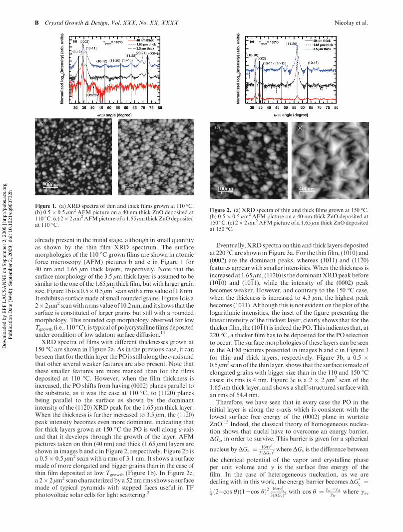
It is well-known that several mechanisms, such as prefer-ential nucleation and growth rate anisotropy of differentcrystal planes, can explain the apparition of texture in poly-crystalline films. It has also been shown that the origin oftextured surface is to be found either in the initial (nucleation)stage or in the growth stage.13 In this work, the evolution ofthe crystallographic orientation with deposited thickness offilms grown at 110 �C is first investigated. In Figure 1a, thelog10 of the X-ray diffraction (XRD) intensity of LPCVDZnO films with various thicknesses is plotted and eachspectrum has been normalized to the maximum of the(0002) peak. Note that we have used the logarithm of theintensities in order to be able to identify even smaller features.It can be seen that for both thin and thick (1.7 and 3.5 μm)layers, the PO growth is along c-axis. In addition to the (0002)peak, several lower intensity features, such as (1011) and(1010), can also be observed in the thicker layer spectra. Thesepeaks are ascribed to non c-axis oriented grains, which are
B Crystal Growth & Design, Vol. XXX, No. XX, XXXX Nicolay et al.
already present in the initial stage, although in small quantityas shown by the thin film XRD spectrum. The surfacemorphologies of the 110 �C grown films are shown in atomicforce microscopy (AFM) pictures b and c in Figure 1 for40 nm and 1.65 μm thick layers, respectively. Note that thesurface morphology of the 3.5 μm thick layer is assumed to besimilar to the one of the 1.65μmthick film, butwith larger grainsize.Figure1b is a0.5� 0.5μm2scanwitha rmsvalueof 1.8nm.It exhibits a surfacemadeof small rounded grains. Figure 1c is a2� 2μm2scanwitha rmsvalueof10.2nm,and it shows that thesurface is constituted of larger grains but still with a roundedmorphology. This rounded cap morphology observed for lowTgrowth (i.e., 110 �C), is typical of polycrystalline films depositedunder condition of low adatom surface diffusion.14
XRD spectra of films with different thicknesses grown at150 �C are shown in Figure 2a. As in the previous case, it canbe seen that for the thin layer thePO is still along the c-axis andthat other several weaker features are also present. Note thatthese smaller features are more marked than for the filmsdeposited at 110 �C. However, when the film thickness isincreased, the PO shifts from having (0002) planes parallel tothe substrate, as it was the case at 110 �C, to (1120) planesbeing parallel to the surface as shown by the dominantintensity of the (1120) XRD peak for the 1.65 μm thick layer.When the thickness is further increased to 3.5 μm, the (1120)peak intensity becomes even more dominant, indicating thatfor thick layers grown at 150 �C the PO is well along a-axisand that it develops through the growth of the layer. AFMpictures taken on thin (40 nm) and thick (1.65 μm) layers areshown in images b and c in Figure 2, respectively. Figure 2b isa 0.5� 0.5 μm2 scan with a rms of 3.1 nm. It shows a surfacemade of more elongated and bigger grains than in the case ofthin film deposited at low Tgrowth (Figure 1b). In Figure 2c,a 2� 2 μm2 scan characterized by a 52 nm rms shows a surfacemade of typical pyramids with stepped faces useful in TFphotovoltaic solar cells for light scattering.2
Eventually,XRDspectra on thin and thick layers depositedat 220 �Care shown in Figure 3a. For the thin film, (1010) and(0002) are the dominant peaks, whereas (1011) and (1120)features appear with smaller intensities.When the thickness isincreasedat 1.65μm, (1120) is the dominantXRDpeakbefore(1010) and (1011), while the intensity of the (0002) peakbecomes weaker. However, and contrary to the 150 �C case,when the thickness is increased to 4.3 μm, the highest peakbecomes (1011).Although this is not evident on the plot of thelogarithmic intensities, the inset of the figure presenting thelinear intensity of the thickest layer, clearly shows that for thethicker film, the (1011) is indeed the PO. This indicates that, at220 �C, a thicker film has to be deposited for the PO selectionto occur. The surfacemorphologies of these layers can be seenin the AFM pictures presented in images b and c in Figure 3for thin and thick layers, respectively. Figure 3b, a 0.5 �0.5μm2 scanof the thin layer, shows that the surface ismadeofelongated grains with bigger size than in the 110 and 150 �Ccases; its rms is 4 nm. Figure 3c is a 2 � 2 μm2 scan of the1.65 μm thick layer, and shows a shelf-structured surface withan rms of 54.4 nm.
Therefore, we have seen that in every case the PO in theinitial layer is along the c-axis which is consistent with thelowest surface free energy of the (0002) plane in wurtziteZnO.15 Indeed, the classical theory of homogeneous nuclea-tion shows that nuclei have to overcome an energy barrier,ΔGc, in order to survive. This barrier is given for a spherical
nucleus byΔGc ¼ 16πγ3
3ðΔGvÞ2 whereΔGv is the difference between
the chemical potential of the vapor and crystalline phaseper unit volume and γ is the surface free energy of thefilm. In the case of heterogeneous nucleation, as we aredealing with in this work, the energy barrier becomes ΔG
�c ¼
14ð2þcos θÞð1-cos θÞ2 16πγ3
fv
3ðΔGvÞ2 with cos θ ¼ γsv -γsfγfv
where γsv
Figure 1. (a) XRD spectra of thin and thick films grown at 110 �C.(b) 0.5 � 0.5 μm2 AFM picture on a 40 nm thick ZnO deposited at110 �C. (c) 2� 2 μm2AFMpicture of a 1.65 μm thickZnOdepositedat 110 �C.
Figure 2. (a) XRD spectra of thin and thick films grown at 150 �C.(b) 0.5 � 0.5 μm2 AFM picture on a 40 nm thick ZnO deposited at150 �C. (c) 2� 2 μm2AFMpicture of a 1.65 μmthick ZnOdepositedat 150 �C.
is the surface energy of the substrate, γsf is the interfacialenergy between the substrate and the film, and γfv is the surfaceenergyof the nucleus. From these equations, it is seen that cosθ= 1 gives the lowest nucleation barrier.16 As a consequence,grainswith the lowest surface free energy,γfv, shouldbe favoredin the nucleation process. However, our growth conditions arefar from thermodynamic equilibrium, notably for the lowTgrowth values, which leads to the apparition of nonminimumsurface free energy (NMSE) grain in the initial layer as seen inthe various XRD spectra of thin and thick films.
Furthermore, the apparition of different POs at 150 and220 �Cwhen the film thickness is increased also points towardnonthermodynamically driven growth and rather indicatesthe predominance of kinetic growth phenomena. Indeed, thefact that a certain growth orientation emerges from the initiallayer, in which it is not the dominant one, is typical of theevolutionary selection theory based on kinetic growthaspects.17,18 Evolutionary selection relies on the growth rateanisotropy of the different crystallographic planes of a mate-rial. It states that the grains having the fastest growingdirection perpendicular to the surface will survive throughthe growth and becomes PO, e.g., in our case, this wouldcorrespond to the (1120) planes at 150 �C or the (1011) planesat 220 �C. On the basis of this theory, it is proposed that thePO and morphology evolutions with the thickness observedon films grown at different Tgrowth values are attributed totemperature-activated growth rate anisotropy of the differentZnO crystallographic plane orientations. As a consequenceand depending on Tgrowth, some initial clusters with givenplanes parallel to the substrate surface would grow faster andat the expense of other grains characterized by a slowervertical growth rate at this temperature. In fact, such avariation in the PO at different temperatures has already been
reported in the literature for MOCVD and sputtered grownZnO.19-21
To have a better understanding of the different phenomenathat could lead to such growth rate anisotropy in our case, wepresent a schematic drawing of the situation for differentTgrowth values in Figure 4. In this figure, two initial clusters areconsidered with different crystallographic orientations paral-lel to the substrate surface, nonminimum surface free energy(NMSE) andminimum surface free energy (MSE) planes. Forthe sake of simplicity, we consider the case of rectangular-shaped clusters inwhich theNMSEandMSEorientations areorthogonal, as is the case in wurtzite ZnO for the [0002] and[1120] directions.
At low Tgrowth (110 �C), the adatoms surface mobility islow. As a consequence, adatoms arriving on the substratesurface are characterized by a low diffusion length and theyhave the tendency to create new clusters with the PO (0002)because of surface free energy minimization, as indicated bythe XRD spectra of thin layers where the (0002) peak isdominant. Regarding adatoms arriving on the grain withNMSE planes parallel to the substrate, they will also havethe tendency to stick at their arrival place because of their lowmobility and the higher dangling bond (DB) density asso-ciated with NMSE planes.22,23 Indeed, the surface free energycan be seen as the excess energy of surface atoms due to thepresence of broken bonds at this surface. Therefore, it isintuitive that facets with higher surface free energy have ahigher DB density.24 This phenomenon contributes to thevertical growth of the grainswithNMSEplanes parallel to thesubstrate. On the contrary, adatoms arriving on MSE facetshave a higher surface diffusivity due to the lowest DB densityof the arrival planes. Therefore, some of these adatoms havethe possibility tomove to the edge of the clusterswhere theDB
Figure 3. (a) XRD spectra of thin and thick films grown at 220 �C. Inset: linear intensity of the XRD on the thickest layer. (b) 0.5 � 0.5 μm2
AFM picture on a 40 nm thick ZnO deposited at 220 �C. (c) 2 � 2 μm2 AFM picture of a 1.65 μm thick ZnO deposited at 220 �C.
Dow
nloa
ded
by E
PF L
AU
SAN
NE
on
Sept
embe
r 2,
200
9 | h
ttp://
pubs
.acs
.org
P
ublic
atio
n D
ate
(Web
): S
epte
mbe
r 2,
200
9 | d
oi: 1
0.10
21/c
g900
732h
D Crystal Growth & Design, Vol. XXX, No. XX, XXXX Nicolay et al.
density is higher (as the lateral face is a NMSE plane), whichcontributes to their lateral expansion. However, this lateralexpansion should be limited because of the low Tgrowth. Inaddition, as it has been observed that at Tgrowth = 110 �C thePO is (0002) for thin and thick layers, it is proposed that thelarger amount of clusters forming with the MSE, (0002),planes and their higher lateral growth rate dominates thefew clusterswithNMSEplanesparallel to the substrate,whichgrow vertically at an insufficient rate to shadow the growth ofthe MSE clusters. In fact, it is supposed that the verticalgrowth rate of both MSE and NMSE clusters are similar atlow Tgrowth.
At intermediate Tgrowth (150-220 �C), the adatoms have ahigher surface mobility due to the higher temperature. Hence,instead of creating new MSE clusters, adatoms arriving closeto the edge of the NMSE grains have the possibility to diffusefrom their lateral MSE facets, characterized by a low DBdensity, and to jump on the NMSE planes of these grainswhere the DB density is higher. As a consequence of thisinterfacet diffusion, the NMSE clusters have a higher adatomconcentration on their NMSE facets, resulting in a highervertical growth rate compared to the lowTgrowth case but alsocompared to their own lateral growth rate.22,23 It is alsointeresting to note that by piling up atoms vertically, theexposed surface of NMSE planes is not increased while thesize of their lateral MSE facets is increased, which alsocontributes to a minimization of the grain surface free en-ergy.25 Regarding initial cluster with MSE planes parallel to
the substrate, the higher adatom surface diffusivity due toboth the higher Tgrowth and to the lower DB density of theseplanes, leads to a decreased adatom density on their horizon-tal surfaces, which decreases their vertical growth rate. In thiscase, the increased vertical growth rate of the NMSE clustersdominates the vertical and lateral expansion of the grainswithMSE planes parallel to the substrate. Therefore, as predictedby the evolutionary selection, clusters that have the NMSEplanes parallel to the substrate in the initial stage will survivethrough the growth. This explains why the (1120) peak of theXRD spectrum of the films grown at 150 �C (the peak thatcorresponds to NMSE planes parallel to the surface) has firsta smaller intensity relatively to the other peaks of the thinlayer, and then becomes the dominant crystallographic or-ientation in the thick layers. Such a grain growth competitionalso leads to the peculiar TEM structures observed in ref 10,where some grains emerge at the surface while being enclosedby others.26 The predominance of NMSE clusters that have ahigher vertical growth rate than their own lateral growth ratealso explains the stepped pyramidal shape of the surfacefeatures characteristic of the thick layers grown in this tem-perature range. Regarding the layers deposited at 220 �C, theemergence of the (1011) peak in the XRD spectrum of a thicklayer is ascribed to the increase in the adatom surfacemobilitybecause of the higher Tgrowth, leading to the selection ofNMSE with another PO as the thickness is increased. It alsoseems that the growth competition between differently or-iented NMSE clusters leads to the fact that one needs todeposit a thicker layer to see a definitive PO emerging at thistemperature. The increased adatommobility can also explainwhy in thin layer deposited at 150 and 220 �C, XRD spectrashow several peaks with intensities comparable to the one ofthe (0002) feature. Indeed, as explained before, because oftheir higher diffusive ability, adatoms can jumpon the surfaceof NMSE clusters instead of forming new grains directly onthe substrate with (0002) planes parallel to the surface; this inturn reduces the relative intensity of the c-axis peak andincreases the one of the NMSE clusters.
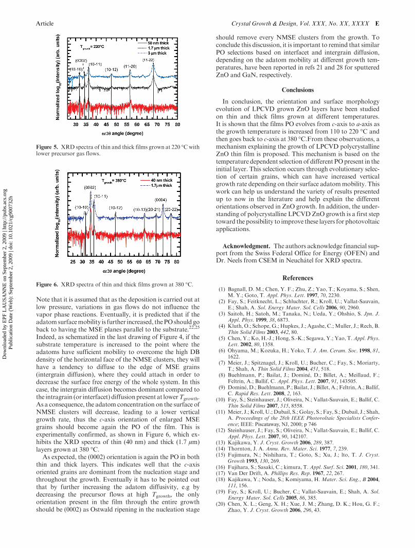
To summarize, it is proposed that depending on the surfacemobility of the arriving adatoms (which is increased as thegrowth temperature is increased), interfacets diffusion canoccur, which leads to the fact that grains with NMSE planesparallel to the surface have a dominant vertical growth rateallowing them to emerge through the growth. To further testthis hypothesis, we have deposited thin (50 nm) and thicklayers (1.7 and 3μm) at 220 �Cwith reduced flowsofDEZandH2O,which were respectively set to 10 and 20 sccm in order tokeep a H2O/DEZ ratio similar to the one used for thedeposition of the previous films. By decreasing the reactantflows, it is assumed that the adatom mobility is increased asthe surface atoms have more possibility to move before beingfrozen by new incoming atoms. In accordancewith anadatommobility-driven PO selection process, the increased adatomsurface mobility led to the apparition of a new NMSE PO,(1122), in the deposited film, as shown in the XRD spectra ofFigure 5.
Again, in this figure it can be seen that several orientationsare dominant in the initial stage, whereas the (1122) orienta-tion becomes PO only as the thickness is increased. In addi-tion, the apparition of this new PO by simply changing theflow rates also discards the possibility that we are dealingwitha chemically driven PO growth in which ionic radicals thatwould be present at differentTgrowth in the vapor phase wouldinhibit certain growth directions, as was proposed in ref 27.
Figure 4. Schematic drawing of PO selection mechanisms at differ-ent Tgrowth values.
Note that it is assumed that as the deposition is carried out atlow pressure, variations in gas flows do not influence thevapor phase reactions. Eventually, it is predicted that if theadatomsurfacemobility is further increased, thePOshould goback to having the MSE planes parallel to the substrate.22,25
Indeed, as schematized in the last drawing of Figure 4, if thesubstrate temperature is increased to the point where theadatoms have sufficient mobility to overcome the high DBdensity of the horizontal face of the NMSE clusters, they willhave a tendency to diffuse to the edge of MSE grains(intergrain diffusion), where they could attach in order todecrease the surface free energy of the whole system. In thiscase, the intergrain diffusion becomes dominant compared tothe intragrain (or interfacet) diffusionpresent at lowerTgrowth.As a consequence, the adatom concentration on the surface ofNMSE clusters will decrease, leading to a lower verticalgrowth rate, thus the c-axis orientation of enlarged MSEgrains should become again the PO of the film. This isexperimentally confirmed, as shown in Figure 6, which ex-hibits the XRD spectra of thin (40 nm) and thick (1.7 μm)layers grown at 380 �C.
As expected, the (0002) orientation is again the PO in boththin and thick layers. This indicates well that the c-axisoriented grains are dominant from the nucleation stage andthroughout the growth. Eventually it has to be pointed outthat by further increasing the adatom diffusivity, e.g bydecreasing the precursor flows at high Tgrowth, the onlyorientation present in the film through the entire growthshould be (0002) as Ostwald ripening in the nucleation stage
should remove every NMSE clusters from the growth. Toconclude this discussion, it is important to remind that similarPO selections based on interfacet and intergrain diffusion,depending on the adatom mobility at different growth tem-peratures, have been reported in refs 21 and 28 for sputteredZnO and GaN, respectively.
Conclusions
In conclusion, the orientation and surface morphologyevolution of LPCVD grown ZnO layers have been studiedon thin and thick films grown at different temperatures.It is shown that the films PO evolves from c-axis to a-axis asthe growth temperature is increased from 110 to 220 �C andthen goes back to c-axis at 380 �C.From these observations, amechanism explaining the growth of LPCVD polycrystallineZnO thin film is proposed. This mechanism is based on thetemperature dependent selection of different POpresent in theinitial layer. This selection occurs through evolutionary selec-tion of certain grains, which can have increased verticalgrowth rate depending on their surface adatommobility. Thiswork can help us understand the variety of results presentedup to now in the literature and help explain the differentorientations observed in ZnO growth. In addition, the under-standing of polycrystalline LPCVDZnO growth is a first steptoward the possibility to improve these layers for photovoltaicapplications.
Acknowledgment. The authors acknowledge financial sup-port from the Swiss Federal Office for Energy (OFEN) andDr. Neels from CSEM in Neuchatel for XRD spectra.
References
(1) Bagnall, D. M.; Chen, Y. F.; Zhu, Z.; Yao, T.; Koyama, S.; Shen,M. Y.; Goto, T. Appl. Phys. Lett. 1997, 70, 2230.
(2) Fay, S.; Feitknecht, L.; Schluchter, R.; Kroll, U.; Vallat-Sauvain,E.; Shah, A. Sol. Energy Mater. Sol. Cells 2006, 90, 2960.
(3) Saitoh, H.; Satoh, M.; Tanaka, N.; Ueda, Y.; Ohshio, S. Jpn. J.Appl. Phys. 1999, 38, 6873.