w WAN_0118 Guidelines on How to Use QFN Packages and Create Associated PCB Footprints WOLFSON MICROELECTRONICS plc To receive regular email updates, sign up at http://www.wolfsonmicro.com/enews/ January 2006, Rev 2.1 Copyright 2006 Wolfson Microelectronics plc INTRODUCTION The Quad Fine Pitch No Leads (QFN) package is a leadless plastic package, which obtains electrical contact via lands on the bottom surface of the device. Its compact nature and low profile makes the QFN package ideal for designs where space considerations are at a premium. This small size is one of the main reasons why the QFN package is chosen for Wolfson Microelectronics devices for portable applications. In addition to the bottom surface mounted pins, the other distinguishing feature of this package type is the exposed die paddle on the bottom side of the device. This paddle can be used to add extra strength in PCB mounting and to conduct heat more efficiently away from the die. The paddle may in future be bonded as a further analogue ground and so it is recommended that it be connected to the analogue ground of the PCB it is mounted to. This Application note sets out to explain some of the issues related to the design of a PCB footprint for the QFN package and then goes on to describe practical considerations when soldering the device to a PCB. PACKAGE DIMENSIONS The first thing to consider when creating a QFN footprint is the package drawing for the device. Wolfson uses a number of different QFN packages based on JEDEC specifications as follows: SIZE PIN WOLFSON TYPE 4MM×4MM 24 C 5MM×5MM 28 A 5MM×5MM 32 A AND C 6MM×6MM 40 C 7MM×7MM 48 C 9MM×9MM 64 C Figure 1 QFN Package Range
Transcript
w WAN_0118
Guidelines on How to Use QFN Packages and Create Associated PCB Footprints
WOLFSON MICROELECTRONICS plc
To receive regular email updates, sign up at http://www.wolfsonmicro.com/enews/
January 2006, Rev 2.1
Copyright 2006 Wolfson Microelectronics plc
INTRODUCTION
The Quad Fine Pitch No Leads (QFN) package is a leadless plastic package, which obtains electrical contact via lands on the bottom surface of the device. Its compact nature and low profile makes the QFN package ideal for designs where space considerations are at a premium. This small size is one of the main reasons why the QFN package is chosen for Wolfson Microelectronics devices for portable applications.
In addition to the bottom surface mounted pins, the other distinguishing feature of this package type is the exposed die paddle on the bottom side of the device. This paddle can be used to add extra strength in PCB mounting and to conduct heat more efficiently away from the die. The paddle may in future be bonded as a further analogue ground and so it is recommended that it be connected to the analogue ground of the PCB it is mounted to.
This Application note sets out to explain some of the issues related to the design of a PCB footprint for the QFN package and then goes on to describe practical considerations when soldering the device to a PCB.
PACKAGE DIMENSIONS
The first thing to consider when creating a QFN footprint is the package drawing for the device. Wolfson uses a number of different QFN packages based on JEDEC specifications as follows:
The Wolfson QFN package currently has two types of lead termination features, these are as follows.
WOLFSON TYPE A
The Wolfson Type A package is based on the JEDEC MO-220 specification with a slight modification on the pad design. In the Type A package there is mould compound round the bottom corner of the package (see arrow). After reflow a solder fillet between the PCB and the side of the package is not required; the side of the package is not required to be solderable. This is as defined in international standard IPC-A-610D. Refer to extract in the Appendix.
Figure 2 Type A QFN Package
WOLFSON TYPE C
The Type C package is based on the JEDEC MO-220 specification with pads that are extended up the side of the package. After reflow a solder fillet between the PCB and the side of the package is not required; the side of the package is not required to be solderable. This is as defined in international standard IPC-A-610D. Refer to extract in the Appendix.
Figure 3 Type C QFN Package
The package type is dependant on the types of the part supplied and product family and can be found in the product data sheet. The dimension of the packages are, at time of document release, as follows. Please refer to the individual datasheets for the most current issue of the package dimensions.
WAN_0118
w January 2006, Rev 2.1
3
DM035.CFL: 24 PIN QFN PLASTIC PACKAGE 4 X 4 X 0.9 mm BODY, 0.50 mm LEAD PITCH
INDEX AREA(D/2 X E/2)
TOP VIEW
D
E
4
NOTES:1. DIMENSION b APPLIES TO METALLIZED TERMINAL AND IS MEASURED BETWEEN 0.15 mm AND 0.30 mm FROM TERMINAL TIP.2. FALLS WITHIN JEDEC, MO-220, VARIATION VGGD-2.3. ALL DIMENSIONS ARE IN MILLIMETRES.4. THE TERMINAL #1 IDENTIFIER AND TERMINAL NUMBERING CONVENTION SHALL CONFORM TO JEDEC 95-1 SPP-002.5. COPLANARITY APPLIES TO THE EXPOSED HEAT SINK SLUG AS WELL AS THE TERMINALS.6. REFER TO APPLICATIONS NOTE WAN_0118 FOR FURTHER INFORMATION REGARDING PCB FOOTPRINTS AND QFN PACKAGE SOLDERING.7. DEPENDING ON THE METHOD OF LEAD TERMINATION AT THE EDGE OF THE PACKAGE, PULL BACK (L1) MAY BE PRESENT.8. THIS DRAWING IS SUBJECT TO CHANGE WITHOUT NOTICE.
A3G
T
H
W
bExposed lead Half etch tie bar
Dimensions (mm)SymbolsMIN NOM MAX NOTE
AA1A3
0.80 0.90 1.000.050.020
0.20 REF
bDD2EE2e
L
0.300.184.00
2.252.152.00
0.50 BSC
0.30 0.40 0.50
2
24.00
2.252.152.00
0.10aaabbbccc
REF:
0.15
0.10
JEDEC, MO-220, VARIATION VGGD-2.
Tolerances of Form and Position
0.25
H 0.10.213G
T 0.1
W 0.2
DETAIL 1
DETAIL 2
A
6
1
13
18
2419
12
e
D2
b7 1BCbbbM A
BOTTOM VIEW
Caaa2 X
Caaa2 X
1
C
A3
SEATING PLANE DETAIL 2
A1
C0.08
Cccc
A5
SIDE VIEW
L
L1
L1 0.150.03 7
EXPOSEDGROUNDPADDLE
6
DETAIL 1
0.32mm
45degrees
EXPOSEDGROUNDPADDLE
e
Datum
DETAIL 2
Terminaltipe/2
1
R
E2
SEE DETAIL 2
Figure 4 24 pin 4x4 QFN Package Wolfson Type C
WAN_0118
w January 2006, Rev 2.1
4
NOTES:1. DIMENSION b APPLIED TO METALLIZED TERMINAL AND IS MEASURED BETWEEN 0.25 mm AND 0.30 mm FROM TERMINAL TIP. DIMENSION L1 REPRESENTS TERMINAL PULL BACK FROM PACKAGE SIDE WALL. MAXIMUM OF 0.1mm IS ACCEPTABLE. WHERE TERMINAL PULL BACK EXISTS, ONLY UPPER HALF OF LEAD IS VISIBLE ON PACKAGE SIDE WALL DUE TO HALF ETCHING OF LEADFRAME.2. FALLS WITHIN JEDEC, MO-220 WITH THE EXCEPTION OF D2, E2: D2,E2: LARGER PAD SIZE CHOSEN WHICH IS JUST OUTSIDE JEDEC SPECIFICATION3. ALL DIMENSIONS ARE IN MILLIMETRES4. THIS DRAWING IS SUBJECT TO CHANGE WITHOUT NOTICE.5. SHAPE AND SIZE OF CORNER TIE BAR MAY VARY WITH PACKAGE TERMINAL COUNT. CORNER TIE BAR IS CONNECTED TO EXPOSED PAD INTERNALLY6. REFER TO APPLICATION NOTE WAN_0118 FOR FURTHER INFORMATION REGARDING PCB FOOTPRINTS AND QFN PACKAGE SOLDERING.
DM023.GFL: 28 PIN QFN PLASTIC PACKAGE 5 X 5 X 0.9 mm BODY, 0.50 mm LEAD PITCH
Caaa
INDEX AREA(D/2 X E/2)
Caaa2 X
2 X
TOP VIEW
D
E
C0.08
Cccc
A
A1C
(A3)
SEATING PLANE
1
14 13 b
15
L
D2/2
D2
E2
E2/2
SEE DETAIL B
BCccc M A
B
B
A A
27 28
1
2
7
8
21
22
e
5
CORNERTIE BAR
DETAIL A
BCbbb M A28x b
L28
x K
L1
R
1
1
0.566 mm
5
CORNERTIE BAR
0.15
DETAIL B
TE
RM
INA
L T
IP
R
DA
TU
M
ee/
2
L1
1
SEE DETAIL A
SymbolsDimensions (mm)
MIN NOM MAX NOTEA
A1A3bD
D2E
E2eL
L1R
0.85 0.90 1.000.050.020
0.2 REF0.300.230.18
5.00 BSC3.43.33.2
5.00 BSC
0.5 BSC3.3 3.43.2
0.35 0.4 0.450.1
b(min)/2
1
2
2
1
K 0.20
aaabbbccc
REF:
0.150.100.10
JEDEC, MO-220, VARIATION VHHD-1
Tolerances of Form and Position
EXPOSEDGROUNDPADDLE
EXPOSEDGROUNDPADDLE
6
BOTTOM VIEW
SIDE VIEW
0.38mm
0.210mm
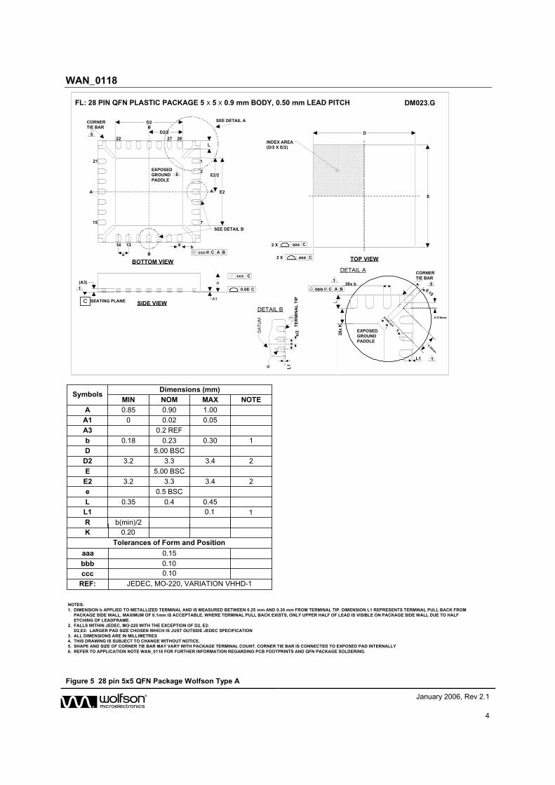
Figure 5 28 pin 5x5 QFN Package Wolfson Type A
WAN_0118
w January 2006, Rev 2.1
5
DM030.EFL: 32 PIN QFN PLASTIC PACKAGE 5 X 5 X 0.9 mm BODY, 0.50 mm LEAD PITCH
NOTES:1. DIMENSION b APPLIED TO METALLIZED TERMINAL AND IS MEASURED BETWEEN 0.25 mm AND 0.30 mm FROM TERMINAL TIP. DIMENSION L1 REPRESENTS TERMINAL PULL BACK FROM PACKAGE SIDE WALL. MAXIMUM OF 0.1mm IS ACCEPTABLE. WHERE TERMINAL PULL BACK EXISTS, ONLY UPPER HALF OF LEAD IS VISIBLE ON PACKAGE SIDE WALL DUE TO HALF ETCHING OF LEADFRAME.2. FALLS WITHIN JEDEC, MO-220 WITH THE EXCEPTION OF D2, E2: D2,E2: LARGER PAD SIZE CHOSEN WHICH IS JUST OUTSIDE JEDEC SPECIFICATION3. ALL DIMENSIONS ARE IN MILLIMETRES4. THIS DRAWING IS SUBJECT TO CHANGE WITHOUT NOTICE.5. SHAPE AND SIZE OF CORNER TIE BAR MAY VARY WITH PACKAGE TERMINAL COUNT. CORNER TIE BAR IS CONNECTED TO EXPOSED PAD INTERNALLY.6. REFER TO APPLICATION NOTE WAN_0118 FOR FURTHER INFORMATION REGARDING PCB FOOTPRINTS AND QFN PACKAGE SOLDERING.
SEE DETAIL BE2
E2/2
bB
16 15
A
8
9
e
5
CORNERTIE BAR B
D2
L
D2/2
SEE DETAIL A
INDEX AREA(D/2 X E/2)
TOP VIEW
D
Caaa2 X
Caaa2 X
E
DETAIL B
TE
RM
INA
L T
IP
R
DA
TU
M
ee/
2
L1
1
DETAIL A
BCbbb M A32x b
L32
x K
L1
R
1
1
0.566 mm
0.43 mm
5
CORNERTIE BAR
Symbols Dimensions (mm)MIN NOM MAX NOTE
AA1A3bDD2EE2eLL1R
0.85 0.90 1.000.050.020
0.2 REF0.300.230.18
5.003.43.33.2
0.5 BSC0.35 0.4 0.45
0.1b(min)/2
1
2
2
1
K 0.20
aaabbbccc
REF:
0.150.100.10
JEDEC, MO-220, VARIATION VHHD-2
Tolerances of Form and Position
4.90 5.10
5.004.90 5.10
3.43.33.2
1
17
24
25 32
EXPOSEDGROUNDPADDLE
6
EXPOSEDGROUNDPADDLE
BOTTOM VIEW
C0.08
Cccc
A
A1C
(A3)
SEATING PLANE
1
SIDE VIEW
Figure 6 32 pin 5x5 QFN Package Wolfson Type A
WAN_0118
w January 2006, Rev 2.1
6
DM033.DFL: 32 PIN QFN PLASTIC PACKAGE 5 X 5 X 0.9 mm BODY, 0.50 mm LEAD PITCH
E2
bB
16 15
A
8
9
e
C0.08
Cccc
A
A1C
A3
SEATING PLANE
1
L
INDEX AREA(D/2 X E/2)
TOP VIEW
D
Caaa2 X
Caaa2 X
E
1
17
24
25 32
D2
BCbbbM A
5
4
NOTES:1. DIMENSION b APPLIES TO METALLIZED TERMINAL AND IS MEASURED BETWEEN 0.15 mm AND 0.30 mm FROM TERMINAL TIP.2. FALLS WITHIN JEDEC, MO-220, VARIATION VHHD-5.3. ALL DIMENSIONS ARE IN MILLIMETRES.4. THE TERMINAL #1 IDENTIFIER AND TERMINAL NUMBERING CONVENTION SHALL CONFORM TO JEDEC 95-1 SPP-002.5. COPLANARITY APPLIES TO THE EXPOSED HEAT SINK SLUG AS WELL AS THE TERMINALS.6. REFER TO APPLICATION NOTE WAN_0118 FOR FURTHER INFORMATION REGARDING PCB FOOTPRINTS AND QFN PACKAGE SOLDERING.7. THIS DRAWING IS SUBJECT TO CHANGE WITHOUT NOTICE.
DETAIL 1
R = 0.3MM
A3G
T
H
W
bExposed lead Half etch tie bar
Dimensions (mm)SymbolsMIN NOM MAX NOTE
AA1A3
0.80 0.90 1.000.050.020
0.20 REF
bDD2EE2e
L
0.300.185.00
3.553.453.30
0.50 BSC
0.30 0.40 0.50
1
2
25.00
3.553.453.30
0.10aaabbbccc
REF:
0.15
0.10
JEDEC, MO-220, VARIATION VHHD-5.
Tolerances of Form and Position
0.25
H 0.10.213G
T 0.1
W 0.2
DETAIL 1
DETAIL 2
DETAIL 2
EXPOSEDGROUNDPADDLE
6
EXPOSEDGROUNDPADDLE
BOTTOM VIEW
SIDE VIEW
Figure 7 32 pin 5x5 QFN Package Wolfson Type C
WAN_0118
w January 2006, Rev 2.1
7
DM037.BFL: 40 PIN QFN PLASTIC PACKAGE 6 X 6 X 0.9 mm BODY, 0.50 mm LEAD PITCH
NOTES:1. DIMENSION b APPLIES TO METALLIZED TERMINAL AND IS MEASURED BETWEEN 0.15 mm AND 0.30 mm FROM TERMINAL TIP.2. FALLS WITHIN JEDEC, MO-220, VARIATION VJJD-2.3. ALL DIMENSIONS ARE IN MILLIMETRES.4. THE TERMINAL #1 IDENTIFIER AND TERMINAL NUMBERING CONVENTION SHALL CONFORM TO JEDEC 95-1 SPP-002.5. COPLANARITY APPLIES TO THE EXPOSED HEAT SINK SLUG AS WELL AS THE TERMINALS.6. REFER TO APPLICATION NOTE WAN_0118 FOR FURTHER INFORMATION REGARDING PCB FOOTPRINTS AND QFN PACKAGE SOLDERING.7. DEPENDING ON THE METHOD OF LEAD TERMINATION AT THE EDGE OF THE PACKAGE, PULL BACK (L1) MAY BE PRESENT.8. THIS DRAWING IS SUBJECT TO CHANGE WITHOUT NOTICE.
AA1A3
0.80 0.90 1.000.050.020
0.20 REF
bDD2EE2e
L
0.300.186.00 BSC
4.254.154.00
0.50 BSC
0.30 0.40 0.50
2
26.00 BSC
4.254.154.00
0.10aaabbbccc
REF:
0.15
0.10
JEDEC, MO-220, VARIATION VJJD-2.
Tolerances of Form and Position
0.25
H 0.10.213G
T 0.1
W 0.2
DETAIL 2
1
DETAIL 1
INDEX AREA(D/2 X E/2)
TOP VIEW
D
E
4
DETAIL 1
BOTTOM VIEW
Caaa2 X
Caaa2 X
E2
10
1
e
b 1BCbbbM A
D2
A
21
30
4031
1120
C
A3
SEATING PLANE
SIDE VIEW
DETAIL 2
A1
C0.08
Cccc
A5
A3G
T
H
bExposed lead Half etch tie bar
W
7AA
DD CCBB
LL1
Dimensions (mm)SymbolsMIN NOM MAX NOTE
Dimensions (mm)Symbols
MIN NOM MAX NOTEAA 0.235
L1DDCCBB
0.150.030.1810.1810.235
7
7
77
EXPOSEDGROUNDPADDLE
6
Figure 8 40 pin 6x6 QFN Package Wolfson Type C
WAN_0118
w January 2006, Rev 2.1
8
e
DM029.EFL: 48 PIN QFN PLASTIC PACKAGE 7 X 7 X 0.9 mm BODY, 0.50 mm LEAD PITCH
INDEX AREA(D/2 X E/2)
TOP VIEW
Caaa2 X
SEE DETAIL 2
E2
E2/2
b
D2
24
L
D2/2
Caaa2 X
25
36
37 48
1
12
13
D
E
e
Datum
SEE DETAIL 1
C0.08
Cccc
A
A1C
(A3)
SEATING PLANE
DETAIL 3
DETAIL 3
DETAIL 2
Terminaltip
R
e/2
1
DETAIL 1
(A3)G
T
H
W
bExposed lead Half etch tie bar
Symbols Dimensions (mm)MIN NOM MAX NOTE
A
bDD2EE2e
L
0.80 0.90 1.00
0.300.250.187.00 BSC
5.255.155.007.00 BSC
0.5 BSC5.15 5.255.00
0.30 0.4 0.50
1
A1A3
0 0.02 0.050.20 REF
GH
0.2130.1
NOTES:1. DIMENSION b APPLIED TO METALLIZED TERMINAL AND IS MEASURED BETWEEN 0.15 mm AND 0.30 mm FROM TERMINAL TIP.2. ALL DIMENSIONS ARE IN MILLIMETRES3. THE TERMINAL #1 IDENTIFIER AND TERMINAL NUMBERING CONVENTION SHALL CONFORM TO JESD 95-1 SPP-002.4. COPLANARITY APPLIES TO THE EXPOSED HEAT SINK SLUG AS WELL AS THE TERMINALS.5. THIS DRAWING IS SUBJECT TO CHANGE WITHOUT NOTICE.6. REFER TO APPLICATION NOTE WAN_0118 FOR FURTHER INFORMATION REGARDING PCB FOOTPRINTS AND QFN PACKAGE SOLDERING.
JEDEC, MO-220, VARIATION VKKD-2
Tolerances of Form and Position
TW
aaabbbccc
0.10.2
0.150.100.10
REF
EXPOSEDGROUNDPADDLE
6
R = 0.3MM
EXPOSEDGROUNDPADDLE
BOTTOM VIEW
SIDE VIEW
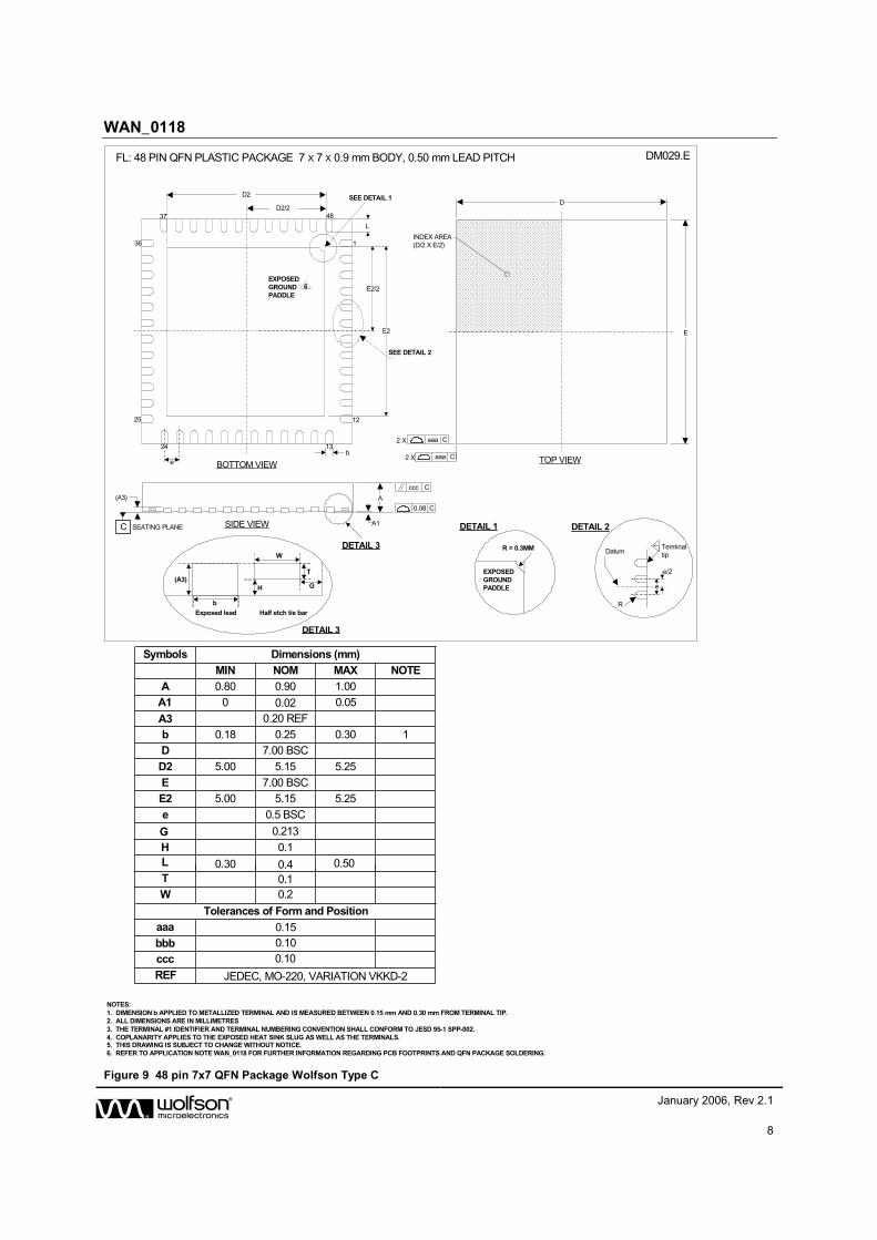
Figure 9 48 pin 7x7 QFN Package Wolfson Type C
WAN_0118
w January 2006, Rev 2.1
9
e
DM039.BFL: 64 PIN QFN PLASTIC PACKAGE 9 X 9 X 0.9 mm BODY, 0.50 mm LEAD PITCH
INDEX AREA(D/2 X E/2)
TOP VIEW
Caaa2 X
SEE DETAIL 2
E2
E2/2
b
D2
32
L
D2/2
Caaa2 X
33
48
49 64
1
16
17
D
E
Datum
SEE DETAIL 1
C0.08
Cccc
A
A1C
(A3)
SEATING PLANE
DETAIL 3
DETAIL 3
DETAIL 2
Terminaltip
R
e/2
1
DETAIL 1
0.35mm
45degrees
(A3)G
T
H
W
bExposed lead Half etch tie bar
Symbols Dimensions (mm)MIN NOM MAX NOTE
A
bDD2EE2e
L
0.80 0.90 1.00
0.300.250.189.00 BSC
7.257.157.009.00 BSC
0.5 BSC7.15 7.257.00
0.30 0.40 0.50
1
A1A3
0 0.02 0.050.20 REF
GH
0.1650.1
NOTES:1. DIMENSION b APPLIED TO METALLIZED TERMINAL AND IS MEASURED BETWEEN 0.15 mm AND 0.30 mm FROM TERMINAL TIP.2. ALL DIMENSIONS ARE IN MILLIMETRES3. THE TERMINAL #1 IDENTIFIER AND TERMINAL NUMBERING CONVENTION SHALL CONFORM TO JESD 95-1 SPP-002.4. COPLANARITY APPLIES TO THE EXPOSED HEAT SINK SLUG AS WELL AS THE TERMINALS.5. THIS DRAWING IS SUBJECT TO CHANGE WITHOUT NOTICE.6. REFER TO APPLICATION NOTE WAN_0118 FOR FURTHER INFORMATION REGARDING PCB FOOTPRINTS AND QFN PACKAGE SOLDERING.
Tolerances of Form and Position
TW
aaabbbccc
0.10.2
0.150.100.10
REF
e
JEDEC, MO-220, VARIATION VMMD-2
BOTTOM VIEW
SIDE VIEW
EXPOSEDGROUNDPADDLE
6
Figure 10 64 pin 9x9 QFN Package Wolfson Type C
WAN_0118
w January 2006, Rev 2.1
10
PCB DESIGN CONSIDERATIONS
The PCB design rules when using the QFN packages are fundamentally no different to those for other more well known packages. The most important considerations are those effects that occur during the PCB assembly process, which do affect the PCB land layout.
The most obvious difference is the presence of a large thermal die paddle on the bottom side of the device. Concern is also often shown to the pull-off strength of the QFN device when simply using the pads to fix the package. For added strength and improved thermal dissipation characteristics, the die paddle should ideally be soldered to the PCB in addition to the pins.
ROUTING OF TRACES
Traces should be routed straight out from the peripheral pads to a minimum of 500um beyond the device extremities. Traces should not be routed inwards to a via at the expense of all or part of the thermal die paddle as there would be a strong possibility of the via shorting to the die paddle. For QFN Type A packages (see Figures 5 & 6 above) traces from the corner pads should not be routed perpendicularly as there would be a strong possibility of the trace shorting to the corner tie bars. This corner area should also be free of other signal traces or copper plane areas that are connected to different ground planes than that of the die paddle. Figure 17 below, shows a good example layout where all of the above and below recommendations have been considered and adhered to.
THERMAL DISSIPATION
To allow the heat generated through this large pad to dissipate, the area under the device may require the inclusion of a thermal landing on the component side of the PCB equal in size to the maximum size of the device thermal die paddle (it is also recommended to place a thermal landing on the opposite side of the PCB) connected to analogue ground using a number of thermal vias, approximately 0.33mm (0.013 inches) diameter. These thermal vias should be completely connected (flooded over) to the thermal landing(s) (as well as internal ground planes if using a multilayer PCB) and should not be confused with “thermal relief” or “web-constructed” vias which are designed with “spokes” to decrease thermal transfer through the PCB. The number of vias will depend upon device package size, but as a guide the pitch between the vias should be between 0.74mm and 1.27mm. In Figures 11 – 15 below, 3x3 vias are used for the packages. In Figure 16, the 9X9 package’s size allows an additional 8 vias. Figures 11 - 16 are not to scale for the purpose of clarity.
WAN_0118
w January 2006, Rev 2.1
11
QFN FOOTPRINTS DIMENSIONS
Figure 11 24 Pin 4x4 QFN Footprint
Figure 12 28 Pin 5x5 QFN Footprint
Figure 13 32 Pin 5x5 QFN Footprint
WAN_0118
w January 2006, Rev 2.1
12
Figure 14 40 Pin 6x6 QFN Footprint
Figure 15 48 Pin 7x7 QFN Footprint
Figure 16 64 Pin 9x9 QFN Footprint
WAN_0118
w January 2006, Rev 2.1
13
SOLDER MASK AND STENCIL DESIGN CONSIDERATIONS
The greater complexity of the QFN footprint due to the inclusion of the die paddle also means that the solder mask used during assembly will be of equal complexity. To prevent the solder of the die paddle transgressing onto the land pads during reflow, the solder mask should overlap the thermal pad outer edges by at least 100um. This overlap will prevent transgression to the land pads even in the worst case scenario.
As per Figure 17, the vias should be left bare or untented. This minimizes the presence of voids and prevents outgassing during reflow. Additionally, if the application permits the use of plated through hole vias, then the bottom side soldermask should have a clearance around the vias equal in size to the one on the top side.
Figure 17 32 Pin 5x5 QFN Design Guide
STENCIL DESIGN FOR PERIMETER PADS
The stencil should be 1:1 or 90% of the PCB pad size and should be laser cut for accuracy and electro-polished which helps in smoothing the stencil sidewalls. The recommended stencil thickness used is 0.075mm to 0.127mm (0.003in to 0.005in) and the sidewalls of the stencil openings should be tapered approximately 5 degrees to facilitate better paste release.
DISSECTION OF THE DIE PADDLE SOLDER PASTE STENCIL
If the solder paste coverage of the thermal landing is too big, out-gassing occurs during the reflow process which may cause defects (splatter, solder balling). As per Figure 17, dividing the thermal landing into smaller screen openings reduces the risk of solder voiding and allows the solder joints for the smaller terminal pads to be at the same height as the larger ones. Figure 17 also shows how the solder paste stencil pattern can minimize the risk of the solder paste wicking down untented vias.
WAN_0118
w January 2006, Rev 2.1
14
SOLDER PASTE RECOMMENDATIONS AND REFLOW PROFILE
Due to the size, pitch and depth of the stencil apertures for the QFN package it is recommended that type 3 no-clean solder pastes be used for printing. For reflow it is recommended an IR or Forced Convection system be used or a combination system of IR and Forced Convection. For further information on soldering, please refer to Wan_0158.
INSPECTION OF SOLDER JOINTS AFTER REFLOW
Due to the pad layout of the QFN the solder joints are formed underneath the package and are not visible. It is recommended that to ensure the joints are soldered sufficiently x-ray inspection be utilized whenever possible. Visual inspection may be used for a cursory inspection to ensure that there is no obvious solder bridging.
Shown below in Figure 18 is a typical x-ray inspection of the Wolfson 32pin QFN.
Figure 18 X-Ray Inspection of 5mm×5mm 32 pin QFN
As can be seen the solder has reflowed to form acceptable joints and there is minimal voiding in the thermal die paddle and pad solder joints, also there is no bridging visible between the joints. X-Ray inspection can also be useful in highlighting possible process problems such as solder balling and voiding which are often an indication of poorly optimized reflow profiles.
For a cursory visual inspection it should be noted that Wolfson currently provides its packages with two different QFN package types as mentioned. However it should be noted that solder fillets up the side of the QFN package are not required for acceptability of soldering; as specified in international standard IPC-A-610D; whether fillets are formed or not does not affect the mechanical strength and reliability of the solder joints. There is no difference in the mechanical strength and reliability between the two packages; the differences are only cosmetic.
WAN_0118
w January 2006, Rev 2.1
15
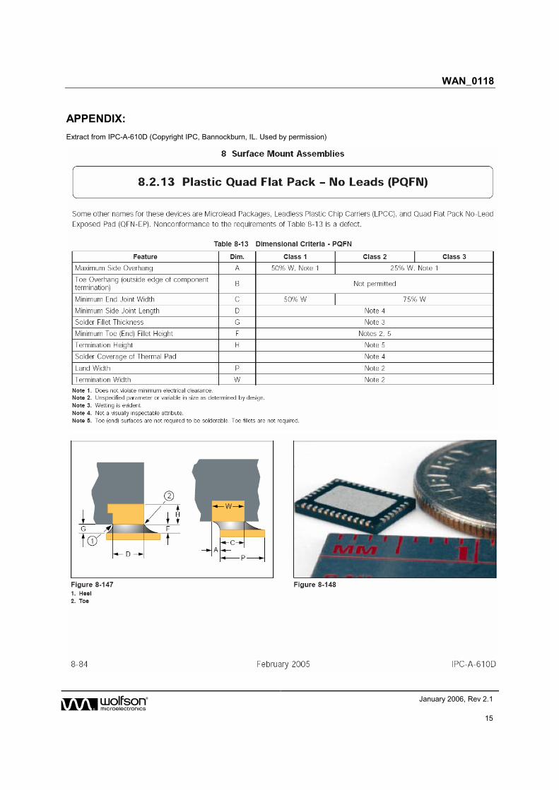
APPENDIX:
Extract from IPC-A-610D (Copyright IPC, Bannockburn, IL. Used by permission)
WAN_0118
w January 2006, Rev 2.1
16
WAN_0118
w January 2006, Rev 2.1
17
APPLICATION SUPPORT
If you require further information or require technical support, please contact Wolfson Microelectronics Applications group through the following channels:
Email: [email protected] Telephone: (+44) 131 272 7070 Fax: (+44) 131 272 7001 Mail: Applications at the address on the last page.
or contact your local Wolfson representative.
Additional information may be made available from time to time on our web site at: http://www.wolfsonmicro.com
WAN_0118
w January 2006, Rev 2.1
18
IMPORTANT NOTICE Wolfson Microelectronics plc (WM) reserve the right to make changes to their products or to discontinue any product or service without notice, and advise customers to obtain the latest version of relevant information to verify, before placing orders, that information being relied on is current. All products are sold subject to the WM terms and conditions of sale supplied at the time of order acknowledgement, including those pertaining to warranty, patent infringement, and limitation of liability.
WM warrants performance of its products to the specifications applicable at the time of sale in accordance with WM’s standard warranty. Testing and other quality control techniques are utilised to the extent WM deems necessary to support this warranty. Specific testing of all parameters of each device is not necessarily performed, except those mandated by government requirements.
In order to minimise risks associated with customer applications, adequate design and operating safeguards must be used by the customer to minimise inherent or procedural hazards. Wolfson products are not authorised for use as critical components in life support devices or systems without the express written approval of an officer of the company. Life support devices or systems are devices or systems that are intended for surgical implant into the body, or support or sustain life, and whose failure to perform when properly used in accordance with instructions for use provided, can be reasonably expected to result in a significant injury to the user. A critical component is any component of a life support device or system whose failure to perform can be reasonably expected to cause the failure of the life support device or system, or to affect its safety or effectiveness.
WM assumes no liability for applications assistance or customer product design. WM does not warrant or represent that any license, either express or implied, is granted under any patent right, copyright, mask work right, or other intellectual property right of WM covering or relating to any combination, machine, or process in which such products or services might be or are used. WM’s publication of information regarding any third party’s products or services does not constitute WM’s approval, license, warranty or endorsement thereof.
Reproduction of information from the WM web site or datasheets is permissible only if reproduction is without alteration and is accompanied by all associated warranties, conditions, limitations and notices. Representation or reproduction of this information with alteration voids all warranties provided for an associated WM product or service, is an unfair and deceptive business practice, and WM is not responsible nor liable for any such use.
Resale of WM’s products or services with statements different from or beyond the parameters stated by WM for that product or service voids all express and any implied warranties for the associated WM product or service, is an unfair and deceptive business practice, and WM is not responsible nor liable for any such use.