32
H8 8080A/Z80 64K RAM ORG0 V1.3 Assembly, Configuration and Installation Guide Board Revision 1.3 Gerber File Revision 3 David Troendle Document Revision 8 December 18 th , 2017

H8 8080A/Z80 64K RAM ORG0 V1.3
Assembly, Configuration and Installation Guide
Board Revision 1.3
Gerber File Revision 3
David Troendle
Document Revision 8
December 18th, 2017

Contents
1 Disclaimer of Liability 1
2 Introduction 1
3 Technical Assistance 1
4 Ordering the Card 2
5 Board Views 25.1 Bottom Side Rework . . . . . . . . . . . . . . . . . . . . . . . . . . . . . . . . . 2
6 Getting Ready 26.1 Bill of Material (BOM) . . . . . . . . . . . . . . . . . . . . . . . . . . . . . . . . 2
6.2 Identifying Resistor Values . . . . . . . . . . . . . . . . . . . . . . . . . . . . . . 2
6.3 Polarized Components . . . . . . . . . . . . . . . . . . . . . . . . . . . . . . . . 5
6.4 Optional Switching Regulator . . . . . . . . . . . . . . . . . . . . . . . . . . . . 5
6.5 Mounting the Voltage Regulators . . . . . . . . . . . . . . . . . . . . . . . . . . . 6
6.6 About ICs . . . . . . . . . . . . . . . . . . . . . . . . . . . . . . . . . . . . . . . 7
6.7 Handling Electrostatic Sensitive Devices . . . . . . . . . . . . . . . . . . . . . . . 7
6.8 Clocking And Speed Considerations . . . . . . . . . . . . . . . . . . . . . . . . . 7
6.9 Tools and Mechanical Considerations . . . . . . . . . . . . . . . . . . . . . . . . 8
6.10 Soldering . . . . . . . . . . . . . . . . . . . . . . . . . . . . . . . . . . . . . . . 8
6.11 Headers . . . . . . . . . . . . . . . . . . . . . . . . . . . . . . . . . . . . . . . . 9
7 Assembly and Bill of Material (BOM) 107.1 Axial vs Radial . . . . . . . . . . . . . . . . . . . . . . . . . . . . . . . . . . . . 11
7.2 Resistors . . . . . . . . . . . . . . . . . . . . . . . . . . . . . . . . . . . . . . . . 11
7.3 Diodes . . . . . . . . . . . . . . . . . . . . . . . . . . . . . . . . . . . . . . . . . 12
7.4 LEDs . . . . . . . . . . . . . . . . . . . . . . . . . . . . . . . . . . . . . . . . . 12
7.5 Capacitors . . . . . . . . . . . . . . . . . . . . . . . . . . . . . . . . . . . . . . . 12
7.6 Tantalum Capacitors . . . . . . . . . . . . . . . . . . . . . . . . . . . . . . . . . 13
7.7 Resistor Packs . . . . . . . . . . . . . . . . . . . . . . . . . . . . . . . . . . . . . 13
7.8 Edge Connectors . . . . . . . . . . . . . . . . . . . . . . . . . . . . . . . . . . . 13
7.9 Jumpers . . . . . . . . . . . . . . . . . . . . . . . . . . . . . . . . . . . . . . . . 13
7.10 Switches . . . . . . . . . . . . . . . . . . . . . . . . . . . . . . . . . . . . . . . . 14
7.11 Sockets . . . . . . . . . . . . . . . . . . . . . . . . . . . . . . . . . . . . . . . . 14
i
7.12 Integrated Circuits . . . . . . . . . . . . . . . . . . . . . . . . . . . . . . . . . . 15
7.13 Voltage Regulators . . . . . . . . . . . . . . . . . . . . . . . . . . . . . . . . . . 16
7.14 Heatsinks . . . . . . . . . . . . . . . . . . . . . . . . . . . . . . . . . . . . . . . 16
7.15 Battery Cells . . . . . . . . . . . . . . . . . . . . . . . . . . . . . . . . . . . . . 16
8 Configuration 17
9 Final Assembly 19
10 Installation 19
11 Acknowledgements 20
A Resistor Identification 21
B Polarized Devices 22B.1 Diodes . . . . . . . . . . . . . . . . . . . . . . . . . . . . . . . . . . . . . . . . . 22
B.2 LEDs . . . . . . . . . . . . . . . . . . . . . . . . . . . . . . . . . . . . . . . . . 22
B.3 Tantalum Capacitors . . . . . . . . . . . . . . . . . . . . . . . . . . . . . . . . . 23
C Connector Pinouts 24C.1 H8 Backplane Connector . . . . . . . . . . . . . . . . . . . . . . . . . . . . . . . 24
D IC Pinouts 25
E Schematic 28
List of Figures
4.1 X-Ray View (Red=Bottom, Green=Top and White=Silk Screen) . . . . . . . . . . 3
4.2 Fully Assembled Board . . . . . . . . . . . . . . . . . . . . . . . . . . . . . . . . 4
4.3 Bottom Side Rework . . . . . . . . . . . . . . . . . . . . . . . . . . . . . . . . . 5
6.1 S9V11F5 Switching Step Up/Down Regulator . . . . . . . . . . . . . . . . . . . . 5
6.2 Placing a Regulator on its Heatsink . . . . . . . . . . . . . . . . . . . . . . . . . . 6
6.3 Pin 1 Shown in Red . . . . . . . . . . . . . . . . . . . . . . . . . . . . . . . . . . 7
6.4 Tools . . . . . . . . . . . . . . . . . . . . . . . . . . . . . . . . . . . . . . . . . . 8
6.5 Soldering Hints . . . . . . . . . . . . . . . . . . . . . . . . . . . . . . . . . . . . 9
6.6 Solder Bridges . . . . . . . . . . . . . . . . . . . . . . . . . . . . . . . . . . . . 10
7.1 Axial vs Radial Components . . . . . . . . . . . . . . . . . . . . . . . . . . . . . 11
ii

7.2 ORG 0 Extended Configuration Settings . . . . . . . . . . . . . . . . . . . . . . . 18
B.1 Diode in a DO-35 Package . . . . . . . . . . . . . . . . . . . . . . . . . . . . . . 22
B.2 LED . . . . . . . . . . . . . . . . . . . . . . . . . . . . . . . . . . . . . . . . . . 22
B.3 Tantalum Capacitor . . . . . . . . . . . . . . . . . . . . . . . . . . . . . . . . . . 23
iii
1 Disclaimer of Liability
THIS DOCUMENT IS PROVIDED BY THE AUTHOR(S) “AS IS” AND ANY EXPRESSOR IMPLIED WARRANTIES, INCLUDING, BUT NOT LIMITED TO, THE IMPLIEDWARRANTIES OF MERCHANTABILITY AND FITNESS FOR A PARTICULAR PUR-POSE ARE DISCLAIMED. IN NO EVENT SHALL THE AUTHOR(S) BE LIABLE FORANY DIRECT, INDIRECT, INCIDENTAL, SPECIAL, EXEMPLARY, OR CONSEQUEN-TIAL DAMAGES (INCLUDING, BUT NOT LIMITED TO, PROCUREMENT OF SUB-STITUTE/REPLACEMENT GOODS OR SERVICES; LOSS OF USE, DATA, OR PROF-ITS; OR BUSINESS INTERRUPTION) HOWEVER CAUSED AND ON ANY THEORY OFLIABILITY, WHETHER IN CONTRACT, STRICT LIABILITY, OR TORT INCLUDINGNEGLIGENCE OR OTHERWISE) ARISING IN ANY WAY OUT OF THE USE OF THISDOCUMENTATION, EVEN IF ADVISED OF THE POSSIBILITY OF SUCH DAMAGE.
2 Introduction
The H8 8080A/Z80 64K RAM ORG0 V1.3 is a 64K replacement memory board for the Heathkit
H8 computer that provides on-board ORG 0 functionality. This documentation is for board revision
1.0 (Gerber file revision 1).
3 Technical Assistance
The best way to obtain technical assistance and ask questions is via the SEBHC Google group
located here: https://groups.google.com/forum/#!forum/sebhc.
There are many experts that hang out in this group who are willing to help.
The SEBHC main website is loaded with helpful documentation on vintage Heathkit comput-
ers. That site is here: http://sebhc.lesbird.com/.
Norberto Collado’s website has many replacement cards for those who are restoring vintage
Heathkit computers. This includes the H8 8080A/Z80 64K RAM ORG0 V1.3 board. Norberto’s
website is here: http://koyado.com/. Please report all errata to this guide at the SEBHC Google
group.
1

4 Ordering the Card
The H8 8080A/Z80 64K RAM ORG0 V1.3 card can be ordered from OurPCB. To order a board,
email Cathy Ma OurPCB<[email protected]> requesting a re-run of order 17081876-2. Spec-
ify the color of the solder mask (green, blue or red). You will be charged the re-order rate rather
than full price.
To be worthwhile you will probably have to order a minimum of 5 boards. It is customary for
members of the SEBHC group to post their intent to order and/or offer extra boards to the group at
cost.
5 Board Views
Figure 4.1 on page 3 shows an X-Ray view of the board. It is a high resolution photo that can be
zoomed for more detail. This view can serve as a handy reference for locating parts.
Figure 4.2 on page 4 shows a fully assembled boards with all options. This can help clarify any
ambiguities related to the mechanical aspects of the assembly.
5.1 Bottom Side Rework
Refer to Figure 4.3 on page 5. In order to solder the LEDs, a simple bottom side solder mask
rework is required. Using an X-Acto knife or similar instrument, scratch away the solder mask
on the six indicate pads. The X-Acto knife is a sharp instrument. Follow the safety precaution
brochure for the instrument you are using.
6 Getting Ready
6.1 Bill of Material (BOM)
§7 (Assembly and Bill of Material (BOM)) details the board assembly process. It contains a
description and quantity for each part. This can be used as the BOM. This helps searching sites for
the desired components.
6.2 Identifying Resistor Values
Resistors are color coded. See Appendix A on page 21 (Resistor Identification) for the codes and
an example.
The resistors on this board are metal film 5% axial mount resistors.
2

Figure 4.1: X-Ray View (Red=Bottom, Green=Top and White=Silk Screen)
3

Figure 4.2: Fully Assembled Board4

Figure 4.3: Bottom Side Solder Mask Rework
Figure 6.1: S9V11F5 Switching Step Up/Down Regulator
6.3 Polarized Components
Tantilum capacitors, LEDs and diodes are polarized devices. I.E., the “+” and “-” leads must be
install correctly. Diodes have a black band that must align white line on the board. For the other
devices the “+” lead is longer than the “-” lead. Often they are also marked with a “+”. Ensure
these devices are installed with the correct polarity.
Appendix B (Polarized Devices) details identifying the polarity of these devices.
6.4 Optional Switching Regulator
Two H8 backplanes are in use – the original H8 backplane which uses 8V, and Les Bird’s H8
backplane which uses 5V. The S9V11F5 is a switching step up/down voltage regulator that is
compatible which either backplane and without any alterations. Figure 6.1 on page 5 shows a
5

Figure 6.2: Placing a Regulator on its Heatsink
S9V11F5 regulator. It can be found at: https://www.pololu.com/product/2836. The S9V11F5
regulator along with a straight-through 3-pin header can be used in lieu of the 7805/heatsink.
Caution: The S9V11F5 can run hot enough to burn during normal operation.
6.5 Mounting the Voltage Regulators
Voltage regulators are installed with a regulator, heat sink, screw, nut and thermal paste. The best
screw is a 3/8” panhead M3 screw and corresponding nut. These are not included in the assembly
section, but need to be ordered.
Figure 6.2 on page 6 shows how to position a regulator on its heatsink. Thermal compound is
placed between the regulator and heatsink. Before placing the regulator and heatsink on the board,
the three leads exiting the regulator must be bent down 90 where the leads narrow. The M3 screw
is placed through the holes on the regulator, heatsink and board and affixed to the bottom of the
board using a nut. The three leads go through the hole on the board. (See Figure 4.2 on page 4) for
a view of the final assembly.
6
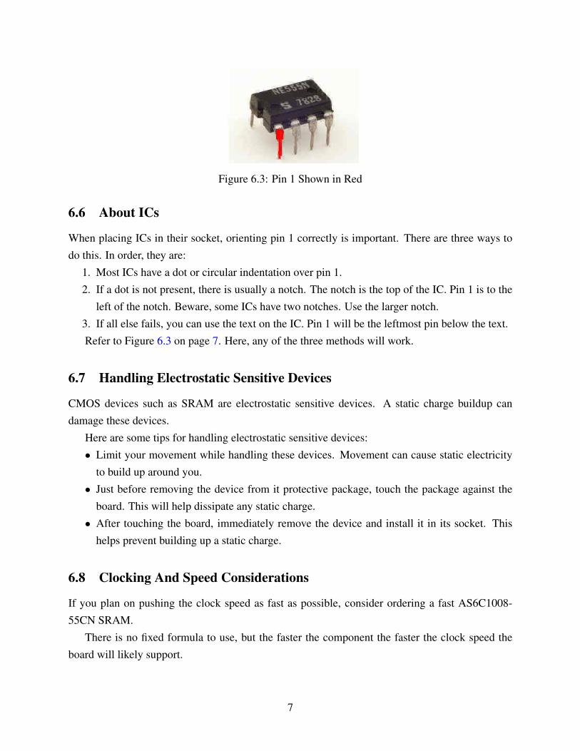
Figure 6.3: Pin 1 Shown in Red
6.6 About ICs
When placing ICs in their socket, orienting pin 1 correctly is important. There are three ways to
do this. In order, they are:
1. Most ICs have a dot or circular indentation over pin 1.
2. If a dot is not present, there is usually a notch. The notch is the top of the IC. Pin 1 is to the
left of the notch. Beware, some ICs have two notches. Use the larger notch.
3. If all else fails, you can use the text on the IC. Pin 1 will be the leftmost pin below the text.
Refer to Figure 6.3 on page 7. Here, any of the three methods will work.
6.7 Handling Electrostatic Sensitive Devices
CMOS devices such as SRAM are electrostatic sensitive devices. A static charge buildup can
damage these devices.
Here are some tips for handling electrostatic sensitive devices:
• Limit your movement while handling these devices. Movement can cause static electricity
to build up around you.
• Just before removing the device from it protective package, touch the package against the
board. This will help dissipate any static charge.
• After touching the board, immediately remove the device and install it in its socket. This
helps prevent building up a static charge.
6.8 Clocking And Speed Considerations
If you plan on pushing the clock speed as fast as possible, consider ordering a fast AS6C1008-
55CN SRAM.
There is no fixed formula to use, but the faster the component the faster the clock speed the
board will likely support.
7

Figure 6.4: Tools
6.9 Tools and Mechanical Considerations
Part mounted in holes on the board must be soldered into place. To avoid cold joints and solder
bridges, a temperature controlled soldering station is highly recommended.
Figure 6.4 on page 8 shows tools frequently used in assembling boards:
6.10 Soldering
Figure 6.5 on page 9 shows how to make a good solder connection. For best results, the soldering
iron should touch both the component lead and board at a 45 angle so that both are properly heated
and will accept the solder. If you notice a buildup of old solder and rosin, you should clean the
soldering iron tip.
This is best done by brushing the tip on a wet sponge using a swiping motion.
Two common soldering problems are cold joints and bridges. A cold joint occurs when the
lead and board are not heated evenly. Figure 6.5 shows the two ways this can happen – either the
soldering iron is placed on the lead or board (but not both).
The other problem is a solder bridge. Figure 6.6 on page 10 shows this. (The H8 8080A/Z80
64K RAM ORG0 V1.3 has a solder mask that helps reduce the chance for a solder bridge.)
8
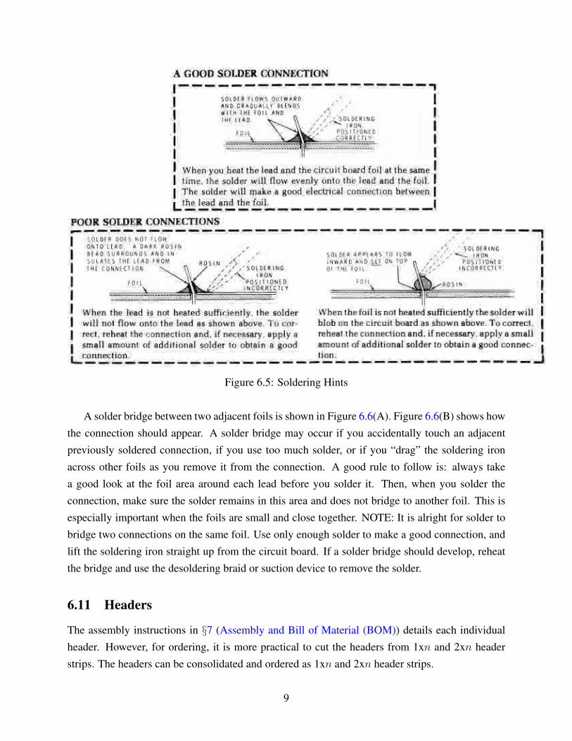
Figure 6.5: Soldering Hints
A solder bridge between two adjacent foils is shown in Figure 6.6(A). Figure 6.6(B) shows how
the connection should appear. A solder bridge may occur if you accidentally touch an adjacent
previously soldered connection, if you use too much solder, or if you “drag” the soldering iron
across other foils as you remove it from the connection. A good rule to follow is: always take
a good look at the foil area around each lead before you solder it. Then, when you solder the
connection, make sure the solder remains in this area and does not bridge to another foil. This is
especially important when the foils are small and close together. NOTE: It is alright for solder to
bridge two connections on the same foil. Use only enough solder to make a good connection, and
lift the soldering iron straight up from the circuit board. If a solder bridge should develop, reheat
the bridge and use the desoldering braid or suction device to remove the solder.
6.11 Headers
The assembly instructions in §7 (Assembly and Bill of Material (BOM)) details each individual
header. However, for ordering, it is more practical to cut the headers from 1xn and 2xn header
strips. The headers can be consolidated and ordered as 1xn and 2xn header strips.
9

Figure 6.6: Solder Bridges
The holes on the board are a tight fit for the headers. The headers can be inserted by gently
rocking the header into the holes while applying downward pressure. Because of the tight fit and
to avoid mechanical interference from other parts, the headers are installed first.
7 Assembly and Bill of Material (BOM)
If you have not read §6 (Getting Ready), at least follow the steps below in order.
This section documents the parts ordering and assembly process. Following the instructions in
sequence helps minimize mechanical interference and assembly errors. Parts are grouped into part
types (e.g., resistors, capacitors, etc.). These form the assembly sections below.
Within each assembly section, parts of that type are listed as bullet items. For each part, the
number of parts required along with a full description of the part are included. Beneath each item,
the locations where that part is used are listed. There is a space on the left to check off each item
as you install it. Note that some parts are optional.
Installing all instances of a part at a time helps reduces assembly errors and eases pulling parts.
The order of assembly helps reduce mechanical problems. As each component is installed, check
it off.
10
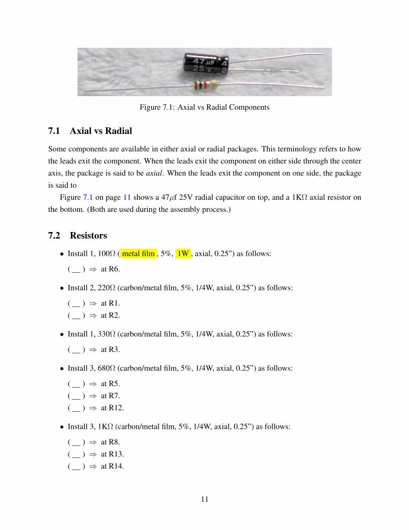
Figure 7.1: Axial vs Radial Components
7.1 Axial vs Radial
Some components are available in either axial or radial packages. This terminology refers to how
the leads exit the component. When the leads exit the component on either side through the center
axis, the package is said to be axial. When the leads exit the component on one side, the package
is said to
Figure 7.1 on page 11 shows a 47µf 25V radial capacitor on top, and a 1KΩ axial resistor on
the bottom. (Both are used during the assembly process.)
7.2 Resistors
• Install 1, 100Ω ( metal film , 5%, 1W , axial, 0.25”) as follows:
( ) ⇒ at R6.
• Install 2, 220Ω (carbon/metal film, 5%, 1/4W, axial, 0.25”) as follows:
( ) ⇒ at R1.
( ) ⇒ at R2.
• Install 1, 330Ω (carbon/metal film, 5%, 1/4W, axial, 0.25”) as follows:
( ) ⇒ at R3.
• Install 3, 680Ω (carbon/metal film, 5%, 1/4W, axial, 0.25”) as follows:
( ) ⇒ at R5.
( ) ⇒ at R7.
( ) ⇒ at R12.
• Install 3, 1KΩ (carbon/metal film, 5%, 1/4W, axial, 0.25”) as follows:
( ) ⇒ at R8.
( ) ⇒ at R13.
( ) ⇒ at R14.
11
• Install 3, 2KΩ (carbon/metal film, 5%, 1/4W, axial, 0.25”) as follows:
( ) ⇒ at R4.
( ) ⇒ at R9.
( ) ⇒ at R10.
7.3 Diodes
• Install 5, 1N5819 (DO-41) as follows:
( ) ⇒ at D3.
( ) ⇒ at D4.
( ) ⇒ at D5.
( ) ⇒ at D6.
( ) ⇒ at D7.
7.4 LEDs
• Install 1, LED (radial, green, 0.1”) (See §5.1 on page 2 for required solder mask rework.)
as follows:
( ) ⇒ D1/POWER-LED.
• Install 1, LED (radial, red, 0.1”) (See §5.1 on page 2 for required solder mask rework.) as
follows:
( ) ⇒ D2/Side-Select.
• Install 1, LED (radial, blue, 0.1”) (See §5.1 on page 2 for required solder mask rework.) as
follows:
( ) ⇒ D8/A16 ENABLED.
7.5 Capacitors
• Install 15, .1µf (ceramic, radial, 0.1”) as follows:
( ) ⇒ at C6.
( ) ⇒ at C7.
( ) ⇒ at C8.
( ) ⇒ at C9.
( ) ⇒ at C10.
12
( ) ⇒ at C11.
( ) ⇒ at C12.
( ) ⇒ at C13.
( ) ⇒ at C14.
( ) ⇒ at C15.
( ) ⇒ at C16.
( ) ⇒ at C17.
( ) ⇒ at C18.
( ) ⇒ at C19.
( ) ⇒ at C21.
7.6 Tantalum Capacitors
• Install 4, 33µf (tantalum, 25V, radial, 0.1”) as follows:
( ) ⇒ at C1.
( ) ⇒ at C2.
( ) ⇒ at C20.
( ) ⇒ at C5.
7.7 Resistor Packs
• Install 2, 1KΩ bussed (SIP-9) as follows:
( ) ⇒ at RR1.
( ) ⇒ at RR2.
7.8 Edge Connectors
• Install 2, 25 Position Receptacle Connector 0.100” right angle gold (Samtec BCS-125-L-S-
HE, Digi-Key SAM1009-25-ND) as follows:
( ) ⇒ at P1.
( ) ⇒ at P2.
7.9 Jumpers
• Install 4, 1x2 Straight Male Pin Header (0.1”, 0.025” square posts) as follows:
( ) ⇒ at JP1.
13
( ) ⇒ at JP2.
( ) ⇒ at JP4.
( ) ⇒ at JP6.
• Install 3, 1x3 Straight Male Pin Header (0.1”, 0.025” square posts) as follows:
( ) ⇒ at JP3.
( ) ⇒ at JP5.
( ) ⇒ at J1.
7.10 Switches
• Install 2, 8 position DIP switch (DIP-16, 0.3”) as follows:
( ) ⇒ at SW1.
( ) ⇒ at SW2.
7.11 Sockets
• Install 6, 14-Pin socket (DIP, 0.3”) as follows:
( ) ⇒ at U1.
( ) ⇒ at U15.
( ) ⇒ at U3.
( ) ⇒ at U5.
( ) ⇒ at U6.
( ) ⇒ at U7.
• Install 1, 16-Pin socket (DIP, 0.3”) as follows:
( ) ⇒ at U12.
• Install 5, 20-Pin socket (DIP, 0.3”) as follows:
( ) ⇒ at U10.
( ) ⇒ at U2.
( ) ⇒ at U4.
( ) ⇒ at U8.
( ) ⇒ at U9.
• Install 1, 32-Pin socket (DIP, 0.6”) as follows:
( ) ⇒ at U16.
14
• Install 1, LIR2032 battery socket as follows:
( ) ⇒ at BT1.
7.12 Integrated Circuits
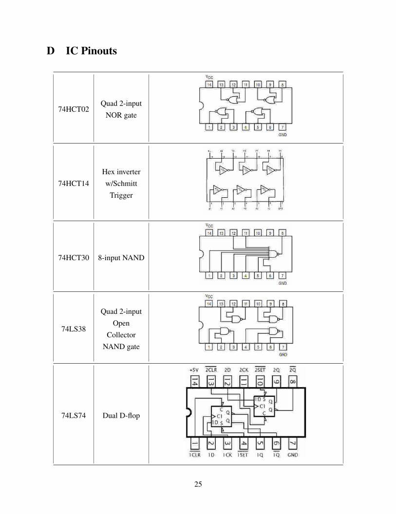
• Install 1, 74HCT/LS02 (Quad 2-input NOR gates, DIP-14, 0.3”) as follows:
( ) ⇒ at U7.
• Install 1, 74HCT/LS14 (Hex inverters w/Schmitt Trigger, DIP-14, 0.3”) as follows:
( ) ⇒ at U1.
• Install 2, 74HCT/LS30 (8-input NAND gate, DIP-14, 0.3”) as follows:
( ) ⇒ at U5.
( ) ⇒ at U15.
• Install 1, 74HCT/LS38 (Quad 2-input Open Collector NAND gates, DIP-14, 0.3”) as fol-
lows:
( ) ⇒ at U6.
• Install 1, 74HCT/LS74 (Dual positive-edge-triggered D flipflops, DIP-14, 0.3”) as follows:
( ) ⇒ at U3.
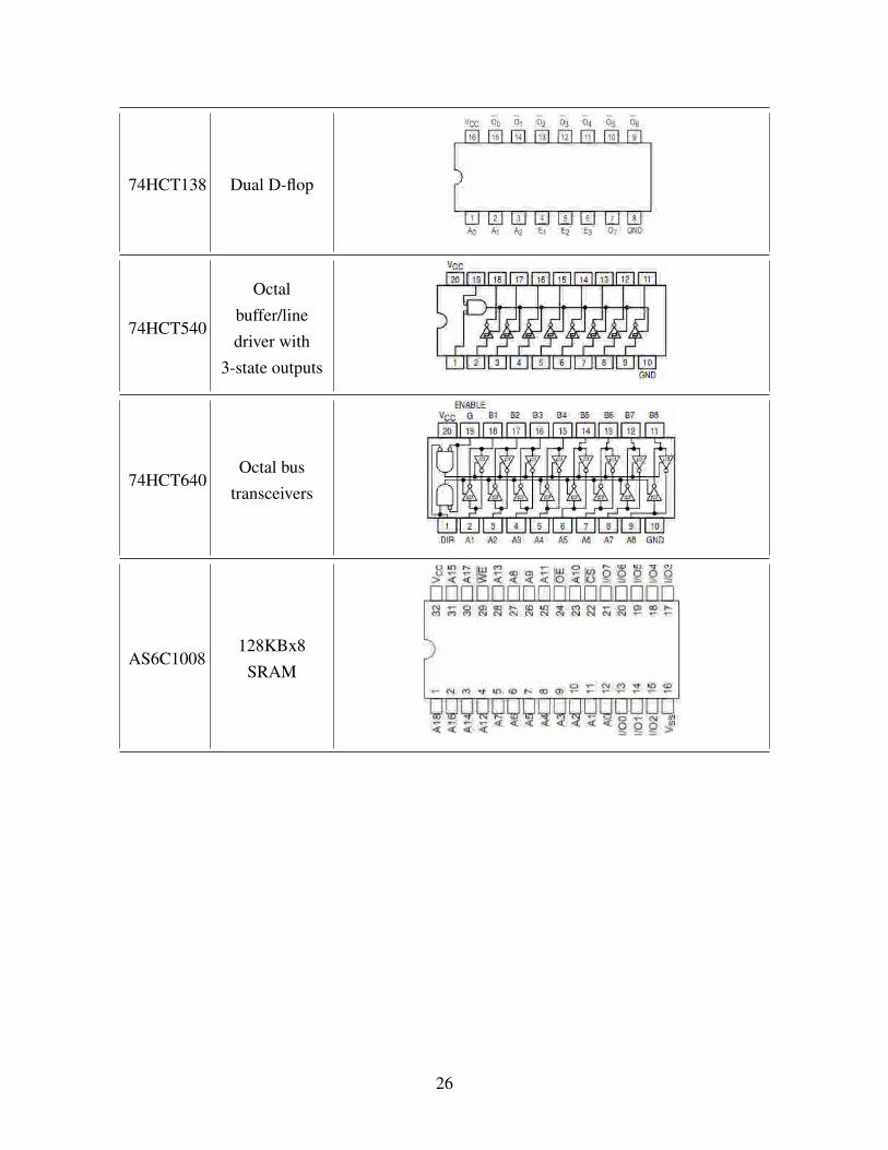
• Install 1, 74HCT/LS138 (3 To 8 Decoder/Demultiplexer, DIP-16, 0.3”) as follows:
( ) ⇒ at U12.
• Install 4, 74HCT/LS540 (Octal buffer/line driver with 3-state outputs, DIP-20, 0.3”) as fol-
lows:
( ) ⇒ at U2.
( ) ⇒ at U4.
( ) ⇒ at U8.
( ) ⇒ at U9.
• Install 1, 74HCT/LS640 (Octal bus transceivers, DIP-20, 0.3”) as follows:
( ) ⇒ at U10.
• Install 1, AS6C1008-55PCN (128Kx8 SRAM, DIP-32, 0.6”) (See §6.7 on page 7 for han-
dling considerations and §6.8 on page 7 for speed considerations.) as follows:
15

( ) ⇒ at U16.
• Install 1, DS1210 (Nonvolatile Controller Chip, DIP-8, 0.3”) (See §?? on page ?? for order-
ing details.) as follows:
( ) ⇒ at U17.
• Install 1, TL7757 (Supply-Voltage Supervisor, TO-92) as follows:
( ) ⇒ at U14.
7.13 Voltage Regulators
• Install 1, 7805 5V Voltage regulator (TO-220) (See §6.5, page 6 for special mounting in-
structions.) (Not used when S7V7F5 is used. See §6.4, page 5.) as follows:
( ) ⇒ at U13.
7.14 Heatsinks
• Install 1, Heatsink (TO-220, compact, 0.5” width) (See §6.5, page 6 for special mounting
instructions.) (Not used when S7V7F5 is used. See §6.4, page 5.) as follows:
( ) ⇒ at U13.
7.15 Battery Cells
• Install 1, LIR2032 Li-ion Rechargeable Button Coin Cell Battery w/Tab (3.6V, 40mAh) as
follows:
( ) ⇒ at BT1.
16

XCON-8/PAM37 MonitorsMemory
BankAddress Range
(Octal)Switch
Position
8K 000-000Q to 037-377Q 1 = ON
16K 040-000Q to 077-377Q 2 = ON
24K 100-000Q to 137-377Q 3 = ON
32K 140-000Q to 177-377Q 4 = ON
40K 200-000Q to 237-377Q 5 = ON
48K 240-000Q to 277-377Q 6 = ON
56K 300-000Q to 337-377Q 7 = ON
64K 340-000Q to 377-377Q 8 = ON
(a) XCON-8/PAM37 Monitors
PAM-8 MonitorMemory
BankAddress Range
(Octal)Switch
Position
0K000-000Q to 037-377Q(Reserved for Monitor) 1 = OFF
8K 040-000Q to 077-377Q 2 = ON
16K 100-000Q to 137-377Q 3 = ON
24K 140-000Q to 177-377Q 4 = ON
32K 200-000Q to 237-377Q 5 = ON
40K 240-000Q to 277-377Q 6 = ON
48K 300-000Q to 337-377Q 7 = ON
56K 340-000Q to 377-377Q 8 = ON
(b) PAM-8 Monitor
Table 7.1: SW2 Settings
8 Configuration
1. Refer to Figure 7.2 on page 18 to set the Extended Configuration 8-position DIP switch at
SW1 (Status Port). Note the numbering on the switch may not match the numbering on the
silkscreen. Always use the number on the silkscreen. Also, the mechanism for closing the
switch varies with the switch. Always use the documentation on the switch to determine the
on/off position.
2. Table 7.1 on page 17 details the address selection switch settings for the PAM/8 and XCON-
8/PAM37 monitors. Set SW2 to the settings appropriate for your monitor. As before, use the
switch numbering on the silkscreen and the on/off position marked on the switch.
3. Jumpers:
• JP1 - “CHARGE”: By default is installed as it is used to charge the battery. Remove
it if the battery is non-rechargeable.
• JP2 - “RBAT (Remove Battery)”: On for normal operation. Removed when replacing
the RAM IC.
17
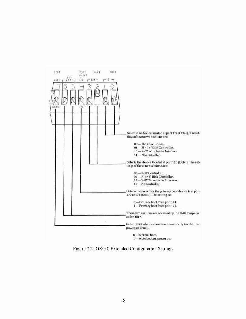
Figure 7.2: ORG 0 Extended Configuration Settings
18

• JP3 - “H8-SS (Side Select)”: Select which backplane pin receives the side select signal
for the H17 controller. Choices are pin #18 or pin #24.
• JP4 - “A16SW (RAM Address A16 Connects to an External Switch)”: External
switch “OFF” for normal operation. When external switch is “ON”, it enables the
second bank of the 64K RAM, so that the user can key-in manually any programs that
they want to preserved. LED D8 turns on when switch is in the “ON” position.
• JP5 - “ORG-DISABLE”: Insert jumper between pins 1-2 for normal operation. Insert
jumper between pins 2-3 to disable the circuit if using the Heath ORG0 card. Please
disable when using Heath/Zenith Z80 or Les Bird’s Z80 CPU board. Please enable for
the 8080 CPU board.
• JP6 - “BRD-DISABLE”: This is useful for bank switching and adding more than 1
board.
• “TP1 BAT”: This the test point. Should be 4.75V when power is on and 4.50V when
power is off.
• “TP2-RESET”: This the test point.
9 Final Assembly
There is a gap between the edge connectors on the right side of the board. On Heathkit boards a
solid nylon spacer is installed in the gap. The spacer ensures the board is aligned properly when
plugged into the backplane. Similar provisions should be made for this board. One easy solution
is to glue a jumper header into gap using Gorilla glue.
The last step is a visual inspection of the board looking for:
• Unsoldered connections
• Cold solder joints
• Solder bridges
• The correct ICs are inserted into their sockets
• The ICs are oriented in their socket correctly and there are no bent pins
• Jumpers are installed correctly
10 Installation
• If the system contains an HA8-8 Extended Configuration Card (commonly known as an
ORG 0 board), remove it.
19
• Install the H8 8080A/Z80 64K RAM ORG0 V1.3 in a backplane the slot behind the CPU
card. Ensure the edge connectors properly align with the backplane pins.
11 Acknowledgements
The author is grateful for the input and assistance of Norberto Collado.
20
Appendices
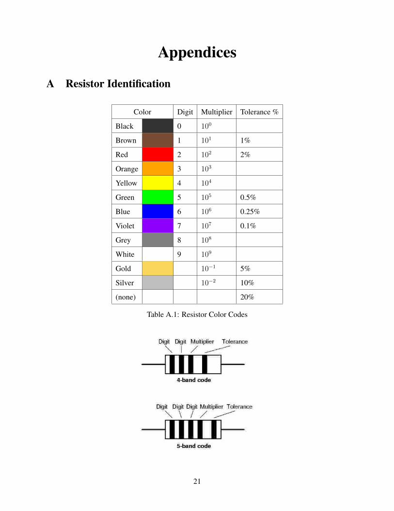
A Resistor Identification
Color Digit Multiplier Tolerance %
Black 0 100
Brown 1 101 1%
Red 2 102 2%
Orange 3 103
Yellow 4 104
Green 5 105 0.5%
Blue 6 106 0.25%
Violet 7 107 0.1%
Grey 8 108
White 9 109
Gold 10−1 5%
Silver 10−2 10%
(none) 20%
Table A.1: Resistor Color Codes
21
Example: The resistor below colored Orange-Orange-Black-Brown-Violet would be 3.3 kΩ
with a tolerance of +/- 0.1%.
B Polarized Devices
A polarized device has positive (anode) and negative (cathode) leads. Polarized devices must be
inserted into the holes that match the lead’s polarity.
On the H8 8080A/Z80 64K RAM ORG0 V1.3 four polarized devices are used: diodes, LEDS,
tantalum capacitors, and electrolytic capacitors.
B.1 Diodes
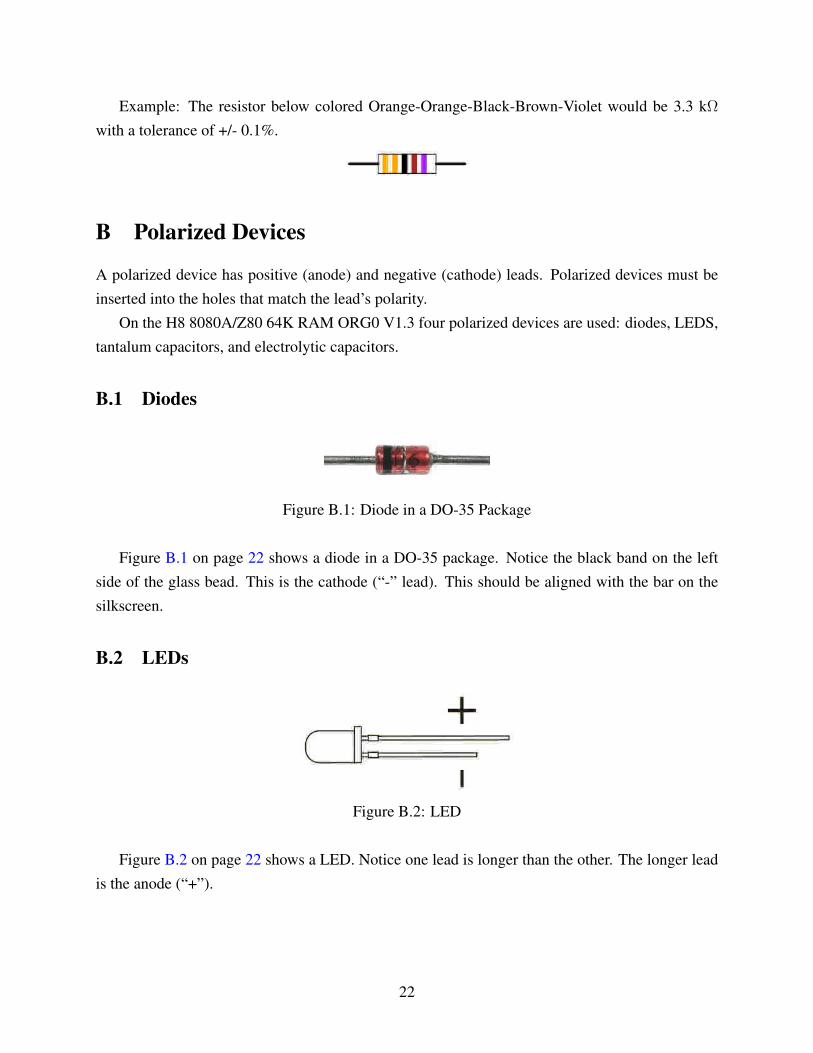
Figure B.1: Diode in a DO-35 Package
Figure B.1 on page 22 shows a diode in a DO-35 package. Notice the black band on the left
side of the glass bead. This is the cathode (“-” lead). This should be aligned with the bar on the
silkscreen.
B.2 LEDs
Figure B.2: LED
Figure B.2 on page 22 shows a LED. Notice one lead is longer than the other. The longer lead
is the anode (“+”).
22

B.3 Tantalum Capacitors
Figure B.3: Tantalum Capacitor
Figure B.3 on page 23 shows a tantalum capacitor. Notice one lead is longer than the other.
The longer lead is the anode (“+”).
23

C Connector Pinouts
C.1 H8 Backplane Connector
24
D IC Pinouts
74HCT02Quad 2-input
NOR gate
74HCT14
Hex inverter
w/Schmitt
Trigger
74HCT30 8-input NAND
74LS38
Quad 2-input
Open
Collector
NAND gate
74LS74 Dual D-flop
25
74HCT138 Dual D-flop
74HCT540
Octal
buffer/line
driver with
3-state outputs
74HCT640Octal bus
transceivers
AS6C1008128KBx8
SRAM
26

27

E Schematic
28


