SPRABV0—March 2014 Hardware Design Guide for KeyStone II Devices Application Report Page 1 of 126Submit Documentation Feedback
SPRABV0—March 2014
Please be aware that an important notice concerning availability, standard warranty, and use in critical applicationsof Texas Instruments semiconductor products and disclaimers thereto appears at the end of this document.
Application Report
Hardware Design Guide for KeyStone II DevicesHigh-Performance and Multicore Processors
AbstractThis document describes hardware system design considerations for the KeyStone II family of processors. This design guide is intended to be used as an aid during the development of application hardware. Other aids including, but not limited to, device data manuals and explicit collateral should also be used.
SPRABV0—March 2014 Hardware Design Guide for KeyStone II Devices Application Report Page 5 of 126Submit Documentation Feedback
www.ti.com
PurposeThis document is intended to aid in the hardware design and implementation of a KeyStone II-based system. This document should be used along with the respective data manual and other relevant user guides and application reports.
TrademarksSmartReflex is a trademark of Texas Instruments.All other trademarks belong to their respective owners.
Terms and Abbreviations
AIF Antenna Interface
AMI IBIS Algorithmic Modeling Interface
BGA Ball Grid Array
CML Current Mode Logic, I/O type
Data Manual Also referred to as the Data Sheet
DDR3 Double Data Rate 3 (SDRAM Memory)
DSP Digital Signal Processor
EMIF External Memory Interface
EVM Evaluation Module
FC-BGA Flip-Chip BGA
GPIO General-Purpose I/O
I2C Inter-IC Control Bus
IBIS Input Output Buffer Information Specification, or ANSI/EIA-656-A
IO Input / Output
JEDEC Joint Electronics Device Engineering Council
Page 6 of 126 Hardware Design Guide for KeyStone II Devices Application Report SPRABV0—March 2014Submit Documentation Feedback
1 Introduction www.ti.com
1 IntroductionThe Hardware Design Guide for KeyStone II Devices Application Report provides a starting point for the engineer designing with one of the KeyStone II devices. It shows a road map for the design effort and highlights areas of significant importance that must be addressed. This document does not contain all the information that is needed to complete the design. In many cases, it refers to the device-specific data manual or to various user guides as sources for specific information.
This guide is generic to the entire family of KeyStone II devices, and as such, may include information for subsystems that are not present on all devices. Designers should begin by reviewing the device-specific data manual for their intended device to determine which sections of this guide are relevant.
The guide is organized in a sequential manner. It moves from decisions that must be made in the initial planning stages of the design, through the selection of support components, to the mechanical, electrical, and thermal requirements. For the greatest success, each of the issues discussed in a section should be resolved before moving to the next section.
1.1 Before Getting StartedThe KeyStone II family of processors provides a wide variety of capabilities, not all of which will be used in every design. Consequently, the requirements for different designs using the same device can vary widely depending on how that part is used. Many designers simply copy the evaluation module (EVM) for the device without determining their requirements. While the EVM is a good example, it is not a reference design and may not be the optimum design for every customer. You will need to understand your requirements before determining the details of the design. In addition, your design may require additional circuitry to operate correctly in the target environment. Take some time to review the data manual for your KeyStone II device and determine the following:
• Which peripherals will be used to move data in and out of the processor• What is the speed and organization of the DDR3 memory interface that will be
used• How much processing will each of the cores in your KeyStone II device be
performing• How you will boot the KeyStone II device• What are the expected environmental conditions for your KeyStone II device
1.2 Design DocumentationThroughout this guide, we will periodically recommend that a design document be generated based on your requirements. Generating and storing this information will provide you with the foundation for your documentation package and this design document will be needed if you are seeking support from TI. Examples of many of these can be found in the schematic package provided with the EVM boards for your KeyStone II device.
SPRABV0—March 2014 Hardware Design Guide for KeyStone II Devices Application Report Page 7 of 126Submit Documentation Feedback
2 Power Supplieswww.ti.com
2 Power SuppliesThe first requirement for a successful design is to determine the power needs for your KeyStone device. All KeyStone II devices operate with six main voltage levels requiring six power supply circuits. Some devices will require an additional voltage level, requiring a seventh power supply. Check the device-specific data manual to determine all the voltages needed.
2.1 Determining Your Power RequirementsThe maximum and minimum current requirements for each of these voltage rails are not found in the data manual for the part. These requirements are highly application-dependent and must be calculated for your specific product. There is a power consumption model in the product folder for each KeyStone II device. You must use the model for the specific KeyStone II device that you have selected to get accurate results.
There is a link in the model spreadsheet to an application note that explains how to populate the necessary parameters. Review this application note carefully and determine the values needed for your application. Once you have entered these values you will have the maximum power requirement for each of the six voltage rails. These values are divided into activity and baseline components. The baseline power portion is associated with leakage, clock tree, and phase-locked loop (PLL) power. This value will not change based on the processor utilization. The activity power reflects the additional power required due to the processing load defined in the spreadsheet. The baseline plus the activity defines your maximum power requirement. Power supplies should be designed to transition from the baseline level to the baseline + activity level within one CPU clock.
Note that power consumption can vary greatly based on process and temperature. The values provided by the spreadsheet are the maximum average power consumption for all production devices. Measurements of power consumption on a single device may be considerably lower than the values provided by the model, but may not be representative of a wide sample of devices. To ensure that your power supply design is adequate, use the values provided by the model.
The power consumption model populated with the values for your application should be saved with your design documentation.
SPRABV0—March 2014 Hardware Design Guide for KeyStone II Devices Application Report Page 9 of 126Submit Documentation Feedback
2 Power Supplieswww.ti.com
These six rails (CVDD, CVDD1, 0.85 V, 3.3 V, 1.8 V, and 1.5 V) provide the basic power requirement for all KeyStone II devices. In addition, each requires a number of filtered connections to the main rails to provide power for noise-sensitive portions of the device. These include the VDDAHV, VDDALV, and AVDDAn pins. The power requirements for each of the filtered voltages are included in the values calculated by the power consumption models.
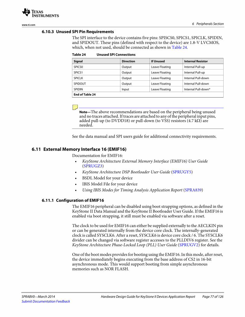
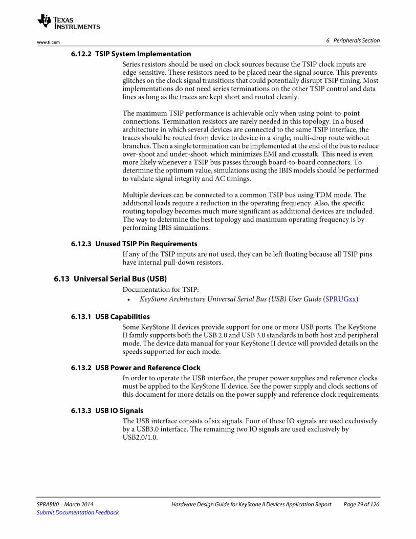
KeyStone II devices have power pins specifically for the USB interface. These include VDDUSB, VP0:1, VPTX0:1, VPH0:1, and DVDD33_0:1. These pins need to be supplied only if the USB interface is used in your design.
Figure 1 also includes a DDR3 termination power supply. DDR3 address and command signals are terminated using a source/sink-tracking LDO designed to provide VTT and a low-noise reference. Figure 1 includes this power supply as a source for the VREFSSTL reference voltage.
Each of these voltage rails and filtered supplies are described in the following sections.
2.2.1 CVDDCVDD is the adjustable supply used by the core logic for the KeyStone II device. KeyStone II devices use adaptive voltage scaling (AVS) to compensate for variations in performance from die to die, and from wafer to wafer. The actual voltage for CVDD can vary across the range specified in the device data manual and will be different for each component. Each KeyStone II device needs an independent power supply to generate the CVDD voltage needed by that device. That CVDD power supply must use a SmartReflex-compliant circuit. SmartReflex is described in the next section. This power supply circuit must initialize to a level of 1.0 V and then adjust to the voltage requested by the SmartReflex circuit in the KeyStone II device.
2.2.1.1 SmartReflexTo reduce device power consumption, SmartReflex allows the core voltage to be optimized (scaled) based on the process corners of each device. KeyStone II devices use Class 0 SmartReflex. This class of operation uses a code for a single ideal voltage level determined during manufacturing tests. At the end of these tests, the code for the lowest acceptable voltage (while still meeting all performance requirements) is established and permanently programmed into each die. This 6-bit code, referred to as the VID value, represents the optimal fixed voltage level for that device.
Page 10 of 126 Hardware Design Guide for KeyStone II Devices Application Report SPRABV0—March 2014Submit Documentation Feedback
2 Power Supplies www.ti.com
Table 1 shows the voltage level associated with each of the possible 6-bit VID values.
Note—Not all ranges or voltage levels are supported by every KeyStone II device. The intended range of operation is defined in the device-specific data manual. Operation outside that range may impact device reliability or performance.
2.2.1.2 SmartReflex VCNTL InterfaceThe VCNTL[5:0] interface is used to transmit the 6-bit VID value to the SmartReflex power supply circuit. The VCNTL[5:0] pins are open-drain IOs, and require 4.7-k pull-up resistors to the DVDD18 rail of the KeyStone II device. VCNTL[5:0] can support either a 6-pin, 6-bit single-phase interface or a 4-pin 6-bit dual-phase interface for transmitting the 6-bit VID value. The later is compatible with KeyStone I devices. The mode is selected using the AVSIFSEL[1:0] configuration pins. Note that the other two modes listed in the data manual are for future enhancements and are not currently supported. In 6-pin, 6-bit single phase mode, the 6-bit VID value is driven out using all six VCNTL pins once the POR is released. All six bits will change at approximately the same time to indicate the new value of the AVS voltage. In 4-pin, 6-bit dual-phase mode, VCNTL[5] acts as a command signal while VCNTL[4:2] acts as a 3-bit data bus. VCNTL[5] will transition low and then high to indicate the presence of the lower three bits of the VID value, followed by the upper three bits.
Table 1 SmartReflex VID Value Mapping
VID # VID (5:0) CVDD VID # VID (5:0) CVDD VID # VID (5:0) CVDD VID # VID (5:0) CVDD
SPRABV0—March 2014 Hardware Design Guide for KeyStone II Devices Application Report Page 11 of 126Submit Documentation Feedback
2 Power Supplieswww.ti.com
The timing of this interface can be found in the data manual for your KeyStone II device. It is important to note that the VID values are not latched on the falling and rising edge of the VCNTL[5] signal. The VID values will be available only after a specified amount of time following the transition, as defined in the data manual for the KeyStone II device. As stated previously, this transition will occur only a single time after a power-up reset has occurred. The connection of the VCNTL interface to the power supply circuit is discussed in later sections.
2.2.1.3 Supported Power Supply SolutionsTexas Instruments provides a number of power supply solutions for CVDD, which fall into one of two classes. The first uses the LM10011 to interface the VCNTL pins with a number of analog power supply controllers. The second is a solution based on the UCD92xx family of digital power supply controllers.
Texas Instruments provides reference designs for both possible power supply solutions. These can be accessed through the power management page on TI.com:
http://www.ti.com/processorpower
Choose C6000 from the processor type pull down menu and then choose the KeyStone II part number from the processor family pull down menu. This will bring you to a page containing the documentation for the possible power supply solutions that are supported for that part. The page will include power supply requirements. These are generally the requirements calculated for the EVM platform and do not reflect the maximum requirements for the part. Your requirements should be calculated using the Power Consumption Model for your KeyStone II device.
The power management solutions are managed by a different group in TI. Questions on the power supply solutions should be directed to the appropriate power group. Questions about the LM10011-based solution can be posted to the non-isolated DC/DC forum and questions about the UCD92xx based solutions can be posted to the Digital Power Forum. If you need additional information, contact your local Texas Instruments FAE.
2.2.1.4 LM10011 and Analog Controller SolutionsThe LM10011 captures the VID value presented on the VCNTL interface and uses it to control the voltage level of a DC/DC converter. The VID value is used to define the output of a current DAC that is connected to the feedback pin of a DC/DC switching regulator. This will adjust the output voltage of the regulator to the level required by the KeyStone II device. The LM10011 can be used to control any DC/DC regulator with a compatible feedback circuit. The current requirements calculated using the power consumption model should be used to determine the best device for your application.
An example design using the TPS56121 can be found at the following link.http://www.ti.com/tool/pmp7256
SPRABV0—March 2014 Hardware Design Guide for KeyStone II Devices Application Report Page 13 of 126Submit Documentation Feedback
2 Power Supplieswww.ti.com
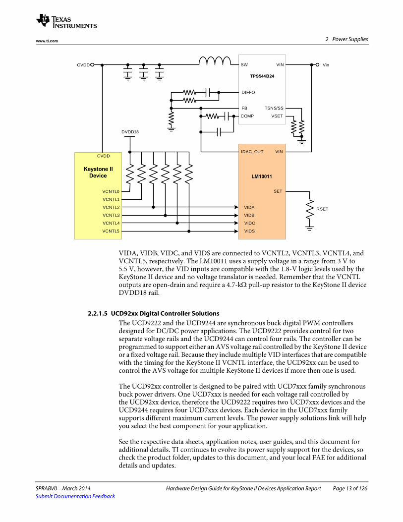
VIDA, VIDB, VIDC, and VIDS are connected to VCNTL2, VCNTL3, VCNTL4, and VCNTL5, respectively. The LM10011 uses a supply voltage in a range from 3 V to 5.5 V, however, the VID inputs are compatible with the 1.8-V logic levels used by the KeyStone II device and no voltage translator is needed. Remember that the VCNTL outputs are open-drain and require a 4.7-k pull-up resistor to the KeyStone II device DVDD18 rail.
2.2.1.5 UCD92xx Digital Controller SolutionsThe UCD9222 and the UCD9244 are synchronous buck digital PWM controllers designed for DC/DC power applications. The UCD9222 provides control for two separate voltage rails and the UCD9244 can control four rails. The controller can be programmed to support either an AVS voltage rail controlled by the KeyStone II device or a fixed voltage rail. Because they include multiple VID interfaces that are compatible with the timing for the KeyStone II VCNTL interface, the UCD92xx can be used to control the AVS voltage for multiple KeyStone II devices if more then one is used.
The UCD92xx controller is designed to be paired with UCD7xxx family synchronous buck power drivers. One UCD7xxx is needed for each voltage rail controlled by the UCD92xx device, therefore the UCD9222 requires two UCD7xxx devices and the UCD9244 requires four UCD7xxx devices. Each device in the UCD7xxx family supports different maximum current levels. The power supply solutions link will help you select the best component for your application.
See the respective data sheets, application notes, user guides, and this document for additional details. TI continues to evolve its power supply support for the devices, so check the product folder, updates to this document, and your local FAE for additional details and updates.
Page 14 of 126 Hardware Design Guide for KeyStone II Devices Application Report SPRABV0—March 2014Submit Documentation Feedback
2 Power Supplies www.ti.com
The UCD92xx components are highly programmable, allowing you to optimize the operation of your supply using the Fusion Digital Power Designer software. The software may be downloaded from: http://focus.ti.com/docs/toolsw/folders/print/fusion_digital_power_designer.html
This Windows-based graphical user interface allows the designer to configure the system operating parameters and store the configuration into non-volatile memory. Examples of the XML configuration files for the KeyStone II device EVMs can be found in the technical documents section for the EVM. Note that these files are specific to the EVM design and will require modifications depending upon the components selected. Communication between the Fusion software and the UCD92xx is achieved using a three-wire PMBUS interface. A connector for this interface should be included in your design to allow programming and monitoring of the operation of the UCD92xx. The Fusion software uses a USB-to-GPIO evaluation pod to facilitate this communication.
Information for this pod can be found at:http://www.ti.com/tool/usb-to-gpio
2.2.1.5.1 KeyStone II/UCD92xx Communications
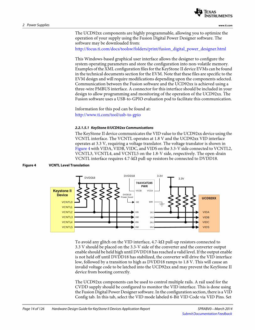
The KeyStone II device communicates the VID value to the UCD92xx device using the VCNTL interface. The VCNTL operates at 1.8 V and the UCD92xx VID interface operates at 3.3 V, requiring a voltage translator. The voltage translator is shown in Figure 4 with VIDA, VIDB, VIDC, and VIDS on the 3.3-V side connected to VCNTL2, VCNTL3, VCNTL4, and VCNTL5 on the 1.8-V side, respectively. The open-drain VCNTL interface requires 4.7-k pull-up resistors be connected to DVDD18.
Figure 4 VCNTL Level Translation
To avoid any glitch on the VID interface, 4.7-k pull-up resistors connected to 3.3 V should be placed on the 3.3-V side of the converter and the converter output enable should be held high until DVDD18 has reached a valid level. If the output enable is not held off until DVDD18 has stabilized, the converter will drive the VID interface low, followed by a transition to high as DVDD18 ramps to 1.8 V. This will cause an invalid voltage code to be latched into the UCD92xx and may prevent the KeyStone II device from booting correctly.
The UCD92xx components can be used to control multiple rails. A rail used for the CVDD supply should be configured to monitor the VID interface. This is done using the Fusion Digital Power Designer software. In the configuration section, there is a VID Config tab. In this tab, select the VID mode labeled 6-Bit VID Code via VID Pins. Set
SPRABV0—March 2014 Hardware Design Guide for KeyStone II Devices Application Report Page 15 of 126Submit Documentation Feedback
2 Power Supplieswww.ti.com
the VID Vout Low to 0.7 V and the VID Vout High to 1.103 V. Note that this defines the full range of VID values shown in Table 1 in this document and not the CVDD voltage range of the KeyStone device as defined in the data manual. These values must be used to ensure that the correct voltage is presented for the VID code received. Set the VID Code Init value to 47, which will provide an initial voltage of1.001V. This voltage will be generated until the KeyStone II device presents the required VID value on the VCNTL interface.
2.2.1.6 CVDD for Designs with Multiple KeyStone II DevicesAs stated previously, each KeyStone II device must have a separate power supply voltage for CVDD even if there are multiple KeyStone II devices on the same board. If a single device is used, then the LM10011-based solution or the UCD9222 can be used. The UCD9222 is a dual controller but the other digital controller in the device can be used to generate one of the other voltages needed by the KeyStone II device. If your design includes multiple KeyStone II devices, you have the option of using any of the recommended power supply designs. A single UCD9222 has two independent VID interfaces and can be used to generate the CVDD voltage for two separate KeyStone II devices. The UCD9244 includes four VID interfaces and can be used for up to four KeyStone II devices.
2.2.2 CVDD1CVDD1 is the fixed 0.95-V supply for the internal memory arrays. This supply must meet the requirements for stability specified in the data manual. This supply cannot be connected to the AVS supply used for CVDD and must be generated by a separate power circuit. If multiple KeyStone II devices are used in your design, a single CVDD1 supply may be used for all of the devices as long as it is scaled to provide the current needed.
2.2.3 CVDDT1Some KeyStone II devices include pins labeled CVDDT1. CVDDT1 is the fixed 0.95-V supply for the internal memory arrays specific to the ARM core. These pins may be connected to the CVDD1 supply and do not need a separate power supply. Be sure to include the current requirements for CVDDT1 when calculating the power for your CVDD1 supply.
2.2.4 DVDD18DVDD18 is the 1.8-V supply for the LVCMOS buffers and for the PLLs. This supply must meet the requirements for stability specified in the data manual. If multiple KeyStone II devices are used in your design, a single 1.8-V supply may be used for all of the devices as long as it is scaled to provide the current needed.
2.2.4.1 AVDDAnThe AVDDA pins provide the supply voltage for the PLL modules in the KeyStone II device. The number of AVDDA pins will vary from device to device depending on the number of PLLs present. Each AVDDA pin should be connected to DVDD18 through a filter circuit. Some of the AVDDAn pins are used as supplies for the DDR3 module DDLs. PLL supply pins must be individually filtered but DLL supply pins for a DDR3 module can be grouped. Check the data manual for your KeyStone II device to determine which AVDDAn pins are PLL supply pins and which are DLL supply pins. For details on the filters, see section 2.3 ‘‘Power Supply Filters’’ on page 19. Note that
Page 16 of 126 Hardware Design Guide for KeyStone II Devices Application Report SPRABV0—March 2014Submit Documentation Feedback
2 Power Supplies www.ti.com
the power estimate generated by the power consumption model includes the power for the AVDDA pins in the total for DVDD18. A current limit value of 50 mA can be used as for each AVDDA pin when selecting filter components. Recommendations for the filter can be found later in this document.
2.2.5 DVDD15DVDD15 is the 1.5-V supply for the DDR3 IO buffers in the KeyStone II device. This supply must meet the requirements for stability specified in the data manual. If multiple KeyStone II devices are used in your design, a single 1.5-V supply may be used for all of the devices as long as it is scaled to provide the current needed.
2.2.6 VDDAHVVDDAHV is an analog supply voltage for the SerDes interfaces in the device and should be filtered from a fixed 1.8-V supply. This supply must meet the requirements for stability specified in the data manual. If multiple KeyStone II devices are used in your design, a single 1.8-V supply may be used for all of the devices as long as it is scaled to provide the current needed, but each SoC should have a separate filter specific to the VDDAHV pins on that device. For details on the filter, see 2.3 ‘‘Power Supply Filters’’ on page 19
2.2.7 VDDALVVDDALV is an analog supply voltage for the SerDes interfaces in the device and should be filtered from a fixed 0.85-V supply. This supply must meet the requirements for stability specified in the data manual. If multiple KeyStone II devices are used in your design, a single 0.85-V supply may be used for all of the devices as long as it is scaled to provide the current needed, but each SoC should have a separate filter specific to the VDDALV pins on that device. For details on the filter, see 2.3 ‘‘Power Supply Filters’’ on page 19
2.2.8 USB Power SuppliesKeyStone II devices have power supply pins that are specific to the USB interface. If the USB interface is not present or is not connected in the customer design, these pins may be connected to ground or left floating. This is true only for the USB supplies listed in this section. All other supplies must be present at all times.
2.2.8.1 VDDUSBxThe VDDUSB is a 0.85-V supply voltage for the digital portion for the USB subsystem. These pins may be connected directly to the 0.85-V supply without any filtering. The 0.85-V supply must meet all stability and noise requirements for the VDDUSBx power rail as specified in the data manual. There is one VDDUSB pin for each USB present in the device.
2.2.8.2 VPxThe VP is a 0.85-V supply voltage for the digital portion for the USB subsystem. These pins must be connected to the 0.85-V supply through a filter. For details on the filter, see 2.3 ‘‘Power Supply Filters’’ on page 19. The VP and VPTX supply pins may be connected to the 0.85-V supply through the same filter. If the device has multiple USB ports, VP0/VPTX0 and VP1/VPTX1 should be filtered separately.
SPRABV0—March 2014 Hardware Design Guide for KeyStone II Devices Application Report Page 17 of 126Submit Documentation Feedback
2 Power Supplieswww.ti.com
2.2.8.3 VPTXxThe VPTX is a 0.85-V supply voltage for the transmitter portion for the USB subsystem. These pins must be connected to the 0.85-V supply through a filter. For details on the filter, see 2.3 ‘‘Power Supply Filters’’ on page 19. The VP and VPTX supply pins may be connected to the 0.85-V supply through the same filter. If the device has multiple USB ports VP0/VPTX0 and VP1/VPTX1 should be filtered separately.
2.2.8.4 DVDD33The DVDD33 is a 3.3-V supply voltage for the high speed portion for the USB subsystem. These pins must be connected to the 3.3-V supply through a filter. For details on the filter, see 2.3 ‘‘Power Supply Filters’’ on page 19. The DVDD33 and VPH supply pins may be connected to the 3.3-V supply through the same filter. If the device has multiple USB ports DVDD33_0/VPH0 and DVDD33_1/VPH1 should be filtered separately.
2.2.8.5 VPHThe VPH is a 3.3-V supply voltage for the super speed portion for the USB subsystem. These pins must be connected to the 3.3-V supply through a filter. For details on the filter, see 2.3 ‘‘Power Supply Filters’’ on page 19. The DVDD33 and VPH supply pins may be connected to the 3.3-V supply through the same filter. If the device has multiple USB ports DVDD33_0/VPH0 and DVDD33_1/VPH1 should be filtered separately.
2.2.9 Other SuppliesThe six supplies listed above provide the majority of the power required for KeyStone II devices, however, your design may require additional supplies. Information for these supplies is provided here to advise the designer of their necessity.
2.2.9.1 VTT Termination SupplyThe DDR3 interface requires a VTT termination at the end of the fly-by chain for the DDR3 address and control signals. The 0.75-V termination voltage is generated using a special push/pull termination regulator specifically designed to meet the VTT requirements for DDR3. The Texas Instruments TPS51200 is one device that meets these requirements. Although the VTT supply is not connected to the KeyStone II devices, it is necessary for the DDR3 interface connected to the device.
Page 18 of 126 Hardware Design Guide for KeyStone II Devices Application Report SPRABV0—March 2014Submit Documentation Feedback
2 Power Supplies www.ti.com
2.2.9.2 VREF SupplyThe KeyStone II device requires a 0.75-V reference voltage connected to the VREFSSTL pin for the DDR3 SDRAM interface. Many VTT termination supplies will provide a separate supply output pin specifically for a reference voltage. This is true for the TPS51200, which provides the reference voltage on the REFOUT pin. If the reference voltage is provided by the VTT termination supply, it should be connected to the VREFSSTL pin. If it is not supplied, a simple voltage divider as shown in Figure 5 can be used. Figure 5 DDR3 VREFSSTL Voltage Divider
All resistive components must be 1% or better tolerance. The VREFSSTL voltage created by the voltage divider should be routed to the KeyStone II device and the memory components using a trace width of 20 mil or greater. Additional bypass capacitors should be placed next to the connections at the KeyStone II device and the memories.
If a resistor divider is used, the VREFSSTL source voltage MUST be generated from the DVDD15. VTT is susceptible to large amounts of switching noise, so never connect the VREFSSTL to the VTT voltage rail.
2.2.9.3 VPPSome KeyStone II devices include a VPP voltage rail. For unsecure devices, the VPP pin should be left unconnected. See the Security Addendum for KeyStone II Devices for information on connecting VPP in designs using secure devices.
SPRABV0—March 2014 Hardware Design Guide for KeyStone II Devices Application Report Page 19 of 126Submit Documentation Feedback
2 Power Supplieswww.ti.com
2.3 Power Supply FiltersThe following section defines the recommended power plane filters for the KeyStone II devices as well as the implementation details and requirements.
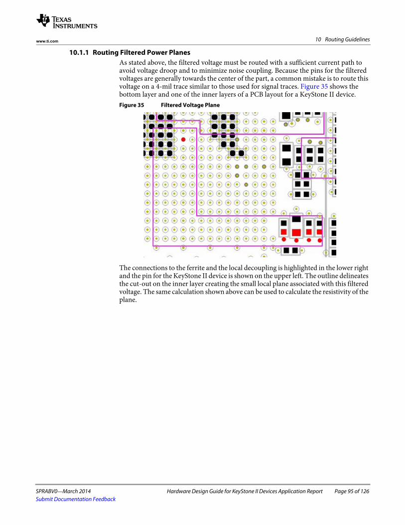
Filters are recommended for the AVDDAn, VDDAHV, VDDALV, VP, VPTX, VPH and DVDD33 voltage rails on the device. An overview of the recommended power supply generation architecture is shown in Figure 6 (only AVDDAn supply rails are shown).
2.3.1 Filters Versus Ferrite BeadsIn previous devices, EMI filters (commonly referred to as T-filters) have been used to condition power rails that may be susceptible to induced noise. These filters acted as low-pass, band-pass, or high-pass filters (depending on selection), limiting parasitic coupled noise on each respective power plane/supply. These EMI filters solve many problems typically overlooked by designers, which may result in device-related problems on production boards.
Ferrite beads also were evaluated based on performance, physical form factor, and cost. Ferrite beads did offer a similar benefit at a lower cost point, and therefore are required by TI for the PLL supplies. See Table 2 for recommended ferrite beads. Key to selecting the EMI filter and ferrite beads are cutoff frequency and current rating.
Table 2 shows the characteristics necessary for selecting the proper noise suppression filter. The following specifications must be adhered to for proper functionality. See the power supply bulk and decoupling capacitor section for additional details necessary to design an acceptable power supply system.
Table 2 Power Rail Filter Recommendations
Power Rail Voltage Filter (p/n) Mfg Current Insertion Loss (dB)/ Impedance Capacitance/DCR
AVDDAn* (PLL) 1.8 BLM15AG121SN1 Murata 200 mA 120 +/- 25% @ 100 MHz** 200 m or less
AVDDAn* (DLL) 1.8 BLM18EG101TN1 Murata 1000 mA 140 +/- 25% @ 100 MHz** 50 m or less
VDDAHV* 1.8 BLM18EG101TN1 Murata 1000 mA 140 +/- 25% @ 100 MHz** 50 m or less
VDDALV* 0.85 BLM18EG101TN1 Murata 1000 mA 14+/- 25% @ 100 MHz** 50 m or less
VP/VPTX* 0.85 BLM18EG101TN1 Murata 1000 mA 14+/- 25% @ 100 MHz** 50 m or less
DVDD33/VPH* 3.3 BLM18EG101TN1 Murata 1000 mA 14+/- 25% @ 100 MHz** 50 m or less
End of Table 2
Note *: Filter not required if peripheral not used. Note **: Requires the addition of a 100-nF and 10-nF ceramic capacitor between the ferrite and respective device pins. Routing must be kept short and clean.
Page 20 of 126 Hardware Design Guide for KeyStone II Devices Application Report SPRABV0—March 2014Submit Documentation Feedback
2 Power Supplies www.ti.com
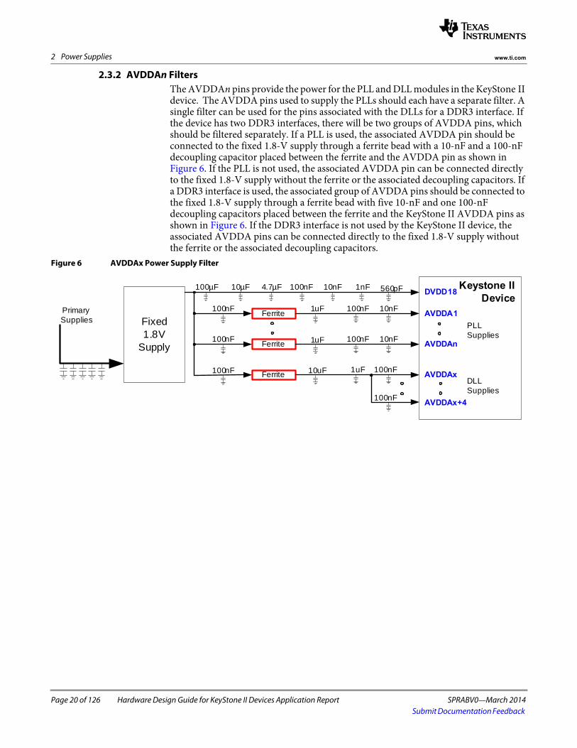
2.3.2 AVDDAn FiltersThe AVDDAn pins provide the power for the PLL and DLL modules in the KeyStone II device. The AVDDA pins used to supply the PLLs should each have a separate filter. A single filter can be used for the pins associated with the DLLs for a DDR3 interface. If the device has two DDR3 interfaces, there will be two groups of AVDDA pins, which should be filtered separately. If a PLL is used, the associated AVDDA pin should be connected to the fixed 1.8-V supply through a ferrite bead with a 10-nF and a 100-nF decoupling capacitor placed between the ferrite and the AVDDA pin as shown in Figure 6. If the PLL is not used, the associated AVDDA pin can be connected directly to the fixed 1.8-V supply without the ferrite or the associated decoupling capacitors. If a DDR3 interface is used, the associated group of AVDDA pins should be connected to the fixed 1.8-V supply through a ferrite bead with five 10-nF and one 100-nF decoupling capacitors placed between the ferrite and the KeyStone II AVDDA pins as shown in Figure 6. If the DDR3 interface is not used by the KeyStone II device, the associated AVDDA pins can be connected directly to the fixed 1.8-V supply without the ferrite or the associated decoupling capacitors.
Page 22 of 126 Hardware Design Guide for KeyStone II Devices Application Report SPRABV0—March 2014Submit Documentation Feedback
2 Power Supplies www.ti.com
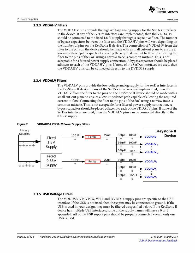
2.3.3 VDDAHV FiltersThe VDDAHV pins provide the high-voltage analog supply for the SerDes interfaces in the device. If any of the SerDes interfaces are implemented, then the VDDAHV should be connected to the fixed 1.8-V supply through a capacitive filter. The number of bypass capacitors between the filter and the VDDAHV pins will vary depending on the number of pins on the KeyStone II device. The connection of VDDAHV from the filter to the pins on the device should be made with a small cut-out plane to ensure a low-impedance path capable of allowing the required current to flow. Connecting the filter to the pins of the SoC using a narrow trace is common mistake. This is not acceptable for a filtered power supply connection. A bypass capacitor should be placed adjacent to each of the VDDAHV pins. If none of the SerDes interfaces are used, then the VDDAHV pins can be connected directly to the DVDD18 supply.
2.3.4 VDDALV FiltersThe VDDALV pins provide the low-voltage analog supply for the SerDes interfaces in the KeyStone II device. If any of the SerDes interfaces are implemented, then the VDDALV from the filter to the pins on the KeyStone II device should be made with a small cut-out plane to ensure a low-impedance path capable of allowing the required current to flow. Connecting the filter to the pins of the SoC using a narrow trace is common mistake. This is not acceptable for a filtered power supply connection. A bypass capacitor should be placed adjacent to each of the VDDALV pins. If none of the SerDes interfaces are used, then the VDDALV pins can be connected directly to the 0.85-V supply.
Figure 7 VDDAHV & VDDALV Power Supply Filters
2.3.5 USB Voltage FiltersThe VDDUSB, VP, VPTX, VPH, and DVDD33 supply pins are specific to the USB interface. If the USB is not used, then these pins may be connected to ground. If the USB is used in your design, they must be filtered as specified below. If the KeyStone II device has multiple USB interfaces, some of the supply names will have a 0 or 1 appended. All of the USB supply pins should be properly connected even if only one USB is used.
SPRABV0—March 2014 Hardware Design Guide for KeyStone II Devices Application Report Page 23 of 126Submit Documentation Feedback
2 Power Supplieswww.ti.com
2.3.5.1 VDDUSB FiltersThe VDDUSB pins provide the logic voltage for the USB interfaces in the KeyStone II device. If any of the USB interfaces are implemented, then the VDDUSB should be connected to the fixed 0.85-V supply through a capacitive filter. The number of bypass capacitors between the filter and the VDDUSB pins will vary depending on the number of pins on the KeyStone II device. The connection of VDDUSB from the filter to the pins on the KeyStone II device should be made with a small cut-out plane to ensure a low-impedance path capable of allowing the required current to flow. Connecting the filter to the pins of the SoC using a narrow trace is common mistake. This is not acceptable for a filtered power supply connection. A bypass capacitor should be placed adjacent to each of the VDDUSB pins.
2.3.5.2 VP & VPTX FiltersThe VP and VPTX pins provide the low analog voltage for the USB interfaces in the device. If any of the USB interfaces are implemented, then both the VP and VPTX pins should be connected to the fixed 0.85-V supply through a capacitive filter. The number of bypass capacitors between the filter and the VP and VPTX pins will vary depending on the number of pins on the KeyStone II device. The connection of VP and VPTX from the filter to the pins on the KeyStone II device should be made with a small cut-out plane to ensure a low-impedance path capable of allowing the required current to flow. Connecting the filter to the pins of the SoC using a narrow trace is common mistake. This is not acceptable for a filtered power supply connection. A bypass capacitor should be placed adjacent to each of the VP and VPTX pins.
2.3.5.3 VPH & DVDD33 FiltersThe VPH and DVDD33 pins provide the high analog voltage for the USB interfaces in the KeyStone II device. If any of the USB interfaces are implemented, then both the VPH and DVDD33 pins should be connected to the fixed 3.3-V supply through a capacitive filter. The number of bypass capacitors between the filter and the VPH and DVDD33 pins will vary depending on the number of pins on the KeyStone II device. The connection of VPH and DVDD33 from the filter to the pins on the KeyStone II device should be made with a small cut-out plane to ensure a low-impedance path capable of allowing the required current to flow. Connecting the filter to the pins of the SoC using a narrow trace is common mistake. This is not acceptable for a filtered power supply connection. A bypass capacitor should be placed adjacent to each of the VP and VPTX pins.
Page 24 of 126 Hardware Design Guide for KeyStone II Devices Application Report SPRABV0—March 2014Submit Documentation Feedback
2 Power Supplies www.ti.com
2.4 Power-Supply Decoupling and Bulk CapacitorsTo properly decouple the supply planes from system noise, decoupling and bulk capacitors are required. Component parasitics play an important role on how well noise is decoupled. For this reason, bulk capacitors should be of the low ESR/ESL type and all decoupling capacitors (unless otherwise specified) should be ceramic and 0402 size (largest recommended). As always, power rating and component and PCB parasitics must be taken into account when developing a successful power supply system. Proper board design and layout allow for correct placement of all capacitors (see the reference table in Section 2.4.4 for a minimum set of capacitor recommendations and values).
Bulk capacitors are used to minimize the effects of low-frequency current transients (see Section 2.4.1) and decoupling or bypass capacitors are used to minimize higher frequency noise (see Section 2.4.3). Proper printed circuit board design is required to assure functionality and performance.
One key element to consider during the circuit board (target) design is added lead inductance, or the pad-to-plane length. Where possible, attachment for decoupling and bypass capacitors to the respective power plane should be made using multiple vias in each pad that connects the pad to the respective plane. The inductance of the via connect can eliminate the effectiveness of the capacitor, so proper via connections are important. Trace length from the pad to the via should be no more than 10 mils (0.01") or 0.254 mm, and the width of the trace should be the same width as the pad.
As with selection of any component, verification of capacitor availability over the product's production lifetime should be considered. In addition, the effects of the intended operating environment (temperature, humidity, etc.) should also be considered when selecting the appropriate decoupling and bulk capacitors.
Note—All values and recommendations are based on a single KeyStone II device, TI high performance SWIFT power supplies, and the New UCD9222/44 digital controller. The use of alternate, non-specified on-board power supply modules, alternate power supplies, and alternate decoupling/bulk capacitor values and configurations require additional evaluation.
2.4.1 Selecting Bulk CapacitanceThis section defines the key considerations necessary to select the appropriate bulk capacitors for each rail:
• Effective impedance for the power plane to stay within the voltage tolerance• Amount of capacitance needed to provide power during the entire period when
the voltage regulator cannot respond (sometimes referred to as the transient period)
The effective impedance of the core power plane is determined by:(Allowable Voltage Deviation due to Current Transients) / (Max Current)
SPRABV0—March 2014 Hardware Design Guide for KeyStone II Devices Application Report Page 25 of 126Submit Documentation Feedback
2 Power Supplieswww.ti.com
Calculating for the variable core supply (as an example only), the allowable deviation (transient tolerance) is 25 mV (based on 2.5% AC [ripple] and 2.5% DC tolerance [voltage]) of the nominal 1-V rail. Using an allowable 25-mV tolerance and a maximum transient current of 10 amps, the maximum allowable impedance can be calculated as follows:
25 mV/10 Amps = 2.5 m
The effective ESR for all bulk capacitors (in the above example) should not exceed this impedance value. The combination of good-quality and multiple bulk capacitors in parallel help to achieve the overall ESR required. Therefore, to limit the maximum transient voltage to a peak deviation of 25 mV, the power supply output impedance, which is a function of the power supply bandwidth and the low impedance output capacitance, should not exceed 2.5 m.
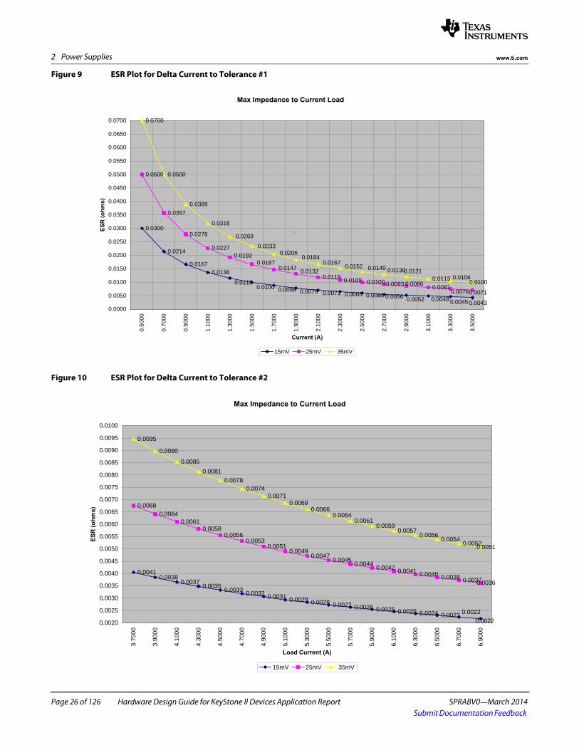
The following three plots show the recommended maximum impedance to current transient for three different tolerances (15 mV, 25 mV, and 35 mV). The first plot covers an allowable current between 500 mA and 3500 mA. The second plot covers 3700 mA to 6900 mA, and the final plot covers 7000 mA to 13000 mA.
The expected maximum current for the KeyStone II device (core) will depend heavily on the use case and design of the application hardware. The recommended components are designed to support up to 17 A (at 86% efficiency) and up to 19 A when using the recommended components and implementing them correctly at 86% efficiency. It does not include current transients that occur during power on (yet these must be considered). Given the recommended topology, only a reduced amount of bulk capacitors is possible, provided they are chosen for there ESR/ESL and voltage rating properly. The majority of all core bulk capacitors must be located in close proximity to the UCD7242 dual FETs.
Capacitance values should not be less than those specified in the applicable table in Section 2.4.4. Final capacitor selection is determined using the provided capacitor selection tool (see spreadsheet and application note).
Some intermediate size ceramic bulk capacitors (i.e., 22 μF and 47 μF as listed under Section 2.4.2) are recommended to cover the response time between the bypass capacitors and the larger bulk capacitors.
SPRABV0—March 2014 Hardware Design Guide for KeyStone II Devices Application Report Page 27 of 126Submit Documentation Feedback
2 Power Supplieswww.ti.com
Figure 11 ESR Plot for Delta Current to Tolerance #3
2.4.1.1 Bulk Capacitor Details and PlacementPlacement of the bulk capacitors is highly dependent on the power supply solution selected. It is important to review the application documents associated with the power supply selected to determine the best placement of the bulk capacitors for your design. Generally, the bulk capacitors are placed in close proximity to the power supply. For the purpose of this document and related devices, a bulk capacitor is defined as any capacitor 22 F, unless otherwise noted.
2.4.2 Selecting Intermediate Value CapacitorsAll intermediate capacitors must be positioned as close to the device as possible, decoupling capacitors taking precedence where placement between the two form factors and values come into question. Intermediate capacitor values are considered to be those between 22 F and 47 F, and they should be low ESR and ceramic, where possible.
2.4.3 Selecting Decoupling CapacitorsAll decoupling or bypass capacitors must be positioned close to the device. In practice, each decoupling capacitor should be placed a maximum distance of 10 mm from the respective pin(s). Where possible, each decoupling capacitor should be tied directly between the respective device pin and ground without the use of traces. Any parasitic inductance limits the effectiveness of the decoupling capacitors; therefore, the physically smaller the capacitors are (0402 or 0201 are recommended), the better the power supply will function.
Page 28 of 126 Hardware Design Guide for KeyStone II Devices Application Report SPRABV0—March 2014Submit Documentation Feedback
2 Power Supplies www.ti.com
Proper capacitance values are also important. All small decoupling or bypass capacitors (560 pF, 0.001 F, 0.01 F, and 0.1 F) must be placed closest to the respective power pins on the target device. Medium bypass capacitors (100 nF or as large as can be obtained in a small package such as an 0402) should be the next closest. TI recommends placing decoupling capacitors immediately next to the BGA vias, using the interior BGA space and at least the corners of the exterior.
The inductance of the via connect can eliminate the effectiveness of the capacitor so proper via connections are important. Trace length from the pad to the via should be no more than 10 mils and the width of the trace should be the same width as the pad. If necessary, placing decoupling capacitors on the back side of the board is acceptable provided the placement and attachment is designed correctly.
2.4.3.1 Decoupling Capacitor Details and PlacementAll decoupling capacitors should be placed in close proximity to the device power pins. For the purpose of this document and related devices, a decoupling or bypass capacitor shall be defined as any capacitor < 1 F, unless otherwise noted.
The table below shows minimum recommended decoupling capacitor values. Each decoupling or bypass capacitor should be directly coupled to the device via. Where direct coupling is impractical, use a trace 10 mil (0.010"/0.254 mm) or shorter, and having the same width as the capacitor pad, is strongly recommended. The table values are minimums; many variables will have an effect on the performance of the power supply system. Re-evaluate the individual power supply design for all variables before implementing the final design.
2.4.4 Example CapacitanceThe following table establishes the bulk and decoupling capacitance requirements for the various device voltage rails. In many cases these rails originate from a common source, which accounts for a reduction in bulk capacitance for many rails. This table does not cover the additional capacitance (decoupling or bulk) required by any other components or the filters outlined in previous sections. All capacitance identified assumes the use of the recommended power supplies (especially for the variable core), and switching frequencies as indicated (see the note section). The recommended values are in addition to those required for proper operation of the recommended power supplies.
The values identified in the following table are per device and assume a typical loading per device IO. In the event multiple devices are used and a voltage rail is common or shared (where applicable), the capacitor requirements must be re-evaluated (on a case-by-case basis) and take into account key concepts including current (load), minimum and maximum current requirements, voltage step, power supply switching frequency, and component ESR. Other constraints also apply.
SPRABV0—March 2014 Hardware Design Guide for KeyStone II Devices Application Report Page 29 of 126Submit Documentation Feedback
2 Power Supplieswww.ti.com
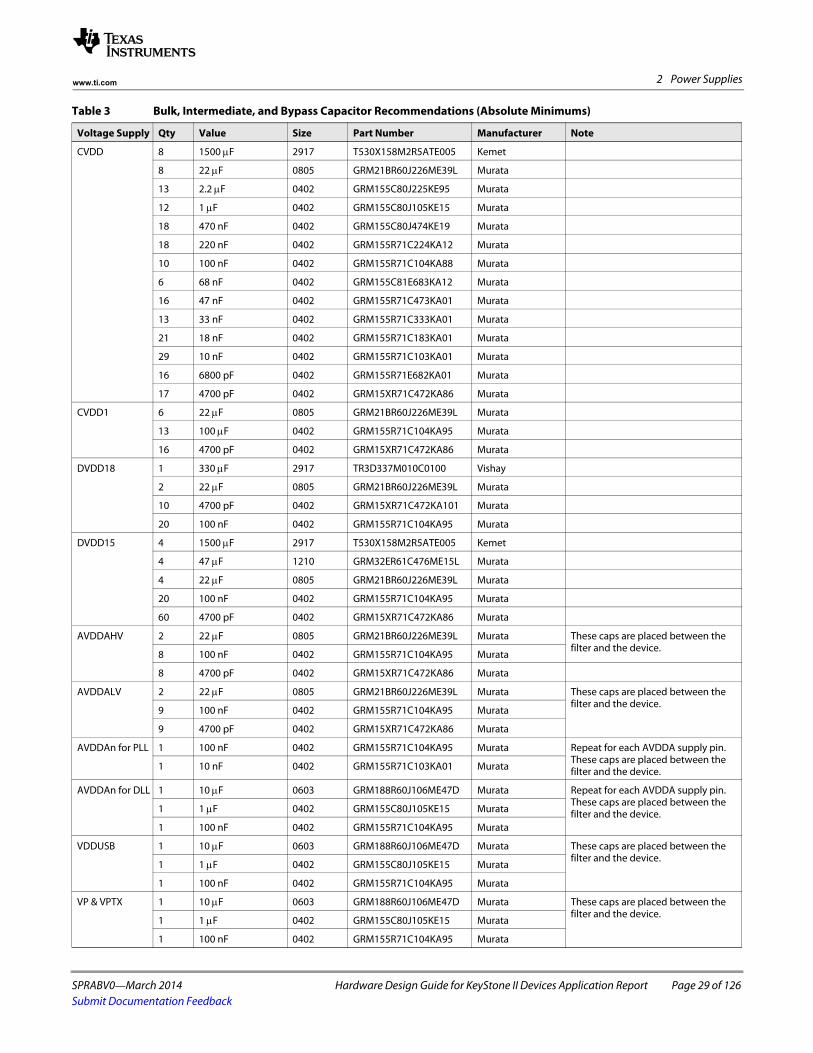
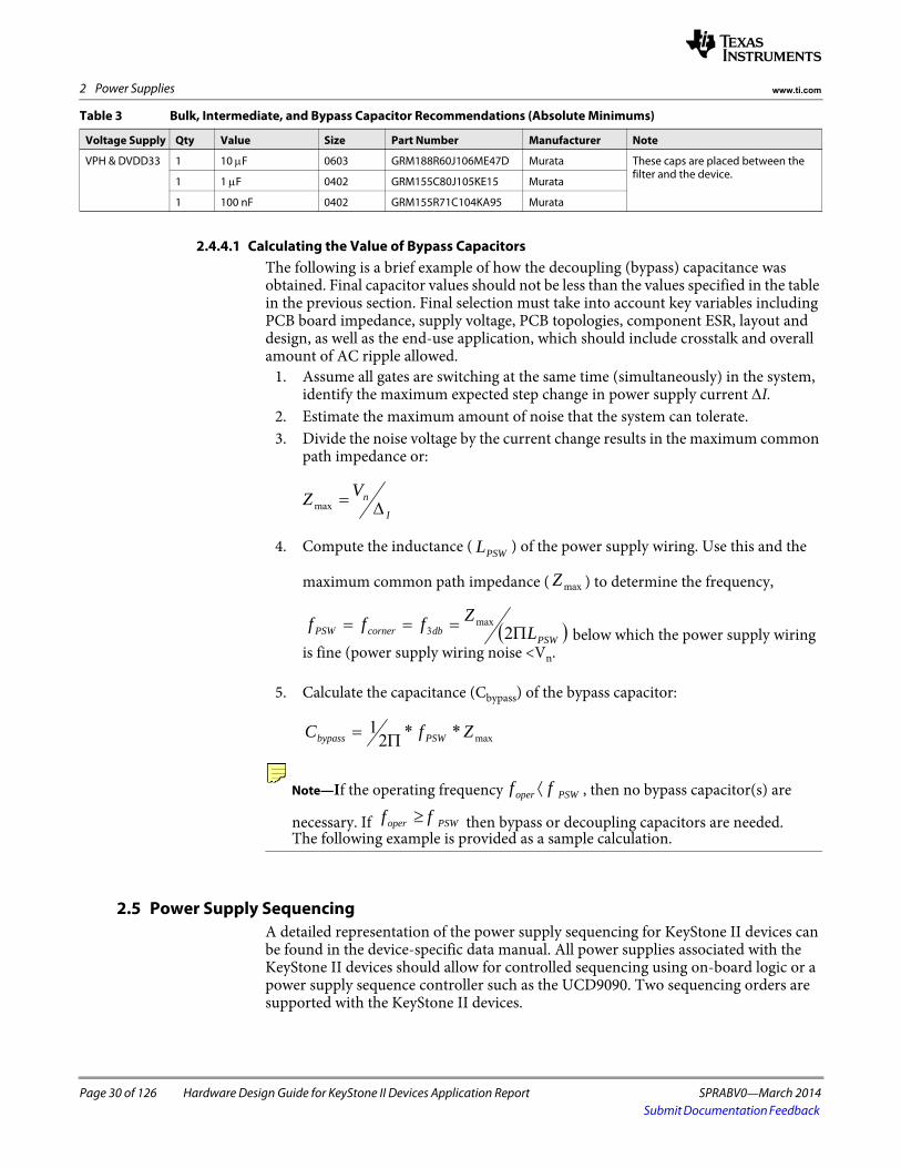
Table 3 Bulk, Intermediate, and Bypass Capacitor Recommendations (Absolute Minimums)
Voltage Supply Qty Value Size Part Number Manufacturer Note
CVDD 8 1500 F 2917 T530X158M2R5ATE005 Kemet
8 22 F 0805 GRM21BR60J226ME39L Murata
13 2.2 F 0402 GRM155C80J225KE95 Murata
12 1 F 0402 GRM155C80J105KE15 Murata
18 470 nF 0402 GRM155C80J474KE19 Murata
18 220 nF 0402 GRM155R71C224KA12 Murata
10 100 nF 0402 GRM155R71C104KA88 Murata
6 68 nF 0402 GRM155C81E683KA12 Murata
16 47 nF 0402 GRM155R71C473KA01 Murata
13 33 nF 0402 GRM155R71C333KA01 Murata
21 18 nF 0402 GRM155R71C183KA01 Murata
29 10 nF 0402 GRM155R71C103KA01 Murata
16 6800 pF 0402 GRM155R71E682KA01 Murata
17 4700 pF 0402 GRM15XR71C472KA86 Murata
CVDD1 6 22 F 0805 GRM21BR60J226ME39L Murata
13 100 F 0402 GRM155R71C104KA95 Murata
16 4700 pF 0402 GRM15XR71C472KA86 Murata
DVDD18 1 330 F 2917 TR3D337M010C0100 Vishay
2 22 F 0805 GRM21BR60J226ME39L Murata
10 4700 pF 0402 GRM15XR71C472KA101 Murata
20 100 nF 0402 GRM155R71C104KA95 Murata
DVDD15 4 1500 F 2917 T530X158M2R5ATE005 Kemet
4 47 F 1210 GRM32ER61C476ME15L Murata
4 22 F 0805 GRM21BR60J226ME39L Murata
20 100 nF 0402 GRM155R71C104KA95 Murata
60 4700 pF 0402 GRM15XR71C472KA86 Murata
AVDDAHV 2 22 F 0805 GRM21BR60J226ME39L Murata These caps are placed between the filter and the device.
8 100 nF 0402 GRM155R71C104KA95 Murata
8 4700 pF 0402 GRM15XR71C472KA86 Murata
AVDDALV 2 22 F 0805 GRM21BR60J226ME39L Murata These caps are placed between the filter and the device.
9 100 nF 0402 GRM155R71C104KA95 Murata
9 4700 pF 0402 GRM15XR71C472KA86 Murata
AVDDAn for PLL 1 100 nF 0402 GRM155R71C104KA95 Murata Repeat for each AVDDA supply pin. These caps are placed between the filter and the device.1 10 nF 0402 GRM155R71C103KA01 Murata
AVDDAn for DLL 1 10 F 0603 GRM188R60J106ME47D Murata Repeat for each AVDDA supply pin. These caps are placed between the filter and the device.1 1 F 0402 GRM155C80J105KE15 Murata
1 100 nF 0402 GRM155R71C104KA95 Murata
VDDUSB 1 10 F 0603 GRM188R60J106ME47D Murata These caps are placed between the filter and the device.
1 1 F 0402 GRM155C80J105KE15 Murata
1 100 nF 0402 GRM155R71C104KA95 Murata
VP & VPTX 1 10 F 0603 GRM188R60J106ME47D Murata These caps are placed between the filter and the device.
Page 30 of 126 Hardware Design Guide for KeyStone II Devices Application Report SPRABV0—March 2014Submit Documentation Feedback
2 Power Supplies www.ti.com
2.4.4.1 Calculating the Value of Bypass CapacitorsThe following is a brief example of how the decoupling (bypass) capacitance was obtained. Final capacitor values should not be less than the values specified in the table in the previous section. Final selection must take into account key variables including PCB board impedance, supply voltage, PCB topologies, component ESR, layout and design, as well as the end-use application, which should include crosstalk and overall amount of AC ripple allowed.
1. Assume all gates are switching at the same time (simultaneously) in the system, identify the maximum expected step change in power supply current I.
2. Estimate the maximum amount of noise that the system can tolerate.3. Divide the noise voltage by the current change results in the maximum common
path impedance or:
4. Compute the inductance ( ) of the power supply wiring. Use this and the
maximum common path impedance ( ) to determine the frequency,
below which the power supply wiringis fine (power supply wiring noise <Vn.
5. Calculate the capacitance (Cbypass) of the bypass capacitor:
Note—If the operating frequency , then no bypass capacitor(s) are
necessary. If then bypass or decoupling capacitors are needed. The following example is provided as a sample calculation.
2.5 Power Supply SequencingA detailed representation of the power supply sequencing for KeyStone II devices can be found in the device-specific data manual. All power supplies associated with the KeyStone II devices should allow for controlled sequencing using on-board logic or a power supply sequence controller such as the UCD9090. Two sequencing orders are supported with the KeyStone II devices.
VPH & DVDD33 1 10 F 0603 GRM188R60J106ME47D Murata These caps are placed between the filter and the device.
1 1 F 0402 GRM155C80J105KE15 Murata
1 100 nF 0402 GRM155R71C104KA95 Murata
Table 3 Bulk, Intermediate, and Bypass Capacitor Recommendations (Absolute Minimums)
Voltage Supply Qty Value Size Part Number Manufacturer Note
A power supply should reach a valid voltage level and declare the supply output in a power good state before enabling the next supply in the sequence.
2.6 Power Supply Block DiagramNow that the power supply components have been selected, create a power supply block diagram similar to the one found in the EVM schematic for the KeyStone II devices. This block diagram should include all of the power supplies in the design, the output voltage associated with each, the current limit, and the signal used to enable the supply. A second diagram showing the sequencing of the supplies should also be generated. These documents will be requested by Texas Instruments if support is needed. They should be added to the design folder and it is good practice to include them in the schematics for reference.
Page 32 of 126 Hardware Design Guide for KeyStone II Devices Application Report SPRABV0—March 2014Submit Documentation Feedback
3 Clocking www.ti.com
3 ClockingThe next requirement for the KeyStone II design is proper clocking. KeyStone II devices include a number of internal PLLs that are used to generate the clocks within the part. These include PLLs for generating system clocks and PLLs for the high speed SerDes interfaces. All clocks must meet the specified stability and jitter requirements from the device data manual for successful operation of the design. This section describes the clocks found in KeyStone II devices and the requirements for these clocks. Detailed clock input requirements are found in the device-specific data manual. Not all of the clocks described in this section will appear on every KeyStone II device. See the device-specific data manual to determine which clocks are present in your KeyStone II device.
3.1 System PLL Clock InputsThe system PLL clock inputs for KeyStone II devices are shown in Table 4.
All system PLL clock inputs are differential and must be driven by one of the specified differential driver types. All the differential clock inputs specified in Table 4 are implemented with Texas Instruments low jitter clock buffers (LJCBs). These input buffers include a 100- parallel termination (P to N) and common-mode biasing. Because the common-mode biasing is included, the clock source must be AC coupled. Low-voltage differential swing LVDS and LVPECL clock sources are compatible with the LJCBs. A separate, properly terminated clock driver must be provided for each clock input. The proper termination for the clock driver selected must be included. Not all clock drivers are terminated in the same manner. See the data manual for the proper termination of the clock driver you have selected. For additional information on AC termination schemes, see the AC-Coupling Between Differential LVPECL, LVDS, and CML Application Report (SCAA059). Note that the LJCB clock input is assumed to be a CML input in this document.
Table 4 KeyStone II System PLL Clock Inputs
ClockFrequency Range (MHz)
Drivers Supported Description
CORECLKpCORECLKn
40-312.5 LVDS, LVPECL(AC Coupled)
Used to clock the Main PLL
ALTCORECLKpALTCORECLKn
40-312.5 LVDS, LVPECL(AC Coupled)
Used to clock the Main PLL if CORECLKSEL = 1
ARMCLKpARMCLKn
40-312.5 LVDS, LVPECL(AC Coupled)
Used to clock the ARM CorePac PLL
DDRCLKpDDRCLKn
40-312.5 LVDS, LVPECL(AC Coupled)
Used to clock the DDR PLL
DDR3ACLKpDDR3ACLKn
40-312.5 LVDS, LVPECL(AC Coupled)
Used to clock the DDR A PLL
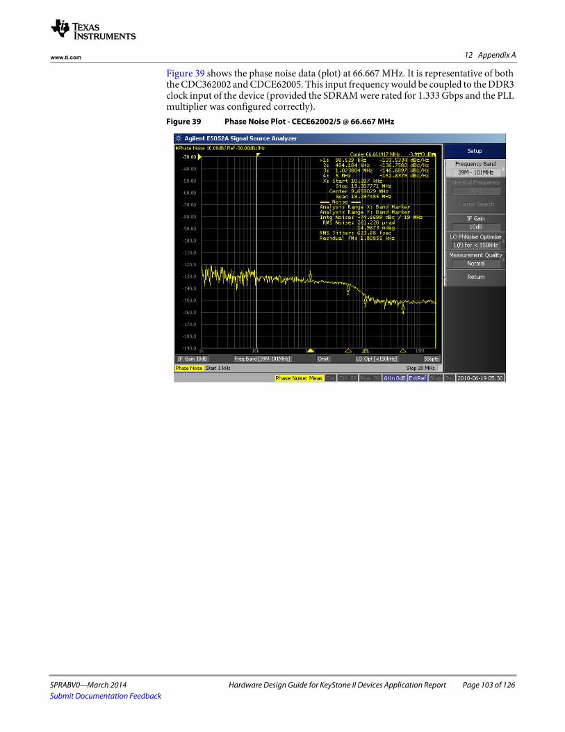
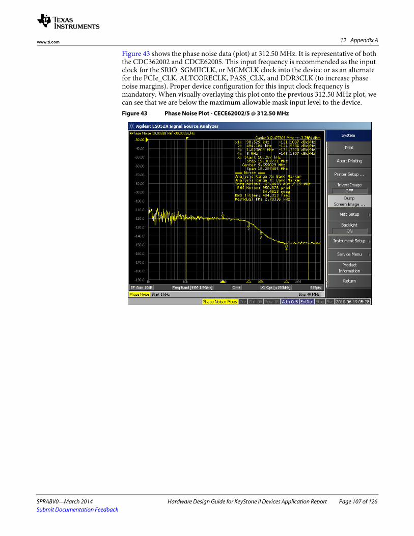
DDR3BCLKpDDR3BCLKn
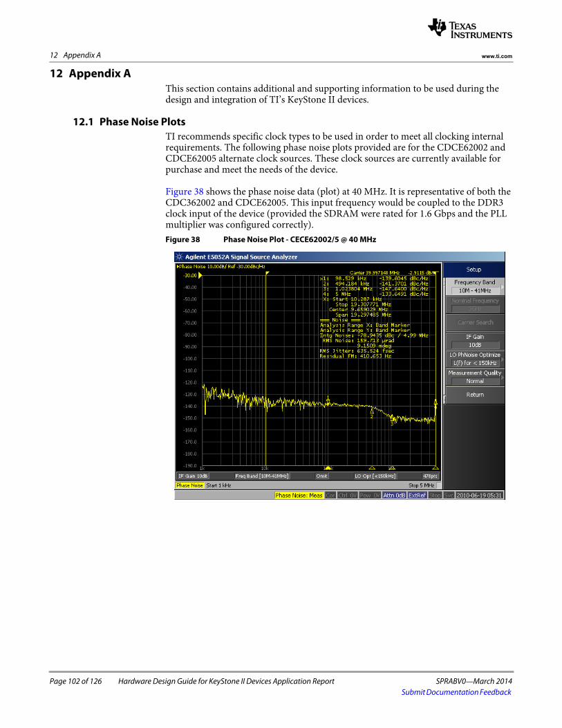
40-312.5 LVDS, LVPECL(AC Coupled)
Used to clock the DDR B PLL
PASSCLKpPASSCLKn
40-312.5 LVDS, LVPECL(AC Coupled)
Used to clock the packet accelerator subsystem PLL if PASSCLKSEL = 1
NETCPCLKpNETCPCLKn
40-312.5 LVDS, LVPECL(AC Coupled)
Used to clock the Network Coprocessor PLL if NETCPCLKSEL = 1
SPRABV0—March 2014 Hardware Design Guide for KeyStone II Devices Application Report Page 33 of 126Submit Documentation Feedback
3 Clockingwww.ti.com
These clock inputs are used by system PLLs to generate the internal clocks needed to operate the device. These PLLs are compatible with a wide range of clock input frequencies, which can be multiplied to the valid operating frequencies of the device. Detailed information on programming the PLLs can be found in the Phase-Locked Loop (PLL) for KeyStone Devices Users Guide.
The main PLL is driven in one of two manners, depending on the device. • It is driven by CORECLKP/N if a dedicated main PLL clock input is present on
the device.• It is driven by either the ALTCORECLKP/N or the SYSCLKP/N depending on
the state of the CORECLKSEL configuration input.
Some KeyStone II devices allow one of two clock inputs to be used as a source for the main PLL. If ALTCORECLKP/N is selected, it acts as a dedicated clock input for the main PLL. SYSCLKP/N is also used as a clock source for the AIF interface and is considered a SerDes PLL clock source. If SYSCLKP/N is selected it will be the clock source for both the main PLL and the AIF interface.
3.1.1 System Reference Clock RequirementsTable 5 shows the specific input clocking requirements for the KeyStone II device, including maximum input jitter, rise and fall times, and duty cycle. When discrepancies occur between the data manual and this application note, always use the latest device-specific data manual.
Figure 12 shows the rise and fall time requirements for the KeyStone II system reference clocks. System reference clocks are always differential and the rise and fall times are measured on the V(pk-pk) of the differential input. The minimum V(pk-pk) of these clocks is 250 mV and the rise and fall times are measured on 10% to 90% of the
Table 5 KeyStone II System PLL Clocking Requirements — Jitter, Duty Cycle, tr / tf
2.0% of CORECLK input period (pk-pk) 50 – 350 ps1 45 / 55 ± 100 PPM
ALTCORECLKpALTCORECLKn
2.0% of ALTCORECLK input period (pk-pk) 50 – 350 ps1 45 / 55 ± 100 PPM
ARMCLKpARMCLKn
2.0% of ALTCORECLK input period (pk-pk) 50 – 350 ps1 45 / 55 ± 100 PPM
DDRCLKpDDRCLKn
2.0% of DDRCLK input period (pk-pk) 50 – 350 ps1 45 / 55 ± 100 PPM
DDR3ACLKpDDRCLKn
2.0% of DDRCLK input period (pk-pk) 50 – 350 ps1 45 / 55 ± 100 PPM
DDR3BCLKpDDRCLKn
2.0% of DDRCLK input period (pk-pk) 50 – 350 ps1 45 / 55 ± 100 PPM
PASSCLKpPASSCLKn
2.0% of PASSCLK input period (pk-pk) 50 – 350 ps1 45 / 55 ± 100 PPM
NETCPCLKpNETCPCLKn
2.0% of PASSCLK input period (pk-pk) 50 – 350 ps1 45 / 55 ± 100 PPM
End of Table 51. Swing is rated for a 200 mV (pk-pk) at zero crossing, which is 10% – 90% of the minimum 250 mV (pk-pk) of the input clock signal. trise and tfall must occur within the
prescribed 50-ps to 350-ps time frame. This is shown below.
Page 34 of 126 Hardware Design Guide for KeyStone II Devices Application Report SPRABV0—March 2014Submit Documentation Feedback
3 Clocking www.ti.com
minimum V(pk-pk) or 200 mV. Regardless of the actual V(pk-pk) level, the rise and fall time spec must be met only for the 200 mV around the zero crossing. When discrepancies occur between the data manual and this application note, always use the latest device-specific data manual. Figure 12 System Clock Rise Time
3.2 SerDes PLL Reference Clock InputsKeyStone II devices contain several high-performance serial interfaces commonly known as SerDes interfaces. The Serializer/Deserializer (SerDes) PLL reference clock inputs for KeyStone II devices are shown in Table 6.
Not all clock inputs are present on all KeyStone devices. Check the device-specific data manual for a complete list of clock inputs. All clock inputs are differential and must be driven by one of the specified differential driver types.
200mV transition voltage range0
peak-to-peak differential inputvoltage (250mV to 2V)
TR = 50ps min to 350ps max for 200mV transition voltage range.
Table 6 KeyStone II SerDes PLL Reference Clock Inputs
Clock Valid Input Frequencies (MHZ)Input Buffer Type Drivers Supported Description
SPRABV0—March 2014 Hardware Design Guide for KeyStone II Devices Application Report Page 35 of 126Submit Documentation Feedback
3 Clockingwww.ti.com
Some of the SerDes reference differential clock inputs are implemented with Texas Instruments low jitter clock buffers (LJCBs). These input buffers include a 100- parallel termination (P to N) and common-mode biasing. Because the common mode biasing is included, the clock source must be AC coupled. Low-voltage differential swing LVDS and LVPECL clock sources are compatible with the LJCBs. Termination on the driver side of the AC coupling capacitors may still be needed. See the data manual for the driver selected for the proper termination.
Many of the SerDes reference clocks for the KeyStone II devices are connected directly to the clock input circuit of the SerDes IP. The internal clock input circuit for these references include the AC coupling capacitors as well as the 100- parallel termination (P to N) and common-mode biasing. Termination for the driver may still be needed. This termination should be place between the driver and the clock reference input pins. See the data manual for the driver selected for the proper termination.
The USB clock reference input buffer is not the same on all KeyStone II devices. On some devices the LJCB buffer is implemented and the clock can be connected as described above. In some devices an LJCB buffer is not present for the USB clock reference. External AC coupling capacitors are needed to connect the USB reference clock to the KeyStone II device. If LJCB is not used, the peak-to-peak differential input voltage range for the USB reference clock is limited to 850 mV(pk-pk). To meet this requirement, some drivers may require additional termination to limit the voltage swing of the clock input. For example, the peak-to-peak differential voltage output of an LVPECL driver can be as high as 1400 mV(pk-pk), which exceeds the input voltage limits. A series resistor before the AC coupling capacitor can be used to attenuate the LVPECL output to satisfy the input voltage requirement.
Clock drivers may source only one clock input, so a separate clock driver must be provided for each clock input. In addition, the proper termination for the clock driver selected must be included. For additional information on AC termination schemes, see the AC-Coupling Between Differential LVPECL, LVDS, and CML Application Report (SCAA059). Note that the LJCB clock input is assumed to be a CML input in this document.
Spread spectrum clocks are commonly used with PCI express and a may be present on a PCI express bus connector. The PCIECLKP/N input is compatible with PCI express-compliant spread-spectrum clocking. Note that a common clock for a PCI express root complex and endpoint are not required unless a spread-spectrum clock is used. If a spread-spectrum clock is used by one device at the far end of a PCI express link, the same clock must be used as a reference by the KeyStone II device.
These clock inputs are used by PLLs in the reference SerDes interface. These interfaces require high-quality clocks with low phase noise and are specified only to operate with specific reference clock input frequencies. Detailed information on programming the PLL associated with a reference clock input can be found in the user guide for that SerDes interface.
3.2.1 SerDes Reference Clock Rise and Fall RequirementsThe rise and fall time requirements for a KeyStone II SerDes reference clock is dependent on the input buffer. The input buffer type for each SerDes reference clock are shown in Table 6. There are three specific input buffer types used for the SerDes Reference clock. These are specified in the data manual for your KeyStone II device. The rise and fall times for SerDes reference clocks that use the LJCB input buffer are
Page 36 of 126 Hardware Design Guide for KeyStone II Devices Application Report SPRABV0—March 2014Submit Documentation Feedback
3 Clocking www.ti.com
shown in Figure 12 within the System Reference Clocks section. The minimum V(pk-pk) of these clocks is 250 mV and the rise and fall times are measured on 10% to 90% of the minimum V(pk-pk), or 200 mV. Regardless of the actual V(pk-pk) level, the rise and fall time spec must be met only for the 200 mV around the zero crossing. The rise and fall time for SerDes reference clocks using the SerDes/CML input buffer are shown in Figure 13. Note that the rise and fall time must be met for 10% to 90% of the peak-to-peak differential voltage level. Figure 13 SerDes/CML Clock Rise Time
The exception to this is the USB reference clock. In some devices, this clock uses the LJCB buffer. In other devices, it must meet the peak-to-peak voltage limits and the rise and fall time limits shown in Figure 14. The rise time can be no less then 75 ps and no more then 500 ps for the 300 mV(pk-pk) around the center of the differential peak-to-peak voltage.
Figure 14 USB Clock Rise Time
3.2.2 SerDes Reference Clock Jitter RequirementsThe SerDes architecture allows for reliable data transmission without a need for common synchronized clocks. However, the architecture does require high-quality clock sources that have very little phase noise. Phase noise is also commonly referred to as clock jitter.
Note that PCIe can be operated with a common clock, which allows for the use of spread-spectrum clock sources that have higher levels of bounded phase noise. HyperLink is also defined as an interface requiring a common clock because it is expected to be a very short-reach interface between DSPs located on the same board.
0peak-to-peak differential input
voltage (400mV to 1100mV)
10% to 90% of peak-to-peak voltage.
max TR = 0.2 * TC from 10% to 90% of the peak-to-peak differential voltage.
TC reference clock period
max TF = 0.2 * TC from 10% to 90% of the peak-to-peak differential voltage.
0peak-to-peak differential input
voltage (300mV to 850mV)
TR = 75ps min to 500ps max for 300mV transition voltage range.
TF = 75ps min to 500ps max for 300mV transition voltage range.
SPRABV0—March 2014 Hardware Design Guide for KeyStone II Devices Application Report Page 37 of 126Submit Documentation Feedback
3 Clockingwww.ti.com
3.2.2.1 Random JitterPhase noise amplitude is not the only concern. The frequency content of this phase noise is also significant. Therefore, masks are provided as a means of indicating an acceptable phase noise tolerance. Each SerDes interface has a slightly different jitter requirement. SerDes data rate, input clock rate, and required bit-error rate affect the phase noise tolerance.
Table 7 defines the input jitter requirements for each of the SerDes reference clocks. Note that the RMS is calculated from 100 kHz to 20 MHz. The input jitter value includes a limit expressed as a initial jitter value with an additional value that should be subtracted.
3.2.2.2 Deterministic JitterReference clock sources may also contain deterministic jitter in the form of spurs that must also be accounted for. The effects of spurs vary depending upon whether they are correlated or uncorrelated. An exact determination of the effects of the spurs would be very complicated. (There are published papers concerning the complexities of combining the noise power of spurs.) A simplified formula is shown below:
The limit of 0.1 ps is a level chosen to provide a reasonable margin without complex analysis. This equation has sufficient margin to be used for all interface types and baud rates.
Table 7 SerDes Reference Clock Jitter Requirement
Clock Input Jitter Note
SYSCLK 4 ps RMS - 178 fs 53.8 ps pk-pk total jitter when AIF is used
SRIOSGMIICLK 1.88 ps RMS - 178 fs
1.88 ps RMS - 178 fs
3.97 ps RMS - 178 fs
23.94 ps pk-pk total jitter when both SRIO and SGMII are used
23.94 ps pk-pk total jitter when only SRIO is used
53.35 ps pk-pk total jitter when only SGMII is used
SGMIICLK 3.97 ps RMS - 178 fs 53.35 ps pk-pk total jitter when only SGMII is used
Page 38 of 126 Hardware Design Guide for KeyStone II Devices Application Report SPRABV0—March 2014Submit Documentation Feedback
3 Clocking www.ti.com
3.3 Unused Clock InputsAny unused LJCB or LVDS differential clock inputs should be connected to the appropriate rails to establish a valid logic level. Unused clock inputs connected to the SerDes/CML in the KeyStone II device should be left unconnected.
The recommended connections are shown in Figure 15. The added 1-k resistor is included to reduce power consumption. The positive terminal should be connected to the CVDD power rail. Figure 15 Unused LJCB Clock Input Connection
The recommended connections for unused LVDS inputs are shown in Figure 16. The added 1-k resistors are included to reduce power consumption. The positive terminal should be connected to the DVDD18 power rail. Figure 16 Unused LVDS Clock Input Connection
SPRABV0—March 2014 Hardware Design Guide for KeyStone II Devices Application Report Page 39 of 126Submit Documentation Feedback
3 Clockingwww.ti.com
Table 8 shows the specific rails to which each unused clock input should be connected (in accordance with Figure 15).
3.3.1 BER and JitterExcessive jitter can cause data errors, for this reason (and usually in high-performance data transmission protocols) a BER (bit error rate) is usually specified to minimize the risk of an error occurring. Jitter is the sum of both random and deterministic sources. In an ideal design, all jitter is identified as undesirable.
Connect P to supply railConnect N to ground through 1-k resistor
ALTCORECLKPALTCORECLKN
LJCB CVDDGND
Connect P to supply railConnect N to ground through 1-kresistor
ARMCLKPARMCLKN
LJCB CVDDGND
Connect P to supply railConnect N to ground through 1K resistor
DDRCLKPDDRCLKN
LJCB CVDDGND
Connect P to supply railConnect N to ground through 1-kresistor
DDR3ACLKPDDR3ACLKN
LJCB CVDDGND
Connect P to supply railConnect N to ground through 1-kresistor
DDR3BCLKPDDR3BCLKN
LJCB CVDDGND
Connect P to supply railConnect N to ground through 1-kresistor
PASSCLKPPASSCLKN
LJCB CVDDGND
Connect P to supply railConnect N to ground through 1-kresistor
NETCPCLKPNETCPCLKN
LJCB CVDDGND
Connect P to supply railConnect N to ground through 1-kresistor
SYSCLKPSYSCLKN
LJCB CVDDGND
Connect P to supply railConnect N to ground through 1-kresistor
SRIOSGMIICLKPSRIOSGMIICLKN
LJCB CVDDGND
Connect P to supply railConnect N to ground through 1-kresistor
SGMIICLKPSGMIICLKN
LJCB CVDDGND
Connect P to supply railConnect N to ground through 1-kresistor
PCIECLKPPCIECLKN
SerDes/CML N/A Leave unconnected
HYP0CLKPHYP0CLKN
SerDes/CML N/A Leave unconnected
HYP1CLKPHYP1CLKN
SerDes/CML N/A Leave unconnected
XFICLKPXFICLKN
SerDes/CML N/A Leave unconnected
USBCLKPUSBCLKN
SerDes/CML 2 N/A Leave unconnected
USBCLKPUSBCLKN
LJCB 3 CVDDGND
Connect P to supply railConnect N to ground through 1-kresistor
RP1CLKPRP1CLKN
LVDS DVDD18 GND
Connect P to supply rail through 1-kresistorConnect N to ground through 1-kresistor
RP1FBPRP1FBN
LVDS DVDD18 GND
Connect P to supply rail through 1-kresistorConnect N to ground through 1-kresistor
End of Table 81. The power rails must be identical to those directly supporting the intended device2. For KeyStone II devices that use SerDes/CML for the USBCLK input buffer3. For KeyStone II devices that use LJCB for the USBCLK input buffer
Page 40 of 126 Hardware Design Guide for KeyStone II Devices Application Report SPRABV0—March 2014Submit Documentation Feedback
3 Clocking www.ti.com
Random jitter can be defined as the sum of all noise sources including components used to construct and implement the data path between source and target. Random jitter is considered unbounded and will continue to increase over time. Random jitter can theoretically reach infinity. Some sources of random or unbounded jitter include:
• Shot noise [electron and hole noise in a semiconductor - increasing due to bias current and measurement bandwidth].
• Thermal noise [associated with electron flow in conductors, variations due to temperature, bandwidth, and noise resistance].
• Flicker or pink noise [spectral noise related to 1/ƒ].
Deterministic jitter, unlike random Jitter, is the total jitter induced by the characteristics of the data path between source and target. Deterministic jitter, also called bounded jitter, obtains its minimum or maximum phase deviation within the respective time interval. Sources of deterministic jitter include (most prominently):
• Electromagnetic Interference radiation (EMI) from power supplies, AC power lines, and RF-signal sources.
• Crosstalk (occurs when incremental inductance from one signal line (conductor) converts an induced magnetic field from an adjacent signal line into induced current resulting in either an increase or decrease in voltage.
• Inter-Symbol Interference (ISI) increases in deterministic jitter of this nature can be caused by either simultaneous switching (inducing current spikes on power or ground planes possibly causing a voltage threshold level shift) or a reflection in the signal or transmission line. Reflections result in energy flowing back through the conductor that sum with the original signal causing an amplitude variation on each conductor within a differential pair resulting in a specific time variation of the crossover (crossing) points.
Given a specific BER and an equivalent RMS jitter value, a peak-to-peak (pk-pk) jitter value can be determined (assuming a truly Gaussian or random distribution). The following calculation can be used to approximate total jitter:
The Random pk-pk jitter is a function of the BER and RMS jitter as denoted in the following equation:
SPRABV0—March 2014 Hardware Design Guide for KeyStone II Devices Application Report Page 41 of 126Submit Documentation Feedback
3 Clockingwww.ti.com
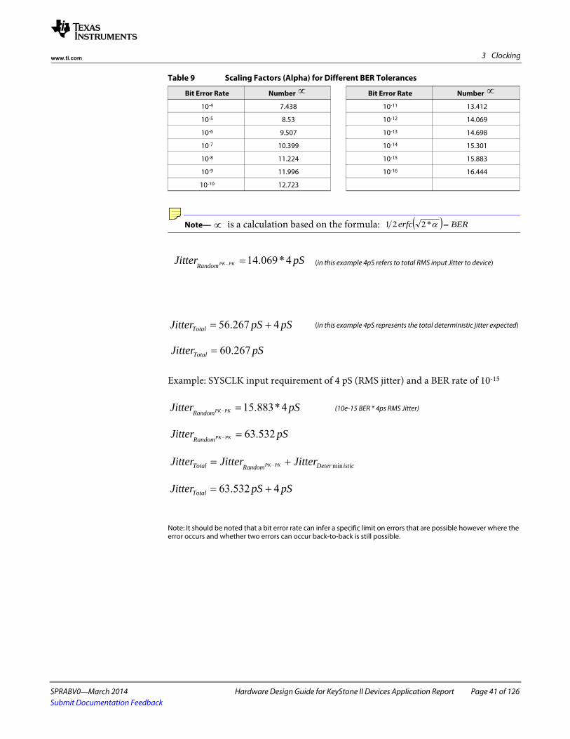
Note— is a calculation based on the formula:
Example: SYSCLK input requirement of 4 pS (RMS jitter) and a BER rate of 10-15
Note: It should be noted that a bit error rate can infer a specific limit on errors that are possible however where the error occurs and whether two errors can occur back-to-back is still possible.
Table 9 Scaling Factors (Alpha) for Different BER Tolerances
Bit Error Rate Number Bit Error Rate Number
10-4 7.438 10-11 13.412
10-5 8.53 10-12 14.069
10-6 9.507 10-13 14.698
10-7 10.399 10-14 15.301
10-8 11.224 10-15 15.883
10-9 11.996 10-16 16.444
10-10 12.723
(in this example 4pS refers to total RMS input Jitter to device)
(in this example 4pS represents the total deterministic jitter expected)
Page 42 of 126 Hardware Design Guide for KeyStone II Devices Application Report SPRABV0—March 2014Submit Documentation Feedback
3 Clocking www.ti.com
3.4 Single-ended Clock SourcesUnlike some previous Texas Instruments DSPs, KeyStone II devices do not allow single-ended clock input sources. Differential clock sources provide better noise immunity and signal integrity, and are required by KeyStone II devices.
3.5 Clocking and Clock Trees (Fan out Clock Sources) For systems with multiple high-performance processor devices, a single clock source should not be used to drive multiple clock inputs. Excessive loading, reflections, and noise will adversely impact performance. Clock generators and clock distribution components can be used to drive a common clock source to multiple clock inputs on the KeyStone II device.
Texas Instruments has developed a specific line of clock sources to meet the challenging requirements of today’s high performance devices. In most applications the use of these specific clock sources eliminates the need for external buffers, level translators, external jitter cleaners, or multiple oscillators.
A few of the recommended parts include:• CDCM6208 - Single PLL, 8 Differential Output Clock Tree with 4 Fractional
Dividers• CDCE62005 - Single PLL, 5 Differential Output Clock Tree with Jitter Cleaner• CDCE62002 - Single PLL, 2 Differential Output Clock Tree with Jitter Cleaner• CDCE62005 - Five Output Low Jitter Clock Tree with Jitter Cleaner
Note—These parts are specifically designed for the KeyStone II devices. To minimize cost and maximize performance, all parts accept a differential, single-ended, or crystal input clock source.
See the device-specific data manuals for clock tree input requirements and functionality.
SPRABV0—March 2014 Hardware Design Guide for KeyStone II Devices Application Report Page 43 of 126Submit Documentation Feedback
3 Clockingwww.ti.com
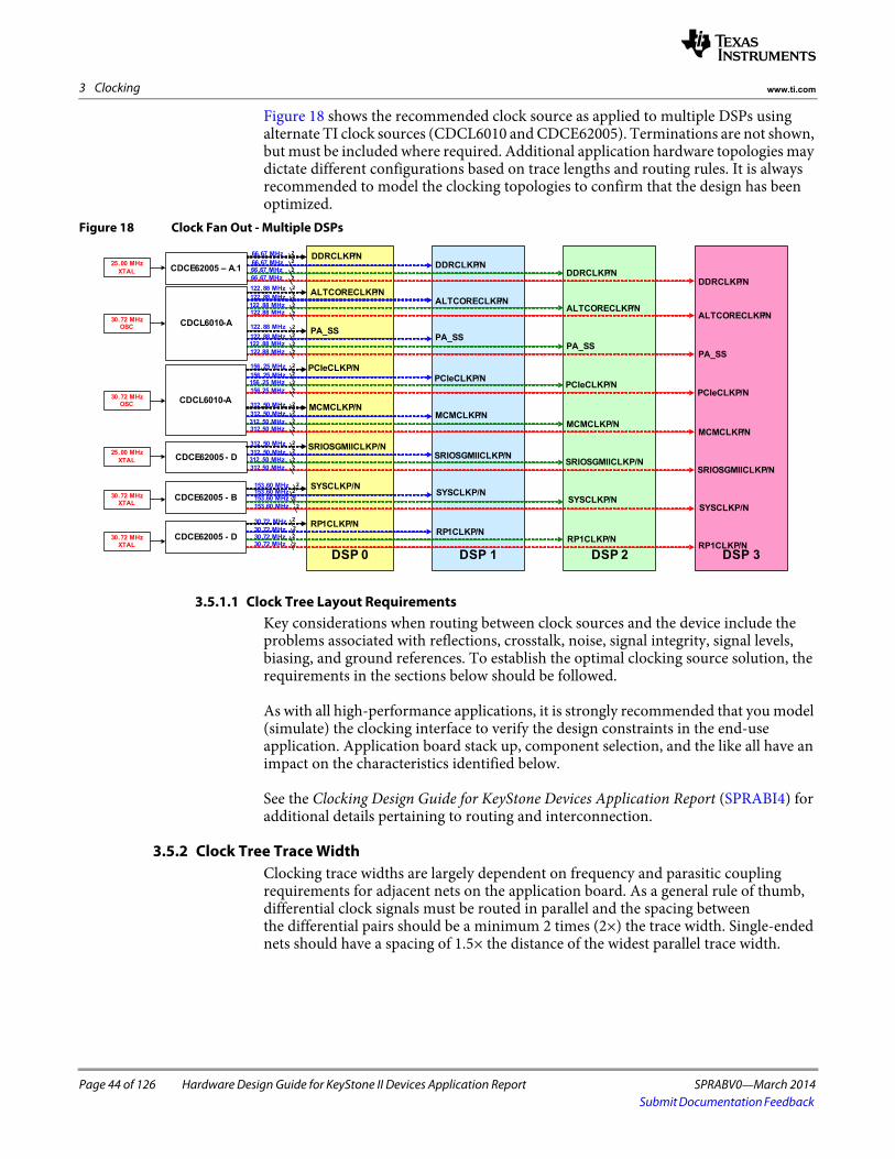
3.5.1 Clock Tree Fanout SolutionThe following section provides examples for routing between a CDCM6208 to one and multiple KeyStone II devices. A similar topology should be used regardless of the end-use application hardware. Figure 17 shows an example of a 6208 used to provide all the clocks needed for a KeyStone II device.Figure 17 Clock Fan Out - for Single Device
The CDCM6208 incorporates fractional dividers. When assigning fractional divider outputs from the CDCM6208, it will be necessary to verify that the input jitter and performance meet or exceed the requirements for the respective device input (select the correct clock outputs for the proper clock inputs).
Page 44 of 126 Hardware Design Guide for KeyStone II Devices Application Report SPRABV0—March 2014Submit Documentation Feedback
3 Clocking www.ti.com
Figure 18 shows the recommended clock source as applied to multiple DSPs using alternate TI clock sources (CDCL6010 and CDCE62005). Terminations are not shown, but must be included where required. Additional application hardware topologies may dictate different configurations based on trace lengths and routing rules. It is always recommended to model the clocking topologies to confirm that the design has been optimized.
Figure 18 Clock Fan Out - Multiple DSPs
3.5.1.1 Clock Tree Layout RequirementsKey considerations when routing between clock sources and the device include the problems associated with reflections, crosstalk, noise, signal integrity, signal levels, biasing, and ground references. To establish the optimal clocking source solution, the requirements in the sections below should be followed.
As with all high-performance applications, it is strongly recommended that you model (simulate) the clocking interface to verify the design constraints in the end-use application. Application board stack up, component selection, and the like all have an impact on the characteristics identified below.
See the Clocking Design Guide for KeyStone Devices Application Report (SPRABI4) for additional details pertaining to routing and interconnection.
3.5.2 Clock Tree Trace WidthClocking trace widths are largely dependent on frequency and parasitic coupling requirements for adjacent nets on the application board. As a general rule of thumb, differential clock signals must be routed in parallel and the spacing between the differential pairs should be a minimum 2 times (2×) the trace width. Single-ended nets should have a spacing of 1.5× the distance of the widest parallel trace width.
SPRABV0—March 2014 Hardware Design Guide for KeyStone II Devices Application Report Page 45 of 126Submit Documentation Feedback
3 Clockingwww.ti.com
3.5.3 Clock Tree SpacingGiven the variation in designs, the minimum spacing between any adjacent signals should be a minimum of 1× the width. A spacing of 1× is typically suitable for control signals (or static signals) and not data or clock nets. Single-ended or differential nets should be spaced from other nets a minimum of 1.5× and 2× respectively. A detailed cross-talk and coupling analysis (signal integrity) should be performed before any design is released to production. An additional rule of thumb would be to maintain trace spacing three times the dielectric height (reduces ground bounce and crosstalk).
3.5.4 Clock Transmission Lines - Microstrip versus StriplineSee Section 10.6 for additional detailed information regarding microstrip and stripline features and selection criteria.
3.5.5 Clock Component Selection & PlacementA proper clock source is critical to ensure the KeyStone II device maintains its intended functionality. TI strongly recommends the use of the clock sources developed to complement the device (see Section 3.5). These clock sources have been optimized for performance, jitter, and form-factor. The recommended clock source (CDCM6208) has been designed to accept either a low frequency crystal, LVPECL, LVDS, HCSL, or LVCMOS input and is capable of sourcing either a LVPECL, LVDS, HCSL, or LVCMOS clock to the KeyStone II device and peripheral logic.
All clock sources should be placed as close to the targeted device(s) as possible. Excessive trace length induces many problems that are costly to correct in the end product and usually require a respin of the application hardware.
Alternative clock sources have been identified and include the CDCE62002 and CDCE62005. These alternative clock sources will provide functionally identical resources when implemented correctly. Additional information regarding the CDCE62002/5 is available in ‘‘Appendix A’’ of this document.
3.5.6 Clock Termination Type and LocationAll input clocks are presumed to be of the differential type and require proper terminations or coupling. Each differential pair must be AC-Coupled using a 0.1-μF ceramic capacitor (0402 size or smaller recommended). In some cases, depending on topology, a 1-μF capacitor can be used. All AC-coupling capacitors should be located at the destination end as close to the device as possible.
Figure 19 shows the intended connection between the clock source and DSP. Figure 19 Clock Termination Location
Page 46 of 126 Hardware Design Guide for KeyStone II Devices Application Report SPRABV0—March 2014Submit Documentation Feedback
3 Clocking www.ti.com
3.6 Clock SequencingTable 10 shows the requirements for input clocks to the KeyStone II device. Time frames indicated are minimum. Maximum timeframes are defined in the data manual and shall not be violated. (See the device-specific data manual for specific timing requirements.)
Note—All clock drivers must be in a high-impedance state until CVDD (at a minimum) is at a valid level. After CVDD is at a valid level, all clock inputs must either be active or in a static state.
Table 10 Clock Sequencing (Part 1 of 2)
Clock Condition Sequencing
DDRCLK None Must be present 16 s before POR transitions high.
DDRCLK3A None Must be present 16 s before POR transitions high.
DDRCLK3B None Must be present 16 s before POR transitions high if used in the design.
SYSCLK CORECLKSEL = 0 SYSCLK used to clock the core PLL. It must be present 16 s before POR transitions high.
CORECLKSEL = 1 SYSCLK only used for AIF. Clock most be present before the reset to the AIF is removed.
CORECLK None CORECLK used to clock the core PLL. It must be present 16 s before POR transitions high.
ARMCLK None ARMCLK used to clock the ARM PLL. It must be present 16 s before POR transitions high.
ALTCORECLK CORECLKSEL = 0 ALTCORECLK is not used and should be terminated as shown in Table 8
CORECLKSEL = 1 ALTCORECLK is used to clock the core PLL. It must be present 16 s before POR transitions high.
PASSCLK PASSCLKSEL = 0 PASSCLK is not used and should be terminated as shown in Table 8
PASSCLKSEL = 1 PASSCLK is used as a source for the PA_SS PLL. It must be present before the PA_SS PLL is removed from reset and programmed.
NETCPCLK NETCPCLKSEL = 0 NETCPCLK is not used and should be terminated as shown in Table 8
NETCPCLKSEL = 1 NETCPCLK is used as a source for the PA_SS PLL. It must be present before the PA_SS PLL is removed from reset and programmed.
SRIOSGMIICLK An SGMII port will be used SRIOSGMIICLK must be present 16 s before POR transitions high
SGMII will not be used. SRIO will be used as a boot device
SRIOSGMIICLK must be present 16 s before POR transitions high.
SGMII will not be used. SRIO will be used after boot
SRIOSGMIICLK is used as a source to the SRIO SerDes PLL. It must be present before the SRIO is removed from reset and programmed.
SGMII will not be used. SRIO will not be used.
SRIOSGMIICLK is not used and should be terminated as shown in Table 8
SGMIICLK An SGMII port will be used SRIOSGMIICLK must be present 16 s before POR transitions high
PCIECLK PCIE will be used as a boot device.
PCIECLK must be present 16 s before POR transitions high.
PCIE will be used after boot. PCIECLK is used as a source to the PCIE SerDes PLL. It must be present before the PCIE is removed from reset and programmed.
PCIE will not be used. PCIECLK is not used and should be terminated as shown in Table 8
HYPLKCLK HyperLink will be used as a boot device.
HYPLKCLK must be present 16 s before POR transitions high.
HyperLink will be used after boot
HYPLKCLK is used as a source to the HyperLink SerDes PLL. It must be present before the HyperLink is removed from reset and programmed.
HyperLink will not be used. HYPLKCLK is not used and should be terminated as shown in Table 8
XFICLK XFI will be used XFICLK is used as a source to the XFI SerDes PLL. It must be present before the XFI is removed from reset and programmed.
XFI will not be used. XFI is not used and XFICLK should be terminated as shown in Table 8
Page 48 of 126 Hardware Design Guide for KeyStone II Devices Application Report SPRABV0—March 2014Submit Documentation Feedback
4 JTAG www.ti.com
4 JTAGThe JTAG interface on KeyStone II devices is used to communicate with test and emulation systems. Although JTAG is not required for operation, it is strongly recommended that a JTAG connection be included in all designs.
4.1 JTAG / EmulationRelevant documentation for the JTAG/Emulation:
• Emulation and Trace Headers Technical Reference Manual (SPRU655) (but note differences defined below)
• Boundary Scan Test Specification (IEEE-1149.1)• AC Coupled Net Test Specification (IEEE-1149.6)• Clocking Design Guide for KeyStone Devices Application Report (SPRABI4)
4.1.1 Configuration of JTAG/EmulationThe IEEE Standard 1149.1-1990, IEEE Standard Test Access Port and Boundary-Scan Architecture (JTAG) interface can be used for boundary scan and emulation. The boundary scan implementation is compliant with both IEEE-1149.1 and 1149.6 (for SerDes ports). Boundary scan can be used regardless of the device configuration.
As an emulation interface, the JTAG port can be used in various modes:• Standard emulation: requires only five standard JTAG signals• HS-RTDX emulation: requires five standard JTAG signals plus EMU0 and/or
EMU1. EMU0 and/or EMU1 are bidirectional in this mode.• Trace port: The trace port allows real-time dumping of certain internal data. The
trace port uses the EMU[18:00] pins to output the trace data, however, the number of pins used is configurable.
Emulation can be used regardless of the device configuration.
For supported JTAG clocking rates (TCLK), see the device-specific data manual. The EMU[18:00] signals can operate up to 166 Mbps, depending on the quality of the board-level design and implementation.
Any unused emulation port signals can be left floating.
Note—Not all KeyStone II devices contain the same number of emulation or trace pins. See the device-specific data manual for the number of emulation pins provided in that particular device.
4.1.2 System Implementation of JTAG / EmulationFor most system-level implementation details, see the Emulation and Trace Headers Technical Reference Manual (SPRU655). However, there are a few differences for KeyStone II device implementation compared to the information in this document:
Although the document implies 3.3-V signaling, 1.8-V signaling is supported as long as the TVD source is 1.8 V.
SPRABV0—March 2014 Hardware Design Guide for KeyStone II Devices Application Report Page 49 of 126Submit Documentation Feedback
4 JTAGwww.ti.com
For a single device connection in which the trace feature is used, the standard non-buffered connections can be used along with the standard 14 pin connector. If the trace feature is used (which requires the 60-pin emulator connector), the five standard JTAG signals should be buffered and TCLK and RTCLK should be buffered separately. It is recommended to have the option for an AC parallel termination on TCLK because it is critical that the TCLK have a clean transition. EMU0 and EMU1 should not be buffered because these are used as bidirectional signals when used for HS-RTDX.
For a system with multiple DSPs that do not use the trace analysis features, the JTAG signals should be buffered as described above but the standard 14 pin connector can be used.
There are two recommended solutions if trace analysis is desired in a system with multiple DSPs:
• Emulator with trace, solution #1: trace header for each DSP (see Figure 20).– Pros
› Most simple› Most clean solution, electrically
– Cons› Expensive (multiple headers)› Takes up board real estate› No global breakpoints, synchronous run/halt
Figure 20 Emulator with Trace Solution #1
• Emulator with trace, solution #2: single trace header (see Figure 21).– Pros
› Fairly clean solution, electrically› Supports global breakpoints, synchronous run/halt
– Cons› Supports trace on only one device› Less bandwidth for trace (EMU0 used for global breakpoints)› Loss of AET action points on EMU1 (only significant if EMU1 has been
used as a trigger input/output between devices. EMU0 can be used instead if needed).
Page 50 of 126 Hardware Design Guide for KeyStone II Devices Application Report SPRABV0—March 2014Submit Documentation Feedback
4 JTAG www.ti.com
Figure 21 Emulator with Trace Solution #2
No external pull-up/down resistors are needed because there are internal pull-up/down resistors on all emulation signals.
Although no buffer is shown, for multiple DSP connections, it is recommended to buffer the five standard JTAG signals (TDI, TDO, TMS, TCK, and TRST).
If trace is used, it is not recommended to add both a 60-pin header and a 14-pin header because of signal integrity concerns. 60-pin to 14-pin adapters are available to allow connection to emulators that support only the 14-pin connector (although 14-pin emulators do not support trace features).
Some emulators may not support 1.8-V I/O levels. Check emulators intended to operate with the KeyStone II device to verify that they support the proper I/O levels. If 1.8-V levels are not supported, a voltage translator circuit is needed or a voltage converter board may be available. If the KeyStone II device is in a JTAG chain with devices that have a different voltage level than 1.8 V (i.e., 3.3 V), voltage translation is needed.
SPRABV0—March 2014 Hardware Design Guide for KeyStone II Devices Application Report Page 51 of 126Submit Documentation Feedback
4 JTAGwww.ti.com
Figure 22 shows a dual voltage JTAG solution using buffers to perform the voltage translation. The ALVC family for 3.3 V and the AUC family for 1.8 V are both used because they have similar propagation delays.Figure 22 Emulation Voltage Translation with Buffers
Figure 23 shows an example of using FET switch devices for voltage translation. If EMU0 and EMU1 are connected, use the following approach because these are bidirectional signals.Figure 23 Emulator Voltage Translation with Switches
If the trace signals are supported, they may need to have voltage translation as well. Because of the speed of the trace signals, it is recommended that these signals be connected directly to the emulation header.
Page 52 of 126 Hardware Design Guide for KeyStone II Devices Application Report SPRABV0—March 2014Submit Documentation Feedback
4 JTAG www.ti.com
4.1.3 Unused Emulation Pin RequirementThe TI device contains both a JTAG and emulation pin interface. JTAG is a serial scan mechanism allowing for communication between a debugger and the device. The emulation pins provide for a high-performance output of select data captured from the device and transferred to an emulator and debugger.
If the JTAG and emulation interface is not used, all pins except TRST can be left floating. TRST must be pulled low to ground through a 4.7-k resister.
In the event that the JTAG interface is used and the emulation (or a subset of the emulation pins) interface is not used, the unused emulation pins can be left floating.
See the device-specific data manual and also emulation documentation for additional connectivity requirements.
SPRABV0—March 2014 Hardware Design Guide for KeyStone II Devices Application Report Page 53 of 126Submit Documentation Feedback
5 Device Configurations and Initializationwww.ti.com
5 Device Configurations and InitializationOnce the voltage rails and the required clocks are present, the KeyStone II device may be released from reset and initialized.
Boot modes and certain device configuration selections are latched at the rising edge of RESETFULL via specific pins. The configuration and boot mode inputs are multiplexed with general-purpose I/O (GPIO) pins or other pins. Once the level on these pins is latched into the configuration registers, these pins are released to be used for their primary function. In addition to these inputs, some peripheral usage (enabled/disabled) may also be determined by peripheral configuration registers after DSP reset. Most of the peripherals on the device are enabled after reset, however, some are configured as disabled by default. The basic information on configuration options, boot modes options, and the use of the power configuration registers can be found in the appropriate KeyStone II data manual.
5.1 Device ResetThe KeyStone II device can be reset in several ways. The methods are defined and described in greater detail in the device-specific data manual. The device incorporates four external reset pins (POR, RESET, LRESET, and RESETFULL) and one reset status pin (RESETSTAT). Additional reset modes are available through internal registers, emulation, and a watchdog timer. Each of the reset pins (POR, RESET, LRESET, and RESETFULL) must have either a high or low logic level applied at all times. They should not be left floating.
Note—See the device-specific data manual for device reset requirements.
5.1.1 PORPOR is an active-low signal that must be asserted during device power-up to reset all internal configuration registers to a known good state. In addition, POR must be asserted (low) on a power-up while the clocks and power planes become stable. Most output signals will be disabled (Hi-Z) while POR is low.
During a POR condition, RESET should be de-asserted before POR is de-asserted on power-up, otherwise the device comes up in the warm reset condition.
Proper POR use is required and must be configured correctly. See the device-specific data manual for additional POR details.
The internal POR circuit is unable to detect inappropriate power supply levels, including power supply brown-outs. It is necessary that all power supplies be at valid levels (stable) prior to the release of POR. The use of power-good logic in the controlling POR circuitry reduces the risk of device degradation due to power failures. Power-good logic can re-assert POR low when a power supply failure or brown-out occurs to prevent over-current conditions.
5.1.2 RESETFULLRESETFULL is an active-low signal that will reset all internal configuration registers to a known good state. RESETFULL performs all the same functions as POR and is also used to latch the BOOTMODE and configuration pin data. RESETFULL must be asserted (low) on a power-up while the clocks and power planes become stable, and
Page 54 of 126 Hardware Design Guide for KeyStone II Devices Application Report SPRABV0—March 2014Submit Documentation Feedback
5 Device Configurations and Initialization www.ti.com
RESETFULL must remain low until the specified time after POR has been released. For the timing requirements of POR and RESETFULL, see the device-specific data manual. Once POR has been released, the RESETFULL signal may be toggled at any time to place the KeyStone II device into a default state.
Both POR and RESET should be high before RESETFULL is deasserted, otherwise the device may not boot correctly.
The proper use of RESETFULL is required and must follow all timing requirements. See the device-specific data manual for additional RESETFULL details. RESETFULL and POR must be controlled separately. The KeyStone II part will not operate correctly if they are tied together.
If POR is asserted due to an incorrect power supply voltage, then RESETFULL must also be asserted until the prescribed time after POR to assure that the proper configuration is latched into the device.
5.1.3 RESETRESET is a software-configurable reset function to the device that is available either externally via a pin, or internally through an MMR (memory mapped register). When asserted (active low), RESET functions to reset everything on the device except for the test, emulation, and logic blocks that have reset isolation enabled.
When RESET is active low, all 3-state outputs are placed in a high-impedance (Hi-Z) state. All other outputs are driven to their inactive level. The PLL multiplier and PLL controller settings return to default and must be reprogrammed if required. If necessary, the reset isolation register within the PLL controller can be modified to block this behavior. This setting is mandatory for reset isolation to work. For additional details on reset isolation, see the applicable PLL Controller Specification.
Note—RESET does not latch boot mode and configuration pins. The previous values latched and/or programmed into the Device Status Register remain unchanged.
5.1.4 LRESETThe LRESET signal can be used to reset an individual CorePac or all CorePacs simultaneously. This signal, along with the NMI signal, can be used to affect the state of an individual CorePac without changing the state of the rest of the part. It is always used in conjunction with the CORESEL inputs and the LRESETNMIEN input for proper operation. LRESET does not reset the peripheral devices, change the memory contents, or change the clock alignment. LRESET does not cause RESETSTAT to be driven low.
LRESET must be asserted properly to function correctly. All setup, hold, and pulse-width timing for the proper implementation of LRESET can be found in the KeyStone II device-specific data manual. For proper operation, the following steps should be implemented:
1. Select the CorePac to be reset by driving the code for that CorePac onto the CORESEL input pins. The code values can be found in the device-specific data manual.
2. Drive the LRESET input low. This can be done simultaneously with the CORESEL pins.
SPRABV0—March 2014 Hardware Design Guide for KeyStone II Devices Application Report Page 55 of 126Submit Documentation Feedback
5 Device Configurations and Initializationwww.ti.com
3. Once both the CORESEL inputs and the LRESET input have been valid for the specified setup time, drive the LRESETNMIEN input low.
4. Keep the LRESETNMIEN input low for the specified minimum pulse width time.5. Drive LRESETNMIEN high.6. Keep the values of CORESEL and LRESET valid for the specified hold time.
5.1.4.1 Unused LRESET PinIf the LRESET is not used, TI recommends that it be pulled high to DVDD18 (1.8-V) with an external 4.7-k resistor to ensure that the CorePacs are not unintentionally reset. (This is a recommendation, not a requirement. It adds additional noise margin to this critical input.) The LRESETNMIEN and CORESEL inputs are also used in conjunction with the NMI to send an interrupt to one of the CorePacs. If neither LRESET or NMI are used, then it is recommended that the LRESET, NMI, and LRESETNMIEN inputs be pulled high to DVDD18 (1.8-V) with 4.7-k resistors. The CORESEL pins can be left unconnected, relying on their internal resistors to hold them in a steady state.
5.1.5 Reset Implementation ConsiderationsThe sequencing of the POR, RESETFULL, and RESET signals requires some logic to ensure that the signals are of proper length and are properly spaced. POR should be driven by a power management circuit that releases the signal after all power supplies have been enabled and are stable. If any of the power supplies fail during normal operation, the power management circuit should reassert the POR signal. RESETFULL can be used to reset the part through control logic in your design. RESETFULL can be asserted while POR is high but the control logic should monitor the POR signal and reassert RESETFULL if POR is driven low. RESET must be high before POR and RESETFULL are deasserted.
5.1.6 RESETSTATThe RESETSTAT signal indicates the internal reset state. The RESETSTAT pin is driven low by almost all reset initiators and this pin remains low until the device completes initialization. The only resets that do not cause RESETSTAT to be driven low are initiators of local CorePac reset such as the LRESET. More information is available in the device-specific data manual. Access to the RESETSTAT signal is important for debugging reset problems with the device. This signal should be routed to external logic or to a test point.
5.1.7 EMULATION RESETThe KeyStone II family of devices supports the emulation reset function as part of its standard offering. Emulation reset supports both a hard and soft reset request. The source for this reset is on-chip emulation logic. This reset behavior is the same as hard / soft reset based on the reset requester type. This reset is non-blockable.
5.2 Device ConfigurationSeveral device configuration strapping options are multiplexed with the GPIO pins (see the device-specific data manual for pin assignments). There are dedicated configuration pins, such as CORECLKSEL and DDRSLRATE1:0. The state of these pins is not latched and must be held at the desired state at all times. See the device-specific data manual for details on the configuration options.
Page 56 of 126 Hardware Design Guide for KeyStone II Devices Application Report SPRABV0—March 2014Submit Documentation Feedback
5 Device Configurations and Initialization www.ti.com
Device configuration pins should be pulled to ground or to 1.8 V (DVDD18) to establish a configuration level.
If the GPIO signals are not used, the internal pull-up (to DVDD18) and pull-down (to ground) resistors can be used to set the input level and external pull-up/down resistors are needed only if the opposite setting is desired. If the GPIO pins are connected to other components or a test point, the internal pull-up/pull-down resistor should not be relied upon. External pull-up and pull-down resistors are recommended for all desired settings. If the pin is pulled in the same direction as the internal pull, then a 4.7-k resistor should be used. If the pin is pulled in the opposite direction as the internal pull, then a 1-k resistor should be used.
If multiple configuration inputs are tied together from one or more KeyStone II devices (allowed only for input-only pins), the external resistor should have a maximum value of 1000/N where N is the number of input pins. If the boot mode or configuration pin is used after the boot mode is captured, then individual resistors should be used.
The phase-locked loop (PLL) multipliers can be set only by device register writes. For details on configuration of the PLL, see the KeyStone Architecture Phase-Locked Loop (PLL) User Guide (SPRUGV2) and the device-specific data manual.
5.3 Peripheral ConfigurationIn addition to the device reset configuration, which is covered in the previous section, there are several configuration pins to set. These include: bit ordering (endian), PCI mode, and PCI enable. See the device-specific data manual and GPIO section of this document for correct pin configuration.
Any additional configurations not listed in this or previous sections are done through register accesses. Peripherals that default to disabled can be enabled using the peripheral configuration registers. If the boot mode selection specifies a particular interface for boot (SRIO, Ethernet, I2C), it is automatically enabled and configured. For additional details on peripheral configurations see the Device Configuration section of the device-specific data manual.
In some cases, the peripheral operating frequency is dependent on the device core clock frequency and/or boot mode inputs. This should be taken into account when configuring the peripheral.
5.4 Boot ModesThe KeyStone II device contains multiple interfaces that support boot loading. Examples include: EMAC (Ethernet Media Access Controller), SRIO (Serial Rapid IO), PCIe (Peripheral Component Interconnect – express), Emulation, I2C (Inter-Integrated Circuit), SPI, and HyperLink.
For details regarding boot modes, see the KeyStone Architecture Bootloader User Guide (SPRUGY5) and the respective device-specific data manual. Regardless of the boot mode selected, a connected emulator can always reset the device and acquire control.
SPRABV0—March 2014 Hardware Design Guide for KeyStone II Devices Application Report Page 57 of 126Submit Documentation Feedback
6 Peripherals Sectionwww.ti.com
6 Peripherals SectionThis section covers each of the KeyStone II device peripherals/modules (some may not be included, see the device-specific data manual). This section is intended to be used in addition to the information provided in the device data manual, the peripheral/module guides, and relevant application reports. The four types of documents should be used as follows:
• Data Manual: AC Timings, register offsets• Module Guide: Functional Description, Programming Guide• Applications Reports: System level issues• This Chapter: Configuration, system level issues not covered in a separate
application report
Each peripheral section includes recommendations on how to handle pins on interfaces that are disabled or for unused pins on interfaces that are enabled. Generally, if internal pull-up or pull-down resistors are included, the pins can be left unconnected. Any pin that is output-only can always be left unconnected. Normally, if internal pull-up and pull-down resistors are not included, pins can still be floated with no functional issues for the device. However, this normally causes additional leakage currents that can be eliminated if external pull-up or pull-down resistors are used. Inputs that are not floating have a leakage current of approximately 100 A per pin. Leakage current is the same for a high- or low-input (either pull-up or pull-down resistors can be used). When the pins are floating, the leakage can be several milliamps per pin. Connections directly to power or ground can be used only if the pins can be assured to never be configured as outputs and the boundary scan is not run on those pins.
6.1 GPIO/Device InterruptsDocumentation for GPIO/Interrupts:
• KeyStone Architecture General Purpose Input/Output (GPIO) User Guide (SPRUGV1)
• KeyStone IBIS Model File (specific to device part number)• Using IBIS Models for Timing Analysis (SPRA839)
6.1.1 Configuration of GPIO/InterruptsAll GPIOs pins are multiplexed with other functions, with several being used for device configuration strapping options. The strapping options are latched by RESETFULL going high. After RESETFULL is high, the pins are available as GPIO pins. Note: All pins must be driven to a logical state during boot and through RESETFULL being released. The GPIO pins are read during a RESETFULL boot function and if required, are available for GPIO functionality after a successful boot.
GPIOs are enabled at power-up and default to inputs.
All GPIOs can be used as interrupts and/or EDMA events to any of the cores.
Page 58 of 126 Hardware Design Guide for KeyStone II Devices Application Report SPRABV0—March 2014Submit Documentation Feedback
6 Peripherals Section www.ti.com
6.1.2 System Implementation of GPIO/InterruptsIt is recommended that GPIOs used as outputs have a series resistance (22 or 33 being typical values). The value (or need) for the series resistor can be determined by simulating with the IBIS models.
If you want to have a GPIO input default to a particular state (low or high), use an external resistor. A pull-up resistor value of 1 k to 1.8 V (DVDD18) is recommended to make sure that it overrides the internal pull-down resistor present on some GPIOs. If this GPIO is also used as a strapping option, the default state needs to also be the desired boot strapping option. The RESETSTAT signal can be used to Hi-Z logic that drives a GPIO boot strapping state during the POR transition.
6.1.3 GPIO Strapping RequirementsTable 11 shows the strapping requirements for one of the KeyStone II family devices (see the data manual for specific pin numbers). Included is the pin-to-function correlation needed to properly configure the device.
Note—See the Boot and Configuration Specification in addition to the device-specific data manual for additional details.
Table 11 GPIO Pin Strapping Configurations
Pin Name Boot Mode
Primary Function Secondary Function
CommentPull-up Pull-dn
AJ20 GPIO00 LENDIAN Little Endian Big Endian GPIO (after RESETFULL)
AG18 GPIO01 BOOTMODE00 Boot Device Boot Device GPIO (after RESETFULL) See 2.5 for additional details
AD19 GPIO02 BOOTMODE01 Boot Device Boot Device GPIO (after RESETFULL) See 2.5 for additional details
AE19 GPIO03 BOOTMODE02 Boot Device Boot Device GPIO (after RESETFULL) See 2.5 for additional details
AF18 GPIO04 BOOTMODE03 Device Cfg Device Cfg SR ID Specific device configurations
AE18 GPIO05 BOOTMODE04 Device Cfg Device Cfg SR ID Specific device configurations
SPRABV0—March 2014 Hardware Design Guide for KeyStone II Devices Application Report Page 59 of 126Submit Documentation Feedback
6 Peripherals Sectionwww.ti.com
6.1.4 Unused GPIO Pin RequirementAll GPIO pins serve multiple functions, so each of the GPIO pins are required to be pulled to a logical state during boot (as defined by the boot method and as listed in the Bootloader Specification). After boot is complete (POR is deasserted), each GPIO pin is released and made available to the user as a general purpose IO. Each GPIO pin (after boot is complete) defaults to its identified state (see the data manual for default pull-up and pull-down conditions) unless otherwise configured. All application hardware must incorporate an appropriate design to permit flexibility between device configuration/boot and functional GPIO requirements.
If an external resistor is used to obtain a specific post boot state for any GPIO pin, use a 1-k to 4.7-k resistor to 1.8 V (DVDD18).
Note—If any of the GPIO pins are attached to a trace, test point, another device, or something other than a typical no-connect scenario, a pull-up or pull-down resistor is mandatory. The default internal pull up resistor for GPIO00 and the default internal pull down resistors for GPIO01 through GPIO15 are suitable only if nothing is connected to the pin.
6.2 HyperLink BusDocumentation for HyperLink:
• KeyStone Architecture HyperLink User Guide (SPRUGW8)• TMS320C66x DSP CPU and Instruction Set Reference Guide (SPRUGH7)• KeyStone IBIS Model File (specific to device part number)
6.2.1 Configuration of HyperLinkThe HyperLink interface is a high-performance TI-developed interface intended for high speed data communication. See the HyperLink User Guide for additional configuration details.
6.2.2 System Implementation of HyperLink InterfaceSee the SerDes Implementation Guidelines for KeyStone II Devices Application Report () for details, guidelines, and routing requirements. This interface is intended to be a device-to-device interconnection. It is not intended for a board-to-board interconnection. Currently, HyperLink is supported only by TI and select third party FPGA IPs.
Page 60 of 126 Hardware Design Guide for KeyStone II Devices Application Report SPRABV0—March 2014Submit Documentation Feedback
6 Peripherals Section www.ti.com
6.2.3 HyperLink-to-HyperLink ConnectionThe HyperLink interface bus is intended to be a short-reach high-performance bus supporting a total of four interconnecting lanes between two DSPs operating at up to 10.0 GHz per lane (other configurations may exist). HyperLink data is passed using up to four SerDes lanes. In addition, the HyperLink includes a number of sideband signals used for flow control and power management control. The sideband signals use LVCMOS buffers and operate at speeds up to 166 MHz. Both the SerDes lanes and the sideband signals must be connected for proper operation. Figure 24 HyperLink Bus DSP-to-DSP Connection
6.2.4 Configuration of HyperLinkIf the HyperLink interface is used, a MCMCLKP/N clock must be provided and the SerDes PLL must be configured to generate the desired line rate. The line rate is determined using the MCMCLK frequency, the PLL multiplier, and the rate scale setting. The PLL multiplier value is found in the PLL configuration register and the rate scale setting is found in the transmit and receive configuration registers. The PLL output frequency is equal to the frequency of the MCMCLKP/N multiplied by the PLL multiplier.
PLL Output (MHz) = PLL Multiplier MCMCLK (MHz)
The VCO frequency range of the HyperLink PLL is 1562.5 MHz to 3125 MHz, so the PLL output frequency must fall within this range.
The highest HyperLink line rates supported by KeyStone II devices is 12500 Mbps . The rate scale is used to translate the output of the SRIO PLL to the line rate using the following formula:
SPRABV0—March 2014 Hardware Design Guide for KeyStone II Devices Application Report Page 61 of 126Submit Documentation Feedback
6 Peripherals Sectionwww.ti.com
The HyperLink SerDes interface supports the four rate scales and the associated rate scale value are shown in Table 12.
The possible PLL multiplier settings for the three recommended MCMCLKP/N clock frequencies are shown in Table 13. The table includes only the settings for the highest rate. The HyperLink interface can be operated at slower rates. The equations above can be used to generate the settings for lower rates.
6.2.5 Unused HyperLink Pin RequirementAll HyperLink clock and data pins (HYPLNKnRXFLCLK, HYPLNKnRXFLDAT, HYPLNKnTXFLCLK, HYPLNKnTXFLDAT, HYPLNKnRXPMCLK, HYPLNKnRXPMDAT, HYPLNKnTXPMCLK, HYPLNKnTXPMDAT) can be left floating when the entire HyperLink peripheral is not used. Each unused HyperLink clock and data pin will be pulled low when not in use through internal pull-down resistors.
In the event a partial number of lanes are used (two lanes instead of four), all clock and data pins must be connected. Unused lanes (both transmit and receive) can be left floating.
If the HyperLink interface is not being used, the peripheral should be disabled in the MMR.
If unused, the primary HyperLink clock input must be configured as indicated in Section 3.3, Figure 15. Pull-up must be to the CVDD core supply.
Page 62 of 126 Hardware Design Guide for KeyStone II Devices Application Report SPRABV0—March 2014Submit Documentation Feedback
6 Peripherals Section www.ti.com
6.3 Inter-Integrated Circuit (I2C)Documentation for I2C:
• KeyStone Architecture Inter-IC Control Bus (I2C) User Guide (SPRUGV3)• IBIS Model File for KeyStone Devices (specific to device part number)• Using IBIS Models for Timing Analysis Application Report (SPRA839)• Philips I2C Specification, Version 2.1
6.3.1 Configuration of I2CThe I2C peripheral powers up enabled. The input clock for the I2C module is SYSCLK, which is further divided down using an internal PLL. There is a prescaler in the I2C module that must be set up to reduce this frequency. See the Bootloader for KeyStone Architecture User’s Guide and Inter-Integrated Circuit (I2C) for KeyStone Devices User Guide for additional information and details.
6.3.2 System Implementation of I2CExternal pull-up resistors to 1.8 V are needed on the device I2C signals (SCL, SDA). The recommended pull-up resistor value is 4.7 k.
Multiple I2C devices can be connected to the interface, but the speed may need to be reduced (400 kHz is the maximum) if many devices are connected.
The I2C pins are not 2.5 V or 3.3 V tolerant. For connection to 2.5-V or 3.3-V I2C peripherals, the PCA9306 can be used. See the PCA9306 Dual Bidirectional I2C Bus and SMBus Voltage-Level Translator Data Sheet (SCPS113) for more information. Section 6.3.3 describes in greater detail the interconnection.
6.3.3 I2C InterfaceKeyStone II I2C pins are open-drain IOs, and require pull-up resistors to the DVDD18 rail (same rail as the device 1.8-V supply).
Figure 25 shows the intended configuration inclusive of the PCA9306, DSP, and, as an example, an EEPROM. This configuration shows the connection topology for a single DSP. In the case in which multiple DSPs are used, each I2C interface must include the same configuration.
Figure 25 I2C Voltage Level Translation
6.3.4 Unused I2C Pin RequirementIf the I2C signals are not used, it is recommended that the SDA and SCL pins be pulled up to 1.8 V (DVDD18). These pins can be left floating, but this will result in a slight increase in power consumption due to increased leakage.
• SGMII Specification (ENG-46158), Version 1.8, dated April 27, 2005 [7]• KeyStone II Architecture Serializer/Deserializer (SerDes) User Guide (SPRUHO3)
6.4.1 Configuration of EMAC, SGMII and MDIOThe EMAC interface is compliant with the SGMII Specification (ENG-46158), Version 1.8 that specifies LVDS signals. Only the data channels are implemented, so the connected device must support clock recovery and not require a separate clock signal. When the EMAC is enabled, the MDIO interface is enabled.
The MDIO interface (MDCLK, MDIO) uses 1.8-V LVCMOS buffers. The EMAC must be enabled via software before it can be accessed unless the Boot over Ethernet boot mode is selected.
If the EMAC is used, a SRIOSGMIICLKP/N clock must be provided and the SerDes PLL must be configured to generate a 1.25-Gbps line rate. The line rate is determined using the SRIOSGMIICLK frequency, the PLL multiplier, and the rate scale setting. The PLL multiplier value is found in the PLL configuration register and the rate scale setting is found in the transmit and receive configuration registers. The PLL output frequency is equal to the frequency of the SRIOSGMIICLKP/N multiplied by the PLL multiplier.
Page 64 of 126 Hardware Design Guide for KeyStone II Devices Application Report SPRABV0—March 2014Submit Documentation Feedback
6 Peripherals Section www.ti.com
The possible PLL multiplier settings for the three recommended SRIOSGMIICLKP/N clock frequencies are shown in Table 15. Although the SGMII SerDes share a reference clock with the SRIO SerDes, they have separate PLLs that can be configured with different multipliers.
See the data manual, users guide, and application notes for more detailed information.
If EMAC is not used, the SerDes signals and MDIO signals can be left unconnected. If both EMAC and SRIO are not used, the RIOSGMIICLKP/N pins should be terminated as shown in Figure 15. See Section 6.4.4 for additional detail.
6.4.2 System Implementation of SGMIISGMII uses LVDS signaling. The KeyStone II device uses a CML-based SerDes interface that requires AC coupling to interface to LVDS levels. Texas Instruments recommends the use of 0.1-F AC coupling capacitors for this purpose. The SerDes receiver includes a 100- internal termination, so an external 100- termination is not needed. Examples of SerDes-to-LVDS connections appear in the following sections.
If the connected SGMII device does not provide common-mode biasing, external components need to be added to bias the LVDS side of the AC-coupling capacitors to the nominal LVDS offset voltage, normally 1.2 V. Additional details regarding biasing can be found in the application note Clocking Design Guide for KeyStone Devices Application Report (SPRABI4).
For information regarding supported topologies and layout guidelines, see the KeyStone II Architecture Serializer/Deserializer (SerDes) User Guide (SPRUHO3).
The SGMII interface supports hot-swap, where the AC-coupled inputs of the device can be driven without a supply voltage applied.
SRIO/SGMII SerDes power planes and power filtering requirements are covered in Section 7.3.
SPRABV0—March 2014 Hardware Design Guide for KeyStone II Devices Application Report Page 65 of 126Submit Documentation Feedback
6 Peripherals Sectionwww.ti.com
6.4.3 SGMII MAC to MAC ConnectionThe SGMII interface can be connected from the KeyStone II device to a PHY or from the KeyStone II device to a MAC, including KeyStone-to-KeyStone device direct connects. An example of the hardware connections is shown in Figure 26. For auto-negotiation purposes, the KeyStone II device can be configured as a master or a slave, or it can be set up for fixed configuration. If the KeyStone II device is connected to another MAC, the electrical compatibility must be evaluated to determine if additional terminations are needed.
Note—Not all devices contain the implementation shown. Your specific KeyStone II device should be properly configured for the correct number of SGMII interfaces shown in the device-specific data manual.
Figure 26 SGMII MAC to MAC Connection
6.4.4 Unused SGMII Pin RequirementAll unused SGMII pins must be left floating. As an additional note, should the SGMII interface not be required, the peripherals should be disabled. In the event only one of the two SGMII interfaces is required, the unused SGMII interface must be disabled through the MMR of the device.
The SGMII shares a common input clock with the SRIO interface. If either of these interfaces is used, the respective power must still be properly connected in accordance with this specification. In addition, if the SGMII interface is used, the appropriate amount of decoupling/bulk capacitance must be included.
If both of the SGMII interfaces are not used, the SGMII regulator power pin (VDDR3_SGMII) must still be connected to the correct supply rail with the appropriate decoupling capacitance applied. The EMI/Noise filter is not required when this interface is not used.
If both SRIO and SGMII are unused, the primary SRIOSGMIICLK clock input must be configured as indicated in Section 3.3, Figure 15. Pull-up must be to the CVDD core supply. (Note: both interfaces must be unused in order to pull-up the unused clock signal.)
Page 66 of 126 Hardware Design Guide for KeyStone II Devices Application Report SPRABV0—March 2014Submit Documentation Feedback
6 Peripherals Section www.ti.com
6.5 Serial RapidIO (SRIO)Relevant documentation for SRIO:
• KeyStone Architecture Serial RapidIO (SRIO) User’s Guide (SPRUGW1) • RapidIO Interconnect Part VI: Physical Layer 1×/4× LP-Serial Specification,
Version 2.0.1 [10] • KeyStone II Architecture Serializer/Deserializer (SerDes) User Guide (SPRUHO3)
6.5.1 Configuration of SRIODetailed information on the configuration of the SRIO logic block can be found in the functional operation section of the SRIO user guide.
If the SRIO interface is used, a SRIOSGMIICLKP/N clock must be provided and the SerDes PLL must be configured to generate the desired line rate. The line rate is determined using the SRIOSGMIICLK frequency, the PLL multiplier, and the rate scale setting. The PLL multiplier value is found in the PLL configuration register and the rate scale setting is found in the transmit and receive configuration registers. The PLL output frequency is equal to the frequency of the SRIOSGMIICLKP/N multiplied by the PLL multiplier:
The VCO frequency range of the SRIO PLL is 1562.5 MHz to 3125 MHz, so the PLL output frequency must fall within this range.
The SRIO line rates supported by KeyStone II devices are 1250 Mbps, 2500 Mbps, 3125 Mbps, and 5000 Mbps. The rate scale is used to translate the output of the SRIO PLL to the line rate using the following formula:
line rate Mbps = PLL Output / rate scale
The SRIO SerDes interface supports the four rate scales and the associated rate scale value shown in Table 16.
The possible PLL multiplier settings for the three recommended SRIOSGMIICLKP/N clock frequencies are shown in Table 17. Although the SRIO SerDes share a reference clock with the SGMII SerDes, they have separate PLLs that can be configured with different multipliers.
Table 16 SRIO Rate Scale Values
Rate Scale Rate Scale Value Line Rate (Mbps)
Full 0.25 PLL Output / 0.25
Half 0.5 PLL Output / 0.5
Quarter 1 PLL Output / 1
8th 2 PLL Output / 2
End of Table 16
Table 17 SRIO PLL Multiplier Settings (Part 1 of 2)
SPRABV0—March 2014 Hardware Design Guide for KeyStone II Devices Application Report Page 67 of 126Submit Documentation Feedback
6 Peripherals Sectionwww.ti.com
It is possible to configure the KeyStone II device to boot load application code over the SRIO interface. Boot over SRIO is a feature that is selected using boot strapping options. For details on boot strapping options, see the KeyStone II data manual.
If the SRIO peripheral is not used, the SRIO link pins can be left floating and the SerDes links should be left in the disabled state.
The SRIO SerDes ports support hot-swap, in which the AC-coupled inputs of the device can be driven without a supply voltage applied.
If the SRIO peripheral is enabled but only one link is used, the pins of the unused link can be left floating.
6.5.2 System Implementation of SRIOThe Serial RapidIO implementation is compliant with the RapidIO Interconnect Part VI: Physical Layer 1×/4× LP-Serial Specification, Version 2.0.1.
For information regarding supported topologies and layout guidelines, see the KeyStone II Architecture Serializer/Deserializer (SerDes) User Guide (SPRUHO3).
Suggestions on SRIO reference clocking solutions can be found in Section 3.4.
SRIO/SGMII SerDes power planes and power filtering requirements are covered in Section 2.
6.5.3 Unused SRIO Pin RequirementAll unused SRIO lanes must be left floating and the unused lanes properly disabled through the MMR. If the entire SRIO interface is not required, the SRIO peripheral should be disabled.
The SRIO shares a common input clock with the SGMII interface. If either of these interfaces are used, the respective power is still required to be connected in accordance with this specification and the appropriate decoupling/bulk capacitance included.
156.25 16 2500 1 2500
250.00 10 2500 1 2500
312.50 8 2500 1 2500
156.25 10 1562.5 0.5 3125
156.25 20 3125 1 3125
250.00 12.5 3125 1 3125
312.50 5 1562.5 0.5 3125
312.50 10 3125 1 3125
156.25 16 2500 0.5 5000
250.00 10 2500 0.5 5000
312.50 8 2500 0.5 5000
End of Table 17
Table 17 SRIO PLL Multiplier Settings (Part 2 of 2)
Page 68 of 126 Hardware Design Guide for KeyStone II Devices Application Report SPRABV0—March 2014Submit Documentation Feedback
6 Peripherals Section www.ti.com
If the SRIO interface is not required, the SRIO regulator power pin (VDDR4_SRIO) must still be connected to the correct supply rail with the appropriate decoupling capacitance applied. The EMI/Noise filter is not required when this interface is not used.
If both SRIO or SGMII are unused, the primary SRIOSGMIICLK clock input must be configured as indicated in Section 3.3, Figure 15. Pull-up must be to the CVDD core supply.
Note—Both interfaces must be unused in order to pull-up the unused clock signal.
• PCI Express Base Specification, revision 1.0• PCI Express Base Specification, Version 2.0.1 • OCP Specification, revision 2.2
6.6.1 PCIe Features SupportedPCI Express is a point-to-point serial signaling protocol incorporating two links (consisting of one TX and one RX differential pair, each). Supported is a single ×2 configuration or a single ×1 configuration (2 separate ×1 links are not supported). TI’s PCIe interface supports (depending upon the protocol version) either 2.5 Gbps or 5.0 Gbps data transfer in each direction (less 8b/10b encoding overhead).
The device PCIe interface supports a dual operating mode (either Root complex (RC) or end point (EP)).
6.6.2 Configuration of PCIeThe PCIe mode is controlled by pinstrapping the two MSB GPIO bits (GPIO15:14). Table 18 shows the mode configuration. Specific details and proper configuration of the PCIe (if used) is identified in detail in the PCIe User Guide.
If the PCIe interface is used, a PCIECLKP/N clock must be provided and the SerDes PLL must be configured to generate the desired line rate. The line rate is determined using the PCIECLK frequency, the PLL multiplier, and the rate scale setting. The PLL multiplier value is found in the PLL configuration register and the rate scale setting is found in the transmit and receive configuration registers. The PLL output frequency is equal to the frequency of the PCIECLKP/N multiplied by the PLL multiplier:
PLL Output (MHz) = PLL Multiplier × PCIECLK (MHz)
The VCO frequency range of the SGMII PLL is 1500 MHz to 3125 MHz, so the PLL output frequency must fall within this range.
The supported line rates for PCIe are 2500 Mbps and 5000 Mbps. The rate scale is used to translate the output of the PCIE PLL to the line rate using the following formula:
Page 70 of 126 Hardware Design Guide for KeyStone II Devices Application Report SPRABV0—March 2014Submit Documentation Feedback
6 Peripherals Section www.ti.com
The PCIE SerDes interface supports the four rate scales and the associated rate scale value shown in Table 19.
The possible PLL multiplier settings for the three recommended PCIECLKP/N clocks frequencies are shown in Table 20.
See the device-specific data manual, users guide, and application notes for more detailed information.
6.6.3 Unused PCIe Pin RequirementAll unused PCIe lanes must be left floating and the unused lanes properly configured in the MMR. If the entire PCIe interface is not required, the PCIe peripheral should be disabled in the MMR.
If the PCIe interface is not required, the PCIe regulator power pin (VDDR2_PCIe) must still be connected to the correct supply rail with the appropriate decoupling capacitance applied. The EMI/Noise filter is not required when this interface is not used.
If unused, the PCIe clock must be configured as indicated in Section 3.3, Figure 15. Pull-up must be to the CVDD core supply.
SPRABV0—March 2014 Hardware Design Guide for KeyStone II Devices Application Report Page 71 of 126Submit Documentation Feedback
6 Peripherals Sectionwww.ti.com
6.7 Antenna Interface (AIF)Relevant documentation for AIF:
• KeyStone II Architecture Antenna Interface 2 (AIF2) User Guide (SPRUHL2)• KeyStone II Architecture Serializer/Deserializer (SerDes) User Guide (SPRUHO3)• OBSAI Reference Point 4 Specification, Version 1.1 [1]• OBSAI Reference Point 3 Specification, Version 4.1 [2]• OBSAI Reference Point 2 Specification, Version 2.1 [3]• OBSAI Reference Point 1 Specification, Version 2.1 [4]• CPRI Specification, Version 4.1 [5]• Electrical Specification (IEEE-802.3ae-2002), dated 2002 [9]
6.7.1 Configuration of AIFThe AIF defaults to disabled and with the internal memories for the module in a sleep state. The memories, followed by the module, must be enabled by software before use.
There are two protocol modes supported on the AIF interface: OBSAI and CPRI. The mode is selected by software after power-up. All links are the same mode.
The AIF module requires the AIF reference clock (SYSCLKP/N) to drive the SerDes PLLs and requires frame sync timing signals provided by the frame sync module. The frame sync clock provided to the FSM has the following requirements:
• RP1 mode:– RP1CLKP/N must be 30.72 MHz (8× UMTS chip rate)– RP1FBP/N must provide a UMTS frame boundary signal
• Non-RP1 mode:– RADSYNC must be between 1 ms and 10 ms – PHYSYNC must provide UMTS frame boundary pulse
For proper operation of the AIF, the SYSCLKP/N (which is the antenna interface SerDes reference clock) and the frame sync clock (either RP1CLKP/N or ALTFSYNCCLK) must be generated from the same clock source and must be assured not to drift relative to each other.
The AIF reference clock and the SerDes PLL multiplier are used to select the link rates. Both CPRI and OBSAI have three supported line rates that run at 2×, 4×, and 8× the base line rate. The SerDes line rates can be operated at half rate, quarter rate, or eighth rate of the PLL output. For that reason, it is suggested that the AIF SerDes PLL be run at the 8× line rate. Each link pair can be configured as half rate (8×), quarter rate (4×), or eighth rate (2×). Table 21 shows the possible clocking variations for the AIF SerDes.Table 21 AIF SerDes Clocking Options
Page 72 of 126 Hardware Design Guide for KeyStone II Devices Application Report SPRABV0—March 2014Submit Documentation Feedback
6 Peripherals Section www.ti.com
To ensure the required data throughput is present, a minimum core frequency of 1 GHz should be used if the antenna interface is configured for OBSAI 8× and 4× links. If an OBSAI 2× link is used, or if CPRI is used, the minimum core frequency is 800 MHz.
The AIF SerDes ports support hot-swap, where the AC-coupled inputs of the device can be driven without a supply voltage applied.
6.7.2 System Implementation of AIFIn OBSAI RP3 mode, the interface is electrically compatible with the OBSAI RP3 Specification, Version 4.1.
In CPRI mode, the interface is electrically compatible with the XAUI Electrical Specification (IEEE-802.3ae-2002).
For information regarding supported topologies and layout guidelines, see the KeyStone II Architecture Serializer/Deserializer (SerDes) User Guide (SPRUHO3).
Suggestions on AIF reference clocking solutions can be found in Section 3.2. AIF SerDes power planes and power filtering requirements are covered in Section 2.3.
Table 22 highlights the various uses of the sync timer inputs for the AIF module.
6.7.3 Unused AIF Pin RequirementAll unused AIF transmit and receive lanes must be left floating and the unused lanes properly disabled in the MMR. If the entire AIF interface is not required, the AIF peripheral should be disabled in the MMR and all link pins can be left floating. The reference clock should be terminated as shown in Figure 15.
If the AIF interface is not required, the AIF regulator power pins (VDDR5_AIF1 and VDDR6_AIF2) must still be connected to the correct supply rail with the appropriate decoupling capacitance applied. The EMI/Noise filters are not required when this interface is not used.
Table 22 AIF2 Timer Module Configuration Options
RAD Timer Sync PHYTimer Sync RP1Timer Sync RP1 Timer Clock Intended Use
RP1FBP/N RP1CLKP/N RP1 or differential sync & clock
SPRABV0—March 2014 Hardware Design Guide for KeyStone II Devices Application Report Page 73 of 126Submit Documentation Feedback
6 Peripherals Sectionwww.ti.com
If the LVDS inputs (RP1CLKP/N and RP1FBP/N) are not used, external connections should be provided to generate a valid logic level. The recommended connections for unused LVDS inputs are shown in Figure 27. The 1-k resistor is used on the N pin to reduce power consumption, and the P pin should be connected to the DVDD18 supply rail. Figure 27 Unused LVDS Inputs
6.7.4 System Implementation of RP1For an RP1-compliant interface, the frame sync clock and frame sync burst signal defined by the RP1 specification should be connected to RP1CLKP/N and RP1FBP/N, respectively.
LVDS 1:N buffers (such as the SN65LVDS108 or CDCL1810) can be used to connect these signals to multiple devices on a single board, however it is strongly recommended that the new high performance CDCM6208 low-jitter, low-power clock sources be used. The 100- LVDS termination resistor is included in the KeyStone II device LVDS receiver, so an external 100- resistor is not needed. These are standard LVDS inputs, so, unlike the LJCB inputs, these inputs should not be AC coupled. They should be driven directly by an LVDS-compliant driver.
The EXTFRAMEEVENT output is available to generate a frame sync output to other devices based on the frame clock and frame sync inputs. Its switching frequency and offset are programmable in the FSM. This output edge is not aligned with the frame clock input so take care if this output needs to be latched based on this clock.
For information on clocking distribution options for the single-ended frame sync clocks, see Section 10.4.
6.7.5 Unused RP1 Pin RequirementIf the RP1 interface is not used it is recommended that the RP1 clk input pins be connected in accordance with Figure 27. The EXTFRAMEEVENT output pin can be left floating.
Page 74 of 126 Hardware Design Guide for KeyStone II Devices Application Report SPRABV0—March 2014Submit Documentation Feedback
6 Peripherals Section www.ti.com
6.8 DDR3Relevant documentation for DDR3:
• KeyStone II Architecture DDR3 Memory Controller User Guide (SPRUHN7)• DDR3 Design Requirements for KeyStone Devices Application Report (SPRABI1)• JEDEC JESD79-3E[11]
6.8.1 Configuration of DDR3The configuration of the DDR3 subsystem must be done correctly for proper operation of the memory interface. A detailed description can be found in the KeyStone I DDR3 Initialization Application Report (SPRABL2). In addition, example of DDR3 initialization GELs can be found with the MCSDK deliverable for the KeyStone II device.
6.8.2 System Implementation of DDR3For information regarding supported topologies and layout guidelines, see the DDR3 Design Guide for KeyStone Devices Application Report (SPRABI1).
Suggestions for DDR3 reference clocking solutions can be found in Section 3.2.
6.8.3 Unused DDR3 Pin RequirementIf the DDR3 peripheral is disabled, all interface signals (including reference clocks) can be left floating and the input buffers are powered down.
All unused DDR3 address pins must be left floating. All unused error correction pins must also be left floating. All remaining control lines must also be left floating when unused. Unused byte lanes must be properly disabled in the appropriate MMR.
If the DDR3 interface is not required, the DDR3 PLL supply (AVDDA2) must still be connected and the ferrite bead installed to minimize noise.
If unused, the primary DDR3 clock input must be configured as indicated in Section 3.3, Figure 15. Pull-up must be to CVDD core supply. The VREFSSTL pin must be connected to the VREF (0.75 V) supply regardless of whether the DDR3 interface is used or not used.
6.9 UARTRelevant documentation for the UART:
• KeyStone Architecture Universal Asynchronous Receiver/Transmitter (UART) User Guide (SPRUGP1)
• TMS320C66x DSP CPU and Instruction Set Reference Guide (SPRUGH7)• TMS320C66x CorePac User Guide (SPRUGW0)
The UART peripheral performs serial-to-parallel conversion to data received from a peripheral device connecting to the DSP and parallel-to-serial data conversion to data connecting between the DSP and peripheral device.
SPRABV0—March 2014 Hardware Design Guide for KeyStone II Devices Application Report Page 75 of 126Submit Documentation Feedback
6 Peripherals Sectionwww.ti.com
Figure 28 shows the concept of peripheral-to-DSP connection with autoflow control support.Figure 28 UART Connections with Autoflow Support
6.9.1 Configuration of the UARTThe UART peripheral is based on the industry standard TL16C550 asynchronous communications element, which is a functional upgrade of the TL16C450. Key configuration details are described in the KeyStone Architecture Universal Asynchronous Receiver/Transmitter (UART) User Guide (SPRUGP1).
6.9.2 System Implementation of the UARTThe UART interface is intended to operate at 1.8 V. Connections between the device UART interface and an external peripheral must be at a 1.8-V level to assure functionality and avoid damage to either the external peripheral or the KeyStone device.
6.9.3 Unused UART Pin RequirementsThe UART interface to the device contains four pins (CTS, RTS, TXD, and RXD). These pins (defined with respect to the device) are LVCMOS, which when not used should be connected in the following manner:
Note—The above recommendations are based on the peripheral being unused and no traces attached. If traces are attached to any of the device input pins, added pull-up (to DVDD18) or pull-down (to VSS) resistors (4.7 k) are needed.
See the data manual and UART users guide for additional connectivity requirements.
Page 76 of 126 Hardware Design Guide for KeyStone II Devices Application Report SPRABV0—March 2014Submit Documentation Feedback
6 Peripherals Section www.ti.com
6.10 Serial Port Interface (SPI)Relevant documentation for the SPI Interface:
• KeyStone Architecture Serial Peripheral Interface (SPI) User Guide (SPRUGP2)• TMS320C66x CPU and Instruction Set Reference Guide (SPRUGH7)• TMS320C66x CorePac User Guide (SPRUGW0)
The SPI peripheral is a high-speed synchronous serial input/output port that allows a serial bit stream of programmed length (1 to 32 bits) to be shifted into and out of the device at a programmed bit-transfer rate. The device SPI interface can support multiple SPI slave devices (varies by device type and select/enable pins). The device SPI interface can operate only as a master device.
The SPI is normally used for communication between the device and common external peripherals. Typical applications include an interface to external I/O or peripheral expansion via devices such as shift registers, display drivers, SPI EEPROMs, and analog-to-digital converters.
The DSP must be connected only to SPI-compliant slave devices. Figure 29 shows the concept of a DSP to two-peripheral connection.Figure 29 SPI Connections
6.10.1 Configuration of the SPIThe SPI peripheral is required to be configured correctly prior to use for a proper bit stream transfer.
6.10.2 System Implementation of the SPIThe SPI interface is intended to operate at 1.8 V. Connection between the device SPI interface and peripheral must be at a 1.8-V level to assure functionality and avoid damage to either the external peripheral or KeyStone device.
Two key controls are necessary to make the SPI to function: • Chip select control (SPISCS1:0)• Clock polarity and phase
See the SPI Users Guide for specific and detailed configuration.
SPRABV0—March 2014 Hardware Design Guide for KeyStone II Devices Application Report Page 77 of 126Submit Documentation Feedback
6 Peripherals Sectionwww.ti.com
6.10.3 Unused SPI Pin RequirementsThe SPI interface to the device contains five pins: SPISCS0, SPICS1, SPICLK, SPIDIN, and SPIDOUT. These pins (defined with respect to the device) are 1.8-V LVCMOS, which, when not used, should be connected as shown in Table 24.
Note—The above recommendations are based on the peripheral being unused and no traces attached. If traces are attached to any of the peripheral input pins, added pull-up (to DVDD18) or pull-down (to VSS) resistors (4.7 k) are needed.
See the data manual and SPI users guide for additional connectivity requirements.
6.11 External Memory Interface 16 (EMIF16)Documentation for EMIF16:
• KeyStone Architecture External Memory Interface (EMIF16) User Guide (SPRUGZ3)
• KeyStone Architecture DSP Bootloader User Guide (SPRUGY5)• BSDL Model for your device• IBIS Model File for your device• Using IBIS Modes for Timing Analysis Application Report (SPRA839)
6.11.1 Configuration of EMIF16The EMIF16 peripheral can be disabled using boot strapping options, as defined in the KeyStone II Data Manual and the KeyStone II Bootloader User Guide. If the EMIF16 is enabled via boot strapping, it still must be enabled via software after a reset.
The clock to be used for EMIF16 can either be supplied externally to the AECLKIN pin or can be generated internally from the device core clock. The internally-generated clock is called SYSCLK6. After a reset, SYSCLK6 is device core clock / 6. The SYSCLK6 divider can be changed via software register accesses to the PLLDIV6 register. See the KeyStone Architecture Phase-Locked Loop (PLL) User Guide (SPRUGV2) for details.
One of the boot modes provides for booting using the EMIF16. In this mode, after reset, the device immediately begins executing from the base address of CS2 in 16-bit asynchronous mode. This would support booting from simple asynchronous memories such as NOR FLASH.
Page 78 of 126 Hardware Design Guide for KeyStone II Devices Application Report SPRABV0—March 2014Submit Documentation Feedback
6 Peripherals Section www.ti.com
6.11.2 System Implementation of EMIF16Generally, series resistors should be used on the EMIF16 signals to reduce overshoot and undershoot. They are strongly recommended for any output signal used as a synchronous latch. Acceptable values are 10 , 22 or 33 . To determine the optimum value, simulations using the IBIS models should be performed to check for signal integrity and AC timings. Significant signal degradation can occur when multiple devices are connected on the EMIF16. Simulations are the best mechanism for determining the best physical topologies and the highest frequency obtainable with that topology.
6.11.3 Unused EMIF16 Pin RequirementsIf the EMIF16 peripheral is not used, the EMIF16 inputs can be left unconnected. Internal pull-up and pull-down resistors are included on this interface so leakage will be minimal. If only a portion of the peripheral is used, data pins that are not used can be left floating.
Note—The above recommendations are based on the peripheral being unused and no traces attached. If traces are attached to any of the peripheral input pins, added pull-up (to DVDD18) or pull-down (to VSS) resistors (4.7 k) are needed.
6.12 Telecom Serial Interface Port (TSIP)Documentation for TSIP:
• KeyStone Architecture Telecom Serial Interface Port (TSIP) User Guide (SPRUGY4)
• BSDL Model for your device• IBIS Model File for your device• Using IBIS Models for Timing Analysis Application Report (SPRA839)
6.12.1 TSIP ConfigurationTSIP0 and TSIP1 are independent serial interface ports. Each one has two clock inputs, two frame sync inputs, eight serial data inputs, and eight serial data outputs. All interface timing is derived from the clock and frame sync inputs. Each TSIP module can be individually configured to operate at either 8.192 Mbps, 16.384 Mbps, or 32.768 Mbps. All eight lanes are used at 8.192 Mbps, only the first four lanes are used at 16.384 Mbps, and only the first two lanes are used at 32.768 Mbps.
TSIP outputs are configurable to simplify multiplexing of TDM streams. Unused output timeslots can be configured to drive high, drive low, or be high impedance. Low-speed links can use simple wire-OR multiplexing when unused timeslots are high impedance. Higher speed links can be combined with OR logic when unused timeslots are driven low or AND logic can combine output streams when unused timeslots are driven high.
SPRABV0—March 2014 Hardware Design Guide for KeyStone II Devices Application Report Page 79 of 126Submit Documentation Feedback
6 Peripherals Sectionwww.ti.com
6.12.2 TSIP System ImplementationSeries resistors should be used on clock sources because the TSIP clock inputs are edge-sensitive. These resistors need to be placed near the signal source. This prevents glitches on the clock signal transitions that could potentially disrupt TSIP timing. Most implementations do not need series terminations on the other TSIP control and data lines as long as the traces are kept short and routed cleanly.
The maximum TSIP performance is achievable only when using point-to-point connections. Termination resistors are rarely needed in this topology. In a bused architecture in which several devices are connected to the same TSIP interface, the traces should be routed from device to device in a single, multi-drop route without branches. Then a single termination can be implemented at the end of the bus to reduce over-shoot and under-shoot, which minimizes EMI and crosstalk. This need is even more likely whenever a TSIP bus passes through board-to-board connectors. To determine the optimum value, simulations using the IBIS models should be performed to validate signal integrity and AC timings.
Multiple devices can be connected to a common TSIP bus using TDM mode. The additional loads require a reduction in the operating frequency. Also, the specific routing topology becomes much more significant as additional devices are included. The way to determine the best topology and maximum operating frequency is by performing IBIS simulations.
6.12.3 Unused TSIP Pin RequirementsIf any of the TSIP inputs are not used, they can be left floating because all TSIP pins have internal pull-down resistors.
6.13 Universal Serial Bus (USB)Documentation for TSIP:
• KeyStone Architecture Universal Serial Bus (USB) User Guide (SPRUGxx)
6.13.1 USB CapabilitiesSome KeyStone II devices provide support for one or more USB ports. The KeyStone II family supports both the USB 2.0 and USB 3.0 standards in both host and peripheral mode. The device data manual for your KeyStone II device will provided details on the speeds supported for each mode.
6.13.2 USB Power and Reference ClockIn order to operate the USB interface, the proper power supplies and reference clocks must be applied to the KeyStone II device. See the power supply and clock sections of this document for more details on the power supply and reference clock requirements.
6.13.3 USB IO SignalsThe USB interface consists of six signals. Four of these IO signals are used exclusively by a USB3.0 interface. The remaining two IO signals are used exclusively by USB2.0/1.0.
Page 80 of 126 Hardware Design Guide for KeyStone II Devices Application Report SPRABV0—March 2014Submit Documentation Feedback
6 Peripherals Section www.ti.com
6.13.4 USB Control SignalsThe USB interface includes four control and configuration signals necessary for proper USB operation. These include the following.
6.13.5 USB2.0 Host ConnectionFigure 30 shows the connection between the KeyStone II device and a USB2.0 type A connector when the device is acting as a USB host. A USB host is required to provide 5 V on the VBUS pin of the USB connector. To provide the VBUS voltage, a current-limiting power-distribution switch, such as the TI TPS2065, can be used. The TPS2065 is intended for applications such as USB where heavy capacitive loads and short-circuits are likely to be encountered. The maximum allowable current draw by a peripheral on the VBUS pin is 500 mA for USB2.0/1.0.
For USB3.0, the maximum allowable current draw by a peripheral on the VBUS pin is 900 mA. The TPS2065 is sufficient for a single USB2.0/1.0 port. If multiple ports are implemented using the same power distribution switch, the TPS20xxC family provided a variety of parts with different maximum operating currents. The power distribution switch is controlled by the USBDRVVBUS signal from the KeyStone II device. Note that the USBDRVVBUS signal is a 1.8-V LVCMOS output. A level converter must be used to connect USBDRVVBUS to a 3.3-V enable input. The output of the power distribution switch is connected to pin 1 of the type A USB connector and to the input of a load switch such as the TPS22913. The output of this switch is connected to the KeyStone II USBVBUS input. The switch is intended to prevent 5 V from being connected to the KeyStone device if it is not completely powered. The power good signal for the DVDD33 power supply should be used to enable the switch.
Table 25 USB IO Signals
Pin Name Description USB 1/2/3 IO VoltageUSBDP D+ complementary differential signaling 1/2 IO 3.3 V
USBDM D- complementary differential signaling 1/2 IO 3.3 V
USBRX0M SuperSpeed RX- 3 I 0.85 V
USBRX0P SuperSpeed RX+ 3 I 0.85 V
USBTX0M SuperSpeed TX- 3 I 0.85 V
USBTX0P SuperSpeed TX+ 3 I 0.85 V
End of Table 25
Table 26 USB Control Signals
Pin Name Description IO Voltage
USBDRVVBUS VBUS power supply enable H - enable VBUS; L - disable vbus 0 1.8 V
USBVBUS VBUS comparator voltage pin A 5 V
USBID0 USB ID pin — currently not supported A 3.3 V
USBRESREF Connect this pin to ground through a 200-(1%) resistor P 0.25 V
SPRABV0—March 2014 Hardware Design Guide for KeyStone II Devices Application Report Page 81 of 126Submit Documentation Feedback
6 Peripherals Sectionwww.ti.com
USB2.0 uses only the USBDP and USBDM data lines. These can be connected directly to pin 3 and pin 2 of the USB type A connector but an EMI filter and ESD protection diodes are recommended. Filters and diodes specifically designed for USB will minimize the distortion of the USB waveform.
Figure 30 USB2.0 Host Connection
6.13.6 USB3.0 Host ConnectionFigure 31 shows the connection between the KeyStone II device and a USB3.0 standard type A connector when the device is acting as a USB host. This connection is compatible with USB2.0 but adds two super-speed pairs for USB3.0 data rates. The VBUS generation and protection circuit are still necessary for USB3.0. USB3.0 uses the
Page 82 of 126 Hardware Design Guide for KeyStone II Devices Application Report SPRABV0—March 2014Submit Documentation Feedback
6 Peripherals Section www.ti.com
USBRX0P/M and USBTX0P/M pairs in addition to the USBDP and USBDM data lines, included for USB2.0 compatibility. EMI filter and ESD protection diodes are recommended for all three pairs. Filters and diodes specifically designed for USB3.0 will minimize the distortion of the USB waveform.Figure 31 USB3.0 Host Connection
6.13.7 Unused USB signalsIf the USB interface is not used, all of the USB signals may be left unconnected. If your KeyStone II device has multiple USB interfaces and only one is used, the remaining USB signals my be left unconnected.
SPRABV0—March 2014 Hardware Design Guide for KeyStone II Devices Application Report Page 83 of 126Submit Documentation Feedback
7 I/O Buffers and Terminationwww.ti.com
7 I/O Buffers and TerminationThis section discusses buffer impedances, I/O timings, terminators, and signaling standards.
7.1 Process, Temperature, Voltage (PTV) Compensated BuffersThe impedance of I/O buffers is affected by process, temperature, and voltage. For the DDR3 interface, these impedance changes can impact performance and make it difficult to meet the JEDEC specifications. For this reason, the KeyStone II device uses PTV-compensated I/O buffers for the DDR3 interface. The PTV compensation works by adjusting internal impedances to nominal values based on an external referenced resistance. This is implemented by connecting a resistor between the PTV pin and VSS. The PTV resistor must be a1%-tolerance 240- SMT resistor and connected between the pin and VSS (ground). The resistor should be placed adjacent to the KeyStone device, as close to the pin as possible. For details, see the device-specific data manual and the DDR3 Design Requirements for KeyStone Devices Application Report (SPRABI1).
7.2 I/O TimingsThe I/O timings in the KeyStone II data manual are provided for, and based on, the tester test load. These timings need to be adjusted based on the actual board topologies. It is highly recommended that timing for all high-speed interfaces (including the high-performance SerDes interfaces) on the KeyStone II design be checked using IBIS simulations (at a minimum). Simulating the high performance interfaces (SerDes) will require IBIS 5.0 AMI-compliant models. IBIS models and parasitics incorporated in the IBIS models are based on IBIS loads and not the tester load.
7.3 External TerminatorsSeries impedance is not always needed but is useful for some interfaces to avoid over-shoot/under-shoot problems. Check the recommendations in the peripherals sections and/or perform IBIS or Matlab® simulations on each interface.
7.4 Signaling StandardsThis section covers signaling standards for various interfaces.
7.4.1 1.8-V LVCMOSAll LVCMOS I/O (input and output or bidirectional) buffers are JEDEC-compliant 1.8-V LVCMOS I/Os as defined in JESD 8-5. Several types of LVCMOS buffers are used in KeyStone II devices, depending mainly on whether an internal pull-up or pull-down resistor is implemented. There are also some differences in the drive strength and impedance for some I/Os. For details on different LVCMOS buffer types, see the KeyStone data manual.
These internal pull-up and pull-down resistors can be can be considered a 100-A current source (with an actual range of 45 A to 170 A). This equates to a nominal pull-up/pull-down resistor of 18 k (with a possible range of 10 k to 42 k) The 1.8-V LVCMOS interfaces are NOT 2.5-V or 3.3-V tolerant, so connections to 2.5-V or 3.3-V CMOS logic require voltage translation.
Page 84 of 126 Hardware Design Guide for KeyStone II Devices Application Report SPRABV0—March 2014Submit Documentation Feedback
7 I/O Buffers and Termination www.ti.com
For input buffers operating at less than 10 MHz, TI's LVC logic family can be operated at 1.8 V and is 3.3-V tolerant. For faster signaling, TI's AUC family is optimized to operate at 1.8 V and is also 3.3-V tolerant. A good option for voltage translation for 1.8 V outputs that need to drive 2.5-V or higher inputs would be the CBT3245A. Some useful TI application reports on voltage translation options are:
• Flexible Voltage-Level Translation with CBT Family Devices (SCDA006)• Selecting the Right Level-Translation Solution Application Report (SCEA035) • Voltage Level Translation Product Portfolio
7.4.2 1.5-V SSTLThe KeyStone II DDR3 interface is compatible with the JEDEC 79-3E DDR3 Specification [11]. The I/O buffers are optimized for use with direct connections to up to nine DDR3 SDRAMs and can be configured to drive a DDR3 UDIMM module. The DDR3 SSTL interface does not require series terminations on data lines (end terminations may be required). The 1.5-V SSTL DDR3 interface also supports active ODT (on-die-terminations).
7.4.3 SerDes InterfacesThere are many SerDes peripherals on the KeyStone II devices. The SerDes interfaces available include (others may apply): HyperLink, SRIO, PCI, SGMII, and AIF. These serial interfaces all use 8b/10b-encoded links and SerDes macros.
Note—Not all SerDes peripherals are available on all KeyStone II devices. See the device-specific data manual for details.
These interfaces use a clock recovery mechanism so that a separate clock is not needed. Each link is a serial stream with an embedded clock so there are no AC timings or drive strengths as found in the LVCMOS or SSTL interfaces.
There are several programmable settings for each SerDes interface that affect the electrical signaling. The most important of these are: transmitter output amplitude, transmitter de-emphasis, and receiver adaptive equalization. Recommendations for these settings for particular board topologies are provided in KeyStone II Architecture Serializer/Deserializer (SerDes) User Guide (SPRUHO3). The SerDes interfaces use CML logic. Compatibility to LVDS signals is possible and is described in Section 7.
SPRABV0—March 2014 Hardware Design Guide for KeyStone II Devices Application Report Page 85 of 126Submit Documentation Feedback
7 I/O Buffers and Terminationwww.ti.com
7.4.4 LJCB Differential Clock InputsThe reference clock inputs are connected to a low-jitter clock buffer (LJCB) in KeyStone II devices. This buffer is designed to interface with LVDS, LVPECL, and HCSL clock input levels using AC coupling capacitors. The LJCB has internal termination and an internal common mode voltage generator so no external termination is needed between the AC coupling capacitors and the KeyStone II device. The driver selected for your design may require termination on the output. You should review the data manual for the driver to determine what termination is necessary. Figure 32 LJCB Clock Inputs
7.5 General Termination DetailsThe use of terminations in various nets is designed to address one of three major issues:
• Signal overshoot• Signal undershoot• Fast slew rates
Depending on the nature of the signal, if an overshoot or undershoot were to occur, the resulting energy induced may be catastrophic to the connected device (or DSP). Many standards — including SDRAM standards — have overshoot and undershoot requirements that must be met to ensure device reliability. The DSP and other devices also incorporate both source and sync current limitations as well as VIL/VIH & VOL/VOH requirements that must be maintained. Many of these established limitations are controlled by using terminations.
Clocking terminations many times require special consideration (AC or DC termination styles). In all cases, proper positioning of the termination and selection of components is critical.
Terminations are also valuable tools when trying to manage reflections. Adding in a series termination on a particular net can relocate the point of reflection outside of the switching region (although this is better managed by physical placement).
It is always recommended that single-ended clock line, data, and control lines be modeled to establish the optimum location on the net.
To determine if a termination should be used (data, control, or single-ended clock traces) the following test should be used:
• If the uni-directional (one way) propagation delay for the trace(s) in question is 20% of the rise/fall time (whichever is fastest) or 80% of the rise/fall time (whichever is slowest) then a termination should not be needed.
Page 86 of 126 Hardware Design Guide for KeyStone II Devices Application Report SPRABV0—March 2014Submit Documentation Feedback
7 I/O Buffers and Termination www.ti.com
Further determination of whether or not a termination is required can be ascertained using the second condition:
• A transmission line requires termination (to its intended impedance) if the uni-directional Tpd (propagation delay) for the respective net is 50% of the respective rise or fall time fall time (fastest of the two).
The most common of terminations are for single-ended nets and follow the basic design shown in Figure 33.
SPRABV0—March 2014 Hardware Design Guide for KeyStone II Devices Application Report Page 87 of 126Submit Documentation Feedback
8 Power Saving Modeswww.ti.com
8 Power Saving ModesThe KeyStone II device incorporates advanced power saving methods that can be used when power consumption is a concern. These methods range from disabling particular peripherals to placing the device into a hibernation state. This section describes the low-power methods and hibernation states, and their limitations and configuration methods.
Relevant documentation for Power Savings:• Device-specific data manual • KeyStone Architecture Power Sleep Controller (PSC) User Guide (SPRUGV4B)
The KeyStone II family of devices has been designed with four basic modes of operation:
• Off - Power off, no power supplied to the device at all• Active - Power on, out of reset, and fully functional• Standby - Power on, not in a fully active state, lower power consumption than
Active, greater power consumption than in hibernation modes• Hibernation - Two specific operational modes intended to significantly reduce
power consumption (includes level 1 & 2)
See the following sections, the device-specific data manual, and respective application reports for additional details on configuration and application of different power saving and operational modes.
8.1 Standby ModeThe KeyStone II family of devices includes a standby mode. This mode of operation is intended to provide maximum readiness from the device. This mode differs from additional power saving modes identified in Section 8.2 in that standby mode does not incorporate all the advanced power savings features associated with other modes.
There are several different combinations of standby mode. Different combinations would take into account such interfaces as SRIO, Ethernet, PCIe, and HyperLink.
During standby mode, the IOs remain in their current state. The IOs are not disabled or placed into reset state.
In standby mode, the status of each peripheral (if available) is indicated in Table 27. See the device-specific data manual for detailed descriptions on power saving modes.Table 27 Standby Peripheral Status (Part 1 of 2)
Peripheral Status Notes
Debug Interface ON
PCIe ON
DDR3 ON
SRIO ON
AIF ON
Accelerator(s) ON See data manual for applicable accelerators
HyperLink ACTIVE
FFTC OFF
Cores INACTIVE See application reports and data manual for core status during standby mode
Page 88 of 126 Hardware Design Guide for KeyStone II Devices Application Report SPRABV0—March 2014Submit Documentation Feedback
8 Power Saving Modes www.ti.com
8.2 Hibernation ModesThe KeyStone II device incorporates several hibernation modes that allow power consumption to be reduced during operation when only partial functionality is required (periods of inactivity). The benefits of using a hibernation mode include faster wake up times (as compared to cold boot) in addition to the typical power savings obtained.
Access to the hibernation modes is obtained through writable registers. See the data manual for the memory map.
Each KeyStone II device incorporates different hibernation modes. See the specific data manual and application reports for additional details.
8.2.1 Hibernation Mode 1During hibernation mode 1, only the MSMC SRAM memory content is retained. The MSMC MMR is not retained. Prior to entering this specific hibernation mode, the bootcfg MMR PWRSTATECTL must be properly configured and set (see the data manual for the procedure for entering and exiting this hibernation mode).
Exiting hibernation mode 1 requires a chip-level reset, which is initiated using an external reset pin, usually the RESET. The estimated wake-up time from this hibernation mode is less than 100 ms.
8.2.2 Hibernation Mode 2During hibernation mode 2, the MSMC SRAM memory contents are lost and only information stored in the DDR3 SDRAM is retained. The MSMC MMR is not retained. After a chip-level reset is asserted, the MSMC is reset to its default settings.
Exiting hibernation mode 2 requires a chip-level reset, which is initiated using an external reset pin, usually the RESET. The estimated wake up time from this hibernation mode is greater than 1.0 second.
Table 28 shows, at a high level, one possible combination of hibernation mode configurations – see the data manual and respective application report for additional information.
SGMII ACTIVE
EMIF ACTIVE
End of Table 27
Table 27 Standby Peripheral Status (Part 2 of 2)
Peripheral Status Notes
Table 28 Hibernation Mode Peripheral Status (Part 1 of 2)
SPRABV0—March 2014 Hardware Design Guide for KeyStone II Devices Application Report Page 89 of 126Submit Documentation Feedback
8 Power Saving Modeswww.ti.com
8.3 General Power Saving & Design TechniquesThere exist multiple additional low power techniques that can be implemented in a design (depending on the use case). If the application requires multiple devices and can accommodate partitioning such that certain device can handle the bulk of the workload across defined periods of time, then the use of hibernation modes (identified above) is recommended.
In other use cases, entire sections of a board may be capable of powering down – making the application more green. However, care must be taken not to drive an IO that does not have power.
Selection of components including pull-up and pull-down resistor values can reduce (or increase) current requirements on the power supplies. Power supply efficiency can be optimized through proper design and implementation.
The following list provides a general overview of typical power saving techniques. Not all techniques apply for all applications. Consult the KeyStone II device data manual for additional information.
• Generally, unused I/O pins should be configured as outputs and driven low to reduce ground bounce.
• Keep ground leads short, preferably tie individual ground pins directly to the respective ground plane.
• Eliminate pull-up resistors (where possible), or use pull-down resistors (where possible).
• The use of multi-layer PCBs that accommodate multiple separate power and ground planes take advantage of the intrinsic capacitance of GND-VCC plane topology and thus (when designed correctly) help to establish a better impedance board while using the intrinsic capacitance inherent in the stack-up design. A better-matched impedance board will prevent over and under shoots and / or reflections.
• Where possible, create synchronous designs that are not affected by momentarily switching pins.
• Keep traces connecting power pins stretching from power pins to a power plane (or island, or a decoupling capacitor) should be as wide and as short as possible. This reduces series inductance, and therefore, reduces transient voltage drops from the power plane to the power pin. Thus, reducing the possibility of ground bounce and coupled noise.
Accelerator(s) ON OFF See the data manual for applicable accelerators
HyperLink OFF OFF
FFTC OFF OFF
Cores INACTIVE INACTIVE See the application report and data manual for core status during stand by mode
SGMII ACTIVE ACTIVE Can be multiple configurations
EMIF ACTIVE ACTIVE
End of Table 28
Table 28 Hibernation Mode Peripheral Status (Part 2 of 2)
Page 90 of 126 Hardware Design Guide for KeyStone II Devices Application Report SPRABV0—March 2014Submit Documentation Feedback
8 Power Saving Modes www.ti.com
• Use high quality surface-mount low series resistance (ESR) capacitors to minimize the lead inductance. The capacitors should have an ESR value as small as possible. Ceramic capacitor should be used where possible.
• Use separate power planes for analog (PLL) power supplies (where possible). • All PLL power supply planes should have a ground plane directly next to them in
the stackup to minimize all power-generated noise.• Place analog or digital components only over their respective ground planes.• Avoid sharing vias. Connect each ground pin to the ground plane individually. • The use of the recommended filters will aid in isolating the PLL power from the
digital power rails.• Place as many bypass or decoupling capacitors as possible (minimum is the
recommended amount), these should be placed between CVDD and ground and be as close as possible. Ideally, the respective CVDD pin should be tied directly to the decoupling capacitor, which, in turn, should be tied directly to ground. This provides the shortest and lowest inductance path possible. If there must be a single trace connecting the decoupling capacitor to ground it should be between the CVDD pin and the decoupling capacitor. If this is the case, then the trace between the device and decoupling capacitor must be as wide as possible.
• Sequence devices appropriately — especially during power up and power down. This will minimize crowbar and peak currents, which, in some cases, could be a 50% increase over the initial design.
• Use of larger diameter vias to connect the capacitor pads between power and ground planes aid in minimizing the overall inductance.
The BGA footprint and pin escapes can be laid out as defined in Flip Chip BGA Users Guide (SPRU811) [15]. If the DDR3 interface is used, there are specific recommendations for the BGA pad and pin escape vias given in DDR3 Design Requirements for KeyStone Devices Application Report (SPRABI1).
Given the 0.80 mm-pitch of KeyStone II devices, it is recommended that non-solder-mask-defined (NSMD) PCB pads be used for mounting the device to the board. With the NSMD method, the opening in the solder mask is slightly larger than the copper pad, providing a small clearance between the edge of the solder mask and the pad. (Figure 34). Figure 34 Non-Solder-Mask Defined (NSMD) PCB Land
While the size control is dependent on copper etching and is not as accurate as the solder mask defined method, the overall pattern registration is dependent on the copper artwork, which is quite accurate. The trade-off is between accurate dot placement and accurate dot size. NSMD lands are recommended for small-pitch BGA packages because more space is left between the copper lands for signal traces. Dimensioning for the pad and mask are provided in the Flip Chip BGA Users Guide (SPRU811).
9.2 Thermal ConsiderationsUnderstanding the thermal requirements for the KeyStone II device along with proper implementation of a functional thermal management scheme is necessary to assure continued device performance and reliability. Each application, platform, or system must be designed to ensure that the maximum case temperature of the device never exceeds the allowable limit. See the device-specific data manual for thermal requirements, limitations, and operating ranges. Proper heat dispersion can be obtained using a variety of methods, including heat sinks.
Note—Improper thermal design that results in thermal conditions outside the allowable range will decrease device reliability and may cause premature failure.
9.2.1 Heat TransferThere exist several methods for meeting the thermal requirements of the device. The two most common methods are conduction and convection.
Page 92 of 126 Hardware Design Guide for KeyStone II Devices Application Report SPRABV0—March 2014Submit Documentation Feedback
9 Mechanical www.ti.com
9.2.1.1 ConductionConduction heat transfer refers to the conduction or direct contact between two surfaces resulting in a thermal transfer from one surface (higher temperature) to another (lower temperature). When referring to the cooling of the device in an application/system, this usually involves the direct contact of a heat sink (attached or possibly part of the system enclosure). The heat generated by the device is transferred to an attached heat sink/outer enclosure, thereby reducing the heat (conducting it away) in the device. In all conduction methods, the material used, compression forces, and ambient temperatures affect the transfer rates.
9.2.1.2 ConvectionConvection refers to the thermal transfer of heat from one object (e.g., DSP) to the ambient environment typically by means of air movement (e.g., fan). Convection or air movement can be pulled or pushed across the device depending on the application. If a fan is attached to the device the direction is usually to force the air away from the device where as if the system or application board includes external cooling fans, the air direction can be either direction (push or pull). Air movement in any enclosure involves a plenum whether intended or not. It is always best to optimize the air movement to maximize the effects and minimize any excessive back pressure on the fan (to maximize fan life and minimize noise).
9.3 KeyStone II Power Consumption The KeyStone II processor can consume varying amounts of power depending heavily on usage, implementation, topology, component selection, and process variation. See the device-specific TI power application brief for early power estimations, and the respective power application note and spreadsheet for more detailed configurations and more accurate power figures.
Note—All numbers provided (in product briefs and application reports) assume properly designed power supplies and proper implementation of the recommended variable core (SmartReflex) supply.
9.4 System Thermal AnalysisFor an overview on performing a thermal analysis and suggestions on system level thermal solutions, see the Thermal Design Guide for KeyStone Devices Design Guide (SPRABI3).
SPRABV0—March 2014 Hardware Design Guide for KeyStone II Devices Application Report Page 93 of 126Submit Documentation Feedback
9 Mechanicalwww.ti.com
9.5 Mechanical CompressionMechanical compression, especially where conduction cooling is concerned (Section 9.2.1.1), is important. Excessive compression may improve thermal transfer but also increases the risk of damage to the device or inducing added electrical shorts between BGA balls on the application hardware. Excessive mechanical compression is typically noted when using BGA sockets or interfacing a heat sink/enclosure in direct contact with the device. See the data manual and all relevant application reports regarding mechanical compression and BGA assembly.
The following tables are provided as assistance for applications in which conductive cooling is used and a mechanical compression heat sink is incorporated. The following data assumes an absolute maximum solder ball collapse of 155 μm, 0.8 mm solder ball pitch, 841 pins, and uniform pressure across the entire device lid, a 23 mm × 23 mm lid, and proper device assembly to the PCB.
Note—The values provided in the above two tables are Not To Exceed estimates based on modeling and calculations. Added safety margin should be included to account for variations in PCB planarity, solder mask, and thermal conductive material between the DSP and compression heat sink.
Table 29 Maximum Device Compression - Leaded Solder Balls
Maximum Lid Pressure for Leaded Ball - 0.8mm pitch (841 ball package)
TEMP 5 years 10 years 15 years 20 years
70° C 108.67 psi 90.59 psi 81.57 psi 75.69 psi
90° C 73.20 psi 61.00 psi 54.90 psi 50.83 psi
100° C 61.00 psi 75.69 psi 45.64 psi 42.47 psi
End of Table 29
Table 30 Maximum Device Compression - Lead-Free Solder Balls
Maximum Lid Pressure for Lead Free Ball - 0.8mm pitch (841 ball package)
TEMP 5 years 10 years 15 years 20 years
70° C 544.47 psi 447.32 psi 397.62 psi 365.99 psi
90° C 442.80 psi 363.73 psi 323.06 psi 298.21 psi
100° C 402.14 psi 329.84 psi 293.70 psi 271.10 psi
Page 94 of 126 Hardware Design Guide for KeyStone II Devices Application Report SPRABV0—March 2014Submit Documentation Feedback
10 Routing Guidelines www.ti.com
10 Routing GuidelinesThis section provides routing guidelines for designs using a KeyStone II device. The layout of the PCB is critical for the proper operation of the device. Some of the information needed to complete a proper layout of KeyStone II interfaces will be found in other documents, specifically the DDR3 interface and the SerDes interfaces. In addition, other components on the board, for example power supplies and Ethernet PHYs, may have additional guidelines in their documentation. It is important to review all the layout guidelines for all the parts in your design.
10.1 Routing Power PlanesPower supply planes should be used to distribute the voltage from a power supply to the associated power supply pins on the KeyStone II device and to the bulk and decoupling capacitors. In addition, power planes should be used to route filtered power supply signals such as the AVDDAx and VDDRx. Each of these filtered voltages are typically connected to only one pin on the KeyStone II device, so small cut-out planes may be used to connect the filter to the local decoupling and the power pin.
Each core and I/O supply voltage regulator should be located close to the device (or device array) to minimize inductance and resistance in the power delivery path. Additional requirements include a separate power plane for the core, I/O, and ground rails, all bypassed with high-quality low-ESL/ESR capacitors. See specific power supply data sheets for power plane requirements and support of specific power pads on each power supply.
Because each KeyStone II device has its own AVS supply, the power plane for that supply is usually localized to the area of the device. And because the KeyStone device may draw a significant amount of current, the resistivity of the plane must be kept low to avoid a voltage differential between the power supply and the connections on the device. This voltage differential is minimized by making the copper planes thicker or larger in area. Be sure to consider both the power planes and the ground planes. The resistance of the planes is determined by the following formula:
R = * length/(width * thickness)
where is the resistivity of copper equal to 1.72E-8 -meters.
PCB layer thickness is normally stated in ounces. One ounce of copper is about 0.012 inches or 30.5E-6 meters thick. The width must be de-rated to account for vias and other obstructions. A 50-mm strip of 1-oz copper plane de-rated 50% for vias has a resistance of 0.57 m per inch.
The same calculation should be made for all power planes to ensure a proper current path from the supply to the device is present.
It is highly recommended that 1-oz copper or greater be used for planes used to distribute the supply voltages and for ground planes in KeyStone II designs.
SPRABV0—March 2014 Hardware Design Guide for KeyStone II Devices Application Report Page 95 of 126Submit Documentation Feedback
10 Routing Guidelineswww.ti.com
10.1.1 Routing Filtered Power PlanesAs stated above, the filtered voltage must be routed with a sufficient current path to avoid voltage droop and to minimize noise coupling. Because the pins for the filtered voltages are generally towards the center of the part, a common mistake is to route this voltage on a 4-mil trace similar to those used for signal traces. Figure 35 shows the bottom layer and one of the inner layers of a PCB layout for a KeyStone II device. Figure 35 Filtered Voltage Plane
The connections to the ferrite and the local decoupling is highlighted in the lower right and the pin for the KeyStone II device is shown on the upper left. The outline delineates the cut-out on the inner layer creating the small local plane associated with this filtered voltage. The same calculation shown above can be used to calculate the resistivity of the plane.
Page 96 of 126 Hardware Design Guide for KeyStone II Devices Application Report SPRABV0—March 2014Submit Documentation Feedback
10 Routing Guidelines www.ti.com
10.2 Clock Signal Routing10.2.1 Clock & High Performance Transmission Lines - Microstrip versus Stripline
Clock nets (and most other high-performance nets) are typically designed for either a microstrip or stripline topology. Figure 36 shows the difference between a microstrip and a stripline topology.Figure 36 Stripline and Microstrip Topologies
The most obvious difference between these two topologies is the location of the respective net (trace). In a stripline topology (left side) the net or trace is embedded in the PCB and usually between ground or power layers. In the microstrip topology (right side), the net or trace is on an outer layer and adjacent to a power or ground plane.
There are several reasons why one (stripline or microstrip) topology would be selected over the other, key factors determining which topology is used include:
• Interconnection - The number of pins on the interconnecting devices may limit the width of traces on the outer layers.
• Performance - High speed signals should not be routed on multiple layers, they should generally be routed on the top layers.
• EMI - Where emissions or the susceptibility to spurious radiation may impact signal integrity, stripline topologies are recommended.
• Timing - Propagation delays differ between microstrip and stripline topologies, the use of either must be comprehended for any and all timing-critical nets.
• Routing - The routing of high-speed clock signals is critical to a functional design. Proper return current paths to minimize switching noise is essential. Routing clocks that are > 250 MHz should be done using only a microstrip topology as long as they are < 2 inches (50.8 mm) in length.
A detailed discussion of transmission line routing for clocks and critical signals can be found in Appendix B.
SPRABV0—March 2014 Hardware Design Guide for KeyStone II Devices Application Report Page 97 of 126Submit Documentation Feedback
10 Routing Guidelineswww.ti.com
10.2.2 Clock Routing RulesAs a general rule, the following routing guidelines should be followed for all clock signals:
• All high-performance clock signals should be routed on the same layer where possible. If not possible, then the impact of multiple layers on performance, propagation delays, and signal integrity must be taken into account.
• Clock nets, if routed internally, must be captured between two planes. Do not have two clock routing layers adjacent to one another.
• Clock nets involved in synchronous communications must have identical number of vias and be skew-matched within 5% of the total clock period.
• Vias and terminations (if required) must be positioned in locations such that reflections do not impact signal quality or induce an unwanted change of state.
• The target impedance for a single-ended clock net is 50 and the PCB impedance must be ± 5% or 47.5 to 52.5 .
• The target impedance for a differential ended clock nets is 100 and the differential PCB impedance must be ± 5% or 95.0 - 105 .
• All microstrip clock lines must have a ground plane directly adjacent to the clock trace.
• All stripline clock lines must have a ground or power planes directly adjacent (top & bottom) to the clock trace.
• Terminate any single-ended clock signals.• Confirm whether or not the differential clock sources require terminations.• A ground plane must be located directly below all clock sources (oscillators,
crystals).• No digital signals must be routed underneath clock sources.• Clock nets (source to target) must be as short as possible – emphasis on
reflections.• Complementary differential clock nets must be routed with no more then two
vias.• Escape vias from the device or clock source must be of either via-in-pad or
dog-bone type design. Dog-bone designed escapes must be short enough to ensure any reflections do not impact signal quality.
• The number of vias used in complementary differential clock pairs should be identical.
• Differential clock signals (complementary nets) must be skew-matched to within a maximum 5 pS of one another.
10.3 General Routing Guidelines10.3.1 General Trace Width Requirements
Trace widths are largely dependent on frequency and parasitic coupling requirements for adjacent nets within the application design. As a general rule of thumb, and given the complexity of many markets using these high-performance devices, a typical trace width is on the order of 4 mils or 0.1016 mm. Trace widths of this size typically allow for better routing and improved routing densities.
Page 98 of 126 Hardware Design Guide for KeyStone II Devices Application Report SPRABV0—March 2014Submit Documentation Feedback
10 Routing Guidelines www.ti.com
Spacing to other traces is a function of the stack-up impedance as well as induced isolation to minimize (eliminate) crosstalk. Most single-ended nets have a width of 4 mils (0.1016 mm) and are spaced a minimum of 1.5× the trace width from all other traces (2× the trace width is recommended).
10.3.2 General Routing Rules• Single-ended clock signals should have additional spacing to other nets to avoid
crosstalk or coupling.• Optimal performance should require trace widths to be no closer then 3× the
dielectric height (between trace and adjacent ground or power plane).• The distance between complementary differential nets must be as close as
possible (typically 1× the trace width).• Complementary differential nets must be routed in parallel for the entire length
(except escapes) with identical spacing between each complementary net.• The trace spacing between different differential pairs must be a minimum of 2×
the trace width or 2× the spacing between the complementary parasitic differential pairs.
• Do not incorporate split power/ground planes – all planes should be solid.• Nets routed as power must be of sufficient size to accommodate the intended
power plus unintended peak power requirements.• Keep high-speed signals away from the edges of the PCB. If necessary, pin the
edges of the PCB to prevent EMI emissions.• Organize all signals into net classes prior to routing.• All clock trace routes must be as straight as possible – minimize or eliminate
serpentine routing.• Eliminate all right angle traces. Chamfered traces (if needed) are recommended.• Determine all constraints prior to routing respective net classes (skew,
propagation delays, etc.)• Optimize all single-ended nets, minimize lengths where possible (as long as they
do not violate any net class requirements or violate timing conditions).• Place decoupling capacitors as close to the target device as possible.• Place bulk capacitors in close proximity to their respective power supply.• Use the largest possible vias for connecting decoupling and bulk capacitors to
their respective power and ground planes – if traces to connect the decoupling capacitor to planes are used, then they must be short and wide.
• Route single-ended nets perpendicular or orthogonal to other single-ended nets to prevent coupling.
• All transmission line conductors should be adjacent to its reference plane. • All clocks should be routed on a single layer. • Nets within a particular net class should have a matched number of vias if used
(vias are not recommended if possible). • Vias and terminations (if required) shall be positioned in locations such that
reflections do not impact signal quality or induce an unwanted change of state.• All microstrip nets shall have a ground plane directly adjacent to the respective
SPRABV0—March 2014 Hardware Design Guide for KeyStone II Devices Application Report Page 99 of 126Submit Documentation Feedback
10 Routing Guidelineswww.ti.com
• All stripline nets should have a ground or power plane directly adjacent (top & bottom) to the respective net where possible. If it is not possible to enclose the respective net within a ground/ground or ground/power stack-up, then at least one return path must be provided for proper operation.
• Vias and escape vias to and from the device shall be taken into account with regards to timing, reflections, loading, etc.
• It is always recommended that all net classes be modeled for optimal performance.
• Each power or ground pin should be tied to its respective plane individually.• AC coupling capacitor as well as DC resistor termination placement shall take
into account associated parasitics, coupling capacitance, and multipoint reflections. See Section 10.6 and e Appendix A for additional details.
10.4 DDR3 SDRAM RoutingThe routing of the DDR3 SDRAM interface is crucial to the successful function of that interface. A detailed description of the routing requirements for DDR3 PCB layout can be found in the DDR3 Design Requirements for KeyStone Devices Application Report (SPRABI1). These requirements must be carefully followed to ensure proper operation. Failure to comply with the requirements documented will result in an interface that is nonfunctional even at lower clock rates.
10.5 SerDes RoutingThe routing of each SerDes interface is crucial to the successful function of that interface. A detailed description of the routing requirements for SerDes PCB layout can be found in the KeyStone II Architecture Serializer/Deserializer (SerDes) User Guide (SPRUHO3). Each SerDes interface has specific requirements that must be met. This document describes the routing for the AIF, SRIO, SGMII, HyperLink, and PCIe interfaces. Failure to comply with the requirements documented will result in an interface that is nonfunctional even at lower clock rates.
10.6 PCB Material SelectionProper pcb (printed circuit board) material [also referred to as pwb (printed wiring board) has a large impact on the impedance of the stack up and even more impact on the propagation delays of signals.
Table 34 shows the approximate dielectric constant (Er) differences for common pwb materials used today. Selection of material is paramount to a successful design. Special consideration must be taken if routing signals on different layers where timing is concerned (except where not allowed by this design guide).
10.7 PCB Copper WeightProper copper thickness (referred to as planes) is important to the overall impedance, thermal management, and current carrying capabilities of the design. During the examination and review of all application hardware it is important to consider each of these variables. It is strongly recommended that 1-oz. copper (or greater) be used for planes that distribute the supply voltages and also for ground planes in KeyStone II designs.
Page 100 of 126 Hardware Design Guide for KeyStone II Devices Application Report SPRABV0—March 2014Submit Documentation Feedback
10 Routing Guidelines www.ti.com
As a general rule of thumb, the inner layers or planes of most PCBs are typically 1-oz copper while the outer layers are 0.5-oz copper. Outer layers receive solder masking, which in the finished product, is usually similar to the 1-oz inner copper weight. Table 31 shows basic information regarding copper weight, thickness, and current carrying capabilities (other factors can positively or negatively affect these specifications).
Figure 37 shows the relationship between trace width, copper thickness (1 oz. shown), and current carrying capability.
SPRABV0—March 2014 Hardware Design Guide for KeyStone II Devices Application Report Page 101 of 126Submit Documentation Feedback
11 Simulation & Modelingwww.ti.com
11 Simulation & ModelingThis section contains specific details pertaining to simulation and modeling.
Relevant documentation for Simulation and Modeling:• KeyStone II data manual • Using IBIS Models for Timing Analysis Application Report (SPRA839)
11.1 IBIS ModelingTexas Instruments offers a fully-validated standard IBIS model (IBIS 5.0 compliant) inclusive of all SerDes IO buffers. The available model allows for full simulation using industry-standard plug-in tools to such programs as Hyperlynx®. Because of the high-performance nature of many of the KeyStone II IOs, the traditional IBIS model will also include embedded IBIS AMI models.
11.1.1 IBIS AMI ModelingGiven the performance requirements of many of today’s input/output buffers, current IBIS models (IBIS 4.x compliant) are unable to properly characterize and produce results for many IOs operating above several hundred megahertz. For this reason, the IBIS standard (4.x and previous) was modified (new revision 5.0 released Aug. 2008) incorporating the new AMI model.
AMI models (Algorithmic Modeling Interface) are black boxes that incorporate a unique parameter definition file that allows for specific data to be interchanged between EDA toolsets and standard models. The AMI models are not available on the TI.com website and require an NDA. Please contact your TI FAE for access to the models.
Page 102 of 126 Hardware Design Guide for KeyStone II Devices Application Report SPRABV0—March 2014Submit Documentation Feedback
12 Appendix A www.ti.com
12 Appendix AThis section contains additional and supporting information to be used during the design and integration of TI’s KeyStone II devices.
12.1 Phase Noise PlotsTI recommends specific clock types to be used in order to meet all clocking internal requirements. The following phase noise plots provided are for the CDCE62002 and CDCE62005 alternate clock sources. These clock sources are currently available for purchase and meet the needs of the device.
Figure 38 shows the phase noise data (plot) at 40 MHz. It is representative of both the CDC362002 and CDCE62005. This input frequency would be coupled to the DDR3 clock input of the device (provided the SDRAM were rated for 1.6 Gbps and the PLL multiplier was configured correctly).Figure 38 Phase Noise Plot - CECE62002/5 @ 40 MHz
SPRABV0—March 2014 Hardware Design Guide for KeyStone II Devices Application Report Page 103 of 126Submit Documentation Feedback
12 Appendix Awww.ti.com
Figure 39 shows the phase noise data (plot) at 66.667 MHz. It is representative of both the CDC362002 and CDCE62005. This input frequency would be coupled to the DDR3 clock input of the device (provided the SDRAM were rated for 1.333 Gbps and the PLL multiplier was configured correctly).Figure 39 Phase Noise Plot - CECE62002/5 @ 66.667 MHz
Page 104 of 126 Hardware Design Guide for KeyStone II Devices Application Report SPRABV0—March 2014Submit Documentation Feedback
12 Appendix A www.ti.com
Figure 40 shows the phase noise data (plot) at 122.88 MHz. It is representative of both the CDC362002 and CDCE62005. This input frequency would be coupled to the ALTCORECLK or PASSCLK clock input of the device (provided this was the input frequency selected and the PLL multiplier was configured correctly). Figure 40 Phase Noise Plot - CECE62002/5 @ 122.88 MHz
SPRABV0—March 2014 Hardware Design Guide for KeyStone II Devices Application Report Page 105 of 126Submit Documentation Feedback
12 Appendix Awww.ti.com
Figure 41 shows the phase noise data (plot) at 153.60 MHz. It is representative of both the CDC362002 and CDCE62005. This input frequency is intended to be coupled to the SYSCLK clock input of the device (provided this was the input frequency selected and the PLL multiplier was configured correctly). When visually overlaying this plot onto the previous SYSCLK plot, we can see that we are below the maximum allowable mask input level to the device. Figure 41 Phase Noise Plot - CECE62002/5 @ 153.60 MHz
Page 106 of 126 Hardware Design Guide for KeyStone II Devices Application Report SPRABV0—March 2014Submit Documentation Feedback
12 Appendix A www.ti.com
Figure 42 shows the phase noise data (plot) at 156.25 MHz. It is representative of both the CDC362002 and CDCE62005. This input frequency is intended to be coupled to the SRIO_SGMIICLK, PCIe_CLK, or MCMCLK clock input of the device (provided this was the input frequency selected and the PLL multiplier was configured correctly). When visually overlaying this plot onto the previous 156.25 MHz plot, we can see that we are below the maximum allowable mask input level to the device.Figure 42 Phase Noise Plot - CECE62002/5 @ 156.25 MHz
SPRABV0—March 2014 Hardware Design Guide for KeyStone II Devices Application Report Page 107 of 126Submit Documentation Feedback
12 Appendix Awww.ti.com
Figure 43 shows the phase noise data (plot) at 312.50 MHz. It is representative of both the CDC362002 and CDCE62005. This input frequency is recommended as the input clock for the SRIO_SGMIICLK, or MCMCLK clock into the device or as an alternate for the PCIe_CLK, ALTCORECLK, PASS_CLK, and DDR3CLK (to increase phase noise margins). Proper device configuration for this input clock frequency is mandatory. When visually overlaying this plot onto the previous 312.50 MHz plot, we can see that we are below the maximum allowable mask input level to the device.Figure 43 Phase Noise Plot - CECE62002/5 @ 312.50 MHz
Page 108 of 126 Hardware Design Guide for KeyStone II Devices Application Report SPRABV0—March 2014Submit Documentation Feedback
12 Appendix A www.ti.com
12.2 Reflection CalculationsThis section provides designers and engineers with an example of how to calculate, at a first approximation, the impact of a reflection. It does not take into account the magnitude or potential for crosstalk to a parallel signal.
Assumptions:• Dielectric constant (Er) is 4.1• Signal is routed internally and externally• AC coupling capacitor is placed 250 mils (6.35 mm) from the load• Total net length is 3 inches (76.2mm)• Frequency = 312.50 MHz or 3.2 ns period• AC coupling capacitor size is 0402 and mounting pads meet IPC requirements
Calculations:=85*SQRT((0.475*G13)+0.67) ==> results in the segment Tpd
As a first approximation, each segment was evaluated for Tpd (propagation delay) along a microstrip net. Each signal was further evaluated for the fundamental and secondary reflection (Table 32). The individual segments highlighted in yellow denote which segments are the source of the potential reflection.
For the sake of this example, the period of the reflection is 30 ps. However, this may not always be the case, which is where a simulation is beneficial.
These reflections (highlighted) would occur in the rising or falling edge of the clock periodic wave form. All others (see the Figure 44 timing analysis) would induce reflections, perturbations, or inflections during a logic 0 or logic 1 time frame and depending on magnitude could cause a logic transition, data error, or double clocking.
Reflections can occur at any point where an impedance mismatch occurs. The illustrations provided are examples only, and are intended to illustrate the many possible permutations in a simple net that can occur (not all are comprehended in this example). For these reasons, simulation and modeling are always recommended.
Page 114 of 126 Hardware Design Guide for KeyStone II Devices Application Report SPRABV0—March 2014Submit Documentation Feedback
13 Appendix B www.ti.com
13 Appendix BThis section provides detailed information on transmission lines and routing clocks.
13.1 OverviewHigh-frequency signaling requires the use of transmission lines where signals require minimal distortion, crosstalk, and EMI radiation. They are used for clocks, differential SerDes signaling, and a variety of other high-speed signaling. Microstrip and stripline are two popular types of electrical transmission lines that can be fabricated using printed circuit board technology. Clock and most other high performance signaling generally use one of these transmission line types.
An industry standards body, the IPC, has created standard IPC-2141A (2004) Design Guide for High-Speed Controlled Impedance Circuit Boards dealing with their construction.
Before proceeding, a bit of background information is helpful. The use of the term ground plane implies a large area, low-impedance reference plane. In practice, it may be either a ground plane or a power plane, both of which are assumed to be at zero AC potential.
It should be understood that there are numerous equations, all represented as describing transmission line design and behavior. It is a safe to question the accuracy of these equations and assume none of them are perfect, being only good approximations, with accuracy depending upon specifics. The best known and most widely quoted equations are those in the IPC 2141A standard, but even these come with application caveats. The source of the formulas herein is the above mentioned standard.
It is helpful to know that there are a number of transmission line geometries:• Microstrip• Embedded microstrip• Symmetric stripline• Asymmetric stripline• Wire microstrip• Wire stripline• Edge-coupled microstrip• Edge-coupled stripline• Broadside coupled stripline
SPRABV0—March 2014 Hardware Design Guide for KeyStone II Devices Application Report Page 115 of 126Submit Documentation Feedback
13 Appendix Bwww.ti.com
These transmission line geometries are shown in Figure 45. This document briefly covers only microstrip and symmetric stripline.
Figure 45 Transmission Line Geometries
There are multiple impedance calculators available to designers, many of which comprehend these geometries. Two such calculators are available at www.eeweb.com/toolbox/microstrip-impedance/ and at www.technick.net/public/code/.
Page 116 of 126 Hardware Design Guide for KeyStone II Devices Application Report SPRABV0—March 2014Submit Documentation Feedback
13 Appendix B www.ti.com
13.2 Contrasting Microstrip and Stripline Transmission LinesA simplified side-by-side view of microstrip and stripline transmission lines is shown in Figure 46.
Figure 46 Transmission Line Geometries
A number of physical and electrical factors govern whether signaling should use microstrip or stripline topology. The key factors determining which topology is used include:
• BGA escape paths - A routing escape path may be on an internal or external layer.
• Timing/performance - Microstrip propagation delays are smaller than those of stripline.
• EMI - Susceptibility to and emission of radiated noise is less with stripline• Loss characteristics - Stripline is less lossy than microstrip
SPRABV0—March 2014 Hardware Design Guide for KeyStone II Devices Application Report Page 117 of 126Submit Documentation Feedback
13 Appendix Bwww.ti.com
13.2.1 Microstrip Transmission Lines ConstructionA cross section of microstrip transmission line is shown in Figure 47. This geometry is known as a surface microstrip, or simply, microstrip. It is formed by a dielectric (D) (typically air) above a conductor (C), with another dielectric substrate (B) separating the conductor from a ground plane (A).
Figure 47 Microstrip Transmission Line Construction
The characteristic impedance of a microstrip transmission line depends on a number of factors including, the width (W) and thickness (T) of the trace (C), and the thickness (H) of dielectric.
For a given PCB laminate and copper weight, note that all parameters will be predetermined except for W, the width of the signal trace. The trace width is then varied to create the desired characteristic impedance. Printed circuit boards commonly use 50 Ω and 100 Ω characteristic impedances.
Equation 1 can be used to calculate the characteristic impedance of a signal trace of width W and thickness T, separated by a dielectric with a dielectric constant εr and thickness H (all measurements are in common dimensions (mils) from a constant-potential plane).
Page 118 of 126 Hardware Design Guide for KeyStone II Devices Application Report SPRABV0—March 2014Submit Documentation Feedback
13 Appendix B www.ti.com
The characteristic capacitance of a microstrip transmission line can be calculated in terms of pF/inch as shown in Equation 2.
Figure 49 Transmission Line Equation 2
For example, a microstrip transmission line constructed with a 1-ounce (T=1.4) copper-clad 10-mil (H) FR-4 (εr = 4.0) where the trace width (W) is 20-mils wide results in an impedance of about 50 Ω.
For the 75-Ω video standard, the W would be about 8.3 mils. W may easily be adjusted to create other impedances. The above equations are from the IPC standards. These equations are most accurate between 50 Ω and 100 Ω, but is less accurate for lower or higher impedances.
A useful guideline pertaining to microstrip PCB impedance is that for a dielectric constant of 4.0 (FR-4), a W/H ratio of 2/1 results in an impedance of close to 50 Ω (as in the first example, with W = 20 mils). This is within 5% of the value predicted by Equation 1 (46 Ω) and generally consistent with the accuracy (>5%) of observed measurements.
13.2.2 Microstrip Propagation DelayThe propagation delay of a microstrip transmission line is somewhere between the speed of an electromagnetic waves in the substrate, and the speed of electromagnetic waves in air. This is due to the electromagnetic wave partial propagation in the dielectric substrate, and partial propagation in the air above it — propagation delay being a hybrid of the two.
The one way propagation delay of the microstrip transmission line can be calculated using Equation 3 to obtain ns/ft or Equation 4 to obtain ps/in. The equations can be found in Figure 50. A reference table for delay in ps/in for various materials can be found in Table 34.
SPRABV0—March 2014 Hardware Design Guide for KeyStone II Devices Application Report Page 119 of 126Submit Documentation Feedback
13 Appendix Bwww.ti.com
13.2.3 Symmetric Stripline Transmission LinesA stripline transmission line is constructed with a signal trace sandwiched between two parallel ground planes as shown in Figure 51. It is similar to coaxial cable as it is non-dispersive and has no cutoff frequency. When compared to microstrip transmission lines, it provides better isolation between adjacent traces and propagation of radiated RF emissions, but has slower propagation speeds.
Figure 51 Stripline Transmission Line Construction
Table 34 Microstrip Signal Delay Through Various Materials
Trace Length in Inches Versus Delay Through Microstrip in ps
Page 120 of 126 Hardware Design Guide for KeyStone II Devices Application Report SPRABV0—March 2014Submit Documentation Feedback
13 Appendix B www.ti.com
13.2.4 Characteristic ImpedanceThe width and thickness (W and T) of the trace, the thickness of the dielectric separating the planes (H), and their relative permittivity (εr) determine the transmission line's characteristic impedance. In the general case, the trace need not be equally spaced between the ground planes and the dielectric material may be different above and below the central conductor. In this case the transmission line is an asymmetric stripline transmission line.
Equation 7 defines ZO of a symmetric (H = H1 = H2) symmetric stripline transmission line. The accuracy of the equation is typically on the order of 6%.
Figure 52 Transmission Line Equation 7
A useful ballpark estimate for constructing a 50-Ω symmetric stripline transmission line where εr= 4.0 (FR4) is to make the S/W ratio 2 to 2.2. Recognize that this guideline is only an approximation as it neglects the value of T. It is important to note that it may be difficult to create some transmission lines of a high impedance while maintaining a trace width suitable for high yield PCB manufacturing.
The characteristic capacitance of a symmetric stripline transmission line in pf/in can be calculated using Equation 8.
Figure 53 Transmission Line Equation 8
13.2.5 Stripline Propagation DelayThe propagation delay of a symmetric stripline transmission line in ns/ft and ps/inch can be calculated using Equations 9 and 10, respectively. For a PCB dielectric constant of 4.0 (FR-4), a symmetric stripline's delay is 2 ns/ft, or 170 ps/inch. The equations can be found in Figure 54. A reference table for delay in ps/in for various materials can be found in Table 35.
SPRABV0—March 2014 Hardware Design Guide for KeyStone II Devices Application Report Page 121 of 126Submit Documentation Feedback
13 Appendix Bwww.ti.com
13.2.6 Changes in Transmission Line Direction (Bends)Microstrip transmission lines used with PCBs do not always follow a straight line from point A to Point B. The transmission line often turns one or more times between these points. Abrupt turns in the transmission line are not permitted as this will cause a significant portion of the wave energy to be reflected back towards the wave's source, with only part of the wave energy transmitted past the bend. This effect is generally best minimized by curving the path of the strip in an arc of a radius at least 3 the strip-width [8].
Table 35 Stripline Signal Delay Through Various Materials
Trace Length in Inches Versus Stripline Delay in ps
Er Name tpd (ps/in) 1” 2” 3” 4” 5” 6” 7” 8” 9” 10”
Page 122 of 126 Hardware Design Guide for KeyStone II Devices Application Report SPRABV0—March 2014Submit Documentation Feedback
13 Appendix B www.ti.com
Another more commonly used method is to use a mitred bend as this consumes a smaller routing area, where the mitered portion cuts-away a fraction of the diagonal between the inner and outer corners of an un-mitred bend as shown in Figure 55.
Figure 55 Mitered Bend
Douville and James have experimentally determined the optimum mitre for a wide range of microstrip geometries. They have presented evidence for cases where 0.25 W/H 2.75 and 2.5 εr 25 . Their findings indicate that the optimum percentage mitre can be represent by Equation 11 where M is the percentage of miter.
Figure 56 Transmission Line Equation 11
They report a voltage standing wave ratio (VSWR) of better than 1.1 (i.e., a return better than 26 dB) for any percentage mitre of D within 4% produced by the formula.
It is important to note that for a minimum W/H ratio of 0.25, the percentage mitre is 96%, so that the strip is very nearly cut through. This means that care must be taken to understand the effect the percentage of miter has on the manufacturability of the PCB. At some point, the manufacturing tolerances may limit the use of mitering and the use of appropriate trace radii may be required. Note that the propagation delay is affected by changes in trace direction as the electrical length is somewhat shorter than the physical path-length of the strip for both the curved and mitred bends.
SPRABV0—March 2014 Hardware Design Guide for KeyStone II Devices Application Report Page 123 of 126Submit Documentation Feedback
14 Referenceswww.ti.com
14 References1. OBSAI Reference Point 4 Specification, Version 1.12. OBSAI Reference Point 3 Specification, Version 4.13. OBSAI Reference Point 2 Specification, Version 2.14. OBSAI Reference Point 1 Specification, Version 2.15. CPRI Specification, Version 4.1 CPRI v4.16. JEDEC SSTL_18 Specification (EAI/JESD8-15a), dated September 20037. SGMII Specification (ENG-46158), Version 1.8, dated April 27, 20058. LVDS Electrical Specification (IEEE-1596.3-1996), dated 19969. XAUI Electrical Specification (IEEE-802.3ae-2002), dated 2002
10. RapidIO Interconnect Part VI: Physical Layer 1×/4× LP-Serial Specification, Version 2.0.1, dated March 2008
11. JEDEC DDR3 SDRAM Specification (EAI/JESD79-3C)12. Boundary Scan Test Specification (IEEE-1149.1)13. AC Coupled Net Test Specification (IEEE-1149.6)14. I2C Bus Specification (9398 393 40011), Version 2.1, dated January, 2000 15. Flip Chip BGA Users Guide (SPRU811)16. Emulation and Trace Headers Technical Reference Manual (SPRU655)17. JEDEC 2.5 V ± 0.2 V (Normal Range), and 1.8 V to 2.7 V (Wide Range) Power
Supply Voltage and Interface Standard for Nonterminated Digital Integrated Circuit Specification (EAI/JESD8-5), dated October 1995 http://www.jedec.org/download/search/JESD8-5.pdf
18. JEDEC Power Supply Voltage and Interface Standard Specification (EAI/JESD8-7), dated February 1997 http://www.jedec.org/download/search/JESD8-7.pdf
19. DDR3 Design Guide for KeyStone Devices (SPRABI1)20. Communications Infrastructure KeyStone Data Manual21. Serial RapidIO (SRIO) for KeyStone Devices User's Guide (SPRUGW1)22. SerDes Implementation Guidelines for KeyStone Devices (SPRABC1)23. DDR3 Memory Controller for KeyStone Devices User's Guide (SPRUGV8)24. Ethernet Media Access Controller (EMAC) for KeyStone Devices User's Guide
(SPRUGV9)25. Inter-Integrated Circuit (I2C) for KeyStone Devices User's Guide (SPRUGV3)26. General-Purpose Input/Output (GPIO) for KeyStone Devices User's Guide
(SPRUGV1)27. 64-Bit Timer (Timer64) for KeyStone Devices User's Guide (SPRUGV5)28. Using IBIS Modes for Timing Analysis (SPRA839)29. C66x CPU and Instruction Set Reference Guide (SPRUGH7)30. Phase-Locked Loop (PLL) Controller for KeyStone Devices User's Guide
(SPRUGV2)31. Antenna Interface 2 (AIF2) for KeyStone Devices User's Guide (SPRUGV7)32. KeyStone Architecture Bootloader User Guide (SPRUGY5)33. Filtering Techniques: Isolating Analog and Digital Power Supplies in TI's
PLL-Based CDC Devices (SCAA048)34. UCD9244 Quad PWM System Controller (http://www.ti.com/product/ucd9244)
Page 124 of 126 Hardware Design Guide for KeyStone II Devices Application Report SPRABV0—March 2014Submit Documentation Feedback
14 References www.ti.com
35. CDCx706/x906 Termination and Signal Integrity Guidelines (SCAA080)36. Voltage Translation Between 3.3-V, 2.5-V, 1.8-V, and 1.5-V Logic Standards
With the TI AVCA164245 and AVCB164245 Dual-Supply Bus-Translating Transceivers Application Report(SCEA030)
37. Selecting the Right Level-Translation Solution Application Report (SCEA035)38. PCA9306 Dual Bidirectional I2C Bus and SMBus Voltage-Level Translator Data
Sheet (SCPS113)39. Thermal Design Guide for KeyStone Devices (SPRABI3)40. AC-Coupling Between Differential LVPECL, LVDS, HSTL, and CML
(SCAA059)41. DC-Coupling Between Differential LVPECL, LVDS, HSTL, and CM (SCAA062)42. TMS320C6678/74/72, TMS320TCI6608 Power Consumption (SPRABI5)43. DDR3 Design Guide for KeyStone Devices (SPRABI1)44. Clocking Design Guide for KeyStone Devices (SPRABI4)45. UCD9222 Dual Digital PWM System Controller
(http://www.ti.com/product/ucd9222)46. UCD7242 - Digital Dual Synchronous-Buck Power Driver (SLUS962)47. CDCE62002 - Four Output Clock Generator/Jitter Cleaner With Integrated Dual
Texas Instruments Incorporated and its subsidiaries (TI) reserve the right to make corrections, enhancements, improvements and otherchanges to its semiconductor products and services per JESD46, latest issue, and to discontinue any product or service per JESD48, latestissue. Buyers should obtain the latest relevant information before placing orders and should verify that such information is current andcomplete. All semiconductor products (also referred to herein as “components”) are sold subject to TI’s terms and conditions of salesupplied at the time of order acknowledgment.TI warrants performance of its components to the specifications applicable at the time of sale, in accordance with the warranty in TI’s termsand conditions of sale of semiconductor products. Testing and other quality control techniques are used to the extent TI deems necessaryto support this warranty. Except where mandated by applicable law, testing of all parameters of each component is not necessarilyperformed.TI assumes no liability for applications assistance or the design of Buyers’ products. Buyers are responsible for their products andapplications using TI components. To minimize the risks associated with Buyers’ products and applications, Buyers should provideadequate design and operating safeguards.TI does not warrant or represent that any license, either express or implied, is granted under any patent right, copyright, mask work right, orother intellectual property right relating to any combination, machine, or process in which TI components or services are used. Informationpublished by TI regarding third-party products or services does not constitute a license to use such products or services or a warranty orendorsement thereof. Use of such information may require a license from a third party under the patents or other intellectual property of thethird party, or a license from TI under the patents or other intellectual property of TI.Reproduction of significant portions of TI information in TI data books or data sheets is permissible only if reproduction is without alterationand is accompanied by all associated warranties, conditions, limitations, and notices. TI is not responsible or liable for such altereddocumentation. Information of third parties may be subject to additional restrictions.Resale of TI components or services with statements different from or beyond the parameters stated by TI for that component or servicevoids all express and any implied warranties for the associated TI component or service and is an unfair and deceptive business practice.TI is not responsible or liable for any such statements.Buyer acknowledges and agrees that it is solely responsible for compliance with all legal, regulatory and safety-related requirementsconcerning its products, and any use of TI components in its applications, notwithstanding any applications-related information or supportthat may be provided by TI. Buyer represents and agrees that it has all the necessary expertise to create and implement safeguards whichanticipate dangerous consequences of failures, monitor failures and their consequences, lessen the likelihood of failures that might causeharm and take appropriate remedial actions. Buyer will fully indemnify TI and its representatives against any damages arising out of the useof any TI components in safety-critical applications.In some cases, TI components may be promoted specifically to facilitate safety-related applications. With such components, TI’s goal is tohelp enable customers to design and create their own end-product solutions that meet applicable functional safety standards andrequirements. Nonetheless, such components are subject to these terms.No TI components are authorized for use in FDA Class III (or similar life-critical medical equipment) unless authorized officers of the partieshave executed a special agreement specifically governing such use.Only those TI components which TI has specifically designated as military grade or “enhanced plastic” are designed and intended for use inmilitary/aerospace applications or environments. Buyer acknowledges and agrees that any military or aerospace use of TI componentswhich have not been so designated is solely at the Buyer's risk, and that Buyer is solely responsible for compliance with all legal andregulatory requirements in connection with such use.TI has specifically designated certain components as meeting ISO/TS16949 requirements, mainly for automotive use. In any case of use ofnon-designated products, TI will not be responsible for any failure to meet ISO/TS16949.
Products ApplicationsAudio www.ti.com/audio Automotive and Transportation www.ti.com/automotiveAmplifiers amplifier.ti.com Communications and Telecom www.ti.com/communicationsData Converters dataconverter.ti.com Computers and Peripherals www.ti.com/computersDLP® Products www.dlp.com Consumer Electronics www.ti.com/consumer-appsDSP dsp.ti.com Energy and Lighting www.ti.com/energyClocks and Timers www.ti.com/clocks Industrial www.ti.com/industrialInterface interface.ti.com Medical www.ti.com/medicalLogic logic.ti.com Security www.ti.com/securityPower Mgmt power.ti.com Space, Avionics and Defense www.ti.com/space-avionics-defenseMicrocontrollers microcontroller.ti.com Video and Imaging www.ti.com/videoRFID www.ti-rfid.comOMAP Applications Processors www.ti.com/omap TI E2E Community e2e.ti.comWireless Connectivity www.ti.com/wirelessconnectivity