DIGITAL ELECTRONICS MANUAL 1 Department Of Computer Engineering| S.R.C.O.E. Shree Ramchandra College of Engineering Lonikand, PUNE(MH) Department of Computer Engineering LAB MANUAL S.E. COMPUTER (SEMESTER-III) DIGITAL ELECTRONICS LABORATORY Subject Code: 210243 Teaching Scheme Examination Scheme Lectures: 3 Hrs/week Theory: 50 Marks Practical: 2Hrs/Week OnLine: 50 Marks Term Work: 25 Marks
Transcript
DIGITAL ELECTRONICS MANUAL
1 Department Of Computer Engineering| S.R.C.O.E.
Shree Ramchandra College of Engineering
Lonikand, PUNE(MH)
Department of Computer Engineering
LAB MANUAL
S.E. COMPUTER (SEMESTER-III)
DIGITAL ELECTRONICS LABORATORY
Subject Code: 210243
Teaching Scheme Examination Scheme
Lectures: 3 Hrs/week Theory: 50 Marks
Practical: 2Hrs/Week OnLine: 50 Marks
Term Work: 25 Marks
DIGITAL ELECTRONICS MANUAL
2 Department Of Computer Engineering| S.R.C.O.E.
PREFACE
LAB DESCRIPTION: Digital electronics laboratory.
Course Objectives:
•To learn and understand basic digital design techniques.
•To learn and understand design and construction of combinational and sequential circuits.
•To introduce to Digital logic design Software
Course Outcomes:
•Solve K-MAPs and Boolean Algebra Experiments
•Use necessary A.C, D.C. and Loading characteristics and functioning while designing with digital
gates
•Identify the Digital Circuits, Input/Outputs to replace by FPGA.
INDEX
DIGITAL ELECTRONICS MANUAL
3 Department Of Computer Engineering| S.R.C.O.E.
Sr.no. TITLE Page No.
A. Combinational Logic Design.
1 T.T.L Characteristics (Study and Write up only).
2 Code converters e.g. Excess-3 to BCD and vice versa.
3 Multiplexers: Application like Realization of Boolean expression using
Multiplexer
4 Demultiplexers: Applications like Realization of ROM using
Demultiplexer.
5 BCD adder/Subtractor using 4 bit binary adder 7483
B. Sequential Circuit Design
6 Flip flops, Registers and Counters (Study and Write up only).
7 Ripple counter using flip-flops.
8 Sequence generator using JK flip-flop.
9 Up-down counter using JK flip-flop. 10 Modulo N counter using 7490 & 74190 (N>10).
11 Pseudo random number generator using IC 74194
12 Half adder & full adder
C.
Study /Implement of VHDL and examples of Combinational and
sequential circuits.
13
Write a code for Multiplexers using VHDL language and simulate
the code
14
Write the code for Four bit Up/Down ripple counters using VHDL
language and simulate the code
D. ASM, PALS and FPGA
15
Design 2-bit up counter using ASM chart and implement it using
multiplexer controller method
16 Description of field programmable gate array (F-PGA)
DIGITAL ELECTRONICS MANUAL
4 Department Of Computer Engineering| S.R.C.O.E.
Experiment No.1
TTL CHARACTERSTICS
Aim Study of the TTL characteristics.
Theory: A group of compatible IC’s with the same logic levels and supply voltages for
performing various logic functions have been fabricated using a specific circuit configuration which is
referred to as logic family.
I.) Characteristics of TTL IC’s: The various characteristics of digital ICs used to compare their
performances are 1. Speed of operation
2. Power dissipation
3. Figure of merit
4. Fan out
5. Current and voltage parameters
6. Noise immunity
7. Operating temperature range
8. Power supply requirements
9. Flexibilities available
1. Speed of operation:The speed of a digital circuit is specified in terms of the propagation delay
time. The propagation delay time is the time interval between the application of input voltage and
occurrences of resultant o/p voltage and is measured between 50% voltage levels of input and output
waveforms. There are two delay times: tpHL = when output is changing from HIGH state to LOW state.
tpLH= when output is changing from LOW state to HIGH state. The propagation delay time is taken as
the average of these two delay times.
2. Power dissipation:This is the amount of power dissipated in an IC. It is given by the product of Icc
and Vcc, where Icc is the amount of current drawn from the supply Vcc. Icc is the average value of
Icc(0) & Icc(1). This power is specified in milliwatts.
DIGITAL ELECTRONICS MANUAL
5 Department Of Computer Engineering| S.R.C.O.E.
i.e. Iccavg = Icc(0) + Icc(1)/2.
Where Icc(0)= The value of Icc drawn from Vcc when output is low.
Icc(1)= The value of Icc drawn from Vcc when output is high.
Pd=Vcc * Iccavg
3. Figure of merit:
The figure of merit of a digital IC is defined as the product of speed and power. The speed is specified
in terms of propagation delay time expressed in nanoseconds.
Figure of merit = propagation delay time (ns) * Power (mW).
It is specified in pico joules (pJ) (ns * mW = pJ). A low value of speed power product is desirable.
The propagation delay time is expressed in terms of:
1.) tpHL (time it takes for a change in the input to cause a HIGH-to-LOW transition in the output)
2.) tpLH (time it takes for a change in the input to cause a LOW-to-HIGH transition in the output)
Standard TTL has maximum tpHL of 15 ns and maximum tpLH of 22ns
DIGITAL ELECTRONICS MANUAL
6 Department Of Computer Engineering| S.R.C.O.E.
4. Fan out:
This is the number of similar gates which can be driven by a gate. Fan-out is a measure of the number
of loads that a gate can drive. High fan out is advantageous because it reduces the need of additional
drivers to drive more gates.
Fan out = IOL of the driving gate
IIL of the driven gate
where IOL and IIL are low level output current and low level input current respectively, as explained
below.
5. Current and Voltage parameters:
High level input voltage (VIH): This is the minimum input voltage which is recognized by
the gate as logic 1.
Low level input voltage (VIL): This is the maximum input voltage which is recognized by
the gate as logic 0.
High level output voltage (VOH): This is the minimum voltage available at the output
corresponding to logic 1.
Low level output voltage (VOL): This is the maximum voltage available at the output
corresponding to logic 0.
High level input current (IIH): This is the minimum current which must be supplied by a
driving source corresponding to logic 1 level voltage.
Low level input current (IIL): This is the minimum current which must be supplied by a
driving source corresponding to logic 0 level voltage.
High level output current (IOH): This is the maximum current which the gate can sink in 1
level.
Low level output current (IOL): This is the maximum current which the gate can sink in 0
level.
High level supply current, ICC (1): This is the supply current when the output of the gate is at
logic 1.
Low level supply current, ICC (0): This is the supply current when the output of the gate is at
logic 0.
DIGITAL ELECTRONICS MANUAL
7 Department Of Computer Engineering| S.R.C.O.E.
fan-out:
Sinking current is the conventional current flowing into the gate and the gate is said to be
‘sinking’ current.
Sourcing current is the conventional current flowing out of the gate and the gate is said to be
‘sourcing’ or supplying current
Fan out = IOL of the driving gate
IIL of the driven gate
6. Noise Immunity:
Stray electric and magnetic fields may induce unwanted voltages, known as noise, on the connecting
wires between logic circuits. This may cause the voltage at the input to a logic circuit to drop below
VIH or rise above VIL and may produce undesired operation. The circuit’s ability to tolerate noise
signals is referred to as the noise immunity, a quantitative measure of which is called as noise margin.
(Ref fig.2)
Fig.:2 Noise Margins
Voltages
VOH
VIH
VIL
VOL
1 State noise margin ∆ 1 = VOH-VIH
0 State noise margin ∆ 0 = VIL-VOL
DIGITAL ELECTRONICS MANUAL
8 Department Of Computer Engineering| S.R.C.O.E.
7. Operating Temperature:
The temperature range in which an IC functions properly is specified. The accepted temperature
ranges are: 0 to +70◦C for consumer and industrial applications and -55◦C to +125◦C for military
purposes.
8. Power supply requirements:
The supply voltage(s) and the amount of power required by an IC are important characteristics
required to choose the proper power supply.
9. Flexibilities available:
Various flexibilities are available in different IC logic families and these must be considered while
selecting a logic family for a particular job. Some of the flexibilities available are:
i.) The breadth of the series: Type of different logic functions available in the series.
ii.) Popularity of the series: the cost of manufacturing depends upon the number of IC’s
manufactured. When a large number of IC’s of one type are manufactured, the cost per
function will be very small and it will be easily available because of multiple sources.
iii.) Wired logic capability: The outputs can be connected together to perform additional logic
without any extra hardware.
iv.) Availability of complement outputs: This eliminates the need for additional inverters.
v.) Type of output: Passive pull-up, active pull-up, open-collector/drain, and tristate.
Conclusion: TTL logic family characteristics and ICs are thoroughly studied.
DIGITAL ELECTRONICS MANUAL
9 Department Of Computer Engineering| S.R.C.O.E.
Experiment No.2
Aim: Code converters e.g. Excess-3 to BCD and vice versa
AIM: To design and realize the following using IC 7483.
I) BCD to Excess- 3 Code
II) Excess-3 to BCD Code.
LEARNING OBJECTIVE:
To learn to realize BCD to Excess-3 code using adder IC 7483
To learn to realize Excess-3 to BCD Code using adder IC 7483
COMPONENTS REQUIRED: IC 7483, IC 7486, Patch Cords & IC Trainer Kit.
THEORY: Code converter is a combinational circuit that translates the input code word into a new
corresponding word. The excess-3 code digit is obtained by adding three to the corresponding BCD
digit. To Construct a BCD-to-excess-3-code converter with a 4-bit adder feed BCD-code to the 4-bit
adder as the first operand and then feed constant 3 as the second operand. The output is the
corresponding excess-3 code. To make it work as a excess-3 to BCD converter, we feed excess-3 code
as the first operand and then feed 2's complement of 3 as the second operand. The output is the BCD
code.
To make it work as a excess-3 to BCD converter, we feed excess-3 code as the first operandand then
feed 2's complement of 3 as the second operand. The output is the BCD code.
DIGITAL ELECTRONICS MANUAL
10 Department Of Computer Engineering| S.R.C.O.E.
DIGITAL ELECTRONICS MANUAL
11 Department Of Computer Engineering| S.R.C.O.E.
Conclusion
DIGITAL ELECTRONICS MANUAL
12 Department Of Computer Engineering| S.R.C.O.E.
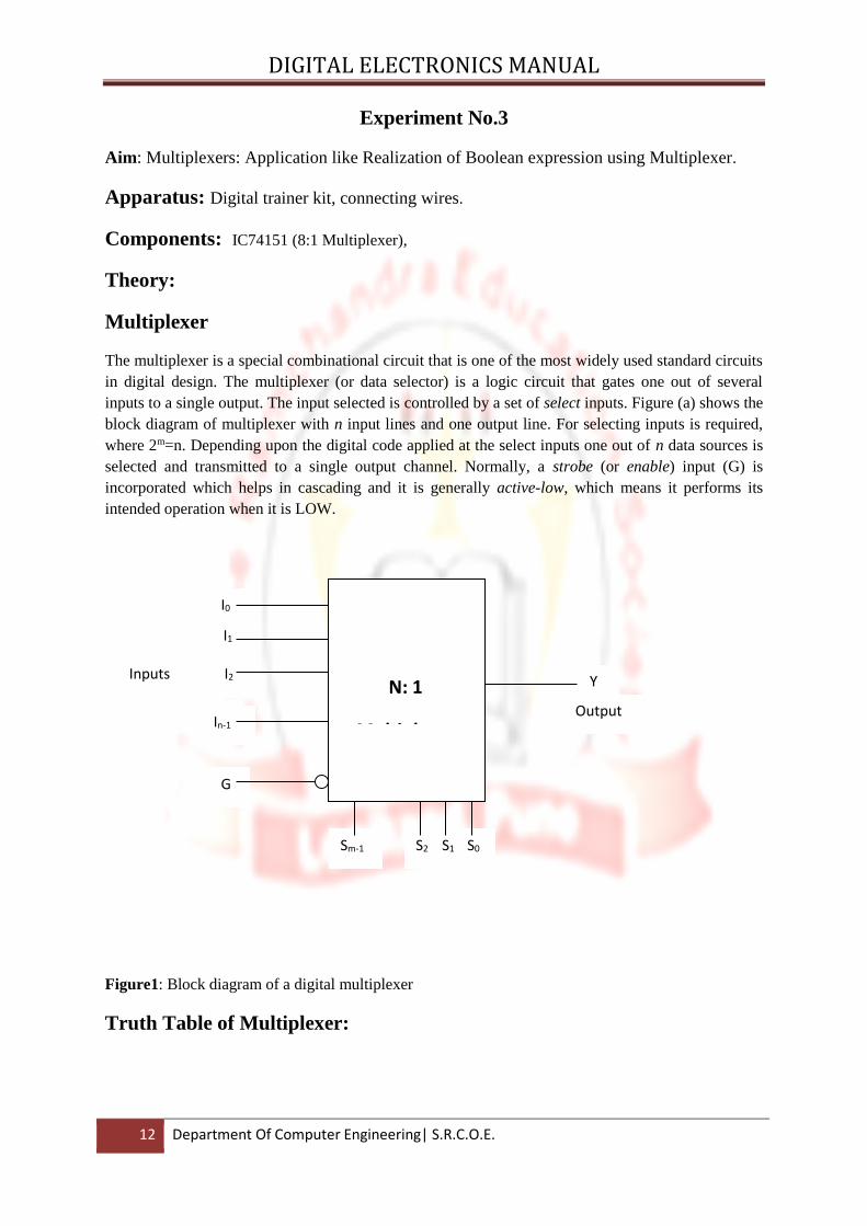
Experiment No.3
Aim: Multiplexers: Application like Realization of Boolean expression using Multiplexer.
Apparatus: Digital trainer kit, connecting wires.
Components: IC74151 (8:1 Multiplexer),
Theory:
Multiplexer
The multiplexer is a special combinational circuit that is one of the most widely used standard circuits
in digital design. The multiplexer (or data selector) is a logic circuit that gates one out of several
inputs to a single output. The input selected is controlled by a set of select inputs. Figure (a) shows the
block diagram of multiplexer with n input lines and one output line. For selecting inputs is required,
where 2m=n. Depending upon the digital code applied at the select inputs one out of n data sources is
selected and transmitted to a single output channel. Normally, a strobe (or enable) input (G) is
incorporated which helps in cascading and it is generally active-low, which means it performs its
intended operation when it is LOW.
Figure1: Block diagram of a digital multiplexer
Truth Table of Multiplexer:
Output
Y
Sm-1 S2 S1 S0
G
In-1
I2
I1
I0
Inputs
N: 1
Multiplexer
DIGITAL ELECTRONICS MANUAL
13 Department Of Computer Engineering| S.R.C.O.E.
Input
Select Inputs Enable Output
I0 0 0 0 0 I0
I1 0 0 1 0 I1
I2 0 1 0 0 I2
I3 0 1 1 0 I3
I4 1 0 0 0 I4
I5 1 0 1 0 I5
I6 1 1 0 0 I6
I7 1 1 1 0 I7
Types of Multiplexer:
o 2:1 MUX
o 4:1 MUX
o 8:1 MUX
o 16:1MUX
Different Multiplexer IC’s:
Implementation of combinational circuits using Multiplexer:
1. f (A,B,C) = m (0,1,2,4,5,6,14,15) using 8:1 MUX (IC 74151)
IC no. Description Output
74157 Quad 2:1 MUX Same as input
74158 Quad 2:1 MUX Inverted input
74153 Dual 4:1 MUX Same as input
74151A 8:1 MUX Complementary outputs
74152 8:1 MUX Inverted inputs
74150 16:1 MUX Inverted input
DIGITAL ELECTRONICS MANUAL
14 Department Of Computer Engineering| S.R.C.O.E.
2. f (A,B,C,D) = m (1,3,5,7) using 8:1 MUX (IC 74151)
3. f (A,B,C,D) = m (1,3,4,11,12,13,14,15) using 8:1 MUX (IC 74151)
Advantages of Multiplexer:
1. It reduces number of wires.
2. It reduces the circuit complexity and cost.
3. We can implement many combinational circuits.
4. It simplifies the logic design
5. It doesn’t need the k maps and simplification
Applications of Multiplexer:
1. Used as a data selector to select one out of many data inputs.
2. Used for simplification of logic design.
3. In data acquisition system
4. In designing the combinational circuits.
5. In D/A converters.
6. To minimize the number of connections
DIGITAL ELECTRONICS MANUAL
15 Department Of Computer Engineering| S.R.C.O.E.
Experiment No.4
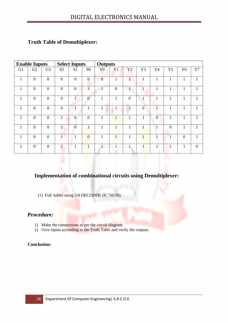
Aim: Demultiplexers: Applications like Realization of ROM using Demultiplexer
Implementation of combinational circuits using Demultiplexer:
(1) Full Adder using 3:8 DECODER (IC 74138)
Procedure:
1) Make the connections as per the circuit diagram.
2) Give inputs according to the Truth Table and verify the outputs.
Conclusion:
DIGITAL ELECTRONICS MANUAL
17 Department Of Computer Engineering| S.R.C.O.E.
Experiment No.5
Aim: BCD adder/Subtractor using 4 bit binary adder 7483
Apparatus: Digital trainer kit, connecting wires.
Components: IC7483, Logic Gates
Theory:
BCD adder is a circuit that adds 2 BCD digits and procedures a sum of digit also in BCD. BCD
addition procedures can be summarized as follows,
1. Add 2 BCD number using binary addition.
2. If the 4-bit sum is greater than 9 or if carry is generated, the sum is invalid. To correct the sum,
add 0110 to sum if carry is generated from this addition, add it to the next higher order BCD digit.
3. If the 4-bit sum is less than 9 or equal to 9, the sum is in proper BCD form.
Thus, to implement BCD adder we require:
1. A 4-bit binary adder for initial addition.
2. Logic circuits to detect sum greater than 9.
3. Another 4-bit adder to add 0110 in the sum if the sum is greater than 9 or carry is 1.
The logic circuit to determine sum greater than ‘9’ can be determined by simplifying the Boolean
expression of the given truth table: -
Design of BCD Adder using IC 7483:
As shown in figure the BCD number are first added in the top 4-bit binary adder to produce a
binary sum. When sum is greater than equal to 9 and Cout =0) nothing (i.e. zero) is added to the
binary sum. When it is equal to 1 (i.e. when a sum greater than 9 or Cout=1) binary 0110 is added to
the binary sum. The output generated from the bottom binary adder can be ignored, since it supplies
information already available at the output carry terminal.
DIGITAL ELECTRONICS MANUAL
18 Department Of Computer Engineering| S.R.C.O.E.
Fig1: Pin diagram of IC 7483 (Binary Adder).
A2
GND
S1
A1
B1
C0
C4
S4
B4
VCC
B2
S2
A4
S3
A3
B3
1
2
5
4
3
16
15
14
13
11
12
10
9 8
7
6
DIGITAL ELECTRONICS MANUAL
19 Department Of Computer Engineering| S.R.C.O.E.
Truth Table:
BCD SUM CARRY
S4 S3 S2 S1 C
0 0 0 0 0
0 0 0 1 0
0 0 1 0 0
0 0 1 1 0
0 1 0 0 0
0 1 0 1 0
0 1 1 0 0
0 1 1 1 0
1 0 0 0 0
1 0 0 1 0
1 0 1 0 1
1 0 1 1 1
1 1 0 0 1
1 1 0 1 1
1 1 1 0 1
1 1 1 1 1
DIGITAL ELECTRONICS MANUAL
20 Department Of Computer Engineering| S.R.C.O.E.
Y = S4 (S3 + S2)
Procedure:
(i) Make the connections as per circuit diagram.
(ii) Give any BCD number as input to the circuit
(iii) Observe the result of BCD addition at the output.
Results:
Conclusion:
DIGITAL ELECTRONICS MANUAL
21 Department Of Computer Engineering| S.R.C.O.E.
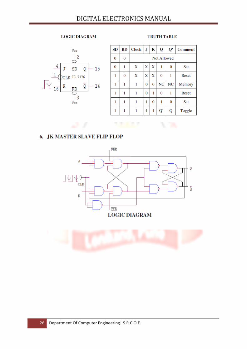
Experiment No.6
Aim: Flip flops, Registers and Counters (Study and Write up only).
Truth Table verification of
1) RS Flip Flop
2) T type Flip Flop.
3) D type Flip Flop.
4) JK Flip Flop.
5) JK Master Slave Flip Flop.
LEARNING OBJECTIVE:
_ To learn about various Flip-Flops
_ To learn and understand the working of Master slave FF
_ To learn about applications of FFs
_ Conversion of one type of Flip flop to another
COMPONENTS REQUIRED: IC 7408, IC 7404, IC 7402, IC 7400, Patch Cords & IC Trainer Kit.
THEORY:
Logic circuits that incorporate memory cells are called sequential logic circuits; their outputdepends
not only upon the present value of the input but also upon the previous values.Sequential logic circuits
often require a timing generator (a clock) for their operation.
The latch (flip-flop) is a basic bi-stable memory element widely used in sequential logic
circuits. Usually there are two outputs, Q and its complementary value.
Some of the most widely used latches are listed below.
SR LATCH:
An S-R latch consists of two cross-coupled NOR gates. An S-R flip-flop can also be design
using cross-coupled NAND gates as shown. The truth tables of the circuits are shown below.
A clocked S-R flip-flop has an additional clock input so that the S and R inputs are
active only when the clock is high. When the clock goes low, the state of flip-flop is latched
and cannot change until the clock goes high again. Therefore, the clocked S-R flip-flop
is also called “enabled” S-R flip-flop.
A D latch combines the S and R inputs of an S-R latch into one input by adding an
inverter. When the clock is high, the output follows the D input, and when the clock
goes low, the state is latched.
A S-R flip-flop can be converted to T-flip flop by connecting S input to Qb and R to Q.
DIGITAL ELECTRONICS MANUAL
22 Department Of Computer Engineering| S.R.C.O.E.
DIGITAL ELECTRONICS MANUAL
23 Department Of Computer Engineering| S.R.C.O.E.
DIGITAL ELECTRONICS MANUAL
24 Department Of Computer Engineering| S.R.C.O.E.
DIGITAL ELECTRONICS MANUAL
25 Department Of Computer Engineering| S.R.C.O.E.
DIGITAL ELECTRONICS MANUAL
26 Department Of Computer Engineering| S.R.C.O.E.
DIGITAL ELECTRONICS MANUAL
27 Department Of Computer Engineering| S.R.C.O.E.
Conclusion
DIGITAL ELECTRONICS MANUAL
28 Department Of Computer Engineering| S.R.C.O.E.
EXPERIMENT: 7
AIM :To implement the ripple counter using flip flop .
Theory: A counter is a sequential circuit that moves through a predefined sequence of states upon applying of clock pulses. The sequence of states may follow the binary number sequence or an arbitrary manner (no sequence). The simplest example of a counter is the binary counter which follows the binary number sequence. An n-bit binary counter contains n flip-flops and can count binary numbers from 0 to (2n -1). Counters are classified into two types: synchronous counters and ripple counter. In a synchronous counter, all flip flops are triggered by a common pulse (CP). In the ripple counter a flip flop output used as a signal for triggering other flip flop. In this experiment we will present these two types and explain their design and operation.
DIGITAL ELECTRONICS MANUAL
29 Department Of Computer Engineering| S.R.C.O.E.
Equipments: 1.4 J-K flip-flops (2 x 7473 TTL – IC chip) . 2.Logic Lab Trainer. 3.Connection leads.
Procedures: 1.Derive the wiring diagram for shown logic diagram. 2.Insure that the power switch of the IC trainer is turned off. 3.Plug the IC chips into the proper sockets. 4.Connect the voltage supply and ground lines to the chips. 5.Use the wires to connect the outputs of one IC to the input of another ICs according to the derived wiring diagram, try to work from left to right. 6.Once all connections have been done, turn on the power switch of the IC trainer. 7.Clear the flip-flops by applying logic '0' to the clear input. 8.Enable the counter and observe its function with each negative transition of clock pulse. 9.After finishing the experiment, turn off the power switch, disconnect the wires and take out all of the IC chips from the trainer.
Conclusion:
DIGITAL ELECTRONICS MANUAL
30 Department Of Computer Engineering| S.R.C.O.E.
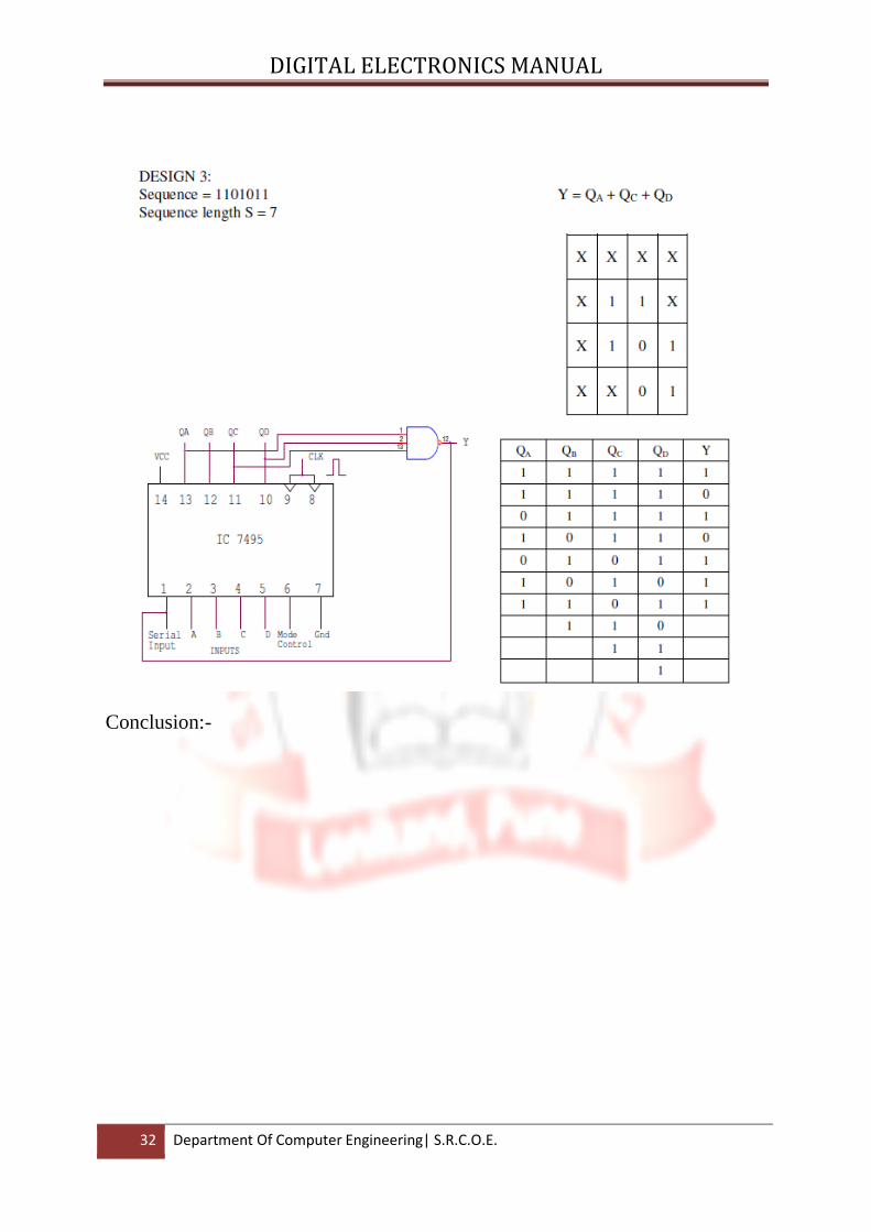
EXPERIMENT: 8
AIM: Design and set up a Sequence Generator using IC 7495. COMPONENTS REQUIRED: IC 7495, IC 7486, Patch Cords & IC Trainer Kit. PROCEDURE:
1. Check all the components for their working. 2. Insert the appropriate IC into the IC base. 3. Make connections as shown in the circuit diagram. 4. By Keeping mode=1. Load the input A,B,C,D as in Truth Table 1st Row and give a
clock
5. pulseFor count mode make mode = 0.
6. Verify the Truth Table and observe the outputs. DESIGN 1: Sequence = 100010011010111 Sequence length S = 15 Y = QC (+) QD
DIGITAL ELECTRONICS MANUAL
31 Department Of Computer Engineering| S.R.C.O.E.
DIGITAL ELECTRONICS MANUAL
32 Department Of Computer Engineering| S.R.C.O.E.
Conclusion:-
DIGITAL ELECTRONICS MANUAL
33 Department Of Computer Engineering| S.R.C.O.E.
EXPERIMENT: 9 AIM: To design IC 74193 as a up/down counter LEARNING OBJECTIVE: To learn about Up- Down Counter and its application COMPONENTS REQUIRED: IC 74193, Patch Cords & IC Trainer Kit PROCEDURE:
Check all the components for their working.
Insert the appropriate IC into the IC base.
Make connections as shown in the circuit diagram.
Verify the Truth Table and observe the outputs.
PIN DETAILS OF IC 74193
DIGITAL ELECTRONICS MANUAL
34 Department Of Computer Engineering| S.R.C.O.E.
DIGITAL ELECTRONICS MANUAL
35 Department Of Computer Engineering| S.R.C.O.E.
DIGITAL ELECTRONICS MANUAL
36 Department Of Computer Engineering| S.R.C.O.E.
DIGITAL ELECTRONICS MANUAL
37 Department Of Computer Engineering| S.R.C.O.E.
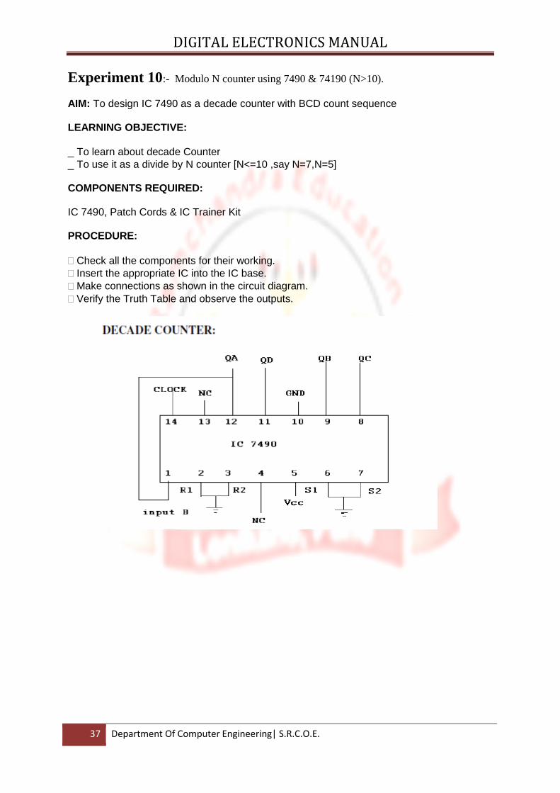
Experiment 10:- Modulo N counter using 7490 & 74190 (N>10).
AIM: To design IC 7490 as a decade counter with BCD count sequence LEARNING OBJECTIVE:
_ To learn about decade Counter
_ To use it as a divide by N counter [N<=10 ,say N=7,N=5] COMPONENTS REQUIRED: IC 7490, Patch Cords & IC Trainer Kit PROCEDURE:
Check all the components for their working.
Insert the appropriate IC into the IC base.
Make connections as shown in the circuit diagram.
Verify the Truth Table and observe the outputs.
DIGITAL ELECTRONICS MANUAL
38 Department Of Computer Engineering| S.R.C.O.E.
DIGITAL ELECTRONICS MANUAL
39 Department Of Computer Engineering| S.R.C.O.E.
DIGITAL ELECTRONICS MANUAL
40 Department Of Computer Engineering| S.R.C.O.E.
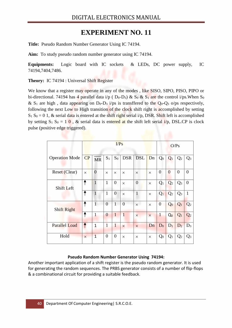
EXPERIMENT NO. 11
Title: Pseudo Random Number Generator Using IC 74194.
Aim: To study pseudo random number generator using IC 74194.
Equipments: Logic board with IC sockets & LEDs, DC power supply, IC
74194,7404,7486.
Theory: IC 74194 : Universal Shift Register
We know that a register may operate in any of the modes , like SISO, SIPO, PISO, PIPO or
bi-directional. 74194 has 4 parallel data i/p ( D0-D3) & S0 & S1 are the control i/ps.When S0
& S1 are high , data appearing on D0-D3 i/ps is transffered to the Q0-Q3 o/ps respectively,
following the next Low to High transition of the clock shift right is accomplished by setting
S1 S0 = 0 1, & serial data is entered at the shift right serial i/p, DSR. Shift left is accomplished
by setting S1 S0 = 1 0 , & serial data is entered at the shift left serial i/p, DSL.CP is clock
pulse (positive edge triggered).
Operation Mode
I/Ps
O/Ps
CP
MR S1 S0 DSR DSL Dn Q0 Q1 Q2 Q3
Reset (Clear) 0 0 0 0 0
Shift Left
1 1 0 0 Q1 Q2 Q3 0
1 1 0 1 Q1 Q2 Q3 1
Shift Right
1 0 1 0 0 Q0 Q1 Q2
1 0 1 1 1 Q0 Q1 Q2
Parallel Load 1 1 1 Dn D0 D1 D2 D3
Hold 1 0 0 Q0 Q1 Q2 Q3
Pseudo Random Number Generator Using 74194: Another important application of a shift register is the pseudo random generator. It is used for generating the random sequences. The PRBS generator consists of a number of flip-flops & a combinational circuit for providing a suitable feedback.
DIGITAL ELECTRONICS MANUAL
41 Department Of Computer Engineering| S.R.C.O.E.
Q3 Q2 Q1 Q0 = 0 0 1 1
The PRBS generator cannot generate a truly random sequence because this stucture is a deterministic stucture. This is the reason why the sequence repeats itself. The maximum length of the sequence will be 2m-1.This is because the state 0 0 0…….0 must be excluded.
Binary sequence of Q3
Length of PRBS : 2m-1
For m=4 : 24-1 =15
PRBS sequence repeats itself after every 15 clock cycles.
Clock Pulse Number
Shift Register Ex-OR gate
PRBS Sequence
Q3 Q2 Q1 Q0 Q3 Q2 Q3
0 0 0 1 1 0 0=0 0
1 0 1 1 0 0 1=1 0
2 1 1 0 1 1 1=0 1
3 1 0 1 0 1 0=1 1
4 0 1 0 1 0 1=1 0
5 1 0 1 1 1 0=1 1
6 0 1 1 1 0 1=1 0
7 1 1 1 1 1 1=0 1
8 1 1 1 0 1 1=0 1
9 1 1 0 0 1 1=0 1
10 1 0 0 0 1 0=1 1
11 0 0 0 1 0 0=0 0
12 0 0 1 0 0 0=0 0
13 0 1 0 0 0 1=1 0
14 1 0 0 1 1 0=1 1
15 0 0 1 1 0 0=0 0
16 0 1 1 0 0 1=1 0
17 1 1 0 1 1 1=0 1
0 0 1 1 0 1 0 1 1 1 1 0 0 0 1
DIGITAL ELECTRONICS MANUAL
42 Department Of Computer Engineering| S.R.C.O.E.
Application of PRBS:
Since the sequence produced is random, PRBS generator is also called as a Pseudo
Noise Generator. This noise can be used to test the noise immunity of the system
under test.
PRBS generator is an important part of data encryption system. Such a system is
required to protect the data from data hackers.
Procedure:
1) Adjust data o/p of Q3 Q2 Q1 Q0 = 0 0 1 1 using parallel load operation mode.
2) Connect EX-OR gate o/p to DSR pin of IC 74194 & i/p for EX-OR Q2 & Q3.
3) Apply nagative clock pulse to pin-11 of IC 74194 & press trigger button to get
PRB sequence at Q3 o/p pi-12 of IC 74194.
Method-II
Shift right operation mode of IC 74194.
Connect MR pin to ground . All o/p of Q0 Q1 Q2 Q3 = 0 0 0 0.
Then shift right operation mode.
Clock
Pulse
Shift Register EX-NOR
Gate
PRB
Sequence
Q3 Q2 Q1 Q0 Q3
0 0 0 0 0 0 0 = 1 0
1 0 0 0 1 0 0 = 1 0
2 0 0 1 1 0 0 = 1 0
3 0 1 1 1 0 1 = 0 0
4 1 1 1 0 1 1 = 1 1
5 1 1 0 1 1 1 = 1 1
6 1 0 1 1 1 0 = 0 1
7 0 1 1 0 0 1 = 0 0
8 1 1 0 0 1 1 = 1 1
DIGITAL ELECTRONICS MANUAL
43 Department Of Computer Engineering| S.R.C.O.E.
9 1 0 0 1 1 0 = 0 1
10 0 0 1 0 0 0 = 1 0
11 0 1 0 1 0 1 = 0 0
12 1 0 1 1 1 0 = 0 1
13 0 1 0 0 0 1 = 0 0
14 1 0 0 0 1 0 = 0 1
15 0 0 0 0 0 0 = 1 0
16 0 0 0 1 0 0 = 1 0
17 0 0 1 1 0 0 = 1 0
18 0 1 1 1 0 1 = 0 0
19 1 1 1 0 1 1 = 1 1
Procedure:
1. First reset all flip-flops of IC 74194 i.e. Q3 Q2 Q1 Q0 = 0 0 0 0.
2. Shift right operation mode .
3. Connect EX-NOR means o/p of EX-OR is connected to OR gate & OR gate o/p is
connected to DSR.
Conclusion: Pseudo random generator successfully implemented.
DIGITAL ELECTRONICS MANUAL
44 Department Of Computer Engineering| S.R.C.O.E.
****Experiment No 11 Introduction to VHDL DESIGN FLOW (VHDL Code)
Create a New Project
Create a new ISE project which will target the FPGA device on the Spartan-3 Startup Kit demo board.
To create a new project:
1. Select File New Project... The New Project Wizard appears.
2. Type tutorial in the Project Name field.
3. Enter or browse to a location (directory path) for the new project. A tutorial
subdirectory is created automatically.
4. Verify that HDL is selected from the Top-Level Source Type list.
5. Click Next to move to the device properties page.
6. Fill in the properties in the table as shown below:
Product Category: All
Family: Spartan3
Device: XC3S200
Package: PQ208
Speed Grade: -4
Top-Level Module Type: HDL
Synthesis Tool: XST (VHDL/Verilog)
Simulator: ISE Simulator (VHDL/Verilog)
Verify that Enable Enhanced Design Summary is selected.
Leave the default values in the remaining fields.
When the table is complete, your project properties will look like the following:
Figure 2: Project Device Properties
DIGITAL ELECTRONICS MANUAL
45 Department Of Computer Engineering| S.R.C.O.E.
7. Click Next to proceed to the Create New Source window in the New Project Wizard. At the end of
the next section, your new project will be complete.
Creating a VHDL Source
Create a VHDL source file for the project as follows:
1. Click the New Source button in the New Project Wizard.
2. Select VHDL Module as the source type.
3. Type in the file name counter.
4. Verify that the Add to project checkbox is selected.
5. Click Next.
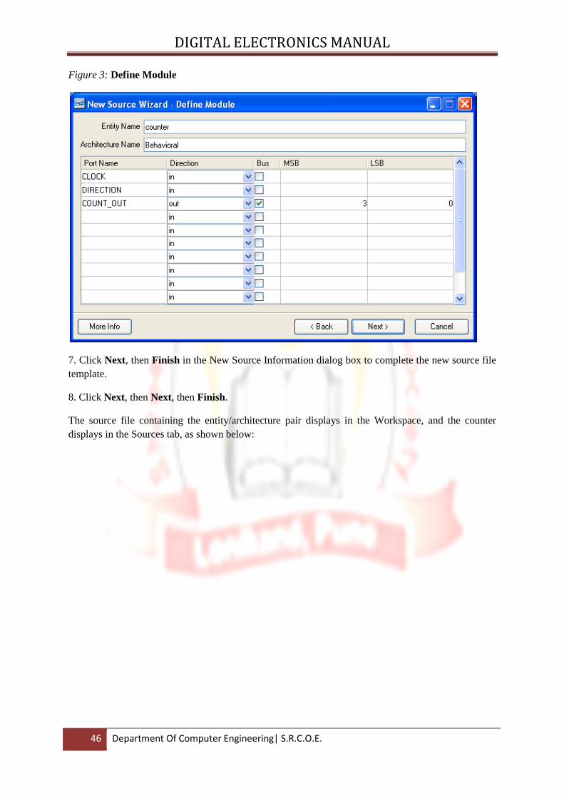
6. Declare the ports for the counter design by filling in the port information as shown
below:
7. Click Next, then Finish in the New Source Information dialog box to complete the new source file
template.
8. Click Next, then Next, then Finish.
DIGITAL ELECTRONICS MANUAL
46 Department Of Computer Engineering| S.R.C.O.E.
Figure 3: Define Module
7. Click Next, then Finish in the New Source Information dialog box to complete the new source file
template.
8. Click Next, then Next, then Finish.
The source file containing the entity/architecture pair displays in the Workspace, and the counter
displays in the Sources tab, as shown below:
DIGITAL ELECTRONICS MANUAL
47 Department Of Computer Engineering| S.R.C.O.E.
When you are finished, the counter source file will look like the following:
library IEEE;
use IEEE.STD_LOGIC_1164.ALL;
use IEEE.STD_LOGIC_ARITH.ALL;
use IEEE.STD_LOGIC_UNSIGNED.ALL;
-- Uncomment the following library declaration if instantiating
-- any Xilinx primitive in this code.
--library UNISIM;
--use UNISIM.VComponents.all;
entity counter is
Port ( CLOCK : in STD_LOGIC;
DIGITAL ELECTRONICS MANUAL
48 Department Of Computer Engineering| S.R.C.O.E.
DIRECTION : in STD_LOGIC;
COUNT_OUT : out STD_LOGIC_VECTOR (3 downto 0));
end counter;
architecture Behavioral of counter is
signal count_int : std_logic_vector(3 downto 0) := "0000";
begin
process (CLOCK)
begin
if CLOCK='1' and CLOCK'event then
if DIRECTION='1' then
count_int <= count_int + 1;
else
count_int <= count_int - 1;
end if;
end if;
end process;
COUNT_OUT <= count_int;
end Behavioral;
Checking the Syntax of the New Counter Module
When the source files are complete, check the syntax of the design to find errors and typos.
1. Verify that Synthesis/Implementation is selected from the drop-down list in the
Sources window.
2. Select the counter design source in the Sources window to display the related
processes in the Processes window.
3. Click the “+” next to the Synthesize-XST process to expand the process group.
DIGITAL ELECTRONICS MANUAL
49 Department Of Computer Engineering| S.R.C.O.E.
4. Double-click the Check Syntax process.
Note: You must correct any errors found in your source files. You can check for errors in the Console
tab of the Transcript window. If you continue without valid syntax, you will not be able to simulate or
synthesize your design.
5. Close the HDL file.
Design Simulation
Verifying Functionality using Behavioral Simulation
Create a test bench waveform containing input stimulus you can use to verify the functionality of the
counter module. The test bench waveform is a graphical view of a test bench.
Create the test bench waveform as follows:
1. Select the counter HDL file in the Sources window.
2. Create a new test bench source by selecting Project → New Source.
3. In the New Source Wizard, select Test Bench WaveForm as the source type, and type
counter_tbw in the File Name field.
4. Click Next.
5. The Associated Source page shows that you are associating the test bench waveform
with the source file counter. Click Next.
6. The Summary page shows that the source will be added to the project, and it displays the source
directory, type and name. Click Finish.
7. You need to set the clock frequency, setup time and output delay times in the Initialize Timing
dialog box before the test bench waveform editing window opens.
DIGITAL ELECTRONICS MANUAL
50 Department Of Computer Engineering| S.R.C.O.E.
EXPERIMENT NO. 14
TITLE: 4-bit Asynchronous down counter using VHDL.
Aim: Study of 4-bit Asynchronous down counter using VHDL.
Theory: VHDL Statements:
There are two classes of statements you can use in your VHDL descriptions:
• Sequential statements
• Concurrent statements
Fig. A VHDL Statements
A VHDL architecture construct comprises a set of interconnected concurrent statements, such
as processes and blocks, which describe an overall design in terms of behavior or structure.
Concurrent statements in a design execute simultaneously, unlike sequential statements,
which execute one after another.
Sequential Statements:
A set of VHDL statement that executes. in sequence is called sequential statements.
Sequential statements can appear only in processes and subprograms. You can use sequential
statements only inside a process statement or within a subprogram (procedure or function).
Each statement executes in the order in which it is encountered. The preceding BNF
description listed the sequential statements available in VHDL.
Sequential statements are divided into categories, based on their operation. The following list
shows the categories for the sequential statements:
The types of sequential statements are:
DIGITAL ELECTRONICS MANUAL
51 Department Of Computer Engineering| S.R.C.O.E.
• Assignment Statements and Targets
• Variable Assignment Statements
• Signal Assignment Statements
• If Statements
• Case Statements
• Loop Statements
• Next Statements
• Exit Statements
• Subprograms
• Return Statement
• Wait Statements
• Null Statements
Concurrent Statements:
The functionality of a design is defined in VHDL by a set of concurrent statements.
These statements mimic hardware in that many of these statements can be active at the same
time. All concurrent statements describe the functionality of multiplexer structures. It is
impossible to model storage elements, like Flip Flops with concurrent statements, only.
The main concurrent statements:
1. Process Statements
2. Block Statements
Concurrent Versions of Sequential Statements:
1. Concurrent Procedure Calls
2. Concurrent Signal Assignments
3. Component Instantiation Statements
4. Direct Instantiation
5. Generate Statements
DIGITAL ELECTRONICS MANUAL
52 Department Of Computer Engineering| S.R.C.O.E.
Process Statements:
A process statement (which is concurrent) contains a set of sequential statements.
Although all processes in a design execute concurrently, the sequential statements within
each process one at a time.A process communicates with the rest of the design by reading
values from or writing them to signals or ports outside the process.The process statement in
VHDL is the primary means by which sequential operations (such as registered circuits) can
be described.
The process statement represents the behavior of some portion of the design. It
consists of the sequential statements whose execution is made in order defined by the user.
Each process can be assigned an optional label. The process declarative part defines local
items for the process and may contain declarations of: subprograms, types, subtypes,
constants, variables, files, aliases, attributes, use clauses and group declarations. It is not
allowed to declare signals or shared variables inside processes.
The statements, which describe the behavior in a process, are executed sequentially,
in the order in which the designer specifies them. The execution of statements however does
not terminate with the last statement in the process, but is repeated in an infinite loop.
1.Assignment Statements and Targets:
Use an assignment statement to assign a value to a variable or signal.
The syntax is:
target := expression; -- Variable assignment
target <= expression; --Signal assignment
Target:
The target can be a variable or a signal (or part of a variable or a signal, such as a sub
array) that receives the value of the expression. The expression must evaluate to the same
type as the target.
The difference in syntax between variable assignments and signal assignments is that
— Variables use the: = operator
Variables are local to a process or subprogram, and their assignments take effect
immediately.
— Signals use the <= operator
Signals need to be global in a process or subprogram, and their assignments take effect at the
end of a process. Signals are the only means of communication between processes.
1.1 Variable Assignment Statements:
A variable assignment changes the value of a variable.
DIGITAL ELECTRONICS MANUAL
53 Department Of Computer Engineering| S.R.C.O.E.
The syntax is:
target: — expression;
Target:
Names the variables that receive the value of expression.
Expression:
Determines the assigned value; its type must be compatible with the target.
When a variable is assigned a value, the assignment takes place immediately. A variable
keeps its assigned value until another assignment takes place.
1.2 Signal Assignment Statements:
A signal assignment changes the value being driven on a signal by the current process.
The syntax is:
target <= expression;
Target:
Names the signals that receive the value of expression.
Expression
Determines the assigned value; its type must be compatible with target.
Signals and variables act in different ways when they receive values. The differences lie in
the way the two kinds of assignments take effect and how that influence the value reads from
either variables or signals.
2. IF Statements:
The if statement is a statement that depending on the value of one or more
corresponding conditions, selects for execution one or none of the enclosed sequences of
statements.
The syntax is:
1) if-then statement
if condition then
sequential_statements
end if;
2) if-then-else statement
if condition then
sequentiaL_statements
DIGITAL ELECTRONICS MANUAL
54 Department Of Computer Engineering| S.R.C.O.E.
else
sequential_statements
end if;
3) if-then-elsif-else statement
if condition then
sequential_statements
eLsif condition then
sequential_statements
else
sequential_statements
end if;
3.Case Statements:
Definition:
The case statement selects for execution one of several alternative sequences of
statements; the alternative is chosen based on the value of the associated expression.
The syntax is:
case expression is
when choices =>
{ sequentiaL_statement }
{ when choices =>
{ sequentiaL_statement } }
end case;
4.Loop Statements:
Definition:
A loop statement repeatedly executes a sequence of statements.
The syntax is:
[ Label: ] [ iteration_scheme]loop
{ sequential_statement }
{ next [ tabel] [ when condition ] ; }
DIGITAL ELECTRONICS MANUAL
55 Department Of Computer Engineering| S.R.C.O.E.
{ exit [ label] [ condition ] ; }
end Loop [label];
5.For---Loop Statements
The for loop is a sequential statement that allows you to specify a fixed number of
iterations in a behavioral design description. The for loop includes an automatic declaration
for the index (i in following example). You do not need to separately declare the index
variable.
The syntax is:
[label:] for identifier in range Loop
{ sequential_ statement }
end loop [label]
6. Next Statements:
The next statement allows skipping a part of an iteration loop. If the condition
specified after the when reserved word is TRUE, or if there is no condition at all, then the
statement is executed.
The syntax is:
next [label] [ when condition ];
7. Exit Statements:
The exit statement completes execution of an enclosing iôop statement, called label in
the syntax. The completion is conditional if the statement includes a condition, such as the
when condition.
The execution of the exit statement depends on a condition placed at the end of the
statement, right after the when reserved word. When the condition is TRUE (or if there is no
condition at all) the exit statement is executed and the control is passed to the first statement
after the end loop.
The syntax is:
exit [label] [when condition];
8. Return Statements:
The return statement ends the execution of a subprogram (procedure or function) in
which it appears. It causes an unconditional jump to the end of a subprogram.
The syntax is:
return expression ;. -- Functions
DIGITAL ELECTRONICS MANUAL
56 Department Of Computer Engineering| S.R.C.O.E.
return; -- Procedures
9. Null Statements:
The null statement explicitly states that no action is required. It is often used in case
statements because all choices must be covered, even if some of the choices are ignored.
The Syntax is:
null;
Example: Implement 4-bit binary asynchronous down counter.
The behavioral VHDL code for the 4-bit binary down counter is Shown in Fig.B
The statement USE IEEE.STD_LOGIC_UNSIGNED. ALL is needed in order to perform
subtractions on STD_LOGIC_VECTORs.
Fig.B 4-bit binary down counter
DIGITAL ELECTRONICS MANUAL
57 Department Of Computer Engineering| S.R.C.O.E.
Design Experiments:
1. Implement VHDL code for BCD Up-Down Counter.
2. Implement VHDL code for 00 to 99 Up-Down Counter.
3. Implement VHDL code for 4-bit ripple Up counter.