Power Electronics in Renewable Energy Systems A PROJECT REPORT On Harmonic comparisons of various PWM techniques for basic MLI Submitted by MD SAQUIB MAQSOOD M.Tech PED SRM UNIVERSITY, CHENNAI, INDIA
Transcript
Power Electronics in Renewable Energy Systems
A PROJECT REPORT
On
Harmonic comparisons of various PWM techniques
for basic MLI
Submitted by
MD SAQUIB MAQSOOD
M.Tech PED
SRM UNIVERSITY, CHENNAI, INDIA
Abstract: Cascaded inverters are ideal for connecting renewable energy sources with an AC
grid, because of the need for separate dc sources, which is the case in applications such as
photovoltaic or fuel cells. The inverter could be controlled to either regulate the power factor of
the current drawn from the source or the bus voltage of the electrical system where the inverter
was connected. The modulation techniques are crucial in operating any inverter at desired
conditions. In this paper different PWM techniques are implemented for five level cascaded
multilevel inverter and THD variation is analyzed.
INTRODUCTION:
A voltage level of three is considered to be the smallest number in multilevel converter
topologies. Due to the bi-directional switches, the multilevel VSC can work in both rectifier and
inverter modes. This is why most of the time it is referred to as a converter instead of an inverter
in this dissertation. A multilevel converter can switch either its input or output nodes (or both)
between multiple (more than two) levels of voltage or current. As the number of levels reaches
infinity, the output THD approaches zero. The number of the achievable voltage levels, however,
is limited by voltage-imbalance problems, voltage clamping requirements, circuit layout and
packaging constraints complexity of the controller, and, of course, capital and maintenance costs.
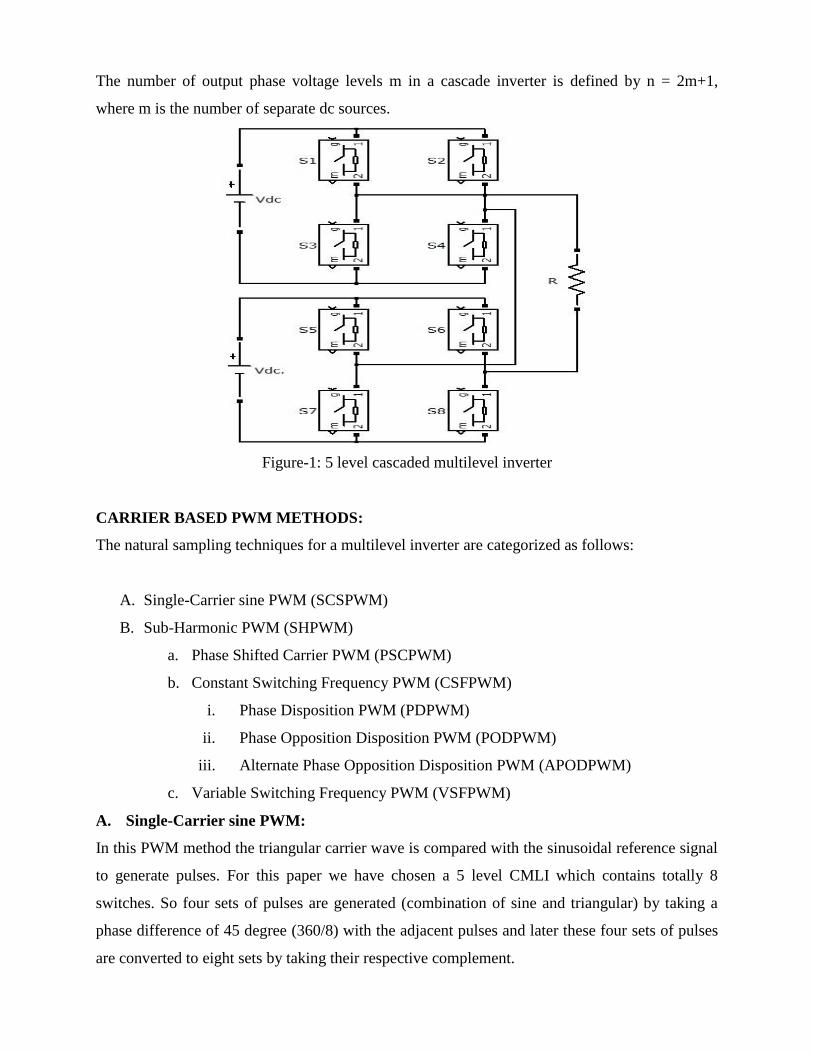
The MLI topology is based on the series connection of single-phase inverters with separate dc
sources. Fig. shows the power circuit for one phase leg of a three-level, five-level and seven-
level cascaded inverter. The resulting phase voltage is synthesized by the addition of the voltages
generated by the different cells. In a 3-level cascaded inverter each single-phase full-bridge
inverter generates three voltages at the output: +Vdc, 0, -Vdc (zero, positive dc voltage, and
negative dc voltage). This is made possible by connecting the capacitors sequentially to the ac
side via the power switches. The resulting output ac voltage swings from -Vdc to +Vdc with three
levels, -2Vdc to +2Vdc with five-level and -3Vdc to +3Vdc with seven-level inverter. The staircase
waveform is nearly sinusoidal, even without filtering. Each H bridge inverter level can generate
three different voltage outputs, +Vdc, 0, and –Vdc by connecting the dc source to the ac output by
different combinations of the four switches. To obtain +Vdc, switches S1 and S4 are turned on,
whereas – Vdc can be obtained by turning on switches S2 and S3. By turning on S1 and S2 or S3
and S4, the output voltage is 0. The ac outputs of each of the different full-bridge inverter levels
are connected in series such that the synthesized voltage waveform is the sum of the inverter
outputs.
The number of output phase voltage levels m in a cascade inverter is defined by n = 2m+1,
where m is the number of separate dc sources.
Figure-1: 5 level cascaded multilevel inverter
CARRIER BASED PWM METHODS:
The natural sampling techniques for a multilevel inverter are categorized as follows:
A. Single-Carrier sine PWM (SCSPWM)
B. Sub-Harmonic PWM (SHPWM)
a. Phase Shifted Carrier PWM (PSCPWM)
b. Constant Switching Frequency PWM (CSFPWM)
i. Phase Disposition PWM (PDPWM)
ii. Phase Opposition Disposition PWM (PODPWM)
iii. Alternate Phase Opposition Disposition PWM (APODPWM)
c. Variable Switching Frequency PWM (VSFPWM)
A. Single-Carrier sine PWM:
In this PWM method the triangular carrier wave is compared with the sinusoidal reference signal
to generate pulses. For this paper we have chosen a 5 level CMLI which contains totally 8
switches. So four sets of pulses are generated (combination of sine and triangular) by taking a
phase difference of 45 degree (360/8) with the adjacent pulses and later these four sets of pulses
are converted to eight sets by taking their respective complement.
Figure-2: SCSPWM generated pulses
B. Sub-Harmonic PWM (SHPWM):
Sub-Harmonic PWM is an exclusive control strategy for multilevel inverters and has further
classifications.
a. Phase Shifted Carrier PWM (PSPWM)
b. Constant Switching Frequency PWM (CSFPWM)
c. Variable Switching Frequency PWM (VSFPWM)
a. Phase Shifted Carrier PWM (PSCPWM):
All the triangular carriers have the same frequency and the same peak to peak amplitude. There
is a phase shift between any two adjacent carrier waves, given by
Øcr =
m= number of level, for m=5
Øcr = 360°/4
Øcr = 90°
Comparison of carrier and modulating waves for five level are shown in fig.3.
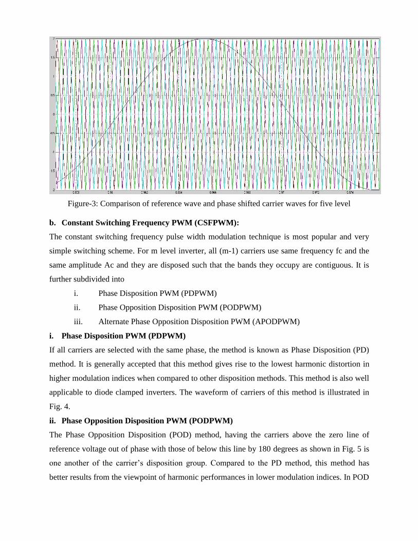
Figure-3: Comparison of reference wave and phase shifted carrier waves for five level
b. Constant Switching Frequency PWM (CSFPWM):
The constant switching frequency pulse width modulation technique is most popular and very
simple switching scheme. For m level inverter, all (m-1) carriers use same frequency fc and the
same amplitude Ac and they are disposed such that the bands they occupy are contiguous. It is
further subdivided into
i. Phase Disposition PWM (PDPWM)
ii. Phase Opposition Disposition PWM (PODPWM)
iii. Alternate Phase Opposition Disposition PWM (APODPWM)
i. Phase Disposition PWM (PDPWM)
If all carriers are selected with the same phase, the method is known as Phase Disposition (PD)
method. It is generally accepted that this method gives rise to the lowest harmonic distortion in
higher modulation indices when compared to other disposition methods. This method is also well
applicable to diode clamped inverters. The waveform of carriers of this method is illustrated in
Fig. 4.
ii. Phase Opposition Disposition PWM (PODPWM)
The Phase Opposition Disposition (POD) method, having the carriers above the zero line of
reference voltage out of phase with those of below this line by 180 degrees as shown in Fig. 5 is
one another of the carrier’s disposition group. Compared to the PD method, this method has
better results from the viewpoint of harmonic performances in lower modulation indices. In POD
method, there is no harmonic at the carrier frequency and its multiples and the dispersion of
harmonics occurs around them.
iii. Alternate Phase Opposition Disposition PWM (APODPWM)
The third member of the carriers’ disposition group is known as Alternative Phase Opposition
Disposition (APOD) method. Each carrier of this method is phase shifted by 180 degrees from its
adjacent one. It should be noted that POD and APOD methods are exactly the same for a 3-level
Inverter. This method gives almost the same results as the POD method. The major differences
are the larger amount of third order harmonics which is not important because of their
cancellation in line voltages. Thus, this method results in a better THD for line voltages when
comparing to the POD method. The carrier waveforms of this method are illustrated in Fig 6.
Figure 4: Comparison of reference wave and phase disposition carrier waves for five level
Figure 5: Comparison of reference wave and phase opposition disposition carrier waves
Figure 6: Comparison of reference wave and alternate phase opposition disposition carrier waves
c. Variable Switching Frequency PWM (VSFPWM):
The number of switching for upper and lower devices is much more than that of intermediate
switches in constant switching frequency carriers. In order to equalize the number of switching
for all switches, variable frequency PWM is used. Here the carrier sets C1 and C4 will have the
same frequencies, C2 and C3 will have the same frequencies. Fig.7 shows the multicarrier signal
for variable switching frequency PWM.
Figure 7: Comparison of reference wave and variable frequency disposition carrier waves
SIMULATION CIRCUITS FOR DIFFERENT PWM:
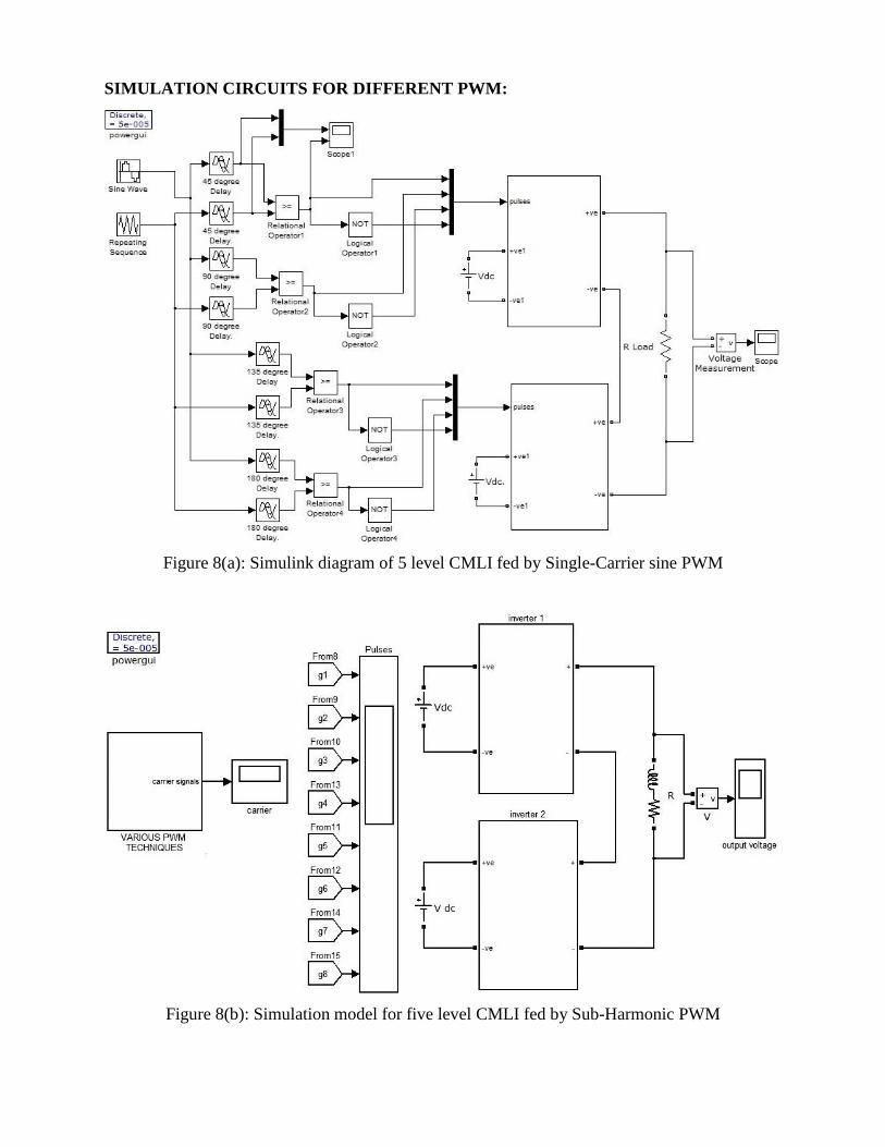
Figure 8(a): Simulink diagram of 5 level CMLI fed by Single-Carrier sine PWM
Figure 8(b): Simulation model for five level CMLI fed by Sub-Harmonic PWM
Figure 8(c): Simulation model for PSCPWM
Figure 8(d): Simulation model for PDPWM
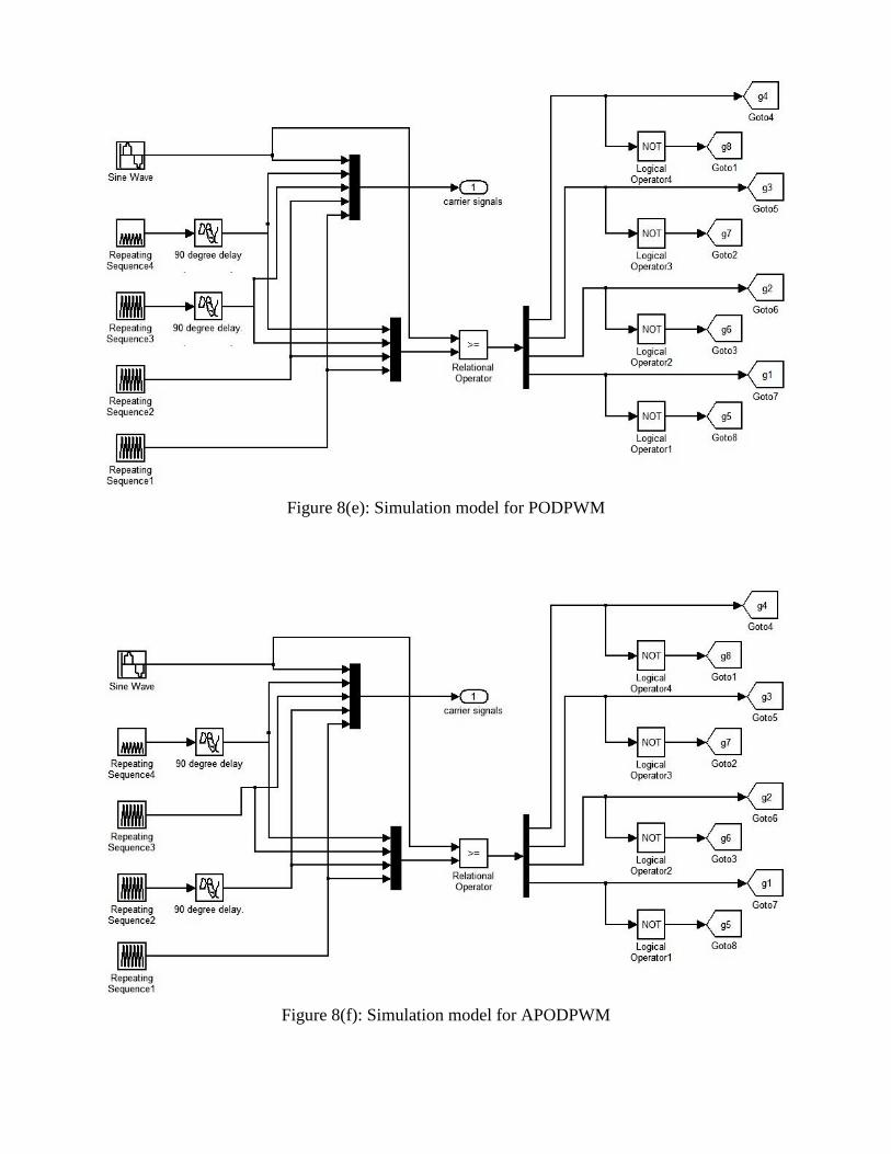
Figure 8(e): Simulation model for PODPWM
Figure 8(f): Simulation model for APODPWM
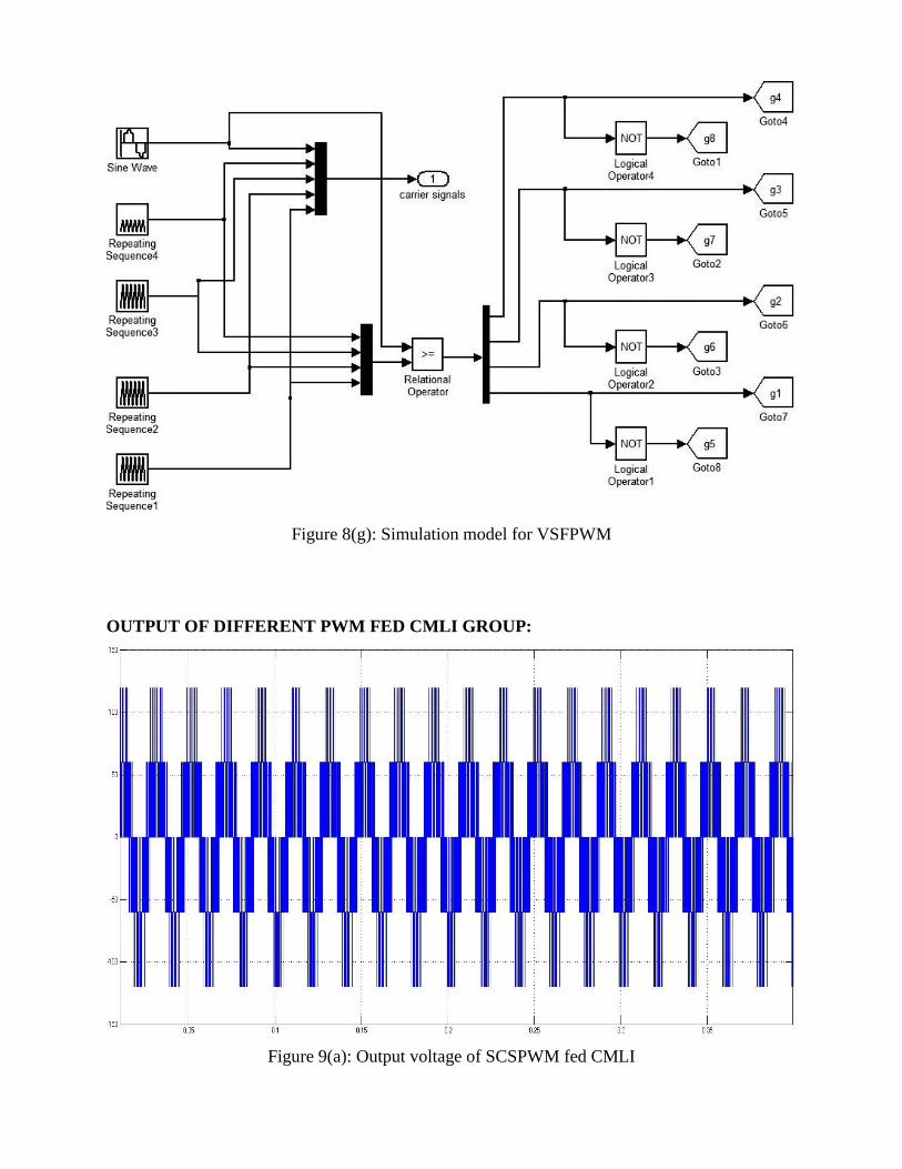
Figure 8(g): Simulation model for VSFPWM
OUTPUT OF DIFFERENT PWM FED CMLI GROUP:
Figure 9(a): Output voltage of SCSPWM fed CMLI
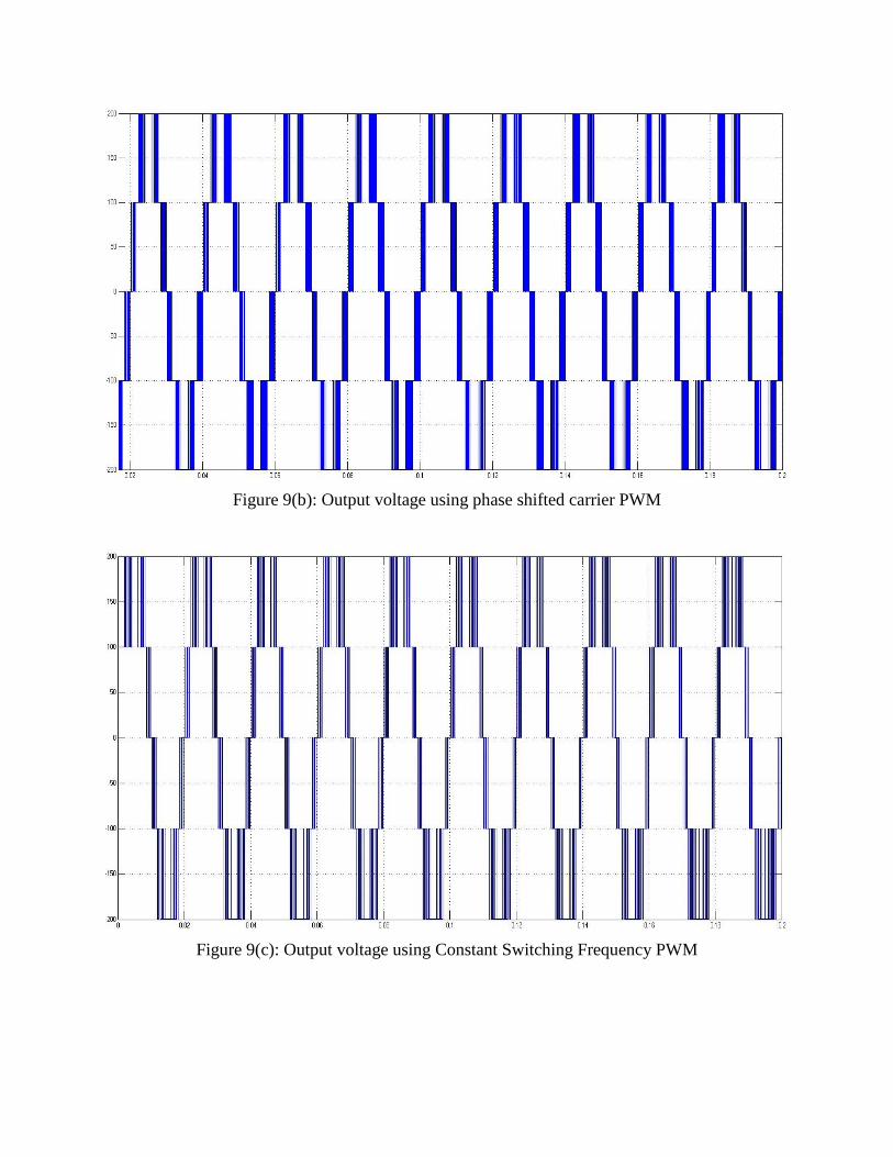
Figure 9(b): Output voltage using phase shifted carrier PWM
Figure 9(c): Output voltage using Constant Switching Frequency PWM
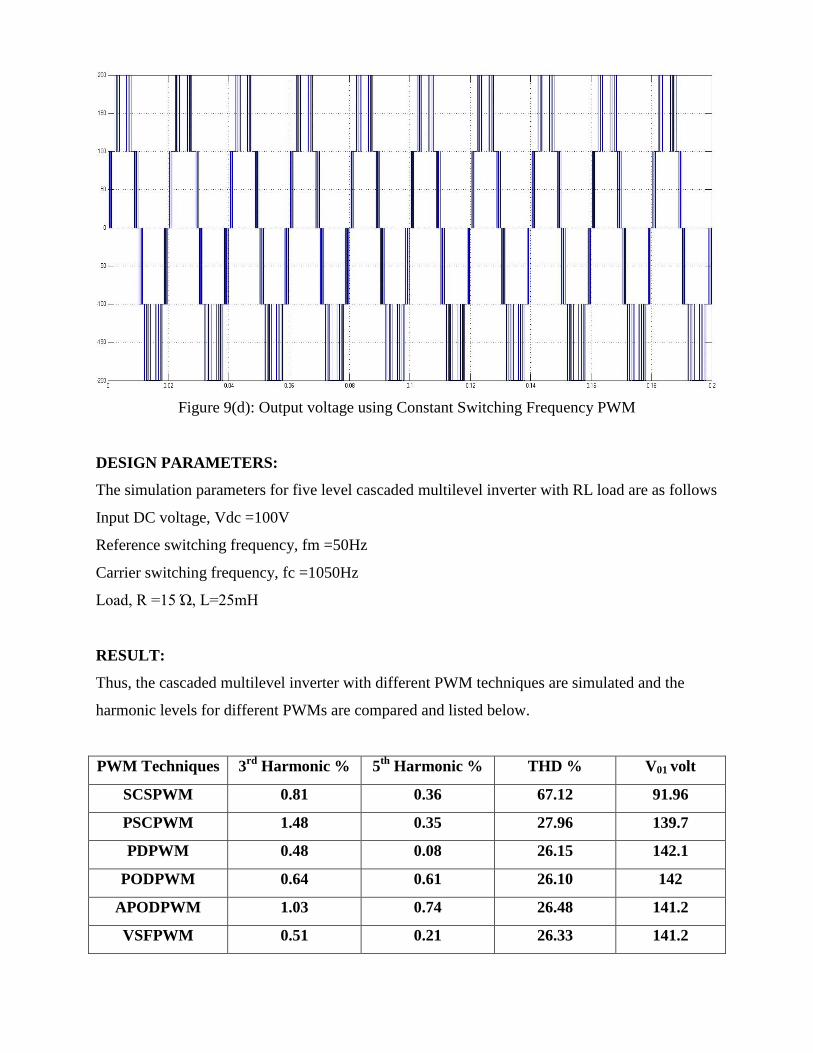
Figure 9(d): Output voltage using Constant Switching Frequency PWM
DESIGN PARAMETERS:
The simulation parameters for five level cascaded multilevel inverter with RL load are as follows
Input DC voltage, Vdc =100V
Reference switching frequency, fm =50Hz
Carrier switching frequency, fc =1050Hz
Load, R =15 Ώ, L=25mH
RESULT:
Thus, the cascaded multilevel inverter with different PWM techniques are simulated and the
harmonic levels for different PWMs are compared and listed below.


![Hybrid Selective Harmonic Elimination PWM for Common ...ijecs.in/issue/v2-i10/22 ijecs.pdf · electroerosion [5]. Different harmonics in Vne can also cause a current to flow through](https://static.documents.pub/doc/80x56/5a83fc277f8b9a24668ed5c5/hybrid-selective-harmonic-elimination-pwm-for-common-ijecsinissuev2-i1022.jpg)


