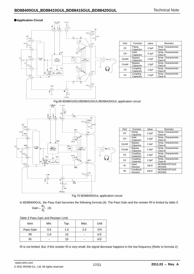
BD88xxxGUL is output coupling capacitorless headphone amplifier. This IC has a negative voltage generator of regulated type built-in and generates the direct regulated negative voltage from the supply voltage. It is possible to drive headphones in a ground standard with both voltage of the positive voltage (+2.4V) and the negative voltage (-2.4V). Therefore a large-capacity output coupling capacitor becomes needless and can reduce a cost, a board area, and the height of the part. In addition, there is not the signal decrement by the low range to happen by output coupling capacitor and output load impedance and can output a rich low tone.
Features 1) 2.4V to 5.5V Single-Supply Operation 2) No Bulky DC-Blocking Capacitors Required 3) No Degradation of Low-Frequency Response Due to Output Capacitors 4) Ground-Referenced Outputs 5) Gain setting BD88400GUL: Variable gain with external resistors BD88410GUL: -1.0V/V BD88415GUL: -1.5V/V BD88420GUL: -2.0V/V 6) Low THD+N 7) Low Supply Current 8) Integrated Negative Power Supply 9) Integrated Short-Circuit and Thermal-Overload Protection 10) Small package VCSP50L2 (2.1mm x 2.1mm)
Applications Mobile Phones, Smart Phones, PDAs, Portable Audio Players, PCs, TVs, Digital Cameras, Digital Video Cameras, Electronic Dictionaries, Voice Recorders, Bluetooth Head-sets, etc
SGND to SHDN_B- voltage VSH (SGND-0.3)~(SVDD+0.3) V
Input current IIN -10~10 mA
Power Dissipation PD 1350 * mW
Storage Temperature Range TSTG -55~150
* In operating over 25 , de-rate the value to 10.8mW/. This value is for mounted on the application board (Grass-epoxy, size: 40mm x 60mm, H=1.6mm, Top Copper area = 79.9%, Bottom Copper area = 80.2%).
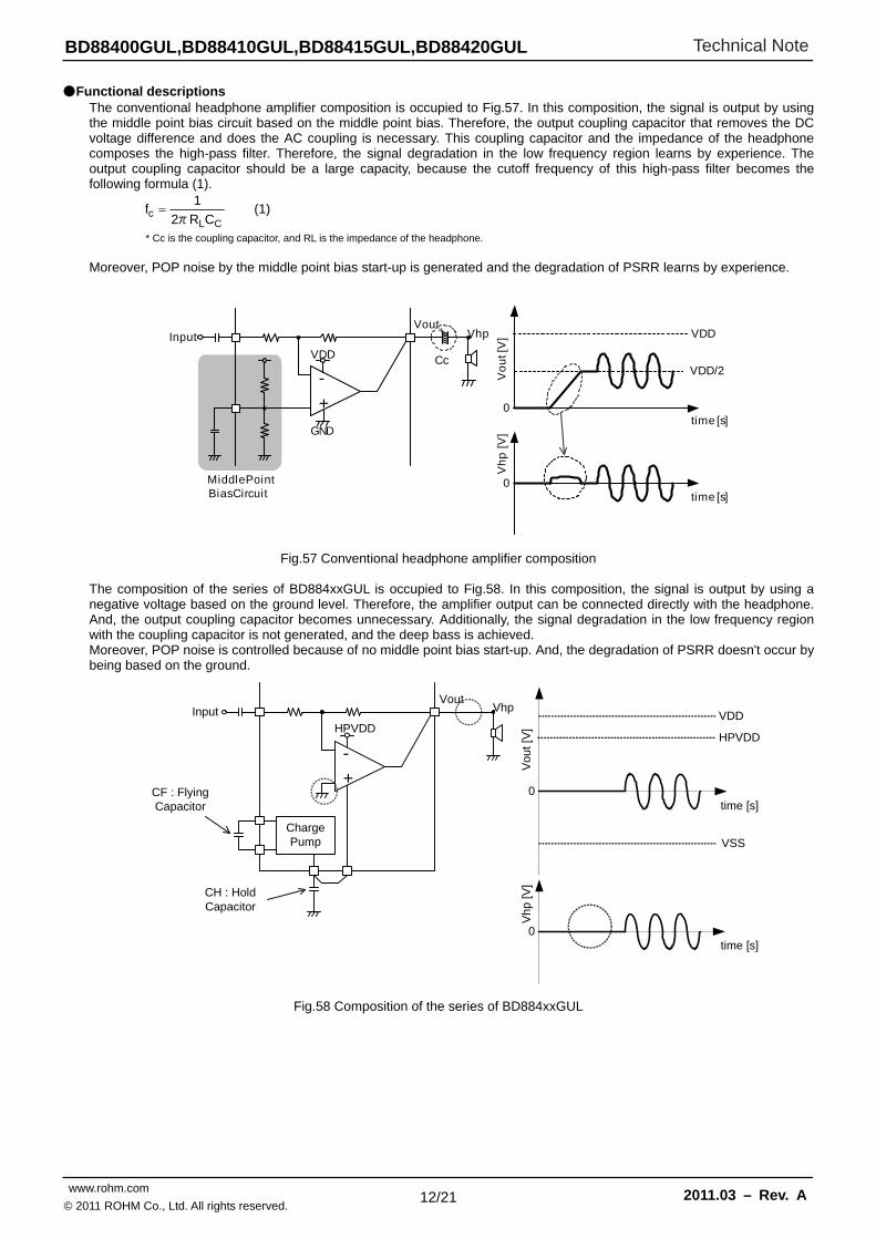
Functional descriptions The conventional headphone amplifier composition is occupied to Fig.57. In this composition, the signal is output by using the middle point bias circuit based on the middle point bias. Therefore, the output coupling capacitor that removes the DC voltage difference and does the AC coupling is necessary. This coupling capacitor and the impedance of the headphone composes the high-pass filter. Therefore, the signal degradation in the low frequency region learns by experience. The output coupling capacitor should be a large capacity, because the cutoff frequency of this high-pass filter becomes the following formula (1).
CLc CR2
1f
π (1)
* Cc is the coupling capacitor, and RL is the impedance of the headphone.
Moreover, POP noise by the middle point bias start-up is generated and the degradation of PSRR learns by experience.
The composition of the series of BD884xxGUL is occupied to Fig.58. In this composition, the signal is output by using a negative voltage based on the ground level. Therefore, the amplifier output can be connected directly with the headphone. And, the output coupling capacitor becomes unnecessary. Additionally, the signal degradation in the low frequency region with the coupling capacitor is not generated, and the deep bass is achieved. Moreover, POP noise is controlled because of no middle point bias start-up. And, the degradation of PSRR doesn't occur by being based on the ground.
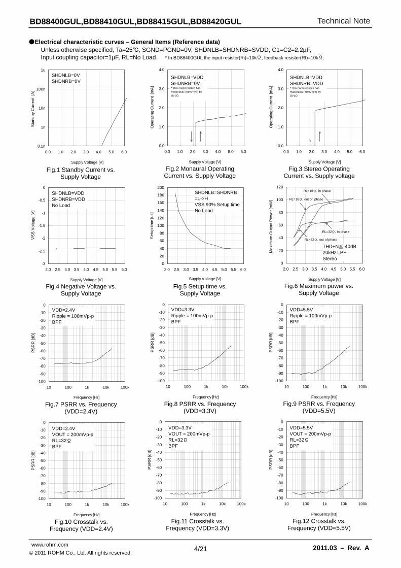
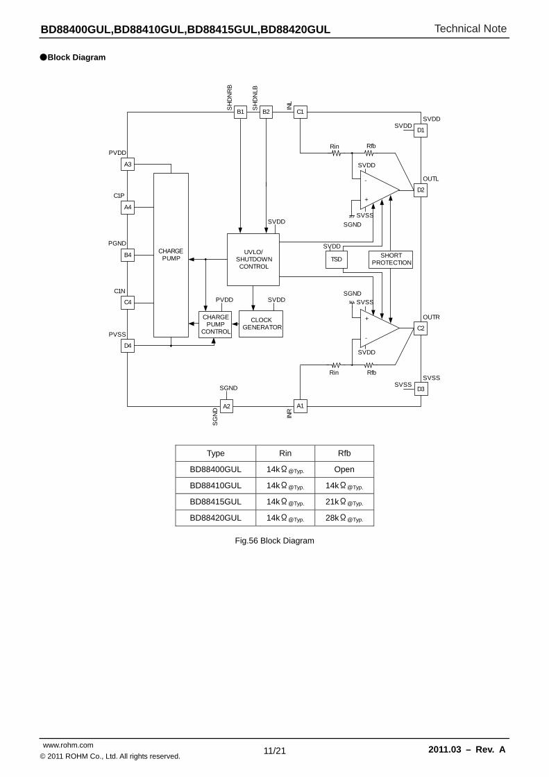
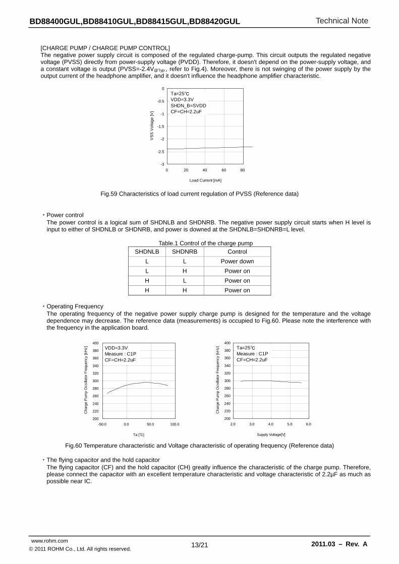
[CHARGE PUMP / CHARGE PUMP CONTROL] The negative power supply circuit is composed of the regulated charge-pump. This circuit outputs the regulated negative voltage (PVSS) directly from power-supply voltage (PVDD). Therefore, it doesn't depend on the power-supply voltage, and a constant voltage is output (PVSS=-2.4V@Typ., refer to Fig.4). Moreover, there is not swinging of the power supply by the output current of the headphone amplifier, and it doesn't influence the headphone amplifier characteristic.
Fig.59 Characteristics of load current regulation of PVSS (Reference data) ・Power control
The power control is a logical sum of SHDNLB and SHDNRB. The negative power supply circuit starts when H level is input to either of SHDNLB or SHDNRB, and power is downed at the SHDNLB=SHDNRB=L level.
Table.1 Control of the charge pump
SHDNLB SHDNRB Control
L L Power down
L H Power on
H L Power on
H H Power on
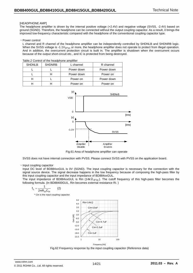
・Operating Frequency
The operating frequency of the negative power supply charge pump is designed for the temperature and the voltage dependence may decrease. The reference data (measurements) is occupied to Fig.60. Please note the interference with the frequency in the application board.
Fig.60 Temperature characteristic and Voltage characteristic of operating frequency (Reference data) ・The flying capacitor and the hold capacitor
The flying capacitor (CF) and the hold capacitor (CH) greatly influence the characteristic of the charge pump. Therefore, please connect the capacitor with an excellent temperature characteristic and voltage characteristic of 2.2µF as much as possible near IC.
[HEADPHONE AMP] The headphone amplifier is driven by the internal positive voltage (+2.4V) and negative voltage (SVSS, -2.4V) based on ground (SGND). Therefore, the headphone can be connected without the output coupling capacitor. As a result, it brings the improved low-frequency characteristic compared with the headphone of the conventional coupling capacitor type. ・Power control
L channel and R channel of the headphone amplifier can be independently controlled by SHDNLB and SHDNRB logic. When the SVSS voltage is -1.1V@Typ. or more, the headphone amplifier does not operate to protect from illegal operation. And in addition, the overcurrent protection circuit is built in. The amplifier is shutdown when the overcurrent occurs because of the output short-circuit etc., and IC is protected from being destroyed.
Table.2 Control of the headphone amplifier
SHDNLB SHDNRB L channel R channel
L L Power down Power down
L H Power down Power on
H L Power on Power down
H H Power on Power on
VDD
0
[V]
[time]
SHDNxB
0
[V]
[time]
SVSS-1.1V
Amplif ierEnable
AmprilierDisable
Fig.61 Area of headphone amplifier can operate
SVSS does not have internal connection with PVSS. Please connect SVSS with PVSS on the application board.
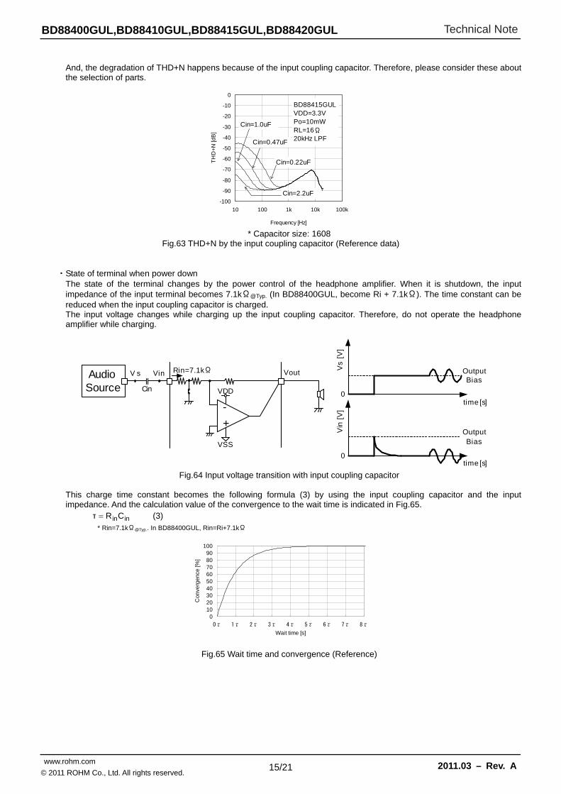
・Input coupling capacitor
Input DC level of BD884xxGUL is 0V (SGND). The input coupling capacitor is necessary for the connection with the signal source device. The signal decrease happens in the low frequency because of composing the high-pass filter by this input coupling capacitor and the input impedance of BD884xxGUL. The input impedance of BD884xxGUL is Rin (14kΩ@Typ.). The cutoff frequency of this high-pass filter becomes the following formula. (In BD88400GUL, Rin becomes external resistance Ri. )
ininc CRπ2
1f (2)
* Cin is the input coupling capacitor.
Fig.62 Frequency response by the input coupling capacitor (Reference data)
And, the degradation of THD+N happens because of the input coupling capacitor. Therefore, please consider these about the selection of parts.
* Capacitor size: 1608 Fig.63 THD+N by the input coupling capacitor (Reference data)
・State of terminal when power down
The state of the terminal changes by the power control of the headphone amplifier. When it is shutdown, the input impedance of the input terminal becomes 7.1kΩ@Typ. (In BD88400GUL, become Ri + 7.1kΩ). The time constant can be reduced when the input coupling capacitor is charged. The input voltage changes while charging up the input coupling capacitor. Therefore, do not operate the headphone amplifier while charging.
AudioSource
+
-
VDD
Vout
time [s]
Vs
[V]
OutputBias
0
VSS
V s Vin
time [s]
Vin
[V
]
OutputBias
0
Cin
Rin =7.1kΩ
Fig.64 Input voltage transition with input coupling capacitor
This charge time constant becomes the following formula (3) by using the input coupling capacitor and the input impedance. And the calculation value of the convergence to the wait time is indicated in Fig.65.
ininCRτ (3) * Rin=7.1kΩ@Typ.. In BD88400GUL, Rin=Ri+7.1kΩ
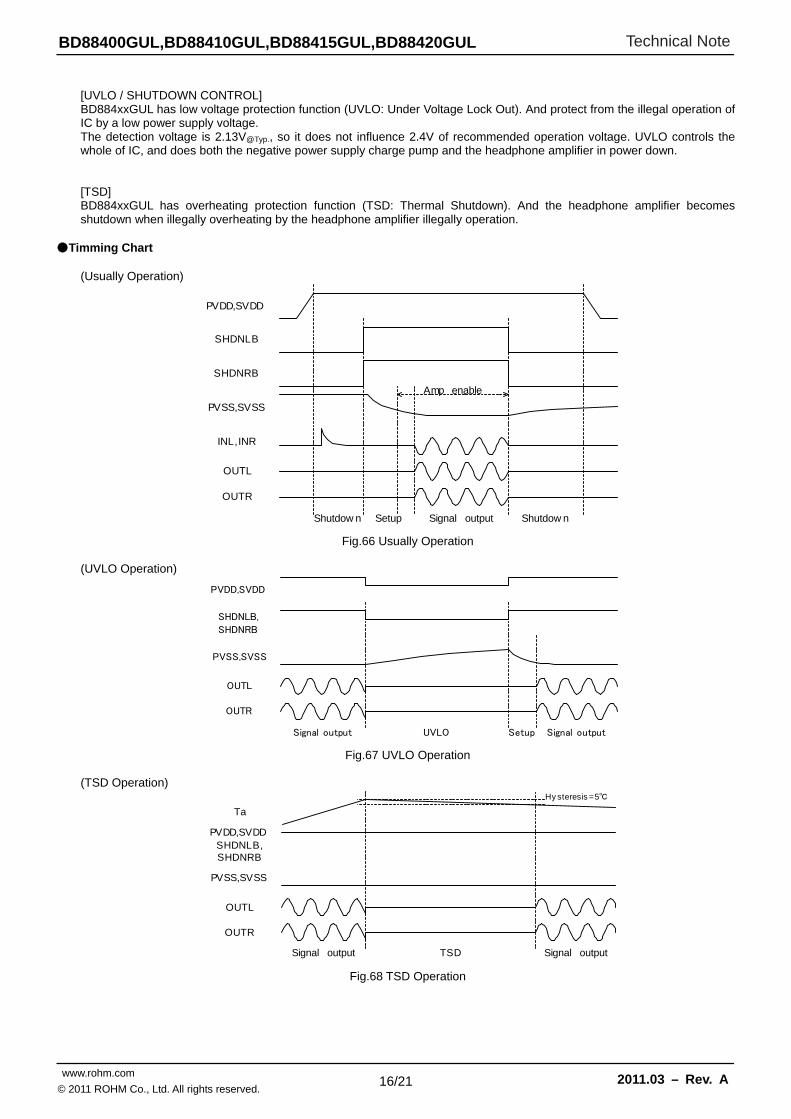
[UVLO / SHUTDOWN CONTROL] BD884xxGUL has low voltage protection function (UVLO: Under Voltage Lock Out). And protect from the illegal operation of IC by a low power supply voltage. The detection voltage is 2.13V@Typ., so it does not influence 2.4V of recommended operation voltage. UVLO controls the whole of IC, and does both the negative power supply charge pump and the headphone amplifier in power down. [TSD] BD884xxGUL has overheating protection function (TSD: Thermal Shutdown). And the headphone amplifier becomes shutdown when illegally overheating by the headphone amplifier illegally operation.
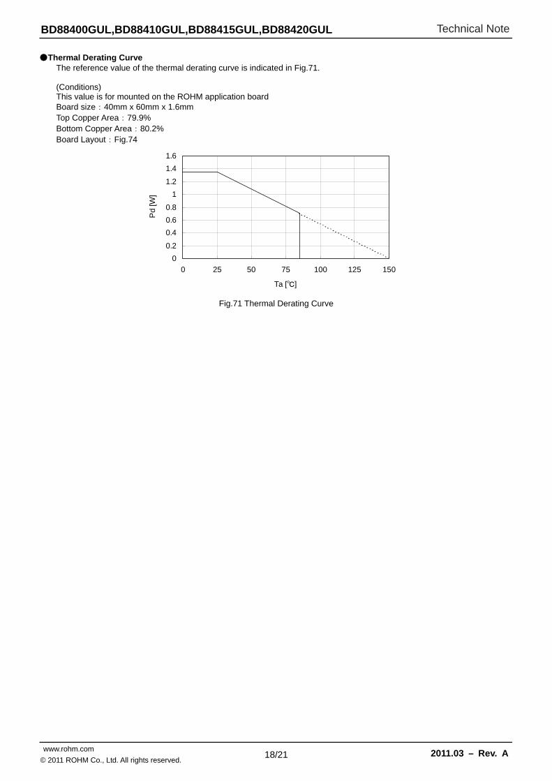
Thermal Derating Curve The reference value of the thermal derating curve is indicated in Fig.71. (Conditions) This value is for mounted on the ROHM application board Board size:40mm x 60mm x 1.6mm Top Copper Area:79.9% Bottom Copper Area:80.2% Board Layout:Fig.74
(1) Absolute Maximum Ratings An excess in the absolute maximum ratings, such as supply voltage, temperature range of operating conditions, etc., can break down devices, thus making impossible to identify breaking mode such as a short circuit or an open circuit. If any special mode exceeding the absolute maximum ratings is assumed, consideration should be given to take physical safety measures including the use of fuses, etc.
(2) Operating conditions These conditions represent a range within which characteristics can be provided approximately as expected. The electrical characteristics are guaranteed under the conditions of each parameter.
(3) Reverse connection of power supply connector The reverse connection of power supply connector can break down ICs. Take protective measures against the breakdown due to the reverse connection, such as mounting an external diode between the power supply and the IC’s power supply terminal.
(4) Power supply line Design PCB pattern to provide low impedance for the wiring between the power supply and the GND lines. In this regard, for the digital block power supply and the analog block power supply, even though these power supplies has the same level of potential, separate the power supply pattern for the digital block from that for the analog block, thus suppressing the diffraction of digital noises to the analog block power supply resulting from impedance common to the wiring patterns. For the GND line, give consideration to design the patterns in a similar manner. Furthermore, for all power supply terminals to ICs, mount a capacitor between the power supply and the GND terminal. At the same time, in order to use an electrolytic capacitor, thoroughly check to be sure the characteristics of the capacitor to be used present no problem including the occurrence of capacity dropout at a low temperature, thus determining the constant.
(5) GND voltage Make setting of the potential of the GND terminal so that it will be maintained at the minimum in any operating state. Furthermore, check to be sure no terminals are at a potential lower than the GND voltage including an actual electric transient.
(6) Short circuit between terminals and erroneous mounting In order to mount ICs on a set PCB, pay thorough attention to the direction and offset of the ICs. Erroneous mounting can break down the ICs. Furthermore, if a short circuit occurs due to foreign matters entering between terminals or between the terminal and the power supply or the GND terminal, the ICs can break down.
(7) Operation in strong electromagnetic field Be noted that using ICs in the strong electromagnetic field can malfunction them.
(8) Inspection with set PCB On the inspection with the set PCB, if a capacitor is connected to a low-impedance IC terminal, the IC can suffer stress. Therefore, be sure to discharge from the set PCB by each process. Furthermore, in order to mount or dismount the set PCB to/from the jig for the inspection process, be sure to turn OFF the power supply and then mount the set PCB to the jig. After the completion of the inspection, be sure to turn OFF the power supply and then dismount it from the jig. In addition, for protection against static electricity, establish a ground for the assembly process and pay thorough attention to the transportation and the storage of the set PCB.
(9) Input terminals In terms of the construction of IC, parasitic elements are inevitably formed in relation to potential. The operation of the parasitic element can cause interference with circuit operation, thus resulting in a malfunction and then breakdown of the input terminal. Therefore, pay thorough attention not to handle the input terminals, such as to apply to the input terminals a voltage lower than the GND respectively, so that any parasitic element will operate. Furthermore, do not apply a voltage to the input terminals when no power supply voltage is applied to the IC. In addition, even if the power supply voltage is applied, apply to the input terminals a voltage lower than the power supply voltage or within the guaranteed value of electrical characteristics.
(10) Ground wiring pattern If small-signal GND and large-current GND are provided, It will be recommended to separate the large-current GND pattern from the small-signal GND pattern and establish a single ground at the reference point of the set PCB so that resistance to the wiring pattern and voltage fluctuations due to a large current will cause no fluctuations in voltages of the small-signal GND. Pay attention not to cause fluctuations in the GND wiring pattern of external parts as well.
(11) External capacitor In order to use a ceramic capacitor as the external capacitor, determine the constant with consideration given to a degradation in the nominal capacitance due to DC bias and changes in the capacitance due to temperature, etc.
(12) About the rush current For ICs with more than one power supply, it is possible that rush current may flow instantaneously due to the internal powering sequence and delays. Therefore, give special consideration to power coupling capacitance, power wiring, width of GND wiring, and routing of wiring.
1. Our Products are designed and manufactured for application in ordinary electronic equipments (such as AV equipment, OA equipment, telecommunication equipment, home electronic appliances, amusement equipment, etc.). If you intend to use our Products in devices requiring extremely high reliability (such as medical equipment (Note 1), transport equipment, traffic equipment, aircraft/spacecraft, nuclear power controllers, fuel controllers, car equipment including car accessories, safety devices, etc.) and whose malfunction or failure may cause loss of human life, bodily injury or serious damage to property (“Specific Applications”), please consult with the ROHM sales representative in advance. Unless otherwise agreed in writing by ROHM in advance, ROHM shall not be in any way responsible or liable for any damages, expenses or losses incurred by you or third parties arising from the use of any ROHM’s Products for Specific Applications.
(Note1) Medical Equipment Classification of the Specific Applications JAPAN USA EU CHINA
CLASSⅢ CLASSⅢ
CLASSⅡb CLASSⅢ
CLASSⅣ CLASSⅢ
2. ROHM designs and manufactures its Products subject to strict quality control system. However, semiconductor
products can fail or malfunction at a certain rate. Please be sure to implement, at your own responsibilities, adequate safety measures including but not limited to fail-safe design against the physical injury, damage to any property, which a failure or malfunction of our Products may cause. The following are examples of safety measures:
[a] Installation of protection circuits or other protective devices to improve system safety [b] Installation of redundant circuits to reduce the impact of single or multiple circuit failure
3. Our Products are designed and manufactured for use under standard conditions and not under any special or extraordinary environments or conditions, as exemplified below. Accordingly, ROHM shall not be in any way responsible or liable for any damages, expenses or losses arising from the use of any ROHM’s Products under any special or extraordinary environments or conditions. If you intend to use our Products under any special or extraordinary environments or conditions (as exemplified below), your independent verification and confirmation of product performance, reliability, etc, prior to use, must be necessary:
[a] Use of our Products in any types of liquid, including water, oils, chemicals, and organic solvents [b] Use of our Products outdoors or in places where the Products are exposed to direct sunlight or dust [c] Use of our Products in places where the Products are exposed to sea wind or corrosive gases, including Cl2,
H2S, NH3, SO2, and NO2
[d] Use of our Products in places where the Products are exposed to static electricity or electromagnetic waves [e] Use of our Products in proximity to heat-producing components, plastic cords, or other flammable items [f] Sealing or coating our Products with resin or other coating materials [g] Use of our Products without cleaning residue of flux (even if you use no-clean type fluxes, cleaning residue of
flux is recommended); or Washing our Products by using water or water-soluble cleaning agents for cleaning residue after soldering
[h] Use of the Products in places subject to dew condensation
4. The Products are not subject to radiation-proof design. 5. Please verify and confirm characteristics of the final or mounted products in using the Products. 6. In particular, if a transient load (a large amount of load applied in a short period of time, such as pulse. is applied,
confirmation of performance characteristics after on-board mounting is strongly recommended. Avoid applying power exceeding normal rated power; exceeding the power rating under steady-state loading condition may negatively affect product performance and reliability.
7. De-rate Power Dissipation (Pd) depending on Ambient temperature (Ta). When used in sealed area, confirm the actual
ambient temperature. 8. Confirm that operation temperature is within the specified range described in the product specification. 9. ROHM shall not be in any way responsible or liable for failure induced under deviant condition from what is defined in
this document.
Precaution for Mounting / Circuit board design 1. When a highly active halogenous (chlorine, bromine, etc.) flux is used, the residue of flux may negatively affect product
performance and reliability. 2. In principle, the reflow soldering method must be used; if flow soldering method is preferred, please consult with the
ROHM representative in advance. For details, please refer to ROHM Mounting specification
Precautions Regarding Application Examples and External Circuits 1. If change is made to the constant of an external circuit, please allow a sufficient margin considering variations of the
characteristics of the Products and external components, including transient characteristics, as well as static characteristics.
2. You agree that application notes, reference designs, and associated data and information contained in this document
are presented only as guidance for Products use. Therefore, in case you use such information, you are solely responsible for it and you must exercise your own independent verification and judgment in the use of such information contained in this document. ROHM shall not be in any way responsible or liable for any damages, expenses or losses incurred by you or third parties arising from the use of such information.
Precaution for Electrostatic
This Product is electrostatic sensitive product, which may be damaged due to electrostatic discharge. Please take proper caution in your manufacturing process and storage so that voltage exceeding the Products maximum rating will not be applied to Products. Please take special care under dry condition (e.g. Grounding of human body / equipment / solder iron, isolation from charged objects, setting of Ionizer, friction prevention and temperature / humidity control).
Precaution for Storage / Transportation 1. Product performance and soldered connections may deteriorate if the Products are stored in the places where:
[a] the Products are exposed to sea winds or corrosive gases, including Cl2, H2S, NH3, SO2, and NO2 [b] the temperature or humidity exceeds those recommended by ROHM [c] the Products are exposed to direct sunshine or condensation [d] the Products are exposed to high Electrostatic
2. Even under ROHM recommended storage condition, solderability of products out of recommended storage time period may be degraded. It is strongly recommended to confirm solderability before using Products of which storage time is exceeding the recommended storage time period.
3. Store / transport cartons in the correct direction, which is indicated on a carton with a symbol. Otherwise bent leads
may occur due to excessive stress applied when dropping of a carton. 4. Use Products within the specified time after opening a humidity barrier bag. Baking is required before using Products of
which storage time is exceeding the recommended storage time period.
Precaution for Product Label QR code printed on ROHM Products label is for ROHM’s internal use only.
Precaution for Disposition When disposing Products please dispose them properly using an authorized industry waste company.
Precaution for Foreign Exchange and Foreign Trade act Since our Products might fall under controlled goods prescribed by the applicable foreign exchange and foreign trade act, please consult with ROHM representative in case of export.
Precaution Regarding Intellectual Property Rights 1. All information and data including but not limited to application example contained in this document is for reference
only. ROHM does not warrant that foregoing information or data will not infringe any intellectual property rights or any other rights of any third party regarding such information or data. ROHM shall not be in any way responsible or liable for infringement of any intellectual property rights or other damages arising from use of such information or data.:
2. No license, expressly or implied, is granted hereby under any intellectual property rights or other rights of ROHM or any
third parties with respect to the information contained in this document.
Other Precaution 1. This document may not be reprinted or reproduced, in whole or in part, without prior written consent of ROHM. 2. The Products may not be disassembled, converted, modified, reproduced or otherwise changed without prior written
consent of ROHM. 3. In no event shall you use in any way whatsoever the Products and the related technical information contained in the
Products or this document for any military purposes, including but not limited to, the development of mass-destruction weapons.
4. The proper names of companies or products described in this document are trademarks or registered trademarks of
General Precaution 1. Before you use our Pro ducts, you are requested to care fully read this document and fully understand its contents.
ROHM shall n ot be in an y way responsible or liabl e for fa ilure, malfunction or acci dent arising from the use of a ny ROHM’s Products against warning, caution or note contained in this document.
2. All information contained in this docume nt is current as of the issuing date and subj ect to change without any prior
notice. Before purchasing or using ROHM’s Products, please confirm the la test information with a ROHM sale s representative.
3. The information contained in this doc ument is provi ded on an “as is” basis and ROHM does not warrant that all
information contained in this document is accurate an d/or error-free. ROHM shall not be in an y way responsible or liable for any damages, expenses or losses incurred by you or third parties resulting from inaccuracy or errors of or concerning such information.