SANDIA REPORT SAND2006-2209 Unlimited Release Printed April 2006 Hemispheric Ultra-Wideband Antenna Robert W. Brocato Prepared by Sandia National Laboratories Albuquerque, New Mexico 87185 and Livermore, California 94550 Sandia is a multiprogram laboratory operated by Sandia Corporation, A Lockheed Martin Company, for the United States Department of Energy’s National Nuclear Security Administration under Contract DE-AC04-94AL85000. Approved for public release; further dissemination unlimited.
Transcript
SANDIA REPORT SAND2006-2209 Unlimited Release Printed April 2006
Hemispheric Ultra-Wideband Antenna Robert W. Brocato Prepared by Sandia National Laboratories Albuquerque, New Mexico 87185 and Livermore, California 94550 Sandia is a multiprogram laboratory operated by Sandia Corporation, A Lockheed Martin Company, for the United States Department of Energy’s National Nuclear Security Administration under Contract DE-AC04-94AL85000.
Approved for public release; further dissemination unlimited.
Issued by Sandia National Laboratories, operated for the United States Department of Energy by Sandia Corporation. NOTICE: This report was prepared as an account of work sponsored by an agency of the United States Government. Neither the United States Government nor any agency thereof, nor any of their employees, nor any of their contractors, subcontractors, or their employees, makes any warranty, express or implied, or assumes any legal liability or responsibility for the accuracy, completeness, or usefulness of any information, apparatus, product, or process disclosed, or represents that its use would not infringe privately owned rights. Reference herein to any specific commercial product, process, or service by trade name, trademark, manufacturer, or otherwise, does not necessarily constitute or imply its endorsement, recommendation, or favoring by the United States Government, any agency thereof or any of their contractors or subcontractors. The views and opinions expressed herein do not necessarily state or reflect those of the United States Government, any agency thereof or any of their contractors or subcontractors. Printed in the United States of America. This report has been reproduced directly from the best available copy. Available to DOE and DOE contractors from U.S. Department of Energy Office of Scientific and Technical Information P.O. Box 62 Oak Ridge, TN 37831 Telephone: (865) 576-8401 Facsimile: (865) 576-5728 E-mail: [email protected] Online ordering: http://www.doe.gov/bridge Available to the public from U.S. Department of Commerce National Technical Information Service 5285 Port Royal Rd. Springfield, VA 22161 Telephone: (800) 553-6847 Facsimile: (703) 605-6900 E-Mail: [email protected] Online ordering: http://www.ntis.gov/ordering.htm
SAND2006-2209 Unlimited Release Printed April 2006
Hemispheric Ultra-Wideband Antenna
Robert W. Brocato Sandia National Laboratories Opto and RF Microsystems
P.O. Box 5800 Albuquerque, NM 87185
Abstract: This report begins with a review of reduced size ultra-wideband (UWB) antennas and the peculiar problems that arise when building a UWB antenna. It then gives a description of a new type of UWB antenna that resolves these problems. This antenna, dubbed the hemispheric conical antenna, is similar to a conventional conical antenna in that it uses the same inverted conical conductor over a ground plane, but it also uses a hemispheric dielectric fill in between the conductive cone and the ground plane. The dielectric material creates a fundamentally new antenna which is reduced in size and much more rugged than a standard UWB conical antenna.. The creation of finite-difference time domain (FDTD) software tools in spherical coordinates, as described in SAND2004-6577, enabled this technological advance.
3
This page is left intentionally blank.
4
Contents Section .......................................................................................................Page Abstract ........................................................................................................... 3 Nomenclature.................................................................................................. 6 Introduction..................................................................................................... 7 Background ..................................................................................................... 7 Current Physically Constrained UWB Antennas............................................ 9 Physically Constrained UWB Cone Antenna: Overview............................. 10 Electric and Magnetic Field Derivation........................................................ 11 Radiation Density and Intensity.................................................................... 15 Conical Antenna with Dielectric Over an Infinite Ground Plane................. 14 Simulations ................................................................................................... 18 Antenna Input Impedance............................................................................. 19 Simulation Results: Unmatched Antenna..................................................... 21 Simulation Results: Matched Antenna ......................................................... 25 Conclusion .................................................................................................... 27 References..................................................................................................... 27 Distribution ................................................................................................... 29
5
Nomenclature
B - Magnetic flux density vector D - Electric flux density vector E - Electric field intensity vector FDTD - Finite Difference Time Domain analysis FY - Fiscal Year GHz - Giga Hertz (billion cycles/sec) H - Magnetic field intensity vector HFSS - Three dimensional electro-magnetic field simulator Je - Electric current density Jm - Magnetic current density LTCC - Low Temperature Co-fired Ceramic MATLAB - Simulation software available from MathWorks MathCAD - Simulation software available from MathSoft MCCA - Multilayer Ceramic Chip Antenna MHz - Mega Hertz (million cycles/sec) MOM - Method of Moments simulator NIST - National Institute of Standards PCB - Printed Circuit Board PIFA - Planar Inverted F Antenna PML - Perfectly Matched Layer TEM - Transverse Electro-Magnetic wave UWB - Ultra-WideBand VSWR - Voltage Standing Wave Ratio
6
Introduction Reducing antenna size is a ongoing effort for a large and growing number of applications. As electronic communications become more ubiquitous, it is increasingly important that those electronic devices become smaller. The antenna is often left as the sole component resisting significant size reductions. A great deal of attention is being given to reducing antenna size, especially for mobile communications. This work starts by briefly reviewing recent efforts to reduce antenna size for mobile communication applications. It then moves on to examine some specific efforts at building reduced size antennas for ultra-wideband (UWB) applications. The special problems of building UWB antennas are examined, including the extreme sensitivity of such antennas to impedance mismatches. Then, a physically constrained, reduced size antenna for UWB applications is introduced. This antenna is a variant of a conical horn antenna and consists of an inverted cone positioned over a ground plane and surrounded by a hemisphere of dielectric material. This antenna will henceforth be referred to as a hemispheric conical antenna, to distinguish it from the conventional conical antenna. The remainder of the paper examines the properties of this antenna, including a derivation of closed form equations for far field electric and magnetic field vectors, radiation intensity, and directivity. Some variants of the antenna are investigated, and an optimized antenna geometry, with properties superior to those of standard UWB antennas, is discussed. Time domain properties of optimized and unoptimized versions are examined when propagating UWB Gaussian pulses. This analysis demonstrates the critical importance of time domain analysis in the investigation of UWB components. Background There is currently a growing interest in very small communication devices. Some project that by the year 2013, chip-to-chip communications will be dominant at frequencies as high as 90 and 170GHz [1]. They point out that a λ/2 dipole on silicon at 90GHz is only 480μm long, indicating that on-chip antennas will become more common as frequencies move up. Since silicon is a lossy substrate material, these antennas may need to be fabricated using techniques being developed now, with more conventional materials. Many examples of small and reduced size antennas are already used extensively in commercial products. Loaded dipole, meander patch, planar inverted-F (PIFA), and quadrifilar helical antennas are all examples of popular configurations used to reduce antenna size [2] [3] [4]. These antennas are typically not well suited to very wideband or UWB applications, and so they may need to be modified or replaced by a new group of antennas suitable for these newer communication methodologies. Design of reduced size antennas is difficult and requires extensive use of simulation tools. Method-of-moments (MOM) type simulators such as HFSS appear to be the most popular tools in the investigation of chip-type antennas [5]. Most of these popular simulators operate in rectangular, or Cartesian, coordinates, and, not surprisingly, the antennas that are successfully designed with them tend to be rectangular. As will be shown, this may be leading investigators to overlook some very useful antenna
3
geometries. Similarly, the use of MOM simulators may be leading investigators to neglect examining and optimizing the critical time domain performance of wideband and UWB antennas. Use of MOM simulators for designing compact antennas is leading to a large number of new designs of multilayer ceramic chip antennas (MCCA). Low-temperature co-fired ceramic (LTCC) and other electronics packaging technologies are used to fabricate MCCA’s [6]. These are popular for mobile communications in the cellular and Part-15 bands not only for their small size, but also for their physical ruggedness and manufacturability. The term manufacturability generally implies low cost. These three requirements, small size, ruggedness, and low cost, are the main points that determine the acceptance of an antenna into the mobile communications marketplace. There are four general categories into which reduced size antennas can be subdivided. These are as follows [7]:
1) Electrically small antennas are those antennas that will fit within a sphere with a radius less than λ/2π.
2) Physically constrained antennas are not quite electrically small, but still achieve considerable size reduction in at least one plane.
3) Functionally small antennas are not necessarily reduced in size but have improved performance that is achieved without an increase in size.
4) Physically small antennas may not fit into any of the above three categories, yet their dimensions are small in some relative sense.
There is some dispute over the definition of the sphere radius, or Wheeler radiansphere, into which an electrically small antenna must fit. Some accept the definition given above, some require it to be as small as λ/30 [8]. Size reductions for UWB antennas generally do not quite meet either requirement. One significant example of an electrically small antenna is the spherical dipole antenna [9]. This antenna fits a self-resonant dipole antenna with a 50Ω input impedance into a spherical shape with a diameter less than λ/23. It achieves an efficiency in excess of 95% by shaping the dipole wires into a spherical helix shape. The antenna exhibits an omni-directional radiation pattern but achieves all of these significant advantages at the expense of narrow bandwidth. The antenna Q of a spherical dipole antenna is reported to be in excess of 87. UWB applications require a Q of less than 2. Regardless of the accepted definition of an electrically small antenna, the antenna investigated henceforth in this work is really only physically constrained, fitting into category (2) above. It is reduced in size in the “r” dimension but not with enough reduction to satisfy even the relaxed definition of an electrically small antenna. Electrically small antennas encounter significant bandwidth limitations [10], and it will be shown that these bandwidth limitations begin to unacceptably impact UWB antennas in their time domain responses.
4
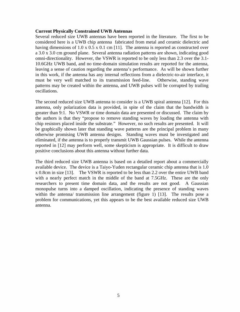
Current Physically Constrained UWB Antennas Several reduced size UWB antennas have been reported in the literature. The first to be considered here is a UWB chip antenna fabricated from metal and ceramic dielectric and having dimensions of 1.0 x 0.5 x 0.1 cm [11]. The antenna is reported as constructed over a 3.0 x 3.0 cm ground plane. Several antenna radiation patterns are shown, indicating good omni-directionality. However, the VSWR is reported to be only less than 2.3 over the 3.1-10.6GHz UWB band, and no time-domain simulation results are reported for the antenna, leaving a sense of caution regarding the antenna’s performance. As will be shown further in this work, if the antenna has any internal reflections from a dielectric-to-air interface, it must be very well matched to its transmission feed-line. Otherwise, standing wave patterns may be created within the antenna, and UWB pulses will be corrupted by trailing oscillations. The second reduced size UWB antenna to consider is a UWB spiral antenna [12]. For this antenna, only polarization data is provided, in spite of the claim that the bandwidth is greater than 9:1. No VSWR or time domain data are presented or discussed. The claim by the authors is that they “propose to remove standing waves by loading the antenna with chip resistors placed inside the substrate.” However, no such results are presented. It will be graphically shown later that standing wave patterns are the principal problem in many otherwise promising UWB antenna designs. Standing waves must be investigated and eliminated, if the antenna is to properly transmit UWB Gaussian pulses. While the antenna reported in [12] may perform well, some skepticism is appropriate. It is difficult to draw positive conclusions about this antenna without further data. The third reduced size UWB antenna is based on a detailed report about a commercially available device. The device is a Taiyo-Yuden rectangular ceramic chip antenna that is 1.0 x 0.8cm in size [13]. The VSWR is reported to be less than 2.2 over the entire UWB band with a nearly perfect match in the middle of the band at 7.5GHz. These are the only researchers to present time domain data, and the results are not good. A Gaussian monopulse turns into a damped oscillation, indicating the presence of standing waves within the antenna/ transmission line arrangement (figure 1) [13]. The results pose a problem for communications, yet this appears to be the best available reduced size UWB antenna.
5
hysically Constrained UWB Cone Antenna: Overview everal main points have been established thus far. First, it is advantageous to reduce ntenna size for mobile applications. Second, making a UWB antenna electrically small ay be an unrealistic goal due to accompanying bandwidth reductions. Finally, UWB
ntennas are extremely sensitive to impedance matching and, therefore, internal standing aves. For Gaussian pulse-based UWB communications, these standing waves can verely limit pulse detection.
ne additional point should be made regarding deploying practical UWB antennas. That oint is that the UWB antenna should be physically robust. The subject of making ntennas physically robust and resistant to breakage is an important one, and there are ntire papers dedicated solely to the subject of making an antenna stronger without
pacting its electrical properties [14]. In the case of UWB antennas, the transmit and ceive antennas recommended by the National Bureau of Standards (NIST) are the conical
ntenna and the transverse electromagnetic (TEM) horn antenna [15]. Both of these ntennas contain no dielectric, do not have surrounding radomes, and are physically fragile
ically robust is to add dielectric
nalysis of the conical antenna without any dielectric fill was
PSamawse Opaeimreaa[16]. The logical solution to make the conical antenna physin a hemispheric shape between the metal cone and the ground plane (figure 2). The remainder of this report will cover the design details to settle on the optimum semi-angle of the cone and the dielectric constant of the hemispheric fill. The analysis makes use of the finite difference time-domain (FDTD) technique in spherical coordinates using equations derived from first principles and correlating in most respects
ith those described in [17]. Awpreviously conducted by the author and [18]. Analysis of the hemispheric (dielectric filled) conical antenna has not been reported in the literature, so apparently, the analysis presented in this report is new.
6
Electric
ntenna and then using symmetry for the conical case. For this analysis, consider that the round plane and dielectric are removed from figure 1. The conical antenna is then xtended to infinity, replicated, and flipped 180o to form an infinite, bi-conical antenna.
To start the analysis, the field equations in E and H can now be derived. To ccomplish this, we can first start with two of Maxwell’s equations and the medium ependent equations, as follows:
)
and Magnetic Field Derivation The conical antenna can be analyzed in closed form by considering a bi-conical
age
ad
t
BJE m ∂
∂−−=×∇
vv
1
t
DJH e ∂
∂+=×∇
vv
2)
34
) B = μ H ) D = ε E
5) Je = σ E 6) Jm = σ* M
Combining these, one obtains two vector versions of Maxwell’s equations:
7) t
HHE
δδμσv
vv⋅−⋅−=×∇ *
7
t
EEH
δδεσv
vv⋅+⋅=×∇8)
These two vector equations are the general equations governing the antenna operation. can only be effectively analyzed in spherical coordinates. This will involve
thematics initially but will enable the analysis and simulation of the ordinate boundaries. To get started, the two
e expanded using the spherical ∇ operator:
This antenna some complicated maantenna with transitions only along spherical covector equations must b
The vector equations (13) and (15) produce six scalar Maxwell’s equations from equating the r, θ, and φ vector terms each into a separate scalar equation: 16) δH /δt = 1/μ (δE /(r sinθ δφ) – 1/ (sinθ) δ/(r δθ) (sinθ )) + (σ*/μ) H
δ(r δθ) (sinθ Er) – 1/r δ/δr (r Eθ)) + (σ*/μ) Hφ
δt = 1/ δθ /(r sinθ δφ)) – (σ / ε) Er
+⋅=∇ rr
θ, and φ being the spherical unit vectors. The ∇ operator is first applied to
∇ x E =
r θ φ
E E E
These two cross products each produce vector equations that are another way of writing equations 10 and 11: 12) -μ δH/δt = σ*H + ∇ x E or, expanding… 13) -μ δH/δt = 1/(r sinθ) ((δ/δθ (sinθ Eφ) - δEθ/δφ) r + (δE
21) δE /δt = 1/ε (1/r δ/δr (r H ) – 1/(sinθ )δ/(r δθ) (sinθ H )) – ( / ε) Eφ θ r σ
φ
r θ φ
∇ x H =
r θ φand
11)
Hr Hθ Hφ
10) ⋅⋅ θsin
1r
⋅⋅ θsin
1r
( )θsin⋅∂∂
rr
( )θsin⋅∂∂
rr
( )θθ
sin∂∂
( )θθ
sin∂∂
φ∂∂
φ∂∂
8
These (16-21) are the general three dimensional equations that describe electromagnetic t we can use to obtain closed
rm approximations for E and H is symmetrical about φ and can be analyzed in two dimens
and σ*, are zero the propagation space for a closed form analysis. These terms are not zero in free space
uities into the
is not zero at the , since all field components
ad one to conclude e a ponents in φ must be
es with –jωt,
s defined by the FCC The simplified partial differential equations in (22)-(24) are coupled and must also y the boundary constraints of the bi-conical antenna. One can readily
bserve that (22) and (24) imply spherical wave solutions with a spatial variation of exp(-or an outwardly travelin r)/r for an inwardly traveling wave. It is pparent the a time variation of exp(jωt)/r must be in the solution. Applying (23) at
e edge of the cone of semi-angle θo gives:
waves in spherical coordinates. The bi-conical antenna thafo
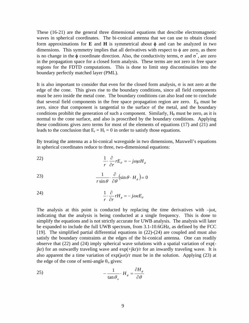
ions. This symmetry implies that all derivatives with respect to φ are zero, as there is no change in the φ coordinate direction. Also, the conductivity terms, σinregions for the FDTD computations. This is done to limit step discontinboundary perfectly matched layer (PML). It is also important to consider that even for the closed form analysis, σedge of the cone. This gives rise to the boundary conditionsmust be zero inside the metal cone. The boundary conditions can also le
at s ver l field com the free space propagation region are zero. Ethzero, since that component is tangential to the surface of the metal, and the boundary conditions prohibit the generation of such a component. Similarly, Hθ must be zero, as it is normal to the cone surface, and also is proscribed by the boundary conditions. Applying these conditions gives zero terms for most of the elements of equations (17) and (21) and leads to the conclusion that Er = Hr = 0 in order to satisfy those equations. By treating the antenna as a bi-conical waveguide in two dimensions, Maxwell’s equations in spherical coordinates reduce to three, two-dimensional equations: 22) 23) 24)
he analysis at this point is conducted by replacing the time derivativ
φθ ωμHjrErr
−=∂∂
⋅1
( ) 0sinsin1
=⋅∂∂
⋅ φθθθ
Hr
θφ ωεEjrHrr
−=∂∂
⋅1
Tindicating that the analysis is being conducted at a single frequency. This is done to simplify the equations and is not strictly accurate for UWB analysis. The analysis will later e expanded to include the full UWB spectrum, from 3.1-10.6GHz, ab
[19]. atisfs
o at the edges
jkr) flso a
g wave and exp(+jkath 5)
θθφ
φ ∂
∂=⋅−
HH
otan12
9
This implies a solution that includes a multiplier of 1/(sinθ) to satisfy the boundary condition. Using this information, the following solutions can be constructed, and substitution into (22)-(24) will verify their validity: 26) 27)
[ ]))(exp())(exp(sin
krtjBkrtjAr
E ++−⋅= ωωθ
ηθ
[ ]))(exp())(exp(sin1
krtjBkrtjAr
H ++−⋅= ωωθφ
Additionally, as has been already deduced, the other field components must be zero:
8)
eling waves.
t this point one can so with currents either re related to the magnetic field. A relation between the azimuthal magnetic field and
e corresponding current in the cones can be calculated from the magnetic curl relation:
nθ. ne can replace the coefficients, A and B, with currents, IA and IB, in accordance with
on (29). That is, A or constants governed by the lations:
1)
ons in (28), (31), and (32) are for an infinite bi-conical antenna at a single equency. It will be shown in the simulation results that these solutions are also
imately correct as far-field solutions to a small conical antenna over a ground plane.
2 The two dimensional wave solutions in (26)-(28) are the same as those presented in [20]. They include terms for both inward and outward trav
0= = = =θφ rr HHEE
A lve to eliminate the constants and replace themthat ath
θπ φ sin2 HrldHIC
⋅⋅=⋅= ∫vv29)
Since the curve C is a circumference of the cone at a radius of r, then C = 2πa = 2πr siOrelati and B are magnetic field vectre 30) The field equations can now be expressed in terms of the currents in the cones: 3 32) The solutifrapprox
π2AI
A =π2BI
B =
[ ]))(exp())(exp(sin2
krtjIkrtjIr
E ++−⋅⋅
= ωωπ BAθ
ηθ
[ ]))(exp())(exp(1krtjIkrtjI
sin2 rH ++−⋅= ωω BA⋅ θπφ
10
Radiation Density and Intensity e must first
onsider the instantaneous Poynting vector for the antenna in the transmit mode. In this the inwardly traveling wave is taken to be zero (i.e. IB = B = 0) and the Poynting
ector, or instantaneous radiation density, is found from the outwardly traveling wave:
3)
4)
ty is From the radiation density, one
6)
L igure 3) included in the software with reference [21]. The equation is plotted for an ntenna with a semi
he total radiated power can also be found from the average radiation density by tegrating over the free space propagation region:
8)
olving the definite integral:
rHEHxEWrad
In order to further analyze the radiative properties of the bi-conical antenna, onccase, v v v v v3 φθ== 3 Taking the time average of the Poynting vector gives the time average radiation density:
rkrtjI
W Arad
vv⋅⎥
⎤⎢⎡ −⋅=
2
))(exp( ωηr ⎦⎣ ⋅ sin2 θπ
35) It should be noted that the radiation density given by (35) is valid only in the free space egions of the solution space. In the metal portions of the antenna, the radiation densi
2⎤⎡η Ivv
sin22)Re(
2 ⎥⎦⎢⎣ ⋅⋅=⋅=
θπ rHxEW A
avg
1v
rzero.
can obtain the radiation intensity:
32⎤⎡η I2
sin8 ⎥⎦⎢⎣ ⋅⋅=⋅=
θπA
avgWrU The radiation intensity pattern from (36) is plotted using the Matlab routine SPHERICA(fa -angle of 30o and without any dielectric. Tin 37)
∫∫ ∂•=S
avgrad SWPvv
( ) φθθθπ
ηπ θπ
θ
ddrr
IP
o
o
Arad ∫ ∫
−
⎥⎦⎤
⎢⎣⎡
⋅⋅=
2
0
22
sinsin8
3 Here the fields are taken to be zero within the conical antenna. The integral of the radiation density is then taken from θo to π - θo. Pulling the constant terms out and solving the outer integral first: 39) S
∫⋅
=o
dI
P Arad
θ
θθπ
ηsin
14
− oθπ2
11
40)
lifying the solution, one obtains a compact formula for the radiated power:
ty of the infinite, double one antenna:
2)
aximu
3)
ome maximum directivities for different antenna semi-angles are
4)
quating the radiated po radiation resistance f the antenna for a cone angle of θo:
5)
6)
or example, a bi-conical an input impedance of 158Ω, nd a bi-conical antenna with a 60o semi-angle has an input impedance of 66Ω. It takes a
o semi input impedance, and such an ntenna has a large region rage and is unacceptable for many UWB pplications.
⎥⎦
⎤⎢⎣
⎡⎟⎠⎞
⎜⎝⎛−⎟
⎠⎞
⎜⎝⎛ −⋅
⋅=
2tanln
22tanln
4
2ooA
rad
IP
θθππ
η
Simp 41)
⎟⎠
⎜⎝
=2
cotln2
oAradP
π⎞⎛⋅ 2I θη
From the terms calculated so far, one can calculate the directivic 4 The m m directivity occurs at θ = 90, in which case 4 S 4
E wer to a lumped element equivalent gives the o 4 4 F tenna with a 30o semi-angle has an a66.8 -angle before a bi-conical antenna has a 50Ωa with weak antenna covea
( ) ⎟⎠⎞
⎜⎝⎛⋅
==
2cotlnsin
14
2 oradP
UD
θθ
π
|2cot(|ln oθ1
maxD =
( ) dB19.1D oo 76.030max −===θ
( ) dBD o 53.013.145maxo ===θ
( ) dBD oo 60.282.160max ===θ
( ) dBD oo 80.34.28.66max ===θ
⎟⎠⎞
⎜⎝⎛⋅1 2
2 AIη=⋅⋅ ln
22=
2cot o
rArad RIPθ
π
⎟⎠
⎜⎝
=2
cotln orR
π⎞⎛θη
12
Conical Antenna with Dielectric Over an Infinite Ground Plane sults of the previous section describe an antenna that is not very practical for typical
WB applications. A bi-conical antenna with an omni-directional pattern has an input pedance that is too high to offer a direct match to 50Ω systems. As mentioned above, a
kes a 66.8o semi-angle before a bi-conical antenna will be matched to a 50Ω transmission Such an antenna will have a peak directivity of 2.4.
ll usually affect a
f the antenna and also increases its mechanical rength. Spherical dielectric will be included in the calculations here.
The two-dimensional Maxwell’s equations in (22)-(24) are still valid for an infinite single conducting cone antenna over an infinite conducting ground plane with the free space filled with dielectric material. The only change is that now ε = εrεo to account for a dielectric that fills the non-conducting portion of the antenna. For the hand calculations, the antenna and ground plane are made infinite, in order to avoid computational difficulties. However, the simulations were conducted with a finite antenna. Using the theory of image charges, it is apparent that the bi-conical antenna is very similar to a vertical electrical dipole over a ground plane. The solutions presented in (31) and (32) are valid for the case of a conical antenna over a ground plane. Equations (33)-(36) also hold for this antenna, with the single change that the impedance of free space η is replaced with η/√εr, since the impedance that the wave radiates into is no longer that of free space. The first significant change is to (38), the total radiated power. Here the integration region is changed to cover θo to π/2, and the impedance is also changed, as with the previous equations. The total radiated power is then
The solution to this integral is 48) Which only differs from the solution for the bi-conical antenna by a factor of 1/(2(εr)1/2). The directivity is of the same form, but differs by a factor of 2: 49)
The reUimtaline. Also, a nearby ground plane wi bi-conical antenna; therefore it is expedient to include the ground plane in the antenna design. A more practical antenna is a single cone placed over a ground plane. The addition of the ground plane also permits placing the transmission feed line out of the antenna propagation field. Adding a spherical dielectric enables physical size reduction ost
( ) φθθθπε
ηππ
θ
ddrr
IP
o
A
r
rad ∫ ∫ ⎥⎦⎤
⎢⎣⎡
⋅⋅
⋅=
2
0
2
22
sinsin8
47)
⎟⎠⎞
⎜⎝⎛
⋅
⋅=
2cotln
4
2o
r
Arad
IP
θεπ
η
( ) ⎟⎠⎞
⎜⎝⎛⋅
==
2cotlnsin
24
2 oradP
UD
θθ
π
13
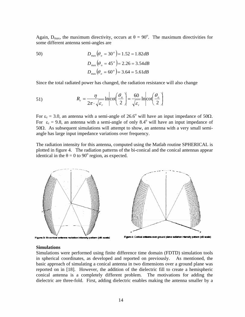
Again, Dmax, the maximum directivity, occurs at θ = 90o. The maximum directivities for some different antenna semi-angles are 50)
( ) dBD oo 82.152.130max ===θ
( ) dBD o 54.326.245maxo ===θ
Since the total radiated power has changed, the radiation resistance will also change 51) For εr = 3.0, an antenna with a semi-angle of 26.6o will have an input impedance of 50Ω. For εr = 9.8, an antenna with a semi-angle of only 8.4o will have an input impedance of 50Ω. As subsequent simulations will attempt to show, an antenna with a very small semi-angle has large input impedance variations over frequency.
( ) dBD oo 61.564.360max ===θ
⎟⎞
⎜⎛=⎟
⎞⎜⎛= cotln60cotln oo
rRθθη
⎠⎝⎠⎝⋅ 222 εεπ
The radiation intensity for this antenna, computed using the Matlab routine SPHERICAL is plotted in figure 4. The radiation patterns of the bi-conical and the conical antennas appear identical in the θ = 0 to 90o region, as expected.
imulations
ls d e
ns over a ground plane was ted on in [18] ill to create a hemispheric al antenna is a completely different problem. The motivations for adding the
ielectric are three-fold. First, adding dielectric enables making the antenna smaller by a
rr
SSimulations were performed using finite difference time domain (FDTD) simulation tooin spherical coordinates, as developed and reported on previously. As mentione , thasic approach of simulating a conical antenna in two dimensiob
reporonic
. However, the addition of the dielectric fcd
14
factor of (εr)1/2. This size reduction is significant enough to be a sufficient motivation by
difficult to break; an inverted cone is relatively elicate and easy to break off. The third reason for adding dielectric is to enable the design
antenna with a mo atch to 50Ω. The ution involves varyin θo, and the dielectric relative rmittivity, εr. The parameter to be optimized is the preservation of the shape of the UWB
ulse after transm sis is a me domain simulator (FDTD) in spherical coordinates.
e atching and fidelity in the time domain, any spurious reflections had to be eliminated. For this
ose, a perfectly matched layer (PML) was added to the simulation space at the rim of e simulation space. The PML was designed from first principles, as presented in [23],
t additional confusing factors.
he pulse transmission. The current at the ase of the antenna was calculated using (29) with the Hφ field averaged for all free space
tenna was calculated using
feed-line and “a” is the inner diameter. Here es at the antenna base. The antenna impedance in the
in / Iin.
51) are only valid for infinite antennas. pedance of the finite conical antenna exhibits strong
portant to consider these effects in designing any antenna for pedance presented in (51) is for an infinite antenna and is
r a wide frequency range, so matching to an input transmission line will require careful selection of the antenna characteristics to
ections over the entire 3.1-10.6GHz UWB band.
itself. The second reason for adding dielectric, is to make the antenna much more rugged. A hemisphere is relatively rugged anddof an stly omni-directional pattern that is also a good msol
eg both the antenna semi-angle,
pp ission from the antenna. The essential tool to enable this analyti
he development of the FDTD simulator in spherical coordinates closely followed Tm thodologies described in [17], [18], and [22]. In order to study antenna mpulse
urppth[24], and [25]. It consists of a set of 20 layers with a linearly increasing conductivity profile. The purpose of the PML is to simulate an infinite simulation space. That is, outgoing waves are absorbed by the PML layer structure and do not reflect back into the simulation space. Any waves present in the simulation space are due directly to antenna missions. In this manner, the antenna can be studied withoue
Antenna Input Impedance Another important parameter to be simulated and tracked is the antenna input impedance.
he antenna impedance was calculated during tTbangles. Similarly, the voltage at the base of the an 52) where “b” is the outer diameter of the coaxial the Eθ field is averaged over all anglsimulator is then calculated using Zin = V The input impedances calculated in (46) and (Practical antennas are finite, and the imfrequency dependence. It is imUWB applications. The input imonly valid on average for a finite antenna ove
minimize refl Input impedance of a conical antenna over a ground plane has been reported from measured structures [26]. The resistive input impedance exhibits about a 2:1 variation over a 2:1 frequency range, for an antenna 1λ tall with the wavelength chosen in the center of
( ) ( )abbEVin lnsin ⋅⋅⋅= θθ
15
the range. This 2:1 variation in input resistance is present in all conical antennas except for those much shorter than one wavelength, where it is more severe. The input impedance of a finite conical antenna over an infinite ground plane is [27] [28]: 53) with 54)
αβα
β
+
−=
1
1cin ZZ ⎥
⎦
⎤⎢⎣
⎡⎟⎠⎞
⎜⎝⎛=
2cotln60 o
r
cZθ
ε
and 55) with a being the spherical radius of the antenna, εr being the relative dielectric coefficient, θo the semi-angle of the antenna, Legn being the Legendre polynomial of order n, and hn
2 being the Hankel function of the second kind, order n.
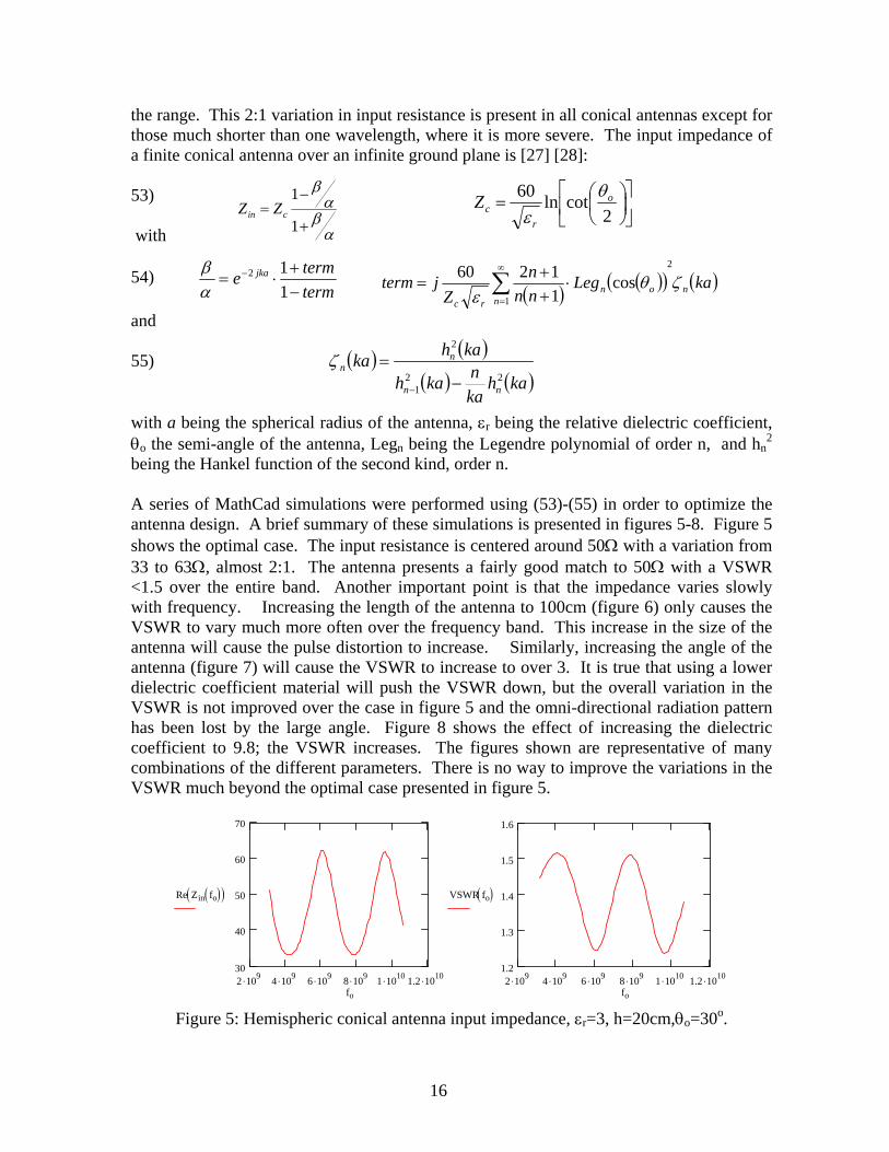
series of MathCad simulations were performed using (53)-(55) in order to optimize the Aantenna design. A brief summary of these simulations is presented in figures 5-8. Figure 5
he size of the a will cause the pulse distor ilarly, increasing the angle of the a (figure 7) will cause the VSWR to increase to over 3. It is true that using a lower
shows the optimal case. The input resistance is centered around 50Ω with a variation from 33 to 63Ω, almost 2:1. The antenna presents a fairly good match to 50Ω with a VSWR <1.5 over the entire band. Another important point is that the impedance varies slowly with frequency. Increasing the length of the antenna to 100cm (figure 6) only causes the
SWR to vary much more often over the frequency band. This increase in tVantennntenn
tion to increase. Simadielectric coefficient material will push the VSWR down, but the overall variation in the VSWR is not improved over the case in figure 5 and the omni-directional radiation pattern has been lost by the large angle. Figure 8 shows the effect of increasing the dielectric oefficient to 9.8; the VSWR increases. The fic
combinations of the different parameters. There is no way to improve the variations in the VSWR much beyond the optimal case presented in figure 5.
Simulation Results: Unmatched Antenna ulation results will first be viewed for the case of a poorly matched antenna. For all
ages, the view is a three dimensional perspective of a two dimensional cross section of the simulation space of the antenna. The simulation was performed in sphericcoordinates, and then re-mapped to Cartesian coordinates. The re-mapping process produces some graininess and minor artifacts, especially at the outer edges of the
ispheric simulation region and along the axis of symmetry of the antenna. In all ages, the antenna is a small cone at the bottom center of the view, and the metal po
antenna is surrounded by a hemisphere of dielectric material of an equal radius t
2 .109 4 .109 6 .109
60 1.4
8 .10930
1 .1010 1.2 .1010
40
50
1.2
1.3
Re Zin fo( )( )
fo2 .109 4 .109 6 .109 8 .109 1 .1010 1.2 .1010
1.1
VSWR fo( )
fo
2 .109 4 .109 6 .109 8 .109 1 .1010
15
30
1.2 .101010
20
25
Re Zin fo( )( )
fo2 .109 4 .109 6 .109 8 .109 1 .1010 1.2 .1010
1.5
2
3.5
2.5
3
VSWR fo( )
fo
2 .109 4 .109 6 .109 8 .109 1 .1010 1.2 .101015
20
25
30
35
Re Zin fo( )( )
fo2 .109 4 .109 6 .109 8 .109 1 .1010 1.2 .10101
1.5
2
2.5
3
VSWR fo( )
fo
17
me
tric
sim
mism face. e and
B a
9)
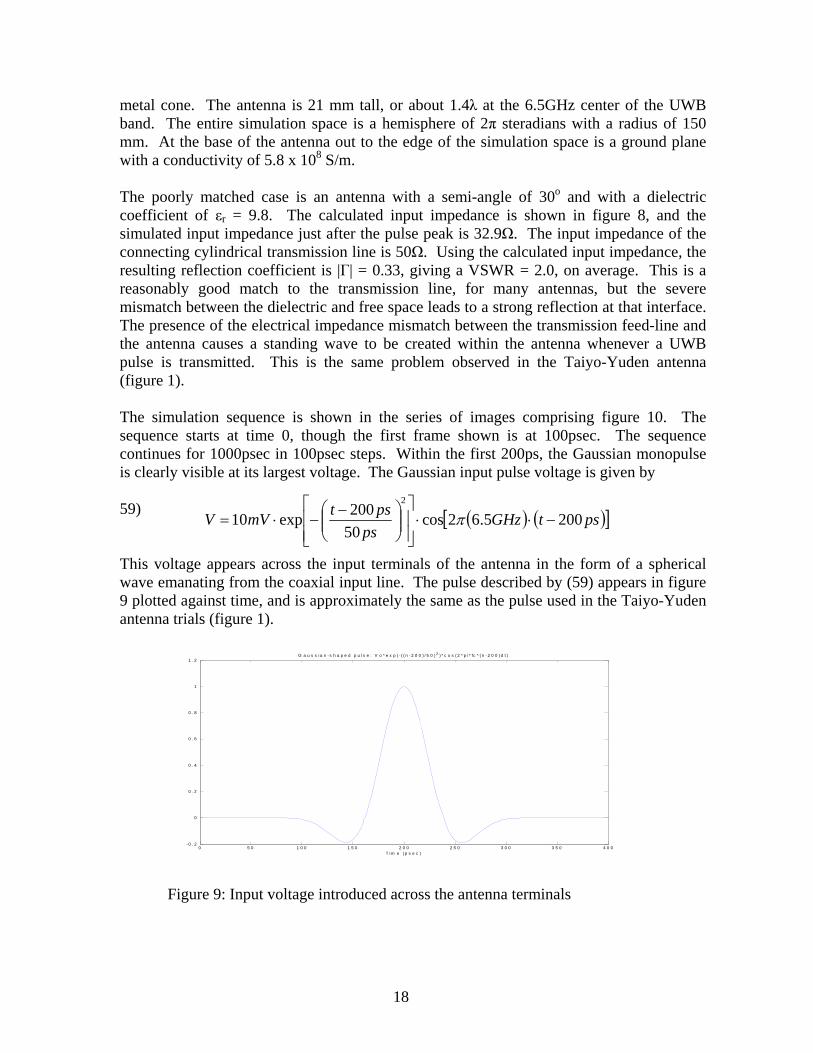
h wave emanating from the coaxial input line. The pulse described by (59) appears in 9 plotted against time, and is approximately the same as the pulse used in the Taiyo-Yuden antenna trials (figure 1).
Figure 9: Input voltage introduced across the antenna terminals
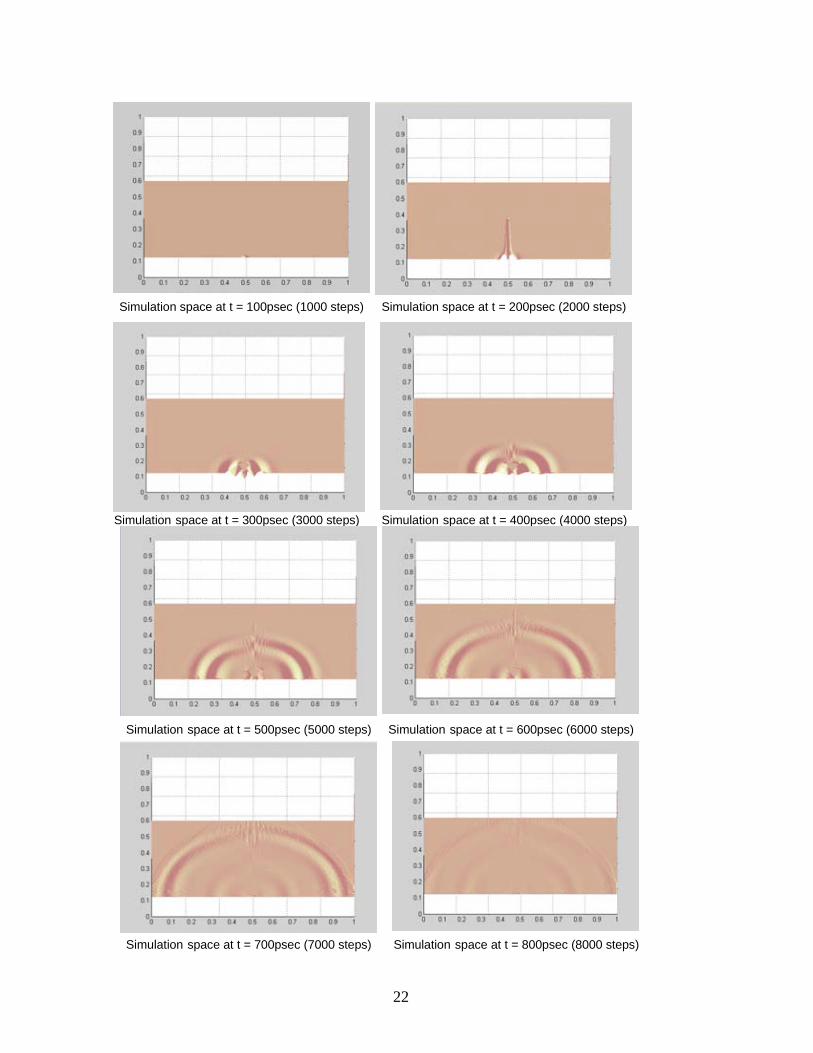
tal cone. The antenna is 21 mm tall, or about 1.4λ at the 6.5GHz center of the UWB band. The entire simulation space is a hemisphere of 2π steradians with a radius of 150 mm. At the base of the antenna out to the edge of the simulation space is a ground plane with a conductivity of 5.8 x 10⁸ S/m.
The poorly matched case is an antenna with a semi-angle of 30o and with a dieleccoefficient of εr = 9.8. The calculated input impedance is shown in figure 8, and the
ulated input impedance just after the pulse peak is 32.9Ω. The input impedance of the connecting cylindrical transmission line is 50Ω. Using the calculated input impedance, the resulting reflection coefficient is |Γ| = 0.33, giving a VSWR = 2.0, on average. This is a reasonably good match to the transmission line, for many antennas, but the severe
atch between the dielectric and free space leads to a strong reflection at that interThe presence of the electrical impedance mismatch between the transmission feed-linthe antenna causes a standing wave to be created within the antenna whenever a UWpulse is transmitted. This is the same problem observed in the Taiyo-Yuden antenn(figure 1).
The simulation sequence is shown in the series of images comprising figure 10. The sequence starts at time 0, though the first frame shown is at 100psec. The sequence continues for 1000psec in 100psec steps. Within the first 200ps, the Gaussian monopulse is clearly visible at its largest voltage. The Gaussian input pulse voltage is given by
5 This voltage appears across the input terminals of the antenna in the form of a sp
G a u s s i a n - s h a p e d p u l s e : V o * e x p ( - ( ( n - 2 0 0 ) / 5 0 ) 2 ) * c o s ( 2 * p i * fc * ( n - 2 0 0 ) d t )
18
By 300ps the front edge of the pulse is beginning to strike the dielectric-space interface, and b . A
anding wave is established within the antenna and is clearly visible by 600ps. The wave e produces a wave which travels back into the
in the antenna is one of the most severe cases vestigated for this work, and it indicates the importance of carefully matching the
y 400ps the main portion of the wave has passed out of the antenna and into spacestreflection at the dielectric-free space interfactransmission line. The mismatch between the antenna and the transmission line produces a second reflection, and the resulting standing wave dampens out very slowly. By 800ps the standing wave within the antenna is still strong, and the spherical space behind the Gaussian monopulse is filled with echoes emanating from the standing wave within the antenna. By 1000ps, the main Gaussian electromagnetic pulse has been absorbed by the PML layer surrounding the simulation space, but the dielectric volume of the antenna still contains a noticeable standing wave. This standing wave continues to emit electromagnetic oscillations into space, in effect, following behind the Gaussian electromagnetic wave. This is the same problem seen in the Taiyo-Yuden antenna (figure 1) and is indicative of the extreme sensitivity of UWB antennas to impedance mismatches. The standing wave generated withinimpedance of the antenna to its feed line. It indicates that there are many ways of building a poorly functioning version of this antenna just by varying the antenna semi-angle, θo, and the dielectric permittivity, εr. The antenna must be well matched to the input transmission line, especially if the relative dielectric permittivity of the antenna is large, as it is with this antenna. The conclusion is that this antenna is not useful for UWB communications, since the trailing oscillations behind the Gaussian monopulse will corrupt subsequent UWB pulses used for communicating information.
19
20
Simulation space at t = 100psec (1000 steps) Simulation space at t = 200psec (2000 steps)
Simulation space at t = 300psec (3000 steps) Simulation space at t = 400psec (4000 steps)
Simulation space at t = 500psec (5000 steps) Simulation space at t = 600psec (6000 steps)
Simulation space at t = 700psec (7000 steps) Simulation space at t = 800psec (8000 steps)
Simulation Results: Matched Antenna The FDTD simulator was run for a wide variety of different antenna combinations in an effort to find the antenna with the best match to the 50Ω input transmission line. The best combination was found to be an antenna with a semi-angle of 30o and a dielectric constant of εr = 3.0. The antenna was 2.1cm tall, slightly less than one wavelength at the 6.5GHz center of the UWB band, but equal to the length shown in the previous example. The simulation space was again the 150cm upper hemisphere. The antenna was driven with the same Gaussian monopulse that was used in the previous example. For the first 400ps the results are similar those of the last simulation. The Gaussian monopulse appears at its peak value by 200ps, and by 400ps the pulse has left the antenna dielectric. The wave reflected from the dielectric-space interface is smaller than for the previous example, since the dielectric coefficient is εr = 3.0 instead of εr = 9.8. This means that driving impedance mismatches will be less noticeable with this antenna than with the antenna of the previous example. This is apparent by the smaller internally reflected waves within the first 600ps. By 500ps a significant reflected wave is visible within the antenna dielectric returning towards the coaxial drive terminal. By 600ps, the internally reflected wave has been mostly absorbed by the nearly matched 50Ω input transmission line impedance. Figure 5 gives an average antenna input resistance of 50Ω, but the simulator calculates 45.6Ω, giving |Γ| = 0.046 and VSWR = 1.1. At 600ps, a partially reflected wave has reversed its course away from the feed-line and is on its way out of the antenna dielectric. The input driver is modeled as a 50Ω transmission line, so the effects of an impedance mismatch will occur at the antenna/ feed-line interface. By 700ps, it is apparent that there is a small reflected wave following behind the main Gaussian monopulse. This is the only reflected wave visible in the entire sequence that escapes the antenna and propagates. It results from the imperfect impedance match between the antenna and its 50Ω feed-line. A second reflected wave occurring from the mismatch between the dielectric-space interface is visible at 700 and 800ps. This wave is adequately absorbed by the input transmission line, and any further reflections are of too small amplitude to be visible. The primary wave is absorbed in the PML region of the simulation space by 900ps, and all waves have either been absorbed by the PML region or the drive impedance by 1000ps, as desired.
Simulation space at t = 900psec (9000 steps) Simulation space at t = 1000psec (10000 steps)
21
22
Simulation space at t = 200psec (2000 steps)
S
Simulation space at t = 100psec (1000 steps)
imulation space at t = 300psec (3000 steps) Simulation space at t = 400psec (4000 steps)
Simulation space at t = 500psec (5000 steps) Simulation space at t = 600psec (6000 steps)
Simulation space at t = 700psec (7000 steps) Simulation space at t = 800psec (8000 steps)
Simulation space at t = 900psec (9000 steps) Simulation space at t = 1000psec (10000 steps
Simulation of UWB antenna, 2.1cm tall, semi-angle = 30o, er = 3.0, Zin = 45O
)
Conclusion A basic design for a dielectrically filled conical UWB antenna, dubbed the hemispheric conical antenna, was presented. FDTD simulation results, along with input impedance calculations for such an antenna were reviewed. A final design for a hemispheric conical antenna was presented. The final, optimized antenna was designed for the FCC UWB band from 3.1-10.6GHz. It is 2.1cm tall, with an εr = 3.0 and a semi-angle of θr = 30o
an average VSWR = 1.35 with a maximum VSWR = 1.5. Time domain simulations indicate a small trailing pulse behind the Gaussian UWB pulse, but no standing waves were evident. The critical importance of time domain simulations for investigations of UWB antennas was presented. The simulation results point to a design; fabrication of that design may indicate the need for small variations in the design parameters to achieve optimal UWB pulse transmission. Results for this antenna appear promising, and it ma offer better pulse fidelity than the other physically constrained UWB antennas in the literature.
, giving it
y
23
References ) K.K O, et al, “On-Chip Antennas in Silicon ICs and Their Application,” IEEE Trans. on Elec.
Devices, vol. 52, no. 7, Jul. 2005, pp. 1312-1323. ) M.T. Chyssomallis and C.G. Christodoulou, “Antennas for Mobile Communications,” Wiley
Encyclopedia of Telecommunications, J.G Proakis (ed.), John Wiley and Sons, 2003, pp. 1-12. ) W. Choi, S. Kwon, and B. Lee, “Ceramic Chip Antenna using Meander Conductor Lines,”
Elec. Letters, vol. 37, no. 15, 19th Jul., 2001, pp. 933.-934. ) P.M Mendes, et al, “Design of a Folded-Patch Chip-Size Antenna for Short-Range
Communications,” 33rd Euro. Microwave Conf. Munich, vol. 2, 7-9 Oct. 2003, pp. 723-726. ) C.C. Lin, Y.J. Chang, H.R. Chuang, “Design of a 900/1800MHz Dual-band LTCC Chip
Antenna for Mobile Communications Applications,” Microwave Journal, vol. 47, no. 1, Jan. 2004, pp. 203-207.
) K. Fujimoto, et al, Small Antennas, Research Studies Press, Ltd., 1987, pp. 1-29. ) R.A. Burberry, “Electrically Small Antennas,” IEE Colloquium on Elec. Small Antennas, 23
Oct., 1990, pp. 1-5. , “Low Q Electrically Small Linear and Elliptical Polarized Spherical Dipole
1
2
3
4
5
6
78
9) S.R. BestAntennas,” IEEE Trans. on Antennas and Prop., vol. 53, no. 3, Mar. 2005, pp. 1047-1053.
10) J.S. McLean, “The Radiative Properties of Electrically-Small Antennas,” IEEE Int’l Symp. on Electromagnetic Compatibility, Symp. Record, 22-26 Aug., 1994, pp. 320-324.
11) D.H. Kwon, et al, “A Small Ceramic Chip Antenna for Ultra-Wideband Systems,” IEEE Joint Conf. on UWB Sys. And Tech, 18-21 May, 2004, pp. 307-311.
12) L. Schreider, et al, “Archimedean Microstrip Spiral Antenna Loaded by Chip Resistors Inside the Substrate,” Antennas and Prop. Society Int’l Symp., vol 1, 20-25 Jun 2004, pp. 1066-1069.
13) H. Okado, M. Aoki, M. Horie, “Antenna for Ultra Wideband System,” IEEE 802.15-03/145r0 online documents, Mar. 2003, presented at the IEEE 802.15 working group plenary meeting in Dallas, TX, USA. [online] http://grouper.ieee.org/groups/802/15/pub/2003/Mar03/03145r0p802-15TG3%a-TRDA-TaiyoYuden-CFP-Presentation.ppt.
14) V. Stoiljkovic and P. Webster, “A Novel Low-Cost Chip Antenna for Short-Range Radio Applications,” IEEE Antennas and Prop. Soc. Symp., vol. 1, 2004, pp. 1058-1061.
15) R. Lawton and A. Ondrejka, “Antennas and the Associated Time-Domain Range for the Measurement of Impulsive Fields”, Nat. Bur. of Stnds. Tech.l Note 1008, Boulder CO, Nov. 1978.
16) J.R. Andrews, “UWB Signal Sources, Antennas, and Propagation”, Picosecond Pulse Labs Appl. Note, AN-14a, Aug. 2003, pp. 3.
17) R. Holland, “THREDS: A Finite Difference Time-Domain EMP Code in 3D Spherical Coordinates”, IEEE Trans. on Nucl. Sci., vol. NS-30, no. 6, Dec. 1983, pp. 4592-4595.
18) G. Liu and C.A. Grimes, “Spherical-Coordinate FDTD Analysis of Conical Antennas Mounted Above Finite Ground Planes”, Microwave and Opt. Tech. Let., vol. 23, no. 2, Oct. 1999, pp. 78-82.
19) FCC 02-48, “Revision of Part 15 of the Commission’s Rules Regarding Ultra-Wideband Transmission Systems”, First Report and Order, Wash. D.C., adopted Feb. 14, 2002, released April 22, 2002.
20) Ramo, Whinnery, and Van Duzer, Fields and Waves in Communication Electronics, John Wiley and Sons, 1965, p. 464.
21) M. Fusco, “FDTD Algorithm in Curvilinear Coordinates”, IEEE Trans. On Ant. and Prop., vol. 38, no. 1, Jan. 1990, pp. 76-89.
23) J.P. Berenger, “A Perfectly Matched Layer for the Absorption of Electromagnetic Waves,”
24) DTD Solution of Wave-Structure Interaction
EE Microwave and Guided Wave
26) ill,
27) rop., vol. 47, no. 3, Mar. 1994, pp. 436-439.
. 11, Nov. 1949, pp. 1269-1271.
Journal of Computational Physics, no. 114, 1994, pp. 185-200. J.P. Berenger, “Perfectly Matched Layer for the FProblems,” IEEE Transactions on Antennas and Propagation, vol 44, no. 1, Jan. 1996, pp. 110-117.
25) D.S. Katz, et al, “Validation and Extension to Three Dimensions of the Berenger PML Absorbing Boundary Condition for FD-TD Meshes,” IELetters, vol. 4, no. 8, Aug. 1994, pp. 268-270. Harvard Radio Research Laboratory Staff, “Very High Frequency Techniques,” McGraw-HNew York and London, 1947, vol. 1, pp. 102-110. S.S. Sandler and R.W.P. King, “Compact Conical Antennas for Wide-Band Coverage”, IEEE Trans. on Ant. and P
28) C.H. Papas and R.W.P. King, “Input Impedance of Wide-Angle Conical Antennas Fed by a Coaxial Line,” Proc. IRE, vol. 37, no
25
Dis
1
1
tribution
MS0874 Robert W. Brocato, 1711 M1 S0874 David W. Palmer, 1711
1 MS0874 Gregg A. Wouters, 1711 MS9104 Jack L. Skinner, 8226 MS9960 Central Technical Files, 892 45-1