19
| Date post: | 18-Nov-2014 |
| Category: |
Documents |
| Upload: | vivek-gangwar |
| View: | 397 times |
| Download: | 4 times |

CONTENTS INTRODUCTION HISTORY DEVICE STRUCTURE FABRICATION WORKING PRINCIPLE TYPES OF HEMTS GROWTH CHARACTERSTICS ADVANTAGES APPLICATIONS CONCLUSION

INTRODUCTION
High Electron Mobility Transistors (HEMTs) have
emerged as a promising candidate for microwave (f > 1
GHz) power amplification with applications ranging from
satellite links to wireless communications, from highways
to electronic warfare.
HEMTs were primarily based on AlGaAs/GaAs,
AlGaAs/InGaAs, AlInAs/InGaAs and related epitaxial
films grown on GaAs or InP substrates.
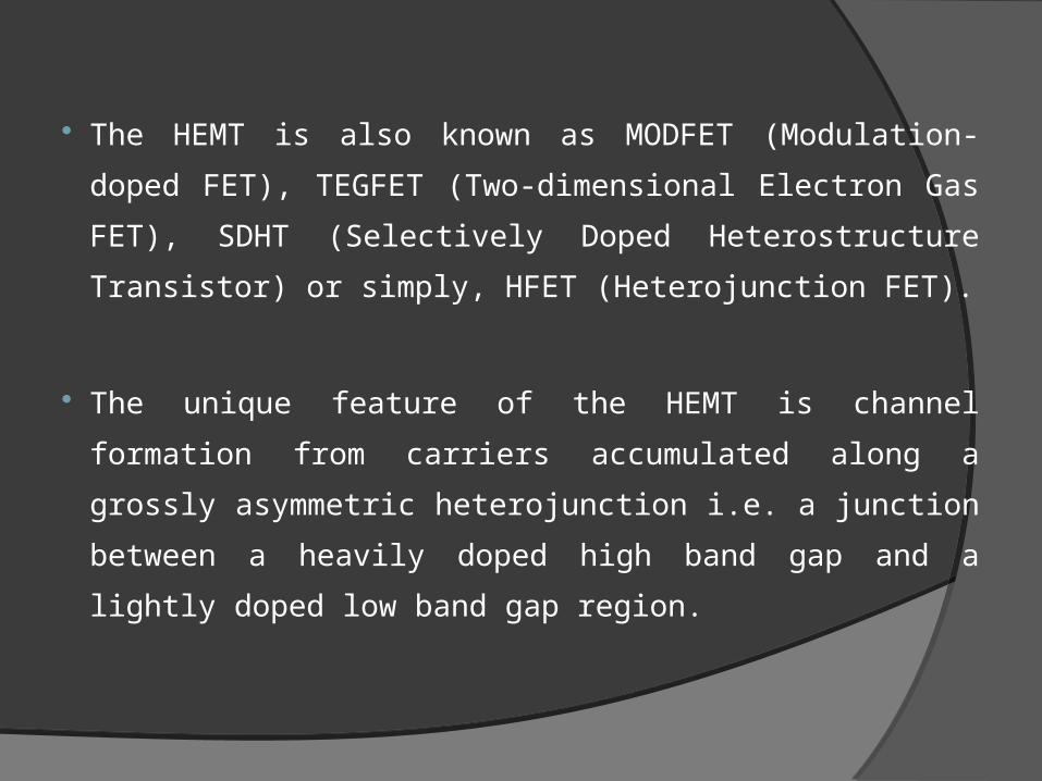
The HEMT is also known as MODFET (Modulation-
doped FET), TEGFET (Two-dimensional Electron Gas
FET), SDHT (Selectively Doped Heterostructure
Transistor) or simply, HFET (Heterojunction FET).
The unique feature of the HEMT is channel formation
from carriers accumulated along a grossly asymmetric
heterojunction i.e. a junction between a heavily doped
high band gap and a lightly doped low band gap region.

HISTORY The physics of carrier transport parallel to a heterojunction
was first considered in 1969.
First demonstrated in AlGaAs/GaAs hetero junctions in
1979, and applied to demonstrate a HEMT in 1980. Electron
mobility enhancement at AlGaN/GaN heterojunction was
first reported in 1991.
Enhancement was attributed to the 2D nature of the
electrons, based on observations of mobility increase
with lowering of the temperature.

DEVICE STRUCTURE
We have fabricated AlGaN/GaN HFETs with the
source-to-drain spacing from 2 µm to 7 µm, the gate
length from 0.25 µm to 5 µm and the total gate width
from 50 µm to 150 µm (2×25 µm to 2×75 µm).
This reduces the parasitic source inductance and
improves thermal dissipation.
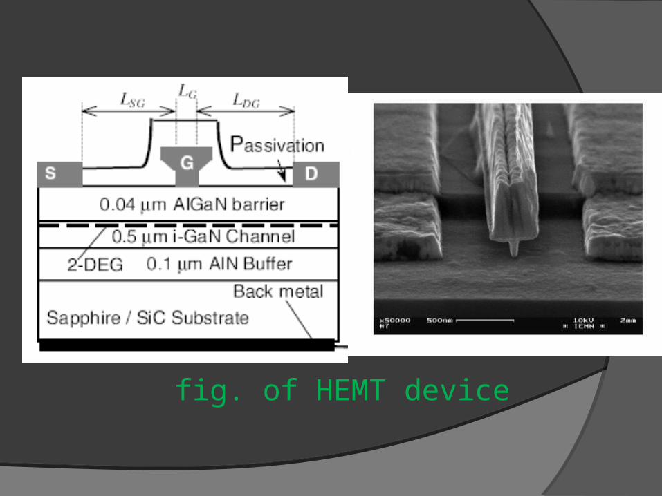
fig. of HEMT device

FABRICATION The Substrate:- Sapphire (Al2O3) and SiC are the most
popular substrate materials used currently. Sapphire
substrates are cheaper for GaN growth than SiC.
The Contacts:- The shape of the gate contact is
crucial to device performance. T- or Y shaped
cross-sections are employed.

Growth of the semiconductor epitaxial and
insulator layers.
Photolithography for ohmic contact openings.
Ohmic contact metallization.
Rapid Thermal Annealing (RTA) of ohmic
contacts.
Photolithography for device isolation level.
Reactive ion etching or ion implantation for
device isolation.

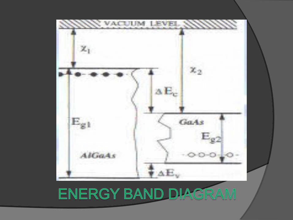
WORKING PRINCIPLE Charge transfer takes place across the interface to equalize
the Fermi energy on both sides. Electrons from the donor
impurities of the highly doped n-type Ga1-xAlxAs are
transferred to the conduction band of the nearly intrinsic p-
type GaAs.
Positively charged donor ions are therefore left near the
interface on the n-type side and negatively charged acceptor
ions are left near the interface on the p-type side
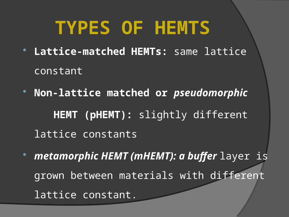
TYPES OF HEMTS Lattice-matched HEMTs: same lattice constant
Non-lattice matched or pseudomorphic
HEMT (pHEMT): slightly different lattice
constants
metamorphic HEMT (mHEMT): a buffer layer
is grown between materials with different lattice
constant.
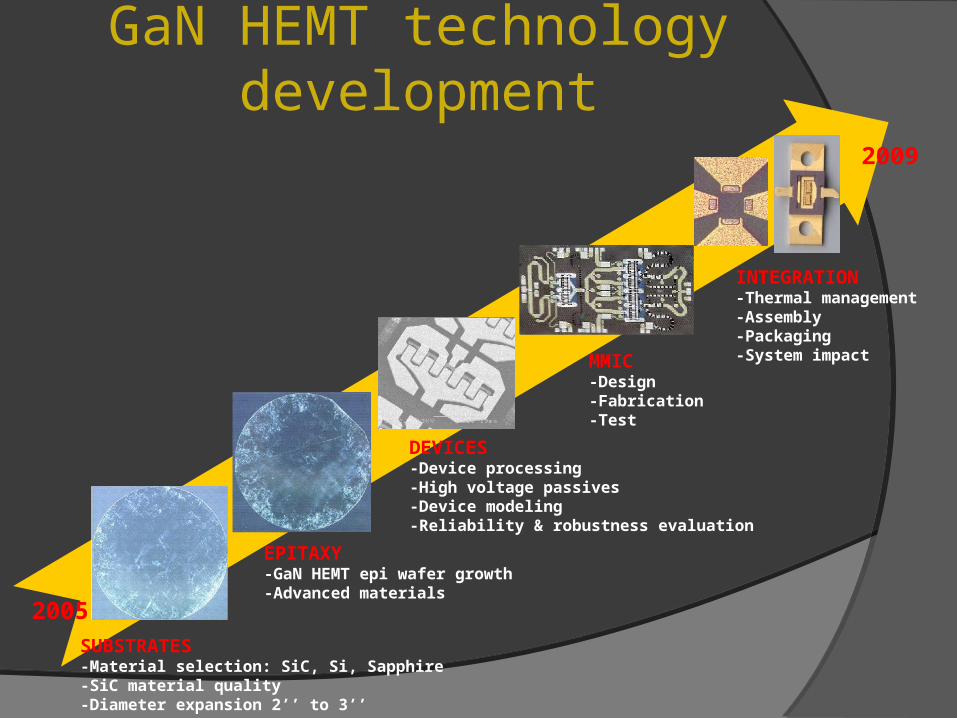
GaN HEMT technology development
SUBSTRATES-Material selection: SiC, Si, Sapphire-SiC material quality-Diameter expansion 2’’ to 3’’
EPITAXY-GaN HEMT epi wafer growth-Advanced materials
DEVICES-Device processing-High voltage passives-Device modeling-Reliability & robustness evaluation
MMIC-Design-Fabrication-Test
INTEGRATION-Thermal management-Assembly-Packaging-System impact
2005
2009

CHARACTERSTICS DRAIN CURRENT
CHARACTERSTICS:
The measured DC
characteristics of a
power HEMT are
shown in Fig.
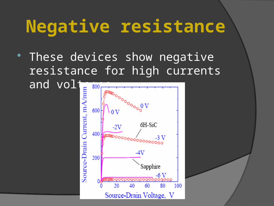
Negative resistance
These devices show negative resistance for high currents and voltages.
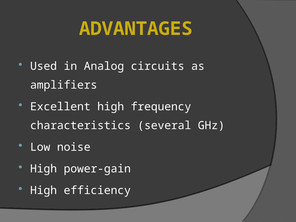
ADVANTAGES
Used in Analog circuits as amplifiers
Excellent high frequency characteristics
(several GHz)
Low noise
High power-gain
High efficiency
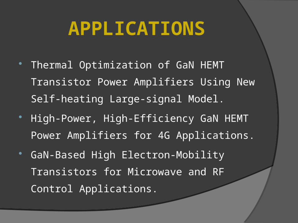
APPLICATIONS
Thermal Optimization of GaN HEMT
Transistor Power Amplifiers Using New Self-
heating Large-signal Model.
High-Power, High-Efficiency GaN HEMT
Power Amplifiers for 4G Applications.
GaN-Based High Electron-Mobility Transistors
for Microwave and RF Control Applications.
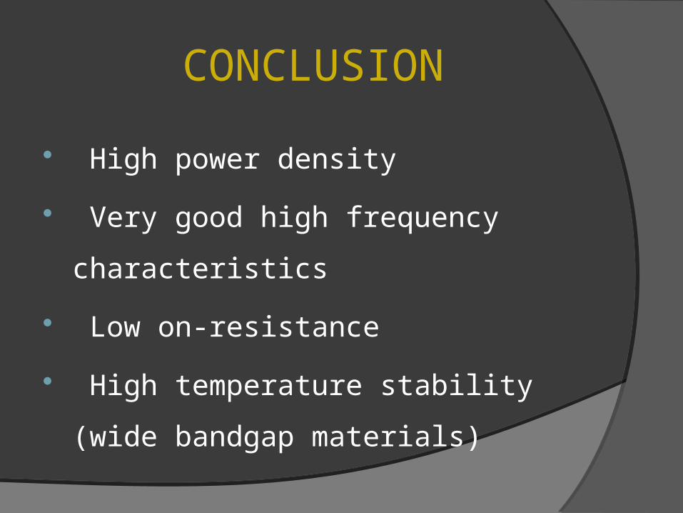
CONCLUSION
High power density
Very good high frequency
characteristics
Low on-resistance
High temperature stability (wide
bandgap materials)

THANKS…and Queries.. ?


