27
Hermes Microvision, Inc. Investor Presentation November 2013
Hermes Microvision, Inc. Investor PresentationNovember 2013
I. Introduction to HMI
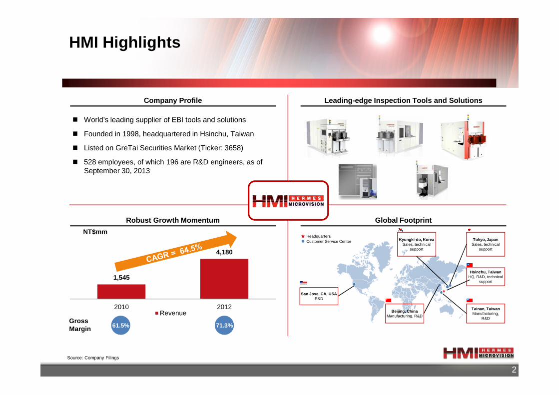
HMI Highlights
Company Profile Leading-edge Inspection Tools and Solutions
� World’s leading supplier of EBI tools and solutions
� Founded in 1998, headquartered in Hsinchu, Taiwan
� Listed on GreTai Securities Market (Ticker: 3658)
� 528 employees, of which 196 are R&D engineers, as of September 30, 2013
2
Global FootprintRobust Growth Momentum
Gross Margin 71.3%61.5%
San Jose, CA, USAR&D
Tokyo, JapanSales, technical
support
Kyungki-do, KoreaSales, technical
support
Tainan, TaiwanManufacturing,
R&D
Beijing, ChinaManufacturing, R&D
Customer Service CenterHeadquarters
Hsinchu, TaiwanHQ, R&D, technical
support
Source: Company Filings
1,545
4,180
2010 2012
NT$mm
Revenue
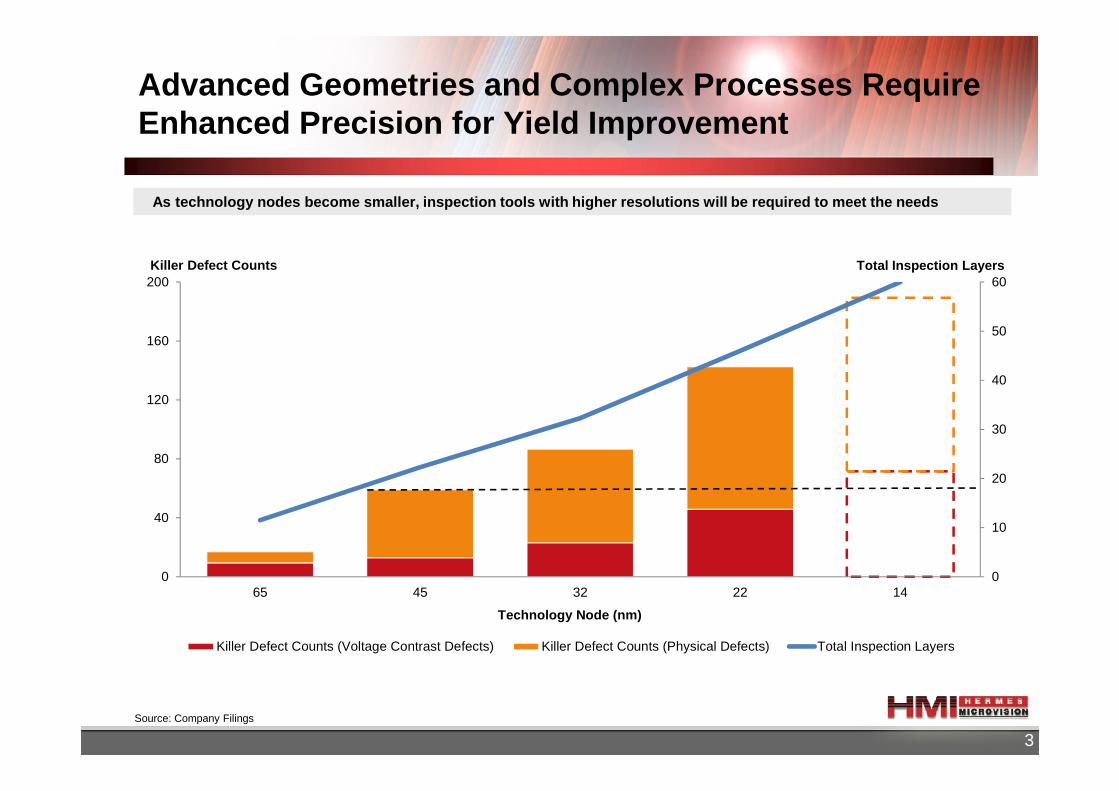
As technology nodes become smaller, inspection tool s with higher resolutions will be required to meet the needs
Advanced Geometries and Complex Processes Require Enhanced Precision for Yield Improvement
40
50
60
120
160
200Total Inspection LayersKiller Defect Counts
3Source: Company Filings
0
10
20
30
0
40
80
120
65 45 32 22 14
Killer Defect Counts (Voltage Contrast Defects) Killer Defect Counts (Physical Defects) Total Inspection Layers
Technology Node (nm)
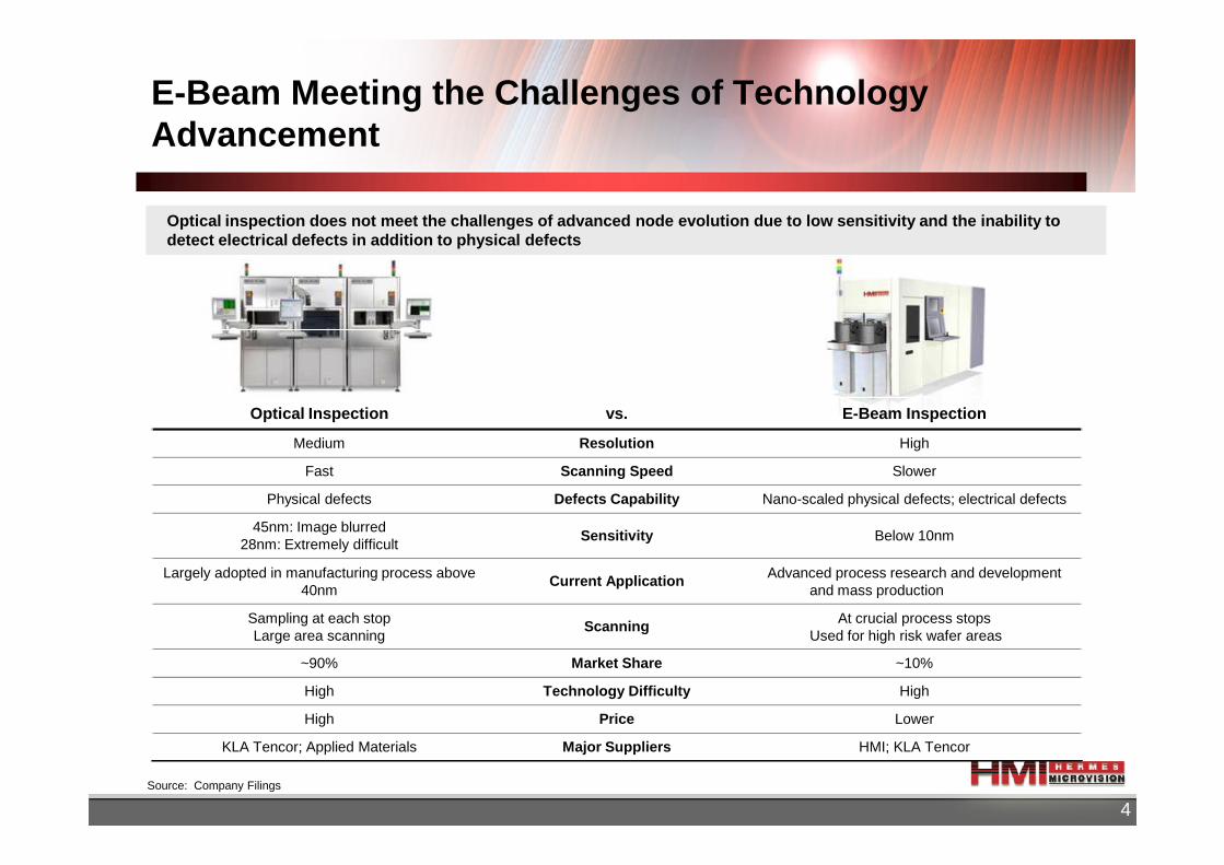
Optical inspection does not meet the challenges of advanced node evolution due to low sensitivity and the inability to detect electrical defects in addition to physical d efects
E-Beam Meeting the Challenges of Technology Advancement
Optical Inspection vs. E-Beam Inspection
4
Medium Resolution High
Fast Scanning Speed Slower
Physical defects Defects Capability Nano-scaled physical defects; electrical defects
45nm: Image blurred28nm: Extremely difficult
Sensitivity Below 10nm
Largely adopted in manufacturing process above 40nm
Current Application Advanced process research and development and mass production
Sampling at each stop Large area scanning
Scanning At crucial process stops Used for high risk wafer areas
~90% Market Share ~10%
High Technology Difficulty High
High Price Lower
KLA Tencor; Applied Materials Major Suppliers HMI; KLA Tencor
Source: Company Filings
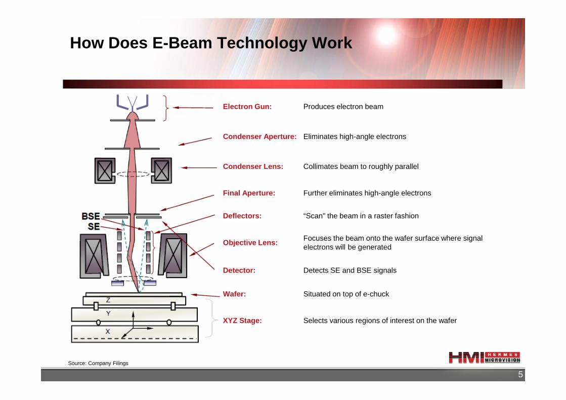
How Does E-Beam Technology Work
Electron Gun: Produces electron beam
Condenser Aperture: Eliminates high-angle electrons
Condenser Lens: Collimates beam to roughly parallel
Final Aperture: Further eliminates high-angle electrons
5
Deflectors: “Scan" the beam in a raster fashion
Objective Lens:Focuses the beam onto the wafer surface where signal electrons will be generated
Detector: Detects SE and BSE signals
Wafer: Situated on top of e-chuck
XYZ Stage: Selects various regions of interest on the wafer
Source: Company Filings
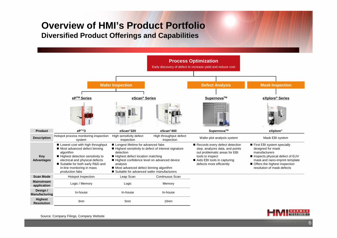
Overview of HMI’s Product PortfolioDiversified Product Offerings and Capabilities
Process OptimizationEarly discovery of defect to increase yield and reduce cost
Wafer Inspection Defect Analysis Mask Inspection
ePTM Series eScan® Series Supernova TM eXplore ® Series
6Source: Company Filings, Company Website
Product eP TM3 eScan®320 eScan®400 Supernova TM eXplore ®
DescriptionHotspot process monitoring inspection
systemHigh sensitivity defect
inspection High throughput defect
inspectionWafer plot analysis system Mask EBI system
Key Advantages
� Lowest cost with high throughput� Most advanced defect binning
algorithm� Highest detection sensitivity to
electrical and physical defects � Suitable for both early R&D and
in-line monitoring in mass production fabs
� Longest lifetime for advanced fabs� Highest sensitivity to defect of interest signature
detection � Highest defect location matching� Highest confidence level on advanced device
analysis� Most advanced defect binning algorithm� Suitable for advanced wafer manufacturers
� Records every defect detection step, analyzes data, and points out problematic areas for EBI tools to inspect
� Aids EBI tools in capturing defects more efficiently
� First EBI system specially designed for mask manufacturers
� Inspects physical defect of EUV mask and nano-imprint template
� Offers the highest inspection resolution of mask defects
Scan Mode Hotspot Inspection Leap Scan Continuous Scan
Mainstream application
Logic / Memory Logic Memory
Design / Manufacturing
In-house In-house In-house
Highest Resolution
3nm 5nm 10nm
II. Key Investment Highlights
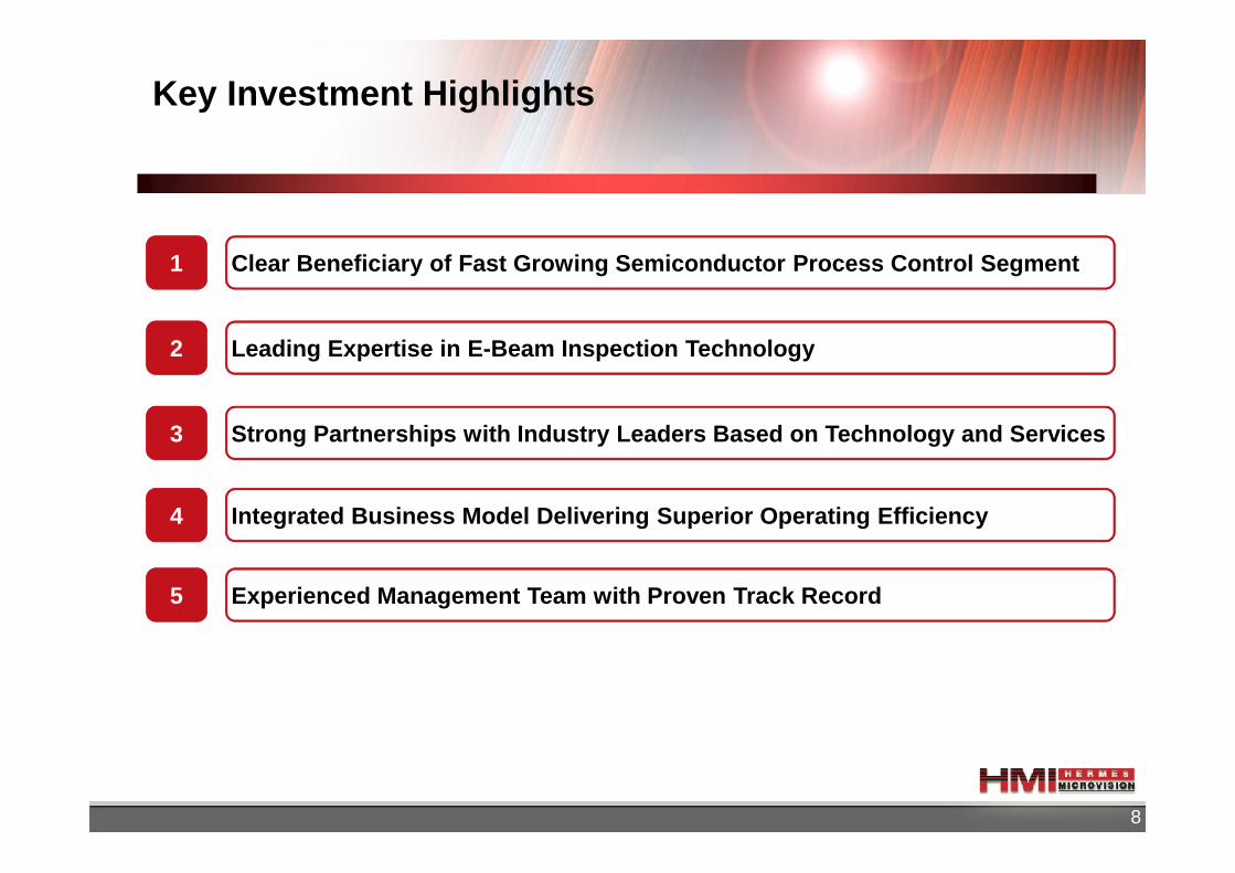
Key Investment Highlights
1 Clear Beneficiary of Fast Growing Semiconductor Pro cess Control Segment
2 Leading Expertise in E-Beam Inspection Technology
3 Strong Partnerships with Industry Leaders Based on Technology and Services
8
3 Strong Partnerships with Industry Leaders Based on Technology and Services
4 Integrated Business Model Delivering Superior Opera ting Efficiency
5 Experienced Management Team with Proven Track Recor d
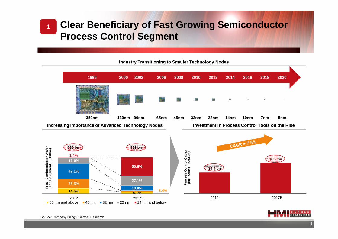
1995 2000 2002 2006 2008 2010 2012 2014 2016 2018 2020
Industry Transitioning to Smaller Technology Nodes
350nm 130nm 90nm 65nm 45nm 32nm 28nm 14nm 10nm 7nm 5nm
1 Clear Beneficiary of Fast Growing Semiconductor Process Control Segment
9
$4.4 bn
$6.3 bn
2012 2017
14.6% 5.1%
26.3%
3.4%
42.1%
13.8%
15.6%
27.1%
1.4%
50.6%
2012 201765 nm and above 45 nm 32 nm 22 nm 14 nm and below
350nm 130nm 90nm 65nm 45nm 32nm 28nm 14nm 10nm 7nm 5nm
Source: Company Filings, Gartner Research
Increasing Importance of Advanced Technology Nodes
$30 bn $39 bn
Tot
al S
emic
ondu
ctor
Waf
er
Fab
Equ
ipm
ent
(U
S$b
n)
Investment in Process Control Tools on the Rise
Pro
cess
Con
trol
Cap
ex
(incl
. OE
M)
(U
S$b
n)
E E
2012 2014E
E-Beam10%
E-Beam
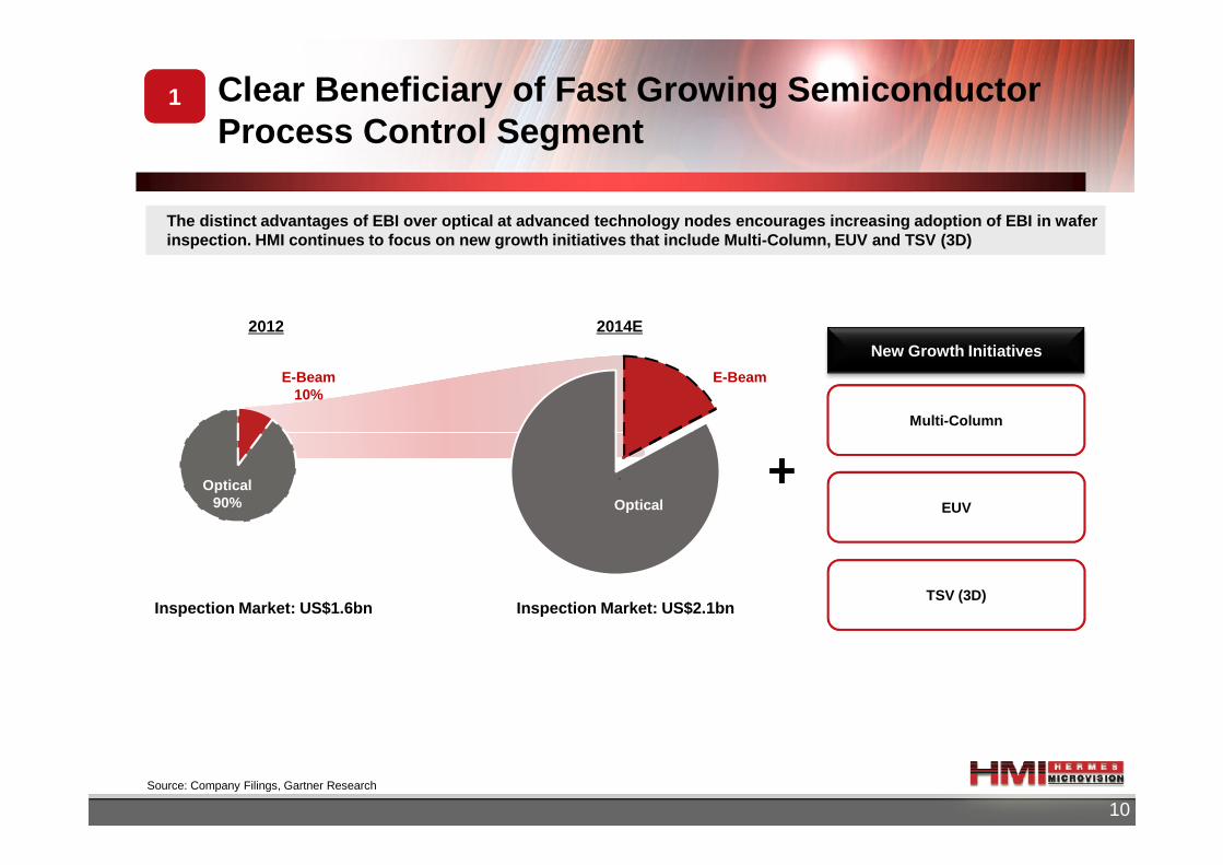
1 Clear Beneficiary of Fast Growing Semiconductor Process Control Segment
New Growth Initiatives
The distinct advantages of EBI over optical at adva nced technology nodes encourages increasing adoptio n of EBI in wafer inspection. HMI continues to focus on new growth in itiatives that include Multi-Column, EUV and TSV (3 D)
Multi-Column
10
` +
Source: Company Filings, Gartner Research
Optical90% Optical
Inspection Market: US$1.6bn Inspection Market: US$2. 1bn
EUV
TSV (3D)
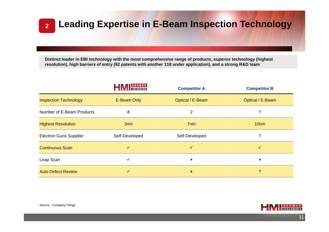
Competitor A Competitor B
Inspection Technology E-Beam Only Optical / E-Beam Optical / E-Beam
Number of E-Beam Products 8 2 ?
Distinct leader in EBI technology with the most com prehensive range of products, superior technology ( highest resolution), high barriers of entry (92 patents wit h another 118 under application), and a strong R&D team
2 Leading Expertise in E-Beam Inspection Technology
11
Highest Resolution 3nm 7nm 10nm
Electron Guns Supplier Self-Developed Self-Developed ?
Continuous Scan � � �
Leap Scan � � �
Auto Defect Review � � ?
Source: Company Filings
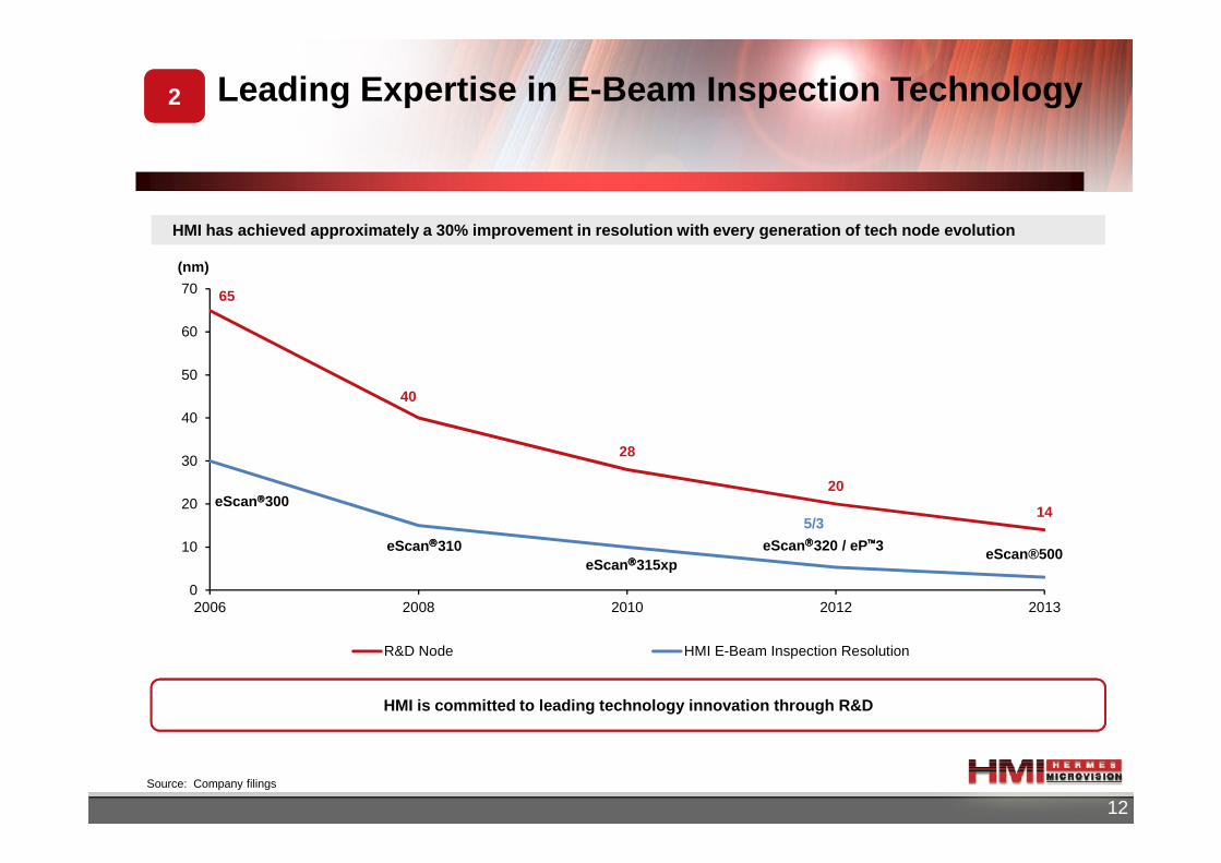
HMI has achieved approximately a 30% improvement in resolution with every generation of tech node evol ution
2 Leading Expertise in E-Beam Inspection Technology
65
4040
50
60
70
(nm)
12
HMI is committed to leading technology innovation t hrough R&D
Source: Company filings
28
20
145/3
0
10
20
30
2006 2008 2010 2012 2013
R&D Node HMI E-Beam Inspection Resolution
eScan300
eScan310eScan315xp
eScan320 / eP3 eScan®500

Company Revenue
$49,089
28,622
11,111
10,610
9,152
8,965
8,415
6,917
Strong Partnerships with Industry Leaders Based on Technology and Services
� HMI teams up with customers in R&D and shares the benefits of innovation
� HMI customizes to meet different needs
� HMI provides instant customer service globally
3
Top IDMs 1 by 2012 Rev. (US$mm)
HMI’s Winning Business ModelPartnerships for Long-term Success
13
Company Revenue
$17,130
4,200
3,602
1,702
1,295
639
634
614
602
580
6,917
4,797
4,114
� HMI provides instant customer service globally
— Our customer service centers are located where our customers are located
Source: Company Filings, Gartner Research
Top Foundries by 2012 Rev. (US$mm)
1 IDM (Integrated Device Manufacturers) includes both logic and memory IC companies. Revenue from shipments based on Gartner Research.
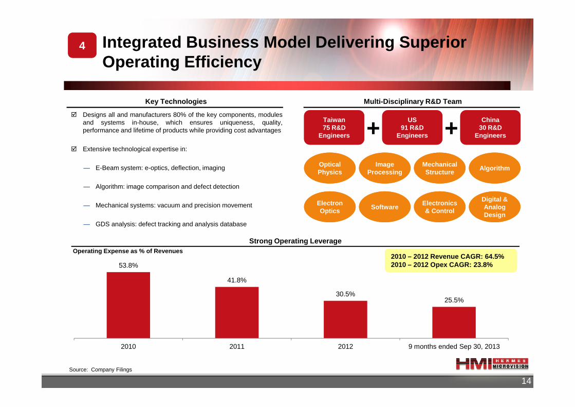
Key Technologies Multi-Disciplinary R&D Team
� Designs all and manufacturers 80% of the key components, modulesand systems in-house, which ensures uniqueness, quality,performance and lifetime of products while providing cost advantages
� Extensive technological expertise in:
— E-Beam system: e-optics, deflection, imaging
— Algorithm: image comparison and defect detection
— Mechanical systems: vacuum and precision movement
+Taiwan 75 R&D
Engineers
Taiwan 75 R&D
Engineers +US
91 R&D Engineers
US91 R&D
Engineers
China30 R&D
Engineers
China30 R&D
Engineers
Optical PhysicsOptical Physics
Image Processing
Image Processing
Mechanical Structure
Mechanical Structure
AlgorithmAlgorithm
Electron Electron SoftwareSoftware
Electronics Electronics Digital & Analog
Digital & Analog
4 Integrated Business Model Delivering Superior Operating Efficiency
14
— Mechanical systems: vacuum and precision movement
— GDS analysis: defect tracking and analysis database
Electron Optics
Electron Optics SoftwareSoftware
Electronics & Control
Electronics & Control Analog
DesignAnalog Design
Strong Operating Leverage
Source: Company Filings
Operating Expense as % of Revenues2010 – 2012 Revenue CAGR: 64.5%2010 – 2012 Opex CAGR: 23.8%53.8%
41.8%
30.5%25.5%
2010 2011 2012 9 months ended Sep 30, 2013
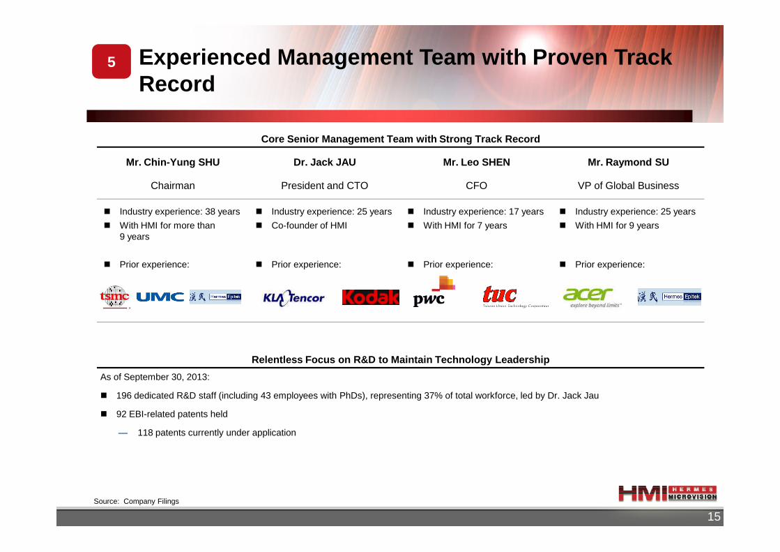
Mr. Chin-Yung SHU
Chairman
Dr. Jack JAU
President and CTO
Mr. Leo SHEN
CFO
Mr. Raymond SU
VP of Global Business
� Industry experience: 38 years
� With HMI for more than 9 years
� Prior experience:
� Industry experience: 25 years
� Co-founder of HMI
� Prior experience:
� Industry experience: 17 years
� With HMI for 7 years
� Prior experience:
� Industry experience: 25 years
� With HMI for 9 years
� Prior experience:
Core Senior Management Team with Strong Track Recor d
5 Experienced Management Team with Proven Track Record
15Source: Company Filings
As of September 30, 2013:
� 196 dedicated R&D staff (including 43 employees with PhDs), representing 37% of total workforce, led by Dr. Jack Jau
� 92 EBI-related patents held
— 118 patents currently under application
Relentless Focus on R&D to Maintain Technology Lead ership
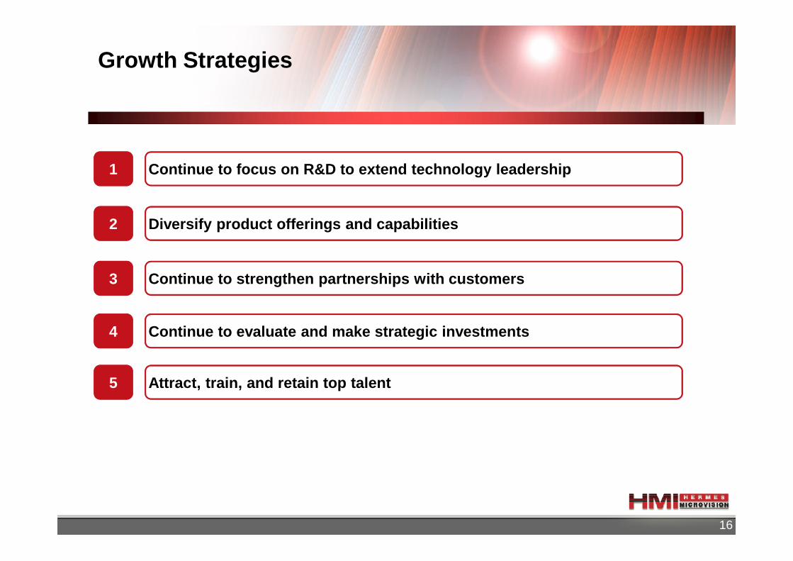
Growth Strategies
1 Continue to focus on R&D to extend technology leade rship
2 Diversify product offerings and capabilities
3 Continue to strengthen partnerships with customers
16
3 Continue to strengthen partnerships with customers
4 Continue to evaluate and make strategic investments
5 Attract, train, and retain top talent

III. Financial Highlights
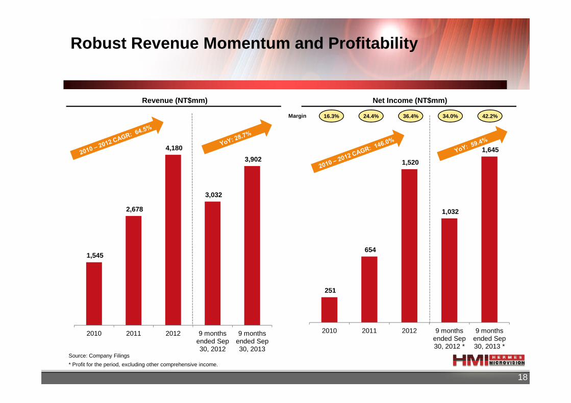
1,520
1,645 4,180
3,032
3,902
Robust Revenue Momentum and Profitability
Revenue (NT$mm) Net Income (NT$mm)
Margin 16.3% 24.4% 36.4% 34.0% 42.2%
18
251
654
1,032
2010 2011 2012 9 months ended Sep 30, 2012 *
9 months ended Sep 30, 2013 *
1,545
2,678
2010 2011 2012 9 months ended Sep 30, 2012
9 months ended Sep 30, 2013
Source: Company Filings
* Profit for the period, excluding other comprehensive income.
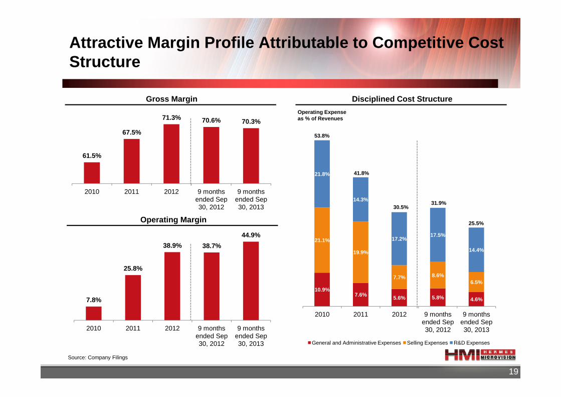
21.8%
14.3%
53.8%
41.8%
Attractive Margin Profile Attributable to Competiti ve Cost Structure
Disciplined Cost StructureGross Margin
Operating Expense as % of Revenues
61.5%
67.5%
71.3% 70.6% 70.3%
2010 2011 2012 9 months ended Sep
9 months ended Sep
19
10.9%7.6% 5.6% 5.8% 4.6%
21.1%
19.9%
7.7% 8.6%6.5%
14.3%
17.2%17.5%
14.4%
2010 2011 2012 9 months ended Sep 30, 2012
9 months ended Sep 30, 2013
General and Administrative Expenses Selling Expenses R&D Expenses
30.5%31.9%
25.5%Operating Margin
Source: Company Filings
ended Sep 30, 2012
ended Sep 30, 2013
7.8%
25.8%
38.9% 38.7%
44.9%
2010 2011 2012 9 months ended Sep 30, 2012
9 months ended Sep 30, 2013
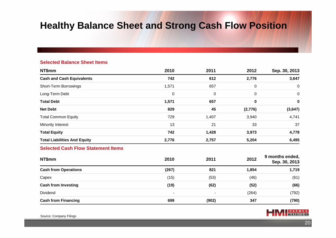
Healthy Balance Sheet and Strong Cash Flow Position
Selected Balance Sheet Items
NT$mm 2010 2011 2012 Sep. 30, 2013
Cash and Cash Equivalents 742 612 2,776 3,647
Short-Term Borrowings 1,571 657 0 0
Long-Term Debt 0 0 0 0
Total Debt 1,571 657 0 0
Net Debt 829 45 (2,776) (3,647)
Total Common Equity 729 1,407 3,940 4,741
20
Total Common Equity 729 1,407 3,940 4,741
Minority Interest 13 21 33 37
Total Equity 742 1,428 3,973 4,778
Total Liabilities And Equity 2,776 2,757 5,204 6,495
Selected Cash Flow Statement Items
NT$mm 2010 2011 20129 months ended,
Sep. 30, 2013
Cash from Operations (267) 821 1,854 1,719
Capex (15) (53) (46) (61)
Cash from Investing (19) (62) (52) (66)
Dividend - - (264) (792)
Cash from Financing 699 (902) 347 (790)
Source: Company Filings

APPENDIX
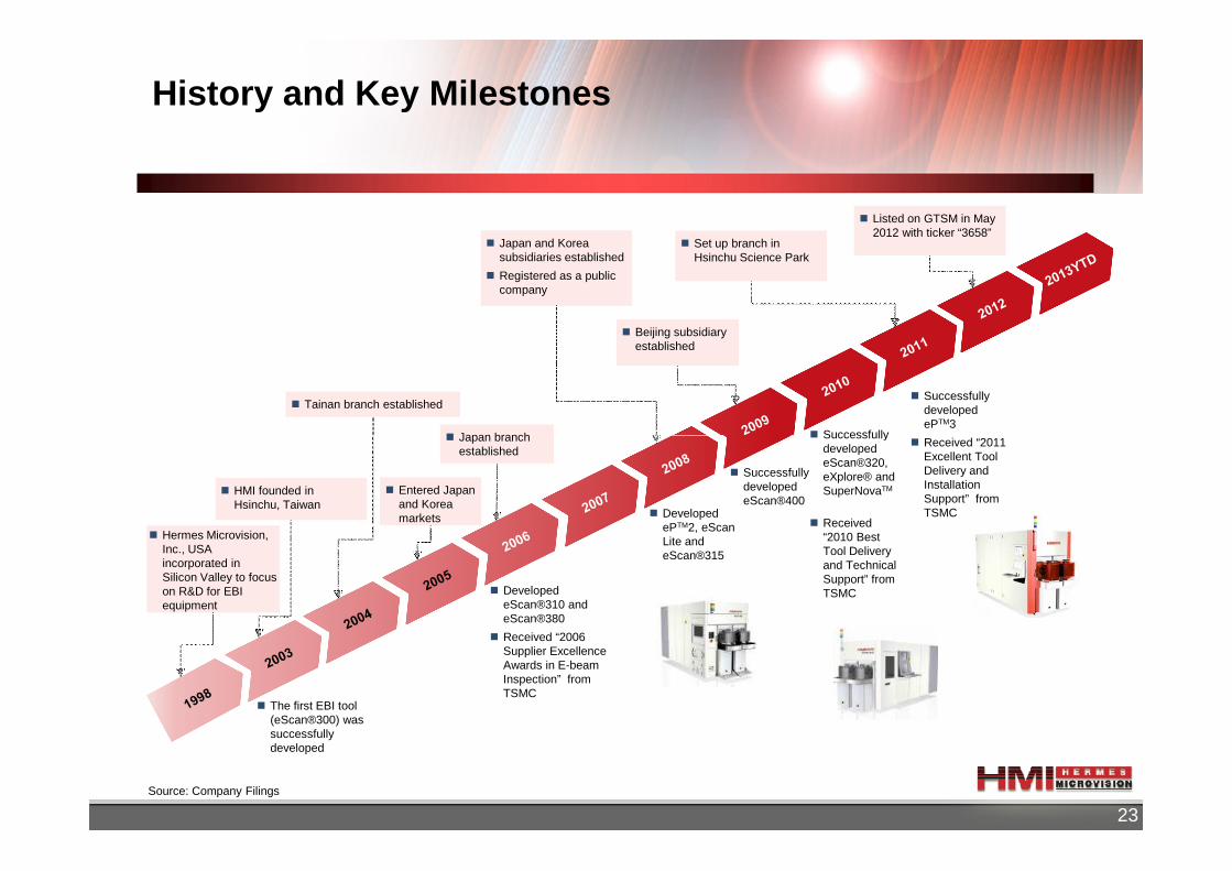
History and Key Milestones
2013 YTD� Tainan branch established
� Beijing subsidiary established
� Japan branch
� Japan and Korea subsidiaries established
� Registered as a public company
� Set up branch in Hsinchu Science Park
� Listed on GTSM in May 2012 with ticker “3658”
� Successfully
� Successfully developed ePTM3
23Source: Company Filings
19982003
20042005
2006
2007
2008
2009
2010
2012
� The first EBI tool (eScan®300) was successfully developed
� Hermes Microvision, Inc., USA incorporated in Silicon Valley to focus on R&D for EBI equipment
� HMI founded in Hsinchu, Taiwan
� Japan branch established
� Entered Japan and Korea markets
� Successfully developed eScan®320, eXplore® and SuperNovaTM
� Received “2010 Best Tool Delivery and Technical Support” from TSMC
� Developed ePTM2, eScan Lite and eScan®315
� Developed eScan®310 and eScan®380
� Received “2006 Supplier Excellence Awards in E-beam Inspection” from TSMC
� Successfully developed eScan®400
� Received “2011 Excellent Tool Delivery and Installation Support” from TSMC
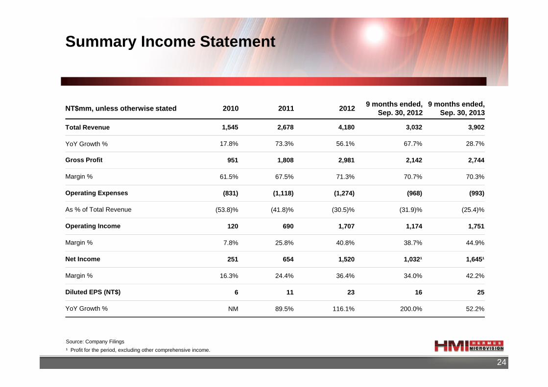
Summary Income Statement
NT$mm, unless otherwise stated 2010 2011 20129 months ended,
Sep. 30, 20129 months ended,
Sep. 30, 2013
Total Revenue 1,545 2,678 4,180 3,032 3,902
YoY Growth % 17.8% 73.3% 56.1% 67.7% 28.7%
Gross Profit 951 1,808 2,981 2,142 2,744
Margin % 61.5% 67.5% 71.3% 70.7% 70.3%
Operating Expenses (831) (1,118) (1,274) (968) (993)
24
Operating Expenses (831) (1,118) (1,274) (968) (993)
As % of Total Revenue (53.8)% (41.8)% (30.5)% (31.9)% (25.4)%
Operating Income 120 690 1,707 1,174 1,751
Margin % 7.8% 25.8% 40.8% 38.7% 44.9%
Net Income 251 654 1,520 1,032¹ 1,645¹
Margin % 16.3% 24.4% 36.4% 34.0% 42.2%
Diluted EPS (NT$) 6 11 23 16 25
YoY Growth % NM 89.5% 116.1% 200.0% 52.2%
Source: Company Filings
¹ Profit for the period, excluding other comprehensive income.
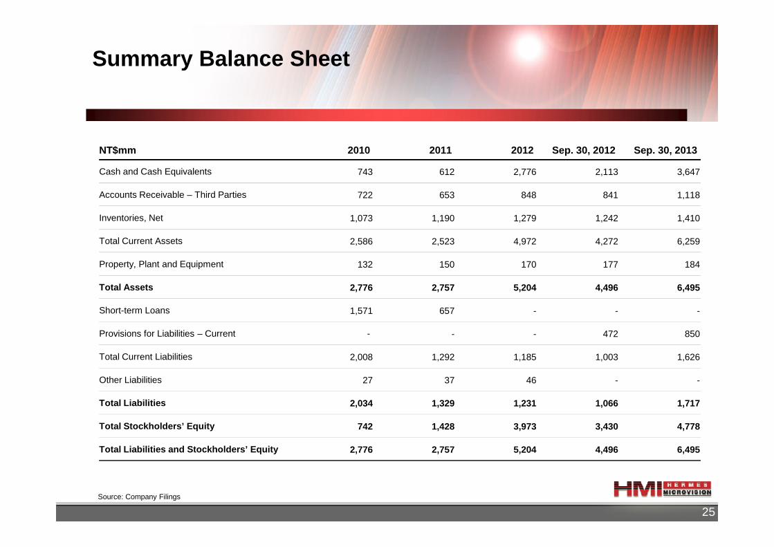
Summary Balance Sheet
NT$mm 2010 2011 2012 Sep. 30, 2012 Sep. 30, 2013
Cash and Cash Equivalents 743 612 2,776 2,113 3,647
Accounts Receivable – Third Parties 722 653 848 841 1,118
Inventories, Net 1,073 1,190 1,279 1,242 1,410
Total Current Assets 2,586 2,523 4,972 4,272 6,259
Property, Plant and Equipment 132 150 170 177 184
25
Total Assets 2,776 2,757 5,204 4,496 6,495
Short-term Loans 1,571 657 - - -
Provisions for Liabilities – Current - - - 472 850
Total Current Liabilities 2,008 1,292 1,185 1,003 1,626
Other Liabilities 27 37 46 - -
Total Liabilities 2,034 1,329 1,231 1,066 1,717
Total Stockholders’ Equity 742 1,428 3,973 3,430 4,778
Total Liabilities and Stockholders’ Equity 2,776 2,757 5,204 4,496 6,495
Source: Company Filings
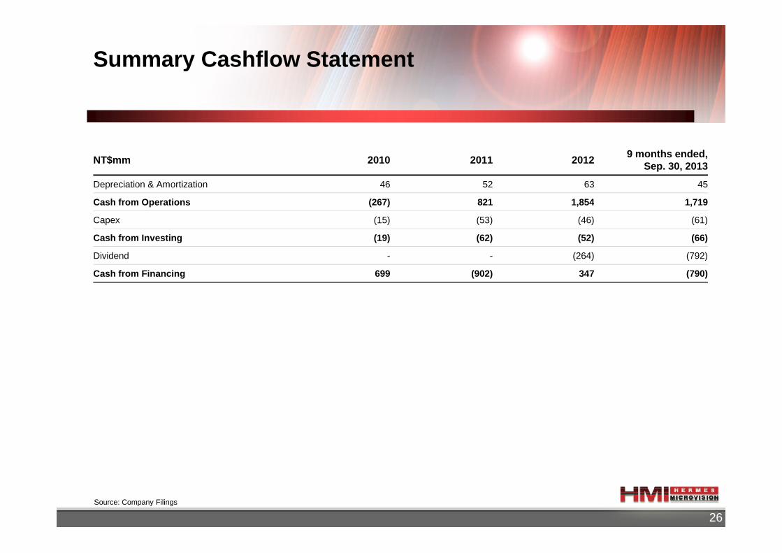
Summary Cashflow Statement
NT$mm 2010 2011 20129 months ended,
Sep. 30, 2013
Depreciation & Amortization 46 52 63 45
Cash from Operations (267) 821 1,854 1,719
Capex (15) (53) (46) (61)
Cash from Investing (19) (62) (52) (66)
Dividend - - (264) (792)
Cash from Financing 699 (902) 347 (790)
26
Cash from Financing 699 (902) 347 (790)
Source: Company Filings