Heterogeneous Integration of Enhancement Mode InO.7GaO.3As Quantum WellTransistor on Silicon Substrate using Thin (< 2 gim) Composite Buffer Architecture
for High-Speed and Low-voltage ( 0.5V) Logic Applications
M. K. Hudait, G. Dewey, S. Datta, J. M. Fastenau*, J. Kavalieros, W. K. Liu*, D. Lubyshev*,R. Pillarisetty, W. Rachmady, M. Radosavljevic, T. Rakshit and Robert Chau
Technology and Manufacturing Group, Intel Corporation, Hillsboro, OR-97124, USA*IQE Inc, Bethlehem, USA
Contact: robert.s.chau(inte1 cor
Abstract were evaluated using high-resolution x-ray rocking curve, asThis paper describes for the first time, the heterogeneous shown in Fig. 3. The angular separation between the
integration of InO.7Ga0.3As quantum well device structure on diffraction peaks of GaAs with respect to Si confirms fullSi substrate through a novel, thin composite metamorphic relaxation of the GaAs layer. The indium composition of thebuffer architecture with the total composite buffer thickness InxAll-xAs buffer layer is graded from 0 to 52%, with ansuccessfully scaled down to 1.3gm, resulting in high- overshoot of indium concentration (0.52<x<0.7) in-between,performance short-channel enhancement-mode InO7Ga03As as evidenced by the two peaks existing in the InxAlj_xAsQWFETs on Si substrate for future high-speed digital logic buffer region of Fig. 3. This overshoot was employed toapplications at low supply voltage such as 0.5V. ensure full relaxation of this buffer layer while minimizing its
total thickness. The relaxation of the entire composite bufferIntroduction layer allows the growth of a defect-free 1no.7Ga0.3As QW on
The InGaAs quantum well field effect transistor Si (Figs.2a-2c). Figs. 2c and 3 suggest the InO.7Ga0.3As QW(QWFET) is one of the most promising device candidates for layer is compressively strained with respect to thefuture high-speed and low-power digital logic applications In0.52A10.48As barrier. AFM surface morphology of thedue to high electron mobility, large F to L valley separation 1nO.7Ga0.3As QW layers grown on Si with 2tm and 1.3tmand good short-channel performance [1-3]. A seamless, composite buffers exhibit a cross-hatch pattern, as shown inrobust heterogeneous integration of high-performance Figs. 4a and 4b respectively, demonstrating excellentInGaAs QWFET on Si substrate will allow low-voltage, metamorphic growth of the buffer layers. The surface rmshigh-speed Ill-V based logic circuit blocks to couple with the roughness of Ino.7Ga0.3As QW grown on Si was measuredmain stream Si CMOS platform for future microprocessor over an area of 5x5gm2 to be less than 4nm, which is similarapplications, while avoiding the need for developing large to that of Ino.7Ga0.3As QW grown on GaAs [4].diameter (>300mm) Ill-V substrates. This paper describes in Figure 5a shows the 1nO.7Ga0.3As QW mobility at 300Kdetail for the first time, the integration of InO.7Ga0.3As and 77K as a function of total buffer thickness ranging fromquantum well (QW) structure on Si through a novel, thin 3.2gm to 1.3gm of the composite buffer grown on Si. Nocomposite metamorphic buffer architecture consisting of mobility degradation is observed for all the bufferGaAs and graded 1nxAlj_xAs layers, resulting in short-channel thicknesses, demonstrating that the thin compositeenhancement-mode 1nO.7Ga0.3As QWFETs on silicon with metamorphic buffer architecture is effective in filteringhigh performance at low supply voltage of 0.5V. dislocations. Fig. 5b compares the Hall mobility versus sheet
carrier density (Ns) measured in the InO.7Ga0.3As QW layersMaterials Growth and Characterization grown on Si, GaAs and InP substrates at 300K and 77K. For
Ino.7Ga0.3As quantum well (QW) device layers shown in a given Ns, the mobility in the InO 7Ga0 3As QW layer grownFig. 1 were heterogeneously grown on 40 off-cut (100) p-type on silicon via the composite buffer is equivalent to those inSi substrates with lattice mismatch of>8% using a composite the InO 7Ga0O3As QW layers grown on Ill-V substrates such asmetamorphic buffer consisting of GaAs and graded GaAs and InP. No degradation in QW mobility on Si isInxAll-xAs layers by solid source MBE. The thickness of the observed despite the >8% lattice mismatch, demonstratingcomposite buffer is successfully scaled down to 1.3gm for effective dislocation filtering using the composite buffer onthe first time without degrading the properties of Ino.7Ga0.3As Si. Fig. 6a shows the quantitative mobility spectrum analysisQW. Figs. 2a-2b show cross-sectional TEM images of the (QMSA) for 1nO.7Ga0.3As QW on Si at different temperatures.entire structure grown on Si with 1.5gm and 1.3gm The large conductivity ratio between the majority carriercomposite buffer, respectively. In both cases, the misfit and (electrons) and the minority carrier (holes) at all temperaturesthreading dislocations are predominantly contained in the and also the increase in electron mobility with decreasingcomposite buffer, and the active device layers are virtually temperature suggest no parallel, parasitic conduction in Si ordefect-free, which is also shown in Fig. 2c using high- through the composite buffer layer. In addition, both Ns andresolution TEM. The relaxation state and the grading scheme mobility exhibit no dependence on magnetic field at different
temperatures, as shown in Fig. 6b, further indicating no Referencesparallel, parasitic conduction in the buffer layer or in Si. [1]S. Datta et al, IEEE Electron Dev. Lett., vol. 28 (8), p. 685 (2007).
[2]D. Kim and J. A. del Alamo, IEDM Tech. Dig., p. 837 (2006).Device Characteristics [3]Y. Yamashita et al, IEEE Electron Dev. Lett., vol. 23 (10), p. 573 (2002).
[4]D. Lubyshev et al, J. Vac. Sci. Technol. B, vol. 22 (3), p. 1565 (2004).Figure 7 shows the SEM micrograph of an 1no7Gao3As
QWFET on Si with the composite buffer described above. n+4n053Ga047Ascontact .20 nmThe use of a combination of wet and RIB etch to recess the .etch stop 6 nmgate towards the channel, as well as Pt/Au Schottky gates, InA eA tb r 8enable enhancement-mode (e-mode) operation and improve t baffier gnm
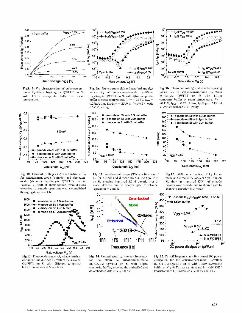
short channel performance of the device. The ID-VDScharacteristics of the e-mode LG=80nm InO.7GaO.3As QWFET In0!!A18As sae layer 5 !nm!on Si with 1.3gm composite buffer layer iS shown in Fig. 8. Ip0G Asch el :1 nFigs. 9a and 9b show the ID-VG characteristics of the e-mode In05210||1 |48As |bottom bare :10 nm 2LG=80nm 1n0.7Ga0.3As QWFETs on Si with 2gm and 1.3gm gradedllilb ilullffer(x0-0.52): 0.7-1.1llllllIIIIIIIIm II lbuffer, respectively. The Schottky gate leakage iS also oincluded for reference. Both devices exhibit good transistor GaA nulainad ufrlyr:0520pcharacteristics and high performance at VDS=O.SV. TheJSLG=80nm 1n07Ga0.3As QWrET on Si with 1.3gm composite 4010 Offeuti p-typ Si subsratcbuffer achieves threshold voltage (VT)= ± 0.1 1V, 'Dsat=0.32mA/gm and 'ON"IOFF =2150 at VDS=O.SV with 0.5V VG Fig.1: Heterogeneous integration of Ino7Gao3As QWFETs on Si using
, , , ~~~~~~metamorphic composite buffer architecture consisting of GaAs andswing. Fig. 10 shows VT as a function of LG for the e-modle InxAli xAs graded buffer layers. The composite buffer in this work hasand depletion-mode (d-mode) 1n0.7Ga0.3As QWFETs on Si. A total thickness in the range oft1.3,um to 3.2,um.positive VT shift of ~600mV from d-mode to e-mode
11 and 12 show the sub-threshold slope (SS) anld drain n7a3 Qinduced barrier lowering (DIBL), respectively as a function
wimprovedSS and DIB of e-od over d-oe deicessaVD=0.iV
Fig. 13 shows the turancndutgainc(Gl) chausraeristicsofth e-mode aG8nd-mod LOGaO QWFETIn nGaASiQwFEts on3RSi .2:CosscinlTMiag fIO7a WE nSwihdftcomposite bufferthVS=.V ickne5sse wsathVDS of usnl5ucopstbfer5Viftndhedndslctosr
1.5gmqufferlayer ovefn thatof the e-modedevsiceiocoprn rdmnnl otie ntecmoiebfe,with 2gmIO7GO.
modee-oeLG =80nm In07Ga03As QWFET on Si with 1.3gm Fig 2ita:lCros-ectionlreMe mg.fIn7a3sQWE nS
composite buffer at VDS=O.5V versus the standard LG=60nmIn G0AsQSi n-MOSFET transistor at both VDS=0.5V and 1.1V. - &g_CoinetannorphicbufferamtottheuSi n-the e-modeInff GAhickessQWFETon Si exhb13mcomposits >1ffOX laere isson inDC powr bfG
speed perorance9fhor the sameG powaer. siso h -oeNgmbt6 hid 0im ;:
IG=80n0 IGanAs quantumQWEl stu Sr sha bendsuccessfully
metamorphicbuffer,respectivel. achi re wothy totale r thic sso
SInxluxsingrddbfelarsThcomposite bufferwihnotlthiknsso 1.3gm The s
and deletio-mode(d-moe) hI.7Gao3As QNTETson Si A toac thivkesIoGas QWteagis vir~tual deet-fre.2m
positive VT shift of -6OOmV from d-mode to e-modeIn GaA626
Authorized licensed use limited to: Penn State University. Downloaded on November 13, 2009 at 23:55 from IEEE Xplore. Restrictions apply.
Gao.47As l~~~nxAll_xAs graded buffer Si substrateXX GaAs buffer
nP~~ ~ ~ ~~ mg etc st csec
32gm
0)~~~~~~~~~~~~~~~~~~~~~~~~~25
I5gm
Fig. 2c: High-resolution TEM of In0 7Gao 3As Fig. 3: High-resolution x-ray rocking curves from Fig. 4a: AFM image from the surface ofQW, In0 52A10G48As barriers, InP etch stop and the (004) Bragg lines of In 7Gao 3As QWFET Ino7Gao3As QW layer on Si with 2,umIno53Ga047As cap layer. The device layers are structures on Si substrates with different composite composite buffer shows cross-hatch patterndefect-free. buffer thicknesses ranging from 1.3-3.2,um. with surface rms roughness of 30A.
40 i _ X - _ On Si * 300K : 77K
1.3rm~~ ~ ~ ~ 0bufe== OnG00AsI300K;7300
In,,A~ s bttoa 0W A
E1000000
0 Zb5U 5. 1.2 1 .. .428 Omga2tht [arcsec]4xo2 ... x1Fig. 2c: AFMigh-resoluton theM srfofln7Go3_ Fig.5a: High-resolto x-raelcrockn gcurltyverssfrm Fig. 4a:Eletro im ageitversus thee sufcarer denitQWInao.52As0QWA barrersIn Peiwtch stop,um copsthe bufferaglayrticnessof noSiGao.3A_s QWFE l n .7Ga0.3A_s QWlayer on Si (vith novel
withosurfaoe47As capoughn Tes deic layer aremostructursing Sia susrthes witamrhdifentcopst cmoiebufferans7.hodgrdtowsi crsshacmobiltyeonSdefect-free. buff~~~~achietretickessraetienfiteingfr som ca32tion. desith 8sur ace ticeroghesmaof mostr0in
E OAV ~~~~~EA/-A _A_A0.20 E F-015 0.3V ~~~~~~~~~~~=-~ 103 /=I-10-0 A~~~~~~~~~~~~~~~~~~~~~~~~~~kA
.E0.10 )kA!
0.05 0. 06 /A -A-LGI)S=.5 106 AA-A' (VDAOO5
0.00 ~~~~~0.IV - 2gm buffer -A
G (~VDS=O.5V 71.3gm buffer G (~VDS=O.5V0.0 0.1 0.2 0.3 0.4 0.5 10 u 10-0.0 0.10.2 0.3 0.4 0.5 -0.4 -0.2 0.0 0.2 0.4 0.6 -0.4 -0.2 0.0 0.2 0.4 0.6Danvoltage, VDS M Gate voltage, VG [V Gate voltage, VG [MI
Fig.8: ID-VDS characteristics of enhancement- Fig. 9a: Drain current (ID) and gate leakage (IG) Fig. 9b: Drain current (ID) and gate leakage (IG)mode LG""8Onm In0 7GaO.3As QWFET on Si versus VG of enhancement-mode LG""8Onm versus VG of enhancement-mode LG""8Onmwith 1.3gtm composite buffer at room InO.7GaO.3As QWFET on Si with 2gtm composite InO.7GaO.3As QWFET on Si with 1.3gtmtemperature. buffer at room temperature. VT"" ± 0.07V, IDsat= composite buffer at room temperature. VT=
0.25mA/gtm, ION/JOFF =2500 at VDs=0O.5V with ±0.11IV, IDsat =0.32mnA/gtm, ION/JOFF =2150 at0.5V VG swing. VDs=0O.5V with 0.5V VG swing.
> 0.2 200 22CLO ~ ~__*-U- e-mode on Si with 1.3gm buffer- -emdonSwih13mbfr
) u 180 -*-- e-mode on Si with 2gm buffer20 --em eonSwih13mbfrC', 0.0 -*-d-mode~~~~~~~a)-4---e-mode on Si with 2gm buffer
cn 0.0 --0-d-mode on ~~~~~Si with 2gm buffer 180 *--d-mode on Si with 2gm bufferE 160 -160
600mV 140
0140 @ 20~~~~~~~~~~~~~~~~~~~~~~~~~
v-0.6 -10 U~6o -m- e-mode on Si with 1.3gm buffer In40-08~ e-mode on Si with 2gm buffer 80 -20 VSOS
.~ -4- d-mode on Si with 2gm buffer. I . I . ~60 ' ' ' ' ' I
Gate length, LG [nm] Gate length, LG [nm] Gate length, LG [nm]
Fig. 10: Threshold voltage (VT) as a function of LG Fig. 11: Sub-threshold slope (SS) as a function of Fig.12: DIBL as a function of LG for e-for enhancement-mode (e-mode) and depletion- LG for e-mode and d-mode In0 7GaO.3As QWFETs mode and d-mode In0 7GaO.3As QWFETs onmode (d-mode) Ino.7GaO.3As QWFETs on Si. on Si, showing improved SS of e-mode over d- Si, showing improved DIBL of e-modePositive VT shift of about 600mV from d-mode mode devices due to shorter gate to channel devices over d-mode due to shorter gate tooperation to e-mode operation was accomplished separation in e-mode. channel separation in e-mode.through gate recess etch. 50- 450
De-erAxxkled -y-- e-mode In0 7Ga0 3As QWFET on Si1800
Gate voltage, VG [IV]Fig.13: Transconductance, G. characteristics Fig. 14: Current gain (h2l) versus frequency Fig. 15: Cut-off frequency as a function ofDC powerof e-mode and d-mode LG ""8Onm InO.7GaO.3As for the 8Onm LG enhancement-mode dissipation for the enhancement-mode LG""8OnmQWFTsPT on Si; wAith di-FFerent onmposite n7GoA QWAAUF on Si; w It '21.3g InoGa3As Q F on Si wIt1.g copse
Authorized licensed use limited to: Penn State University. Downloaded on November 13, 2009 at 23:55 from IEEE Xplore. Restrictions apply.