7
HETEROJUNCTION TECHNOLOGY THE SOLAR CELL OF THE FUTURE
HETEROJUNCTIONTECHNOLOGYTHE SOLAR CELL
OF THE FUTURE

2 3
ABSTRACT
Wafer-based silicon photovoltaic (PV) production has only changed slightly in the last forty years. The standard concept comprises p-type silicon wafers, fired contacts and encapsulation. Cost reduction is necessary if PV is to survive without feed-in tariffs and be competitive with grid electricity costs. Therefore levelised cost of electricity (LCOE) is one of the primary metrics for the cost of electricity produced by both utility scale and distributed power systems. The fastest path to lower LCOE is to introduce high efficiency solar cell concepts like the heterojunction technology (HJT). Photovoltaic systems using heterojunction technology (HJT) modules outperform any other PV systems and this paper will explain why.
Introduction
Meyer Burger develops solar technology – from wafers to com-plete PV systems – with the aim of promoting the widespread use of photovoltaics and making solar power a first-choice source of renewable energy. To this end, the company focuses strongly on developing solar cell technologies which allows highest efficiencies and highest energy output at lowest production costs.
Heterojunction cell technology combines the advantages of mono crystalline silicon (c-Si) solar cells with the good absorption and the superior passivation characteristics of amorphous silicon (a-Si) known from a-Si thin film technology using readily available ma-terials. The HJT design is not new. Sanyo (now Panasonic) first pushed this technology into mass production achieving around 20% cell efficiency.
Recently Panasonic demonstrated efficiencies of 24.7% on laboratory scale cells [1]. With the discontinuation of the basic technology patent, heterojunction technology was opened to the public in 2010. Meyer Burger is now offering this appealing technology as a high performance key technology in the photovoltaic value chain.
The simple structure of a HJT cell is shown in Figure 1. The thin intrinsic a-Si:H layers deposited between c-Si wafer and doped layers are key to achieving maximum performance from the cell structure. They result in reduced interface state density, decreased surface recombination losses and lower the emitter saturation currents.
HETEROJUNCTION TECHNOLOGY
Figure 1:Schematic drawing of the HJT cell and the process steps required
Ag (screen print)
ITO
(p) a-Si:H
(i) a-Si:H
(i) a-Si:H
(n) a-Si:HITO
Ag (PVD)
n-type c-Si
Texture
a-Si Front / Rear Side
TCO / Metal Rear Contact
Print Front Side
Curing
Test & Sort
G. Roters1, J. Krause1, S. Leu2, A. Richter2, B. Strahm3
1 Roth & Rau AG, An der Baumschule 6-8, 09337 Hohenstein-Ernstthal, Germany 2 Meyer Burger Technology Ltd, Schorenstrasse 39, CH-3645 Gwatt (Thun), Switzerland 3 Roth & Rau Research AG, Rouges-Terres 61, CH-2068 Hauterive, Switzerland
CZ: 19%MC: 16.8 – 17.5%
CZ: 19 – 20%MC: 18 – 19%
CZ: 20 – 21%MC: 18 – 19%
CZ n-type: 21 ~ 25%
Texture
Doping / Diffusion
Edge Isolation
PSG Etch
AR Coating
Print Rear Side
Print Front Side
Firing
Test & Sort
Standard process
Texture
Doping / Diffusion
Additional 4 Process Steps
Edge Isolation
PSG Etch
AR Coating
Print Front Side
Print Rear Side
Firing
Test & Sort
Sel. Emitter process
Laser Drilling
Texture
Doping / Diffusion
PSG Etch
AR Coating
Print Front Gridand p-Contact
Firing
Edge Isolation (Front)
Edge Isolation (Rear)
Test & Sort
MWT process
Texture
a-Si Front / Rear Side
TCO / Metal Rear Contact
Print Front Side
Curing
Test & Sort
Significantpotential forcost savings!
HJT process
The relatively straightforward HJT production process takes place at low temperatures and requires fewer production steps compared to other high efficiency designs as shown in Figure 2, which is eco-nomically attractive as it results in significant energy cost savings.
An important technological advantage of HJT cells is the excellent surface passivation of a-Si:H which results in high open-circuit volt-ages and high cell efficiencies. The superior temperature coefficient of TC = -0.20%/K ensures higher energy yield during module op-erating conditions. As previously mentioned, low temperature pro-cessing (<250°C) saves energy during manufacturing, prevents bulk degradation and enables the use of thin wafers. Integrated develop-ment throughout the PV value chain (diamond wire wafering, het-erojunction cell technology and SmartWire Connection Technology (SWCT) guarantees the maximum performance of HJT modules.
Meyer Burger technology for high performance solutions ensures the perfect integration and harmonisation of all processes with the goal of lowest LCOE.
Thin wafers
Today, wafers with a thickness of ~180 µm are in standard use in cell manufacturing. A wafer thick-ness even below 100 µm is enough for absorb-ing light in silicon solar cells. Using thinner wafers leads to significantly lower material costs because a higher number of wafers can be cut from one brick. With decreasing wafer thickness, the influ-ence of the bulk material quality also decreases resulting in less tight requirements for e.g. minor-ity charge carrier lifetimes. Diamond wire sawing is the best approach for thin wafers. The use of diamond wire leads to fewer microcracks and the depth of microcracks is shallower. With decreas-ing wafer thickness and the corresponding higher surface to bulk ratio the surface recombination loss becomes dominant compared to recombi-nation loss in the bulk. Consequently superior surface passivation techniques are mandatory.
Figure 2:Process sequence of differing PV technologies
Texture
Doping / Diffusion
Edge Isolation
PSG Etch
SiNx Capping- & AlOx passivation-layer
AR Coating
Laser contact opening
Print Front- & Rear-side
Firing
Test & Sort
MB-PERC
CZ: 20 – 21%MC: 19 – 20%
mean cell thickness [µm]
cell
effic
ienc
y [%
]80 100 120 140 160 180 200 220 240 260
25.0
24.0
23.0
22.0
21.0
20.0
4 5
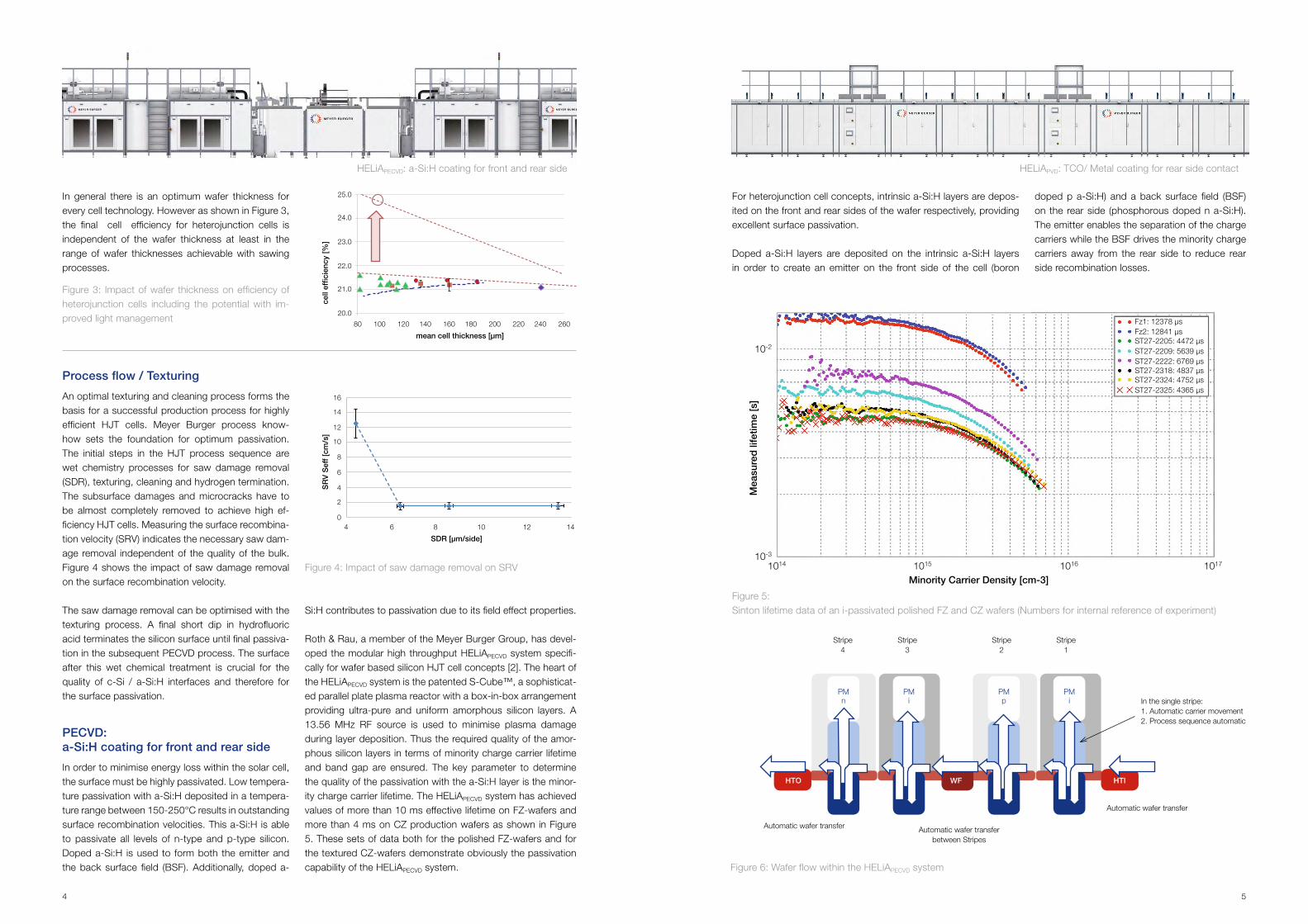
In general there is an optimum wafer thickness for every cell technology. However as shown in Figure 3, the final cell efficiency for heterojunction cells is independent of the wafer thickness at least in the range of wafer thicknesses achievable with sawing processes.
Figure 3: Impact of wafer thickness on efficiency of heterojunction cells including the potential with im-proved light management
For heterojunction cell concepts, intrinsic a-Si:H layers are depos-ited on the front and rear sides of the wafer respectively, providing excellent surface passivation.
Doped a-Si:H layers are deposited on the intrinsic a-Si:H layers in order to create an emitter on the front side of the cell (boron
doped p a-Si:H) and a back surface field (BSF) on the rear side (phosphorous doped n a-Si:H). The emitter enables the separation of the charge carriers while the BSF drives the minority charge carriers away from the rear side to reduce rear side recombination losses.
SDR [µm/side]
SR
V S
eff
[cm
/s]
4 6 8 10 12 14
16
14
12
10
8
6
4
2
0
Process flow / Texturing
An optimal texturing and cleaning process forms the basis for a successful production process for highly efficient HJT cells. Meyer Burger process know-how sets the foundation for optimum passivation. The initial steps in the HJT process sequence are wet chemistry processes for saw damage removal (SDR), texturing, cleaning and hydrogen termination. The subsurface damages and microcracks have to be almost completely removed to achieve high ef-ficiency HJT cells. Measuring the surface recombina-tion velocity (SRV) indicates the necessary saw dam-age removal independent of the quality of the bulk. Figure 4 shows the impact of saw damage removal on the surface recombination velocity.
The saw damage removal can be optimised with the texturing process. A final short dip in hydrofluoric acid terminates the silicon surface until final passiva-tion in the subsequent PECVD process. The surface after this wet chemical treatment is crucial for the quality of c-Si / a-Si:H interfaces and therefore for the surface passivation.
PECVD: a-Si:H coating for front and rear side
In order to minimise energy loss within the solar cell, the surface must be highly passivated. Low tempera-ture passivation with a-Si:H deposited in a tempera-ture range between 150-250°C results in outstanding surface recombination velocities. This a-Si:H is able to passivate all levels of n-type and p-type silicon. Doped a-Si:H is used to form both the emitter and the back surface field (BSF). Additionally, doped a-
Si:H contributes to passivation due to its field effect properties.
Roth & Rau, a member of the Meyer Burger Group, has devel-oped the modular high throughput HELiAPECVD system specifi-cally for wafer based silicon HJT cell concepts [2]. The heart of the HELiAPECVD system is the patented S-Cube™, a sophisticat-ed parallel plate plasma reactor with a box-in-box arrangement providing ultra-pure and uniform amorphous silicon layers. A 13.56 MHz RF source is used to minimise plasma damage during layer deposition. Thus the required quality of the amor-phous silicon layers in terms of minority charge carrier lifetime and band gap are ensured. The key parameter to determine the quality of the passivation with the a-Si:H layer is the minor-ity charge carrier lifetime. The HELiAPECVD system has achieved values of more than 10 ms effective lifetime on FZ-wafers and more than 4 ms on CZ production wafers as shown in Figure 5. These sets of data both for the polished FZ-wafers and for the textured CZ-wafers demonstrate obviously the passivation capability of the HELiAPECVD system.
Figure 4: Impact of saw damage removal on SRVMinority Carrier Density [cm-3]
Mea
sure
d li
fetim
e [s
]
10-2
10-3
1014 1015 1016 1017
Fz1: 12378 µsFz2: 12841 µsST27-2205: 4472 µsST27-2209: 5639 µsST27-2222: 6769 µsST27-2318: 4837 µsST27-2324: 4752 µsST27-2325: 4365 µs
In the single stripe:1. Automatic carrier movement2. Process sequence automatic
Stripe 4
Stripe 3
Stripe 2
Stripe 1
Automatic wafer transfer Automatic wafer transferbetween Stripes
Automatic wafer transfer
PMn
PMi
PMp
PMi
HTO WF HTI
Figure 5:Sinton lifetime data of an i-passivated polished FZ and CZ wafers (Numbers for internal reference of experiment)
Figure 6: Wafer flow within the HELiAPECVD system
HELiAPECVD: a-Si:H coating for front and rear side HELiAPVD: TCO/ Metal coating for rear side contact
A - Load
B - Process
C - Process
D - Unload
CALiPSO: flexible heat treatment furnace
Figure 9:Measuring methodology of the newPasan spotLIGHT HighCap [3]
6 7
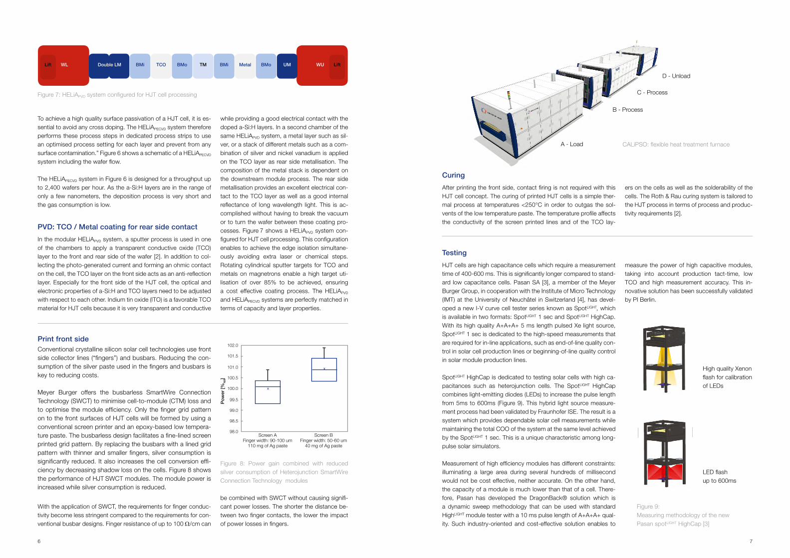
To achieve a high quality surface passivation of a HJT cell, it is es-sential to avoid any cross doping. The HELiAPECVD system therefore performs these process steps in dedicated process strips to use an optimised process setting for each layer and prevent from any surface contamination.” Figure 6 shows a schematic of a HELiAPECVD system including the wafer flow.
The HELiAPECVD system in Figure 6 is designed for a throughput up to 2,400 wafers per hour. As the a-Si:H layers are in the range of only a few nanometers, the deposition process is very short and the gas consumption is low.
PVD: TCO / Metal coating for rear side contact
In the modular HELiAPVD system, a sputter process is used in one of the chambers to apply a transparent conductive oxide (TCO) layer to the front and rear side of the wafer [2]. In addition to col-lecting the photo-generated current and forming an ohmic contact on the cell, the TCO layer on the front side acts as an anti-reflection layer. Especially for the front side of the HJT cell, the optical and electronic properties of a-Si:H and TCO layers need to be adjusted with respect to each other. Indium tin oxide (ITO) is a favorable TCO material for HJT cells because it is very transparent and conductive
while providing a good electrical contact with the doped a-Si:H layers. In a second chamber of the same HELiAPVD system, a metal layer such as sil-ver, or a stack of different metals such as a com-bination of silver and nickel vanadium is applied on the TCO layer as rear side metallisation. The composition of the metal stack is dependent on the downstream module process. The rear side metallisation provides an excellent electrical con-tact to the TCO layer as well as a good internal reflectance of long wavelength light. This is ac-complished without having to break the vacuum or to turn the wafer between these coating pro-cesses. Figure 7 shows a HELiAPVD system con-figured for HJT cell processing. This configuration enables to achieve the edge isolation simultane-ously avoiding extra laser or chemical steps. Rotating cylindrical sputter targets for TCO and metals on magnetrons enable a high target uti-lisation of over 85% to be achieved, ensuring a cost effective coating process. The HELiAPVD and HELiAPECVD systems are perfectly matched in terms of capacity and layer properties.
Print front sideConventional crystalline silicon solar cell technologies use front side collector lines (“fingers”) and busbars. Reducing the con-sumption of the silver paste used in the fingers and busbars is key to reducing costs.
Meyer Burger offers the busbarless SmartWire Connection Technology (SWCT) to minimise cell-to-module (CTM) loss and to optimise the module efficiency. Only the finger grid pattern on to the front surfaces of HJT cells will be formed by using a conventional screen printer and an epoxy-based low tempera-ture paste. The busbarless design facilitates a fine-lined screen printed grid pattern. By replacing the busbars with a lined grid pattern with thinner and smaller fingers, silver consumption is significantly reduced. It also increases the cell conversion effi-ciency by decreasing shadow loss on the cells. Figure 8 shows the performance of HJT SWCT modules. The module power is increased while silver consumption is reduced.
With the application of SWCT, the requirements for finger conduc-tivity become less stringent compared to the requirements for con-ventional busbar designs. Finger resistance of up to 100 Ω/cm can
Po
wer
[%re
l]
Screen AFinger width: 90-100 um
110 mg of Ag paste
102.0
101.5
101.0
100.5
100.0
99.5
99.0
98.5
98.0Screen B
Finger width: 50-60 um40 mg of Ag paste
Figure 8: Power gain combined with reduced silver consumption of Heterojunction SmartWire Connection Technology modules
WL UMLift Double LM WU LiftBMi TCO BMo TM BMi Metal BMo
Figure 7: HELiAPVD system configured for HJT cell processing
be combined with SWCT without causing signifi-cant power losses. The shorter the distance be-tween two finger contacts, the lower the impact of power losses in fingers.
Curing
After printing the front side, contact firing is not required with this HJT cell concept. The curing of printed HJT cells is a simple ther-mal process at temperatures <250°C in order to outgas the sol-vents of the low temperature paste. The temperature profile affects the conductivity of the screen printed lines and of the TCO lay-
High quality Xenon flash for calibration of LEDs
LED flash up to 600ms
ers on the cells as well as the solderability of the cells. The Roth & Rau curing system is tailored to the HJT process in terms of process and produc-tivity requirements [2].
Testing
HJT cells are high capacitance cells which require a measurement time of 400-600 ms. This is significantly longer compared to stand-ard low capacitance cells. Pasan SA [3], a member of the Meyer Burger Group, in cooperation with the Institute of Micro Technology (IMT) at the University of Neuchâtel in Switzerland [4], has devel-oped a new I-V curve cell tester series known as SpotLIGHT, which is available in two formats: SpotLIGHT 1 sec and SpotLIGHT HighCap. With its high quality A+A+A+ 5 ms length pulsed Xe light source, SpotLIGHT 1 sec is dedicated to the high-speed measurements that are required for in-line applications, such as end-of-line quality con-trol in solar cell production lines or beginning-of-line quality control in solar module production lines.
SpotLIGHT HighCap is dedicated to testing solar cells with high ca-pacitances such as heterojunction cells. The SpotLIGHT HighCap combines light-emitting diodes (LEDs) to increase the pulse length from 5ms to 600ms (Figure 9). This hybrid light source measure-ment process had been validated by Fraunhofer ISE. The result is a system which provides dependable solar cell measurements while maintaining the total COO of the system at the same level achieved by the SpotLIGHT 1 sec. This is a unique characteristic among long-pulse solar simulators.
Measurement of high efficiency modules has different constraints: illuminating a large area during several hundreds of millisecond would not be cost effective, neither accurate. On the other hand, the capacity of a module is much lower than that of a cell. There-fore, Pasan has developed the DragonBack® solution which is a dynamic sweep methodology that can be used with standard HighLIGHT module tester with a 10 ms pulse length of A+A+A+ qual-ity. Such industry-oriented and cost-effective solution enables to
measure the power of high capacitive modules, taking into account production tact-time, low TCO and high measurement accuracy. This in-novative solution has been successfully validated by PI Berlin.
8 9
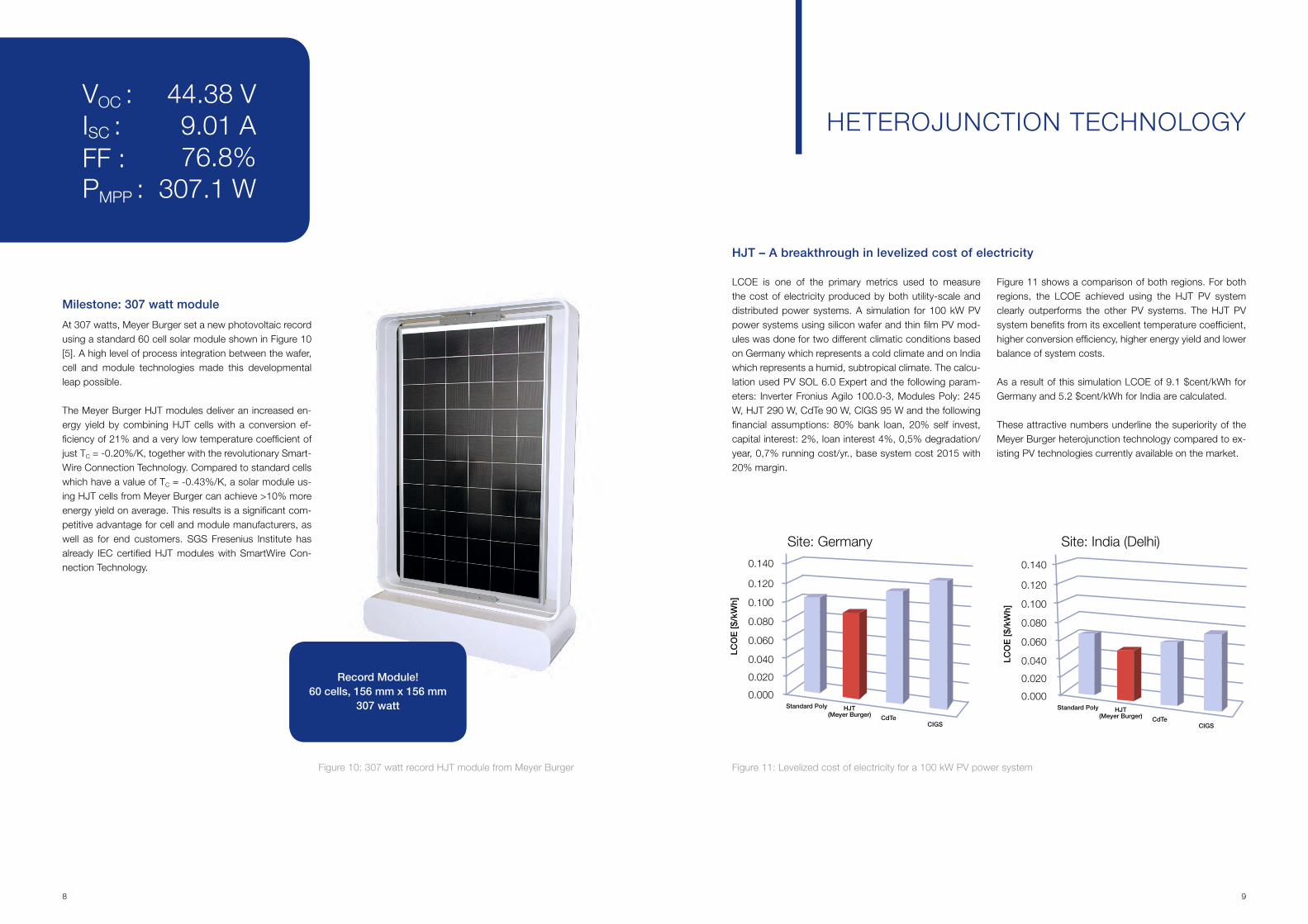
Milestone: 307 watt module
At 307 watts, Meyer Burger set a new photovoltaic record using a standard 60 cell solar module shown in Figure 10 [5]. A high level of process integration between the wafer, cell and module technologies made this developmental leap possible.
The Meyer Burger HJT modules deliver an increased en-ergy yield by combining HJT cells with a conversion ef-ficiency of 21% and a very low temperature coefficient of just TC = -0.20%/K, together with the revolutionary Smart-Wire Connection Technology. Compared to standard cells which have a value of TC = -0.43%/K, a solar module us-ing HJT cells from Meyer Burger can achieve >10% more energy yield on average. This results is a significant com-petitive advantage for cell and module manufacturers, as well as for end customers. SGS Fresenius Institute has already IEC certified HJT modules with SmartWire Con-nection Technology.
VOC : 44.38 VISC : 9.01 AFF : 76.8%PMPP : 307.1 W
Record Module!60 cells, 156 mm x 156 mm
307 watt
Figure 10: 307 watt record HJT module from Meyer Burger
HJT – A breakthrough in levelized cost of electricity
LCOE is one of the primary metrics used to measure the cost of electricity produced by both utility-scale and distributed power systems. A simulation for 100 kW PV power systems using silicon wafer and thin film PV mod-ules was done for two different climatic conditions based on Germany which represents a cold climate and on India which represents a humid, subtropical climate. The calcu-lation used PV SOL 6.0 Expert and the following param-eters: Inverter Fronius Agilo 100.0-3, Modules Poly: 245 W, HJT 290 W, CdTe 90 W, CIGS 95 W and the following financial assumptions: 80% bank loan, 20% self invest, capital interest: 2%, loan interest 4%, 0,5% degradation/year, 0,7% running cost/yr., base system cost 2015 with 20% margin.
LCO
E [$
/kW
h]
0.140
0.120
0.100
0.080
0.060
0.040
0.020
0.000Standard Poly
Site: Germany
HJT(Meyer Burger) CdTe
CIGS
LCO
E [$
/kW
h]
0.140
0.120
0.100
0.080
0.060
0.040
0.020
0.000Standard Poly HJT
(Meyer Burger) CdTeCIGS
Site: India (Delhi)
Figure 11: Levelized cost of electricity for a 100 kW PV power system
Figure 11 shows a comparison of both regions. For both regions, the LCOE achieved using the HJT PV system clearly outperforms the other PV systems. The HJT PV system benefits from its excellent temperature coefficient, higher conversion efficiency, higher energy yield and lower balance of system costs.
As a result of this simulation LCOE of 9.1 $cent/kWh for Germany and 5.2 $cent/kWh for India are calculated.
These attractive numbers underline the superiority of the Meyer Burger heterojunction technology compared to ex-isting PV technologies currently available on the market.
HETEROJUNCTION TECHNOLOGY
10 11
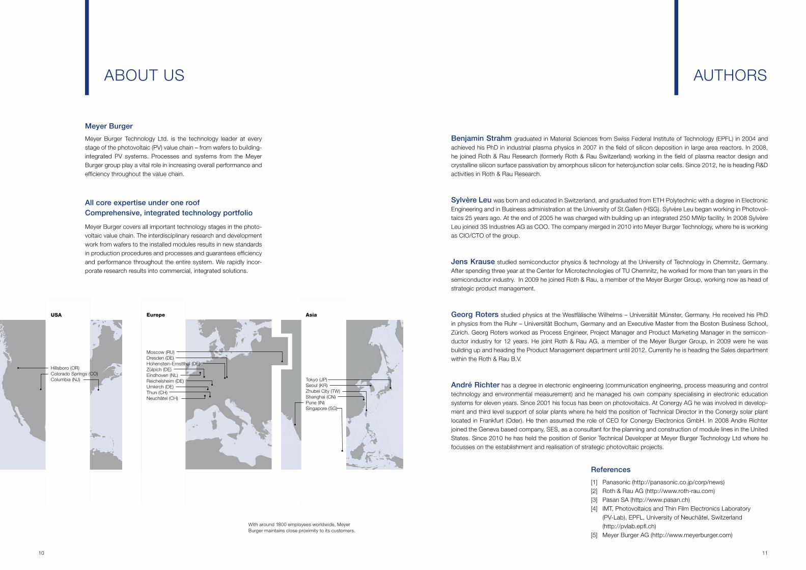
USA
Hillsboro (OR)Colorado Springs (CO)Columbia (NJ)
AUTHORS
With around 1800 employees worldwide, Meyer Burger maintains close proximity to its customers.
Asia
Tokyo (JP)Seoul (KR)Zhubei City (TW)Shanghai (CN)Pune (IN)Singapore (SG)
Europe
Moscow (RU)Dresden (DE)Hohenstein-Ernstthal (DE)Zülpich (DE)Eindhoven (NL)Reichelsheim (DE)Umkirch (DE)Thun (CH)Neuchâtel (CH)
ABOUT US
Meyer Burger
Meyer Burger Technology Ltd. is the technology leader at every stage of the photovoltaic (PV) value chain – from wafers to building-integrated PV systems. Processes and systems from the Meyer Burger group play a vital role in increasing overall performance and efficiency throughout the value chain.
All core expertise under one roof Comprehensive, integrated technology portfolio
Meyer Burger covers all important technology stages in the photo-voltaic value chain. The interdisciplinary research and development work from wafers to the installed modules results in new standards in production procedures and processes and guarantees efficiency and performance throughout the entire system. We rapidly incor-porate research results into commercial, integrated solutions.
Benjamin Strahm graduated in Material Sciences from Swiss Federal Institute of Technology (EPFL) in 2004 and achieved his PhD in industrial plasma physics in 2007 in the field of silicon deposition in large area reactors. In 2008, he joined Roth & Rau Research (formerly Roth & Rau Switzerland) working in the field of plasma reactor design and crystalline silicon surface passivation by amorphous silicon for heterojunction solar cells. Since 2012, he is heading R&D activities in Roth & Rau Research.
Sylvère Leu was born and educated in Switzerland, and graduated from ETH Polytechnic with a degree in Electronic Engineering and in Business administration at the University of St.Gallen (HSG). Sylvère Leu began working in Photovol-taics 25 years ago. At the end of 2005 he was charged with building up an integrated 250 MWp facility. In 2008 Sylvère Leu joined 3S Industries AG as COO. The company merged in 2010 into Meyer Burger Technology, where he is working as CIO/CTO of the group.
Jens Krause studied semiconductor physics & technology at the University of Technology in Chemnitz, Germany. After spending three year at the Center for Microtechnologies of TU Chemnitz, he worked for more than ten years in the semiconductor industry. In 2009 he joined Roth & Rau, a member of the Meyer Burger Group, working now as head of strategic product management.
Georg Roters studied physics at the Westfälische Wilhelms – Universität Münster, Germany. He received his PhD in physics from the Ruhr – Universität Bochum, Germany and an Executive Master from the Boston Business School, Zürich. Georg Roters worked as Process Engineer, Project Manager and Product Marketing Manager in the semicon-ductor industry for 12 years. He joint Roth & Rau AG, a member of the Meyer Burger Group, in 2009 were he was building up and heading the Product Management department until 2012. Currently he is heading the Sales department within the Roth & Rau B.V.
André Richter has a degree in electronic engineering (communication engineering, process measuring and control technology and environmental measurement) and he managed his own company specialising in electronic education systems for eleven years. Since 2001 his focus has been on photovoltaics. At Conergy AG he was involved in develop-ment and third level support of solar plants where he held the position of Technical Director in the Conergy solar plant located in Frankfurt (Oder). He then assumed the role of CEO for Conergy Electronics GmbH. In 2008 Andre Richter joined the Geneva based company, SES, as a consultant for the planning and construction of module lines in the United States. Since 2010 he has held the position of Senior Technical Developer at Meyer Burger Technology Ltd where he focusses on the establishment and realisation of strategic photovoltaic projects.
References
[1] Panasonic (http://panasonic.co.jp/corp/news)[2] Roth & Rau AG (http://www.roth-rau.com)[3] Pasan SA (http://www.pasan.ch)[4] IMT, Photovoltaics and Thin Film Electronics Laboratory (PV-Lab), EPFL, University of Neuchâtel, Switzerland (http://pvlab.epfl.ch)[5] Meyer Burger AG (http://www.meyerburger.com)

Meyer Burger Technology LtdSchorenstrasse 39 / 3645 Gwatt (Thun) / SwitzerlandPhone +41 33 221 28 00 / Fax +41 33 221 28 [email protected] / www.meyerburger.com H
JT-E
N-0
1
PASSIONATE ABOUT PV


