High performance CMOS based LC-VCO design using high Q-factor, field shield layered substrate inductor 1 Sarika M.R., 2 Karthigha Balamurugan Department of Electronics and Communication Engineering, Amrita School of Engineering, Coimbatore, Amrita Vishwa Vidyapeetham, India 1 [email protected], 2 [email protected]Abstract - This work reports a CMOS based current reuse voltage controlled oscillator (VCO) using the design of ferrite integrated inductor on a three layered substrate in order to obtain lower phase noise and to improve the FOM of the VCO. This work is focused on improving Q-factor and L-density of the inductor that is to be used in the VCO by the enhancement of the magnetic properties of the inductor core, optimizing geometry of the core as well as conductor and by isolation of the substrate. It is observed that the proposed ferrite integrated inductor with field shield substrate layer improves the Q-factor by 53.8% and L-density by 78.1% as compared to air core inductor. The 65 nm CMOS based current reuse LC-VCO designed using the proposed inductor operates in the (2.27-2.79) GHz range. The proposed VCO exhibits lower phase noise of -115.96 dBc/Hz and -135.01 dBc/Hz at an offset of 1 MHz and 5 MHz respectively. Measurements show that the proposed VCO consumes a power of 2.85 mW from a supply of 1.1 V. This demonstrates that the proposed inductor can be beneficial for high performance RF ICs. Index terms – Q-factor, ferrite-core inductor, field shield layer, substrate effects, phase noise, current reuse VCO I. INTRODUCTION With the advancements of CMOS technology in the recent years, there is an ever growing demand for high performance RF ICs in high speed, low power and high bandwidth communication systems. Technology scaling plays a pivotal role in advancement of ICs along with the use of circuit techniques. In particular, CMOS scaling has made RF CMOS IC design viable. VCO is identified as a challenging component in RF transceivers, and has been the driving force behind the endeavours to develop low power and compact RF ICs. VCOs are used for frequency conversion of the received signal to the intermediate frequency range with the help of a mixer in the front end of the receiver. On-chip spiral inductor is a key component of the VCO and is a deciding factor behind the performance parameters of the VCO namely phase noise, frequency tuning range and its figure-of-merit (FOM). Conventional on-chip inductors suffer from large size, low quality factor and low L-density, resulting from conductor losses and substrate losses, which are inevitable. Eddy current loss and resistive loss contribute to the conductor loss. The conductor loss in an on-chip spiral inductor is directly proportional to its series resistance which increases with frequency. This effect is given as , skin depth and related to frequency as in eq. (1). =√ (1) where in ‘ρ’ is the metal resistivity, ‘µ’ is the permeability and ‘f’ is the operating frequency. As a result of decrease in , series resistance increases. Eddy currents, contributes to both conductor and substrate losses, causing reduction in the spiral inductance and increases power losses in the substrate. In addition, the effect of parasitic capacitance due to oxide and other adjacent devices increases the complexity of inductor modeling. This motivates the inductor design to focus on reducing the conductor and substrate losses for improving the Q-factor and L-density. Non-availability of small size, high Q-factor and high L-density inductors pose a hindrance in the design of VCOs. Previous efforts have focused to develop various magnetic-core inductors for high Q-factor and high L- density, such as inductors with patterned magnetic dots. This design exhibits lower inductance value at high frequencies [1]. In other works, a grounded poly shield is used to reduce substrate loss and reported that they have not taken into account the process conditions [2,3]. In [4], solenoidal inductors with patterned permalloy magnetic cores were designed but suffered from eddy current losses at high frequencies. In [5], helical inductor with filtering method was designed but occupied large area. Moreover, the use of non- silicon substrates with high resistivity [6] to reduce substrate losses resulted in device failure due to non-uniform thermal expansion. In [7,8], the physical layout of the inductor was optimized but the relation between inductor performance and an individual variable was not known as it was based on multi- variable method. International Journal of Pure and Applied Mathematics Volume 119 No. 12 2018, 13759-13769 ISSN: 1314-3395 (on-line version) url: http://www.ijpam.eu Special Issue ijpam.eu 13759
Transcript
High performance CMOS based LC-VCO designusing high Q-factor, field shield
Abstract - This work reports a CMOS based current reusevoltage controlled oscillator (VCO) using the design of ferriteintegrated inductor on a three layered substrate in order toobtain lower phase noise and to improve the FOM of the VCO.This work is focused on improving Q-factor and L-density of theinductor that is to be used in the VCO by the enhancement of themagnetic properties of the inductor core, optimizing geometry ofthe core as well as conductor and by isolation of the substrate. Itis observed that the proposed ferrite integrated inductor withfield shield substrate layer improves the Q-factor by 53.8% andL-density by 78.1% as compared to air core inductor. The 65nm CMOS based current reuse LC-VCO designed using theproposed inductor operates in the (2.27-2.79) GHz range. Theproposed VCO exhibits lower phase noise of -115.96 dBc/Hz and-135.01 dBc/Hz at an offset of 1 MHz and 5 MHz respectively.Measurements show that the proposed VCO consumes a powerof 2.85 mW from a supply of 1.1 V. This demonstrates that theproposed inductor can be beneficial for high performance RFICs.
Index terms – Q-factor, ferrite-core inductor, field shield layer,substrate effects, phase noise, current reuse VCO
I. INTRODUCTION
With the advancements of CMOS technology in the recentyears, there is an ever growing demand for high performanceRF ICs in high speed, low power and high bandwidthcommunication systems. Technology scaling plays a pivotalrole in advancement of ICs along with the use of circuittechniques. In particular, CMOS scaling has made RF CMOSIC design viable. VCO is identified as a challengingcomponent in RF transceivers, and has been the driving forcebehind the endeavours to develop low power and compact RFICs. VCOs are used for frequency conversion of the receivedsignal to the intermediate frequency range with the help of amixer in the front end of the receiver. On-chip spiral inductoris a key component of the VCO and is a deciding factorbehind the performance parameters of the VCO namely phasenoise, frequency tuning range and its figure-of-merit (FOM).
Conventional on-chip inductors suffer from large size,low quality factor and low L-density, resulting fromconductor losses and substrate losses, which are inevitable.Eddy current loss and resistive loss contribute to the conductorloss. The conductor loss in an on-chip spiral inductor isdirectly proportional to its series resistance which increaseswith frequency. This effect is given as , skin depth andrelated to frequency as in eq. (1).= √ (1)
where in ‘ρ’ is the metal resistivity, ‘µ’ is the permeability and‘f’ is the operating frequency. As a result of decrease in ,series resistance increases. Eddy currents, contributes to bothconductor and substrate losses, causing reduction in the spiralinductance and increases power losses in the substrate. Inaddition, the effect of parasitic capacitance due to oxide andother adjacent devices increases the complexity of inductormodeling. This motivates the inductor design to focus onreducing the conductor and substrate losses for improving theQ-factor and L-density. Non-availability of small size, highQ-factor and high L-density inductors pose a hindrance in thedesign of VCOs. Previous efforts have focused to developvarious magnetic-core inductors for high Q-factor and high L-density, such as inductors with patterned magnetic dots. Thisdesign exhibits lower inductance value at high frequencies [1].In other works, a grounded poly shield is used to reducesubstrate loss and reported that they have not taken intoaccount the process conditions [2,3]. In [4], solenoidalinductors with patterned permalloy magnetic cores weredesigned but suffered from eddy current losses at highfrequencies. In [5], helical inductor with filtering method wasdesigned but occupied large area. Moreover, the use of non-silicon substrates with high resistivity [6] to reduce substratelosses resulted in device failure due to non-uniform thermalexpansion. In [7,8], the physical layout of the inductor wasoptimized but the relation between inductor performance andan individual variable was not known as it was based on multi-variable method.
International Journal of Pure and Applied MathematicsVolume 119 No. 12 2018, 13759-13769ISSN: 1314-3395 (on-line version)url: http://www.ijpam.euSpecial Issue ijpam.eu
13759
In a nutshell, the design of high Q-factor and high L-density inductor requires both geometrical considerations ofthe core and conductor as well as minimization of substratelosses which were not taken into account simultaneously in[1] - [8]. The proposed work focuses on improving Q-factorand L-density by enhancement of the magnetic properties ofthe core, by determination of optimal geometrical variables ofthe conductor and by isolation of the substrate. This isachieved by designing a ferrite integrated inductor whichhelps to increase the magnetic flux in the core. Next thegeometrical optimization of core and conductor is done withinthe area constraint .i.e the analysis of variation of Q and Lwith respect to geometrical parameters such as thickness of thecore, inner diameter and width of the spiral, helps inoptimization of the inductor design. This is followed byinserting the field shield layer to decouple the substrate frominductor. The substrate is designed as a three layered structurein which the field shield layer is placed in between the highresistivity substrate and low resistivity substrate so as to arrestthe carrier movement, thus reducing substrate losses and toavoid non-uniform thermal expansion problems.Thus the proposed work aims in developing a CMOS basedcurrent reuse LC-VCO in 65 nm to operate in the UWB bandusing the optimized ferrite integrated spiral inductor to cater tothe performance requirements of the VCO such as low powerconsumption, low phase noise, and a much improved FOM.The phase noise of VCO is decreased by enhancing the tankcircuit Q-factor. The tank Q-factor is improved by the properdesign of on-chip spiral inductor with reduced conductor andsubstrate losses. Based on these objectives, the paper isorganised as follows: section II analyses the factors that affectthe Q-factor and presents the circuit model of the optimizedferrite-core inductors, section III deals with the design of VCOincorporating the proposed inductors, section IV analyses theresults of the proposed inductor and VCO parameters andsection V is the conclusion.
II. DESIGN OF FERRITE INTEGRATED INDUCTOR
Integrated Passive Devices(IPD) technology uses threetypes of inductors, namely the planar spiral coil inductor, thesolenoidal inductor, and the multi-level spiral inductor. Planarspiral inductors are mostly preferred for RF ICs compared toothers due to their properties of high Q-factor, large value ofinductance and small size. The proposed design of spiralinductor consists of four types of inductor with respect tofilling of core, conductor geometry and substrate structureand are termed as L-1, L-2, L-3 and L-4.
A. Air-core inductorThe air-core inductor (L-1) is designed in HFSS with 2.5
turns, metal line width of 15 µm and spacing between turns as1.5 µm with an area of 450×450 µm. The structure of L-1, theair-core spiral inductor is shown in Fig. 1. It is made of a pairof spirals which are inter-wound and fabricated on differentmetal layers (M5 and M6) with an air-bridge, resulting inincreased current capacity and a decreased series resistance.
Due to the distance between the turns, capacitance presentbetween the adjacent turns is minimized. The spiral inductorcenter trap is connected to the remaining part of the circuit bythe air-bridge. Fig. 2 shows the equivalent model of L-1. The
Fig. 1 Layout of L-1.
Fig. 2 Equivalent model of air-core inductor
inductance of the spiral is represented by series inductance Ls
and its series resistance is given by Rs. The spiral andunderpass overlap capacitance is represented by the seriescapacitance Cs, Cbridge is the air-bridge capacitance and Cox isthe oxide capacitance. The capacitance of the substrate isrepresented by Csu and its resistance is represented by Rsu.
The electromagnetic coupling resulting from theseparasitic capacitances makes the inductor modeling difficult.Moreover, parasitic capacitance needs to be reduced so thatthe self-resonance frequency (SRF) of designed inductor doesnot fall inside the operating frequency range. Based on [9], theQ and L values for the L-1 is observed to be 6.85 and 2.11 nHrespectively from HFSS simulations.
.B. Ferrite core inductor
The structure of the proposed ferrite integratedinductor(L-2) is shown in Fig. 3. The addition of the ferritematerial in the core improves mobility and self resonantfrequency of the spiral on-chip inductor[10,11] as compared toair core inductor. The depth of the ferrite filling is designed tobe along the boundary of the spiral inductor in such a waythat a closed magnetic circuit is formed. The properties of thematerials used in the magnetic core mostly governs theperformance of an inductor. For minimising the magneticlosses, the ferrite material selected in this work has aresistivity and permeability of 10 kΩ-cm and 1000respectively.
International Journal of Pure and Applied Mathematics Special Issue
13760
Fig. 3 Ferrite integrated inductor.
The inductance value of L-2 in this design is related to theferrite permeability as follows:= + [ ( )] ∗ (2)
where is the inductance due to the air-core, and thesecond term is the increase in inductance due to addition offerrite which is dependent on the permeability of the ferrite.
is the permeability of air, w, l and t are the, width, lengthand ferrite film thickness respectively. is thedemagnetization factor which depends on the patterning offerrite film.
In a similar manner, the quality factor is improved by:
Q = ωL/ R = (3)
where results from the conductor loss. is resultingfrom the magnetic loss tangent (tan ) of the ferrite. For highresistivity ferrites, hysteresis and eddy current losses arenegligible [12]-[15]. This result in low loss tangent andlow as tan . This improves Q-factor of L-2compared to L-1. In the proposed work, L-2 has the samegeometry as that of L-1 except for the ferrite film and hasbetter Q and L value of 9.07 and 3.87 nH respectively.
The Q-factor and inductance of the spiral inductordepends on the geometrical aspects and frequency. It is knownthat geometrical aspects include the number of turns, ringshapes, the width of the spiral, the spacing between adjacentturns of the spiral, and its inner diameter. The pitfalls of theprevious optimizations [7,8] which aimed to improve Q-factorwas that variables were analysed simultaneously rather than asingle variable at a time. In the proposed work, effect on Q-factor and L-density of L-2 for varying inner diameters, linewidths, ferrite permeability and substrate conductivity wereanalysed, considering one variable at a time. In addition,thickness of the ferrite material was varied to study its effecton Q-factor.
C. Ferrite core inductor with field shield substrate layerIn this work, the inductor L-3 is designed with a ferrite
core on a three layered substrate. The free background carrierconcentration is low in high resistivity Si substrates[16] –[18]. In [19], a physical model for inductor was developedincorporating substrate losses. Related work [20] involvedvertical self-assembly of spiral inductors to reduce substratelosses but integration became all the more complicated.
Moreover, the use of high resistivity non-Si substratesresults in non-uniform thermal expansion and led to devicefailure. Hence in the proposed L-3, the top layer substrate haslow conductivity of 1 S/m (highest resistivity), followed bythe field shield layer with conductivity of 2.5 S/m(moderateresistivity) and bottom layer with a higher conductivity of 5S/m(lowest resistivity). The increase in conductivity from topto bottom minimizes the substrate losses as the field shieldlayer isolates the lower layer substrate from the inductor.Thus, the proposed L-3 intend to possess lower conductor andsubstrate losses.
Fig. 4(a) shows the circuit model of the inductor L-3. The parameters introduced by the addition of ferritematerial and the field shield layer are the following: the realpart of permeability introduces Lf to Ls, the imaginary part ofpermeability introduces Rf to Rs, due to the addition of ferrite.Cf-lap is the series capacitance added to Cs, Cf-1 is thecapacitance added between inductor coils, Cf -2 and Cf -3 are theseries and shunt capacitances respectively to Cox. Thesubstrate resistance of the three layered structure isrepresented by Rt, Rfs and Rb for top, field shield and bottomlayer respectively. The substrate capacitance for top, fieldshield and bottom layer Csub-1, Csub-2 and Csub-3 respectively.The substrate resistance and capacitance of each layer areconnected in parallel. The layout of the proposed inductor isdesigned and shown in Fig. 4(b). The Q and L values of L-3 isobserved to be 10.54 and 3.76 nH and 10.54 respectively andfound to be better than L-2.
Fig. 4(a): Equivalent circuit model for the inductor L-3
Fig. 4(b).Layout of the inductor
International Journal of Pure and Applied Mathematics Special Issue
13761
Considering the effect of substrate losses, the Q-factor for L-3can be expressed as:
Q = ∗ SRF * SLF (4)
where the self resonance factor (SRF) of L-3 is given by:= 1 − + + − ++ ) (5)The substrate loss factor (SLF) of L-3 is expressed as:= ( ) (6)
where = /( + + )As the decay of electric field in the substrate is
exponential, the contribution of each layer [21] is given by:
= (7)
= (8)
=( )
(9)where Rct, Rct, Rct are the contributions of resistances in top,field shied and bottom layers respectively. As seen from theeqn.(7-9), the top layer with thickness and field shield layerwith thickness reduces the electric field penetration intothe lower layer substrate, and thus increases. Then fromeqn. (6) SLF tends to unity which results in increase in Q-factor.
In order to study and compare the effect of substratelosses in the absence of field shield layer, another ferrite-coreinductor L-4 is designed on a two layered substrate i.e with nofield shield layer. For L-4, there is an abrupt change inconductivity from top to bottom layer as it has a two layeredsubstrate. Both L-3 and L-4 has same area as L-1 and L-2.The Q and L values of L-4 are found to be 12.39 and 3.74 nHrespectively. In simulation environment, high resistivitysubstrate occupying larger volume is considered as primaryadvantage without considering the electric field strength.Hence the Q-factor of L-4 is higher than L-3. The electric field
Fig. 5 (a) Electric field strength in substrate of L-3.
Fig. 5 (b) Electric field strength in substrate of L-4.
strength in the substrate of L-3 and L-4 is shown in Fig. 5(a)and Fig. 5(b).The Q and L values and the average value ofelectric field strength in the substrate layers of L-3 and L-4 areshown in Table I.
As seen from the Table I, the average electric fieldpenetration in substrate of L-3 is 3.76× 10³ V/m as comparedto 5.79× 10³ V/m in L-4 and this is due to the presence of fieldshield layer in L-3.This implies that the substrate losses in L-3is lesser than that of L-4 due to the presence of field shieldlayer. Section III deals with the integration of the proposedinductors L-1, L-2,L-3 and L-4 in the design of VCO.
III. VCO DESIGN USING INDUCTOR DESIGN
The inductor design and its optimization are followed bythe design of 65 nm CMOS based current reuse LC-VCOoperating in the UWB band. The main VCO parameters arephase noise, power and frequency tuning range and theseaffect the FOM. In this work, four VCO circuits (VCO-1,VCO-2, VCO-3 and VCO-4) are designed, with sameschematic, but utilising the four proposed inductors (i.e.,L-1,L-2, L-3 and L-4). For accurate evaluation of effect ofmagnetic enhancement in inductors, they have the same spiral
TABLE 1.COMPARISON OF L-3 AND L-4
Inductor
L(nH)Q Electric field strength(V/m)
Averageelectric field
strength(V/m)
3.76
(L-3)10.54
Top layer Middle layerBottom
layer3.76× 103
9.95 × 10³ 1.215 × 10³ 0.1255× 10³
3.74
(L-4)12.39
Top layerBottom
layer5.79× 103
11.44× 1030.14325×
103
International Journal of Pure and Applied Mathematics Special Issue
13762
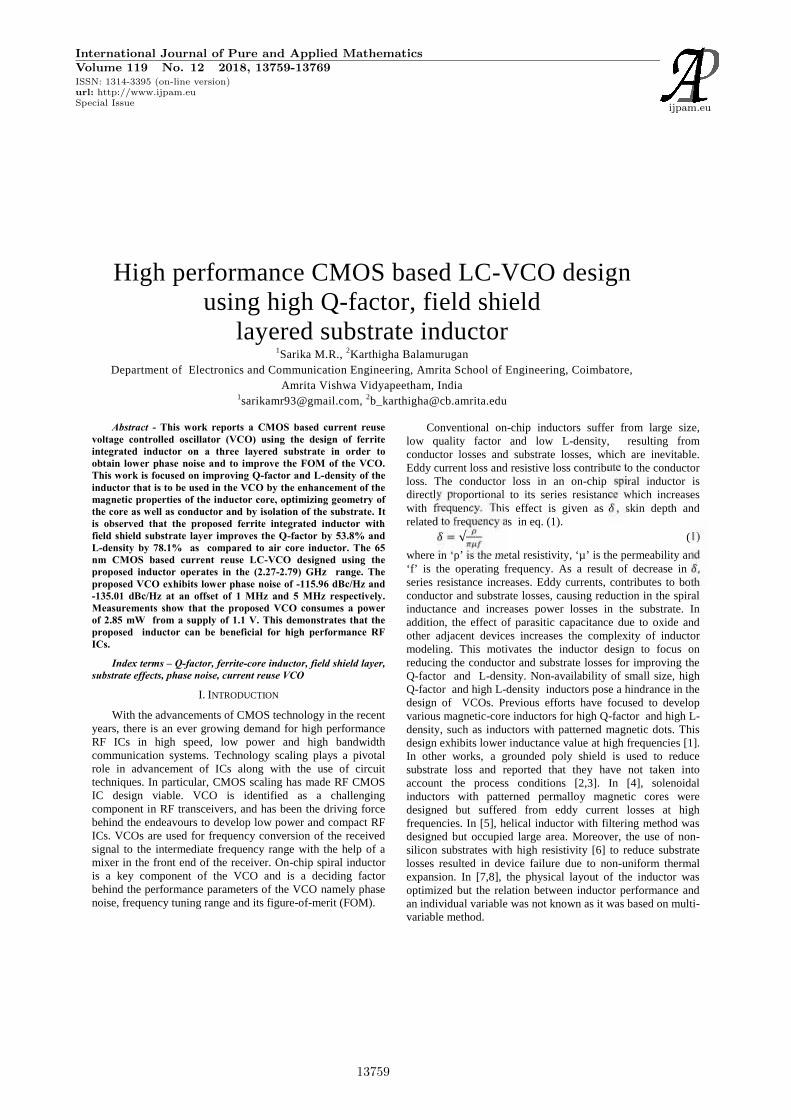
width, spacing between turns, and metal stack. The air-coreinductor (L-1) is used in VCO-1, VCO-2 utilizes the ferrite-core inductor (L-2), VCO-3 utilises the magnetic coredinductor, L-3 designed on a three layered substrate using fieldshield layer as intermediate layer and VCO-4 utilises L-4. Anegative-resistance LC-VCO topology is shown in the Fig. 6with an LC tank (L,M5 and M6) where the proposed inductordesigns forms L and cross coupled NMOS transistor pairs asdriver(M3 and M4) and PMOS as load (M1 and M2).
In the tank circuit, varactor (M5 and M6) forms C, whichare used for frequency tuning. The varactors M5 and M6 aremodeled by connecting the drain and source of the NMOStransistor together to act as one terminal and the other terminalis the gate. PMOS is used due to its low flicker noise. Both theload and driver have the same current flowing through themand offers the negative resistance necessary to compensate forthe losses in the tank. For the purpose of reducing power,current reuse topology is widely used in RF circuits [22-23].The switching transistors are cross connected thus resulting inthe reuse of dc bias current as during the first half cycle of theoutput, the combination of PMOS (M2) and NMOS (M3) are intriode region and acts like a closed switch thus charging up thevaractor in the tank.During the next half cycle, M2 and M3 are open and the tankdischarges through M1 and M4. Thus, the current is drawnfrom the supply only for one half cycle, and in the next halfcycle output signal is continued by the discharge current fromthe tank. Hence, the power dissipation of the circuit is reducedby current reuse. The frequency tuning of VCO is achievedwith the help of varactor in the tank as it offers variablecapacitance when the control voltage (Vctrl) applied to the gateof the varactor is varied. The frequency tuning range is furtherimproved by using a switched capacitor array as shown by C1
and C2. Due to limited tuning capacity of NMOS varactors, in-built varactors are preferred. This VCO topology is integratedwith the proposed spiral inductor structure (L) andperformance parameters of VCO such as phase noise, powerconsumption, frequency tuning range and FOM are analysed.The loss resistance of the LC tank circuit shown in Fig.7is given by the equation= √( ) (10)
where is the quality factor of the tank. will be highwhen is maximum.Rn is the negative resistance offered by the MOS transistorpairs and should balance the losses in the tank to sustainoscillations(Rn= Rp). is given by:= + (11)
where = / and = 1/CRof varactors is generally high and can be neglected which
means = . The Q-factor of a conventional spiral inductoris usually limited by its conductor and substrate losses. Henceit is inherent that designing an inductor with high L-densityand Q-factor is crucial to maximize . Thus, the design ofhigh Q-factor inductor is important in the design of VCO.Moreover, the startup condition for oscillation in a negative-resistance VCO is given by
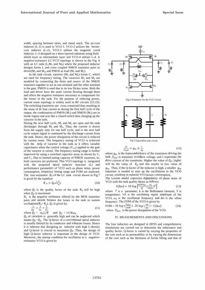
Fig.6 Schematic for the VCO circuit
F
Fig.7.Equivalent tank circuit= ≥ (12)
where is the transconductance of the transistors driving thetank , is transistor overdrive voltage, and I represents thedrive current of the transistors. Higher the value of , higherwill be the value of and this results in low value of. Thus, if the Q-factor of the inductor is high, a smallertransistor is needed to start up the oscillations in the VCOcircuit, resulting in reduced VCO power consumption.The Leeson model expresses dependency of phase noise ofVCO with the tank quality factor as follows:∆ = 10 ( ∆ ) (13)
where F is a parameter, k is the Boltzmann constant, T istemperature, V0 is the oscillating signal amplitude of theVCO, is the oscillation frequency and ∆ is the offsetfrequency. The FOM of the VCO is given by
FOM = 10 ( )– 20 ( ∆ ) + ∆ (14)
where is the power dissipation of the VCO.
IV. MEASUREMENTS AND DISCUSSIONS
The four inductors are designed in HFSS and comprehensivesimulations are carried out to determine the inductance andquality factor. Q-factor is varied by varying the properties ofthe core such as its permeability or by varying the dimensionsof the core such as the thickness of ferrite filling and that of
width, spacing between turns, and metal stack. The air-coreinductor (L-1) is used in VCO-1, VCO-2 utilizes the ferrite-core inductor (L-2), VCO-3 utilises the magnetic coredinductor, L-3 designed on a three layered substrate using fieldshield layer as intermediate layer and VCO-4 utilises L-4. Anegative-resistance LC-VCO topology is shown in the Fig. 6with an LC tank (L,M5 and M6) where the proposed inductordesigns forms L and cross coupled NMOS transistor pairs asdriver(M3 and M4) and PMOS as load (M1 and M2).
In the tank circuit, varactor (M5 and M6) forms C, whichare used for frequency tuning. The varactors M5 and M6 aremodeled by connecting the drain and source of the NMOStransistor together to act as one terminal and the other terminalis the gate. PMOS is used due to its low flicker noise. Both theload and driver have the same current flowing through themand offers the negative resistance necessary to compensate forthe losses in the tank. For the purpose of reducing power,current reuse topology is widely used in RF circuits [22-23].The switching transistors are cross connected thus resulting inthe reuse of dc bias current as during the first half cycle of theoutput, the combination of PMOS (M2) and NMOS (M3) are intriode region and acts like a closed switch thus charging up thevaractor in the tank.During the next half cycle, M2 and M3 are open and the tankdischarges through M1 and M4. Thus, the current is drawnfrom the supply only for one half cycle, and in the next halfcycle output signal is continued by the discharge current fromthe tank. Hence, the power dissipation of the circuit is reducedby current reuse. The frequency tuning of VCO is achievedwith the help of varactor in the tank as it offers variablecapacitance when the control voltage (Vctrl) applied to the gateof the varactor is varied. The frequency tuning range is furtherimproved by using a switched capacitor array as shown by C1
and C2. Due to limited tuning capacity of NMOS varactors, in-built varactors are preferred. This VCO topology is integratedwith the proposed spiral inductor structure (L) andperformance parameters of VCO such as phase noise, powerconsumption, frequency tuning range and FOM are analysed.The loss resistance of the LC tank circuit shown in Fig.7is given by the equation= √( ) (10)
where is the quality factor of the tank. will be highwhen is maximum.Rn is the negative resistance offered by the MOS transistorpairs and should balance the losses in the tank to sustainoscillations(Rn= Rp). is given by:= + (11)
where = / and = 1/CRof varactors is generally high and can be neglected which
means = . The Q-factor of a conventional spiral inductoris usually limited by its conductor and substrate losses. Henceit is inherent that designing an inductor with high L-densityand Q-factor is crucial to maximize . Thus, the design ofhigh Q-factor inductor is important in the design of VCO.Moreover, the startup condition for oscillation in a negative-resistance VCO is given by
Fig.6 Schematic for the VCO circuit
F
Fig.7.Equivalent tank circuit= ≥ (12)
where is the transconductance of the transistors driving thetank , is transistor overdrive voltage, and I represents thedrive current of the transistors. Higher the value of , higherwill be the value of and this results in low value of. Thus, if the Q-factor of the inductor is high, a smallertransistor is needed to start up the oscillations in the VCOcircuit, resulting in reduced VCO power consumption.The Leeson model expresses dependency of phase noise ofVCO with the tank quality factor as follows:∆ = 10 ( ∆ ) (13)
where F is a parameter, k is the Boltzmann constant, T istemperature, V0 is the oscillating signal amplitude of theVCO, is the oscillation frequency and ∆ is the offsetfrequency. The FOM of the VCO is given by
FOM = 10 ( )– 20 ( ∆ ) + ∆ (14)
where is the power dissipation of the VCO.
IV. MEASUREMENTS AND DISCUSSIONS
The four inductors are designed in HFSS and comprehensivesimulations are carried out to determine the inductance andquality factor. Q-factor is varied by varying the properties ofthe core such as its permeability or by varying the dimensionsof the core such as the thickness of ferrite filling and that of
International Journal of Pure and Applied Mathematics Special Issue
13763
the conductor like its inner diameter, width or by varying theproperties of the substrate such as its conductivity.
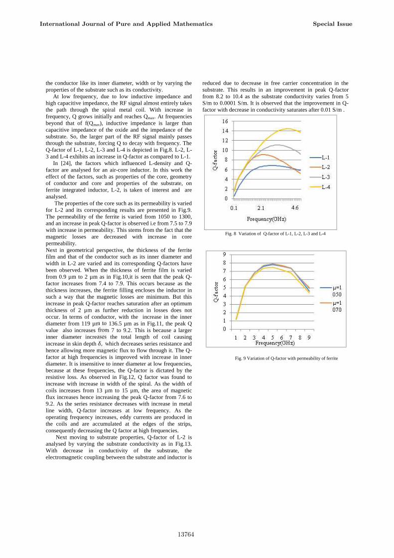
At low frequency, due to low inductive impedance andhigh capacitive impedance, the RF signal almost entirely takesthe path through the spiral metal coil. With increase infrequency, Q grows initially and reaches Qmax. At frequenciesbeyond that of f(Qmax), inductive impedance is larger thancapacitive impedance of the oxide and the impedance of thesubstrate. So, the larger part of the RF signal mainly passesthrough the substrate, forcing Q to decay with frequency. TheQ-factor of L-1, L-2, L-3 and L-4 is depicted in Fig.8. L-2, L-3 and L-4 exhibits an increase in Q-factor as compared to L-1.
In [24], the factors which influenced L-density and Q-factor are analysed for an air-core inductor. In this work theeffect of the factors, such as properties of the core, geometryof conductor and core and properties of the substrate, onferrite integrated inductor, L-2, is taken of interest and areanalysed.
The properties of the core such as its permeability is variedfor L-2 and its corresponding results are presented in Fig.9.The permeability of the ferrite is varied from 1050 to 1300,and an increase in peak Q-factor is observed i.e from 7.5 to 7.9with increase in permeability. This stems from the fact that themagnetic losses are decreased with increase in corepermeability.Next in geometrical perspective, the thickness of the ferritefilm and that of the conductor such as its inner diameter andwidth in L-2 are varied and its corresponding Q-factors havebeen observed. When the thickness of ferrite film is variedfrom 0.9 µm to 2 µm as in Fig.10,it is seen that the peak Q-factor increases from 7.4 to 7.9. This occurs because as thethickness increases, the ferrite filling encloses the inductor insuch a way that the magnetic losses are minimum. But thisincrease in peak Q-factor reaches saturation after an optimumthickness of 2 µm as further reduction in losses does notoccur. In terms of conductor, with the increase in the innerdiameter from 119 µm to 136.5 µm as in Fig.11, the peak Qvalue also increases from 7 to 9.2. This is because a largerinner diameter increases the total length of coil causingincrease in skin depth , which decreases series resistance andhence allowing more magnetic flux to flow through it. The Q-factor at high frequencies is improved with increase in innerdiameter. It is insensitive to inner diameter at low frequencies,because at these frequencies, the Q-factor is dictated by theresistive loss. As observed in Fig.12, Q factor was found toincrease with increase in width of the spiral. As the width ofcoils increases from 13 µm to 15 µm, the area of magneticflux increases hence increasing the peak Q-factor from 7.6 to9.2. As the series resistance decreases with increase in metalline width, Q-factor increases at low frequency. As theoperating frequency increases, eddy currents are produced inthe coils and are accumulated at the edges of the strips,consequently decreasing the Q factor at high frequencies.
Next moving to substrate properties, Q-factor of L-2 isanalysed by varying the substrate conductivity as in Fig.13.With decrease in conductivity of the substrate, theelectromagnetic coupling between the substrate and inductor is
reduced due to decrease in free carrier concentration in thesubstrate. This results in an improvement in peak Q-factorfrom 8.2 to 10.4 as the substrate conductivity varies from 5S/m to 0.0001 S/m. It is observed that the improvement in Q-factor with decrease in conductivity saturates after 0.01 S/m .
Fig. 8 Variation of Q-factor of L-1, L-2, L-3 and L-4
Fig. 9 Variation of Q-factor with permeability of ferrite
International Journal of Pure and Applied Mathematics Special Issue
13764
Fig. 10. Variation of Q-factor with ferrite thickness
Fig. 11. Variation of Q-factor with inner diameter
Fig. 12. Variation of Q-factor with width
Fig. 13.Variation of Q-factor with substrate conductivity
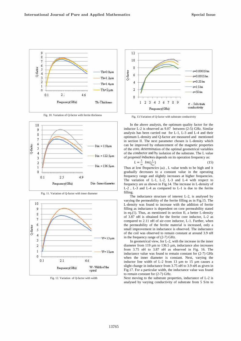
In the above analysis, the optimum quality factor for theinductor L-2 is observed as 9.07 between (2-5) GHz. Similaranalysis has been carried out for L-1, L-3 and L-4 and theiroptimum L-density and Q-factor are measured and mentionedin section II. The next parameter chosen is L-density whichcan be improved by enhancement of the magnetic propertiesof the core, determination of the optimal geometrical variablesof the conductor and by isolation of the substrate. The L valueof proposed inductors depends on its operation frequency as:= ( ) (15)
Thus at low frequencies (ω) , L value tends to be high and itgradually decreases to a constant value in the operatingfrequency range and slightly increases at higher frequencies.The variation of L-1, L-2, L-3 and L-4 with respect tofrequency are as shown in Fig.14. The increase in L-density ofL-2 , L-3 and L-4 as compared to L-1 is due to the ferritefilling.
The inductance structure of interest L-2, is analysed byvarying the permeability of the ferrite filling as in Fig.15. TheL-density was found to increase with the addition of ferritefilling as inductance is dependent on core permeability statedin eq.(1). Thus, as mentioned in section II, a better L-densityof 3.87 nH is obtained for the ferrite core inductor, L-2 ascompared to 2.11 nH of air-core inductor, L-1. Further, whenthe permeability of the ferrite material is increased, only asmall improvement in inductance is observed. The inductanceof the coil was observed to remain constant at around 3.9 nHin the frequency range of (2-7) GHz.
In geometrical view, for L-2, with the increase in the innerdiameter from 119 µm to 136.5 µm, inductance also increasesfrom 3.75 nH to 3.87 nH as observed in Fig. 16. Theinductance value was found to remain constant for (2-7) GHzwhen the inner diameter is constant. Next, varying theinductor line width of L-2 from 13 µm to 15 µm causes aslight change in inductance from 3.75 nH to 3.9 nH as given inFig.17. For a particular width, the inductance value was foundto remain constant for (2-7) GHz.Next moving to the substrate properties, inductance of L-2 isanalysed by varying conductivity of substrate from 5 S/m to
International Journal of Pure and Applied Mathematics Special Issue
13765
0.0001 S/m as in Fig. 18, the L value increased from 3.7 nH to3.9 nH. The L value continued to remain constant in the (2-5)GHz range at around 3.8 nH when the conductivity isconstant.
Based on the analysis, the optimum value of L-density ofL-2 is found to be 3.87 nH. Based on similar analysis,optimum values of L-density for L-1, L-3 and L-4 are obtainedand have been mentioned in section II.
Fig. 14. Variation of L-density of L-1, L-2, L-3 and L-4
Fig. 15. Variation of L with permeability of the ferrite
Fig. 16. Variation of L with inner diameter
Fig. 17. Variation of L with conductivity of the substrate
Fig. 18. Variation of L with width
International Journal of Pure and Applied Mathematics Special Issue
13766
Fig. 19. Phase noise of VCO
The inductor optimization and analysis are followed bythe simulation of VCOs designed in 65 nm CMOS usingcurrent reuse LC structure incorporating the proposedinductors [L-1, L-2, L-3 and L-4]. The corresponding VCOsare termed as VCO-1, VCO-2, VCO-3 and VCO-4respectively. PSS and PNOISE analysis available in ADE-Lwindow of Cadence Virtuoso are used to measure the phasenoise of VCO.
Fig. 19 shows the measured phase noise for the fourVCOs when the tuning voltage is varied from 0.1 to 1 V(Vctrl). The purpose of this work is to focus on the merits andfeasibility of utilizing the ferrite-cored inductor in the designof VCO. Hence, the frequency tuning overlap, which exists inthe conventional VCO designs, is not taken into account. Thecomparison of performance of the VCOs is given in Table II.The phase noise for VCO-1 are observed to be -114.6 dBc/Hz,-134.2 dBc/Hz and -142.22 dBc/Hz at 1 MHz, 5 MHz and 10MHz offset respectively. Similarly the phase noise for VCO-2, VCO-3 and VCO-4 are found to be -113.054 dBc/Hz, -132.37 dBc/Hz and -140.13 dBc/Hz, -115.96 dBc/Hz, -135.01 dBc/Hz and -142.66 dBc/Hz, and -101.83 dBc/Hz, -121.27 dBc/Hz and -129.14 dBc/Hz at 1MHz, 5MHz and 10MHz offset respectively.
Comparing the phase noise among the designed VCOs, at1 MHz, VCO-3 shows better result, that is, -115.96 dBc/Hzand similarly it gives the best performance at 5 MHz and at 10MHz, as -135.01 and -142.66 dBc/Hz. So the ferrite coreinductor using field shield layered inductor design (L-3) ismore suitable for VCO design.
From Table II, it is observed that VCO-1 using air-coreinductor L-1 shows better phase noise reduction than ferritecore inductor L-2 but at an expense of power. In case of thenegative-resistance driver pairs (M3, M4 and M1, M2), gm
required to start up the oscillation in the VCO is low whileusing ferrite integrated inductor because the Q-factor of L-2and L-3 is greater than that of L-1. This reduction in gm
lowers the power consumption of VCO, as validated inmeasurement, i.e. 3.3 mW for VCO-1, 2.64 mW for VCO-2and 2.85 mW for VCO-3 at a 1.1 V supply. Also, the phasenoise variation over the frequency range (1-10MHz) is lesserfor VCO-2 (27.08 dB), VCO-3 (26.7 dB) and VCO-4 (27.01dB) as compared to VCO-1(27.62 dB). Overall, VCO-3 withL-3 shows better phase noise reduction and lesser phase noisevariation than others due to improvement in Q-factor via
magnetic enhancement and field shield layer. Powerconsumption of VCO-3 is slightly greater than VCO-2 andVCO-4 but lesser than that of VCO-1. The FOM for VCO-1 ismeasured to be 177.7 dBc/Hz and VCO-2 is 177.1 dBc/Hz.VCO-3 has an FOM of 179.1 dBc/Hz and FOM of VCO-4 is170.2 dBc/Hz.
V. CONCLUSION
In order to cater to the necessary requirements of highperformance VCOs in RF-ICs, we have proposed an optimizedthe on-chip spiral inductor that gives better Q-factor by theintroduction of field shield layer in between a high resistivityand low resistivity substrate. The study focuses on variousfactors affecting the Q-factor - magnetic properties of the core,dimensions of the spiral, and properties of the substrate. Withthe magnetic enhancement of the core and field shield substratelayer, Q-factor is improved by 53.8% and L-density of theproposed inductor is improved by 78.1% when compared toair-core inductor. The power consumption of the VCO-3 withproposed inductor (L-3) is observed to be 2.85 mW at a 1.1 Vsupply and it exhibits a noticeable better phase noise of -142.66dBc/Hz at 10 MHz offset.
REFERENCES
[1]W. Xu, S. Sinha, F. Pan, T. Dastagir, Y. Cao, and H. Yu, “Improvedfrequency response of on-chip inductors with patterned magnetic dots,” IEEEElectron Device Letters (2010), vol. 31, no. 3, pp. 207–209.[2] T. Yoshitomi, Y. Sugawara, E. Morifuji, T. Ohguro, H. Kimijima, T.Morimoto, H. S. Momose, Y. Katsumata, H. Iwai, “On-chip spiral inductorswith diffused shields using channel-stop implant,” Int. Electron DevicesMeeting Tech. Dig.(1998), pp. 540-543.[3]C. P. Yue, S. S. Wong, “On-chip spiral inductors with patterned groundshields for Si-based RF ICs,” IEEE J. Solid-State Circuits(1998), vol. 33, no.5, pp. 743-752.[4]W. Xu, S. Sinha, T. Dastagir, H.Wu, B. Bakkaloglu, D. S. Gardner, andH.Yu, “Performance enhancement of on-chip inductors with Permalloymagnetic rings,” IEEE Electron Device Leters.(2011), vol. 32, no. 1, pp. 69–71.
TABLE.IICOMPARISON OF VCOs
VCOFrequency
(GHz)PN @1MHz,
@5MHz, @10MHz(dBc/Hz)
Power(mW)
Q L(nH)
VCO-1
2.25-2.82 -114.6, -134.2, -142.22
3.30 6.85 2.11
VCO-2
2.04-2.88 -113.05, -132.37, -140.13
2.64 9.07 3.87
VCO-3
2.27-2.79 -115.96, -135.01, -142.66
2.85 10.54 3.76
VCO-4
2.34-2.76 -101.83, -121.27, -129.14
2.65 12.39 3.74
International Journal of Pure and Applied Mathematics Special Issue
13767
[5]J. Gil, S. S. Song,H. Lee, and H. Shin, “A-119.2 dBc/Hz at1MHz, 1.5mW,fully integrated, 2.5-GHz, CMOS VCO using helical inductors,” IEEEMicrow. Wireless Compon. Letters (2003), vol. 13, no. 11, pp. 457–459.[6] Nenadovic N, D’Alessandro V, Nanver L, Tamigi F, Rinaldi N, Slotboom
J., “ A back wafer contacted silicon-on-glass integrated bipolar process. Part II:A novel analysis of thermal breakdown,” IEEE Trans Electron Dev. (2004),51(1):51–62.[7]C.J. Chao, S.C. Wong, C.H. Kao, M.J. Chen, L.Y. Leu, K.Y. Chiu,
“Characterization and modeling of on-chip spiral inductors for Si RFICs,”IEEE Trans. Semicond. Manuf. 15 (1) (2002), 19–29.[8] A. Nieuwoudt, Y. Massoud, “Optimizing the design of tunable spiralinductors for on-chip wireless applications,” IEEE Wireless and MicrowaveTechnology Conference, 2006.[9]Mohan SS, Hershenson MD, Boyd SP, Lee TH, “Simple accurateexpressions for planar spiral inductances,” IEEE J Solid-State Cir.(1999),34(10):1419–24.[10]C. Yang, F. Liu, A. Wang, J. Zhan, A. Wang, T. L. Ren, and X.Li,“Investigation of on-chip soft-ferrite-integrated inductors for RF ICs—Part I:Design and simulation,” IEEE Trans. Electron Devices (2009),vol. 56, no. 12,pp. 3133–3140.[11] Hua-Lin Cai, Yi Yang, Nan Qi, Xiao Chen, He Tian, Zheng Song, YangXu, Chang-Jian Zhou, , Jing Zhan, Albert Wang, Baoyong Chi, and Tian-LingRen, “A 2.7-mW 1.36–1.86-GHz LC-VCO With a FOM of 202 dBc/HzEnabled by a 26%-Size-Reduced Nano-Particle-Magnetic-EnhancedInductor,” IEEE transactions on microwave theory and techniques (2014),vol. 62, no. 5.[12]Kaneko, K., N. Inoue, N. Furutake, and Y. Hayashi, “A novelmultilayered Ni-Zn-ferrite/TaN film for RF/mobile applications,” Jpn. J. Appl.Phys. (2010), Vol. 49, No. 4, 04DB15-1–04DB15-5.[13]Qu, W., X. H. Wang, and L. Li, “Preparation and performance ofNiCuZn-Co2Z composite ferrite material,” J. of Magnetism and Maneticmaterias.(2003), Vol. 257, No. 2–3, 284–289.[14]Cai, H. L., J. Zhan, C. Yang, X. Chen, Y. Yang, B. Y. Chi, A. Wang, andT. L. Ren, “Application of ferrite nanomaterial in RF on-chip inductors,” J.Nanomateials (2013), Vol. 2013, 1–12.[15] Yang, C., F. Liu, X. Wang, J. Zhan, A. Wang, T. L. Ren, L. T. Liu, H.Long, Z. Wu, and X. Li, “Investigation of on-chip soft-ferrite-integratedinductors for RFICs — Part II: Experiments,” IEEE Trans. Electron Devices(2009), Vol. 56, No. 12, 3141–3148.[16]Fuchs C, Cadix L, Cheramy S, Charbonnier J, Farcy A., “ Simulation andcharacterization of silicon conductivity influence on HF behaviour of TSV,”In:12th Electronics packaging technology conference.[17]Barakat MH, Delaveaud C, Ndagijimana F.,”60 GHz high resistivitysilicon on insulator interdigitated dipole antenna,” Microw Opt Technol Lett(2010),52:1197.[18]Titz D, Pilard R, Ferrero F, Gianesello F, Gloria D, Luxey C, et al.,”60GHz antenna integrated on high resistivity silicon technologies targetingWHDMI applications,” In: IEEE radio frequency integrated circuitssymposium (RFIC).[19]Huo X, Chan PCH, Chen KJ, Luong HC.,”A physical model for on-chipspiral inductors with accurate substrate modelling,” IEEE Trans Electron Dev(2006),53:2942.[20]Kiziroglou M, Mukherjee A, Vatti S, Holmes A, Papavassiliou C,Yeatman E., “Self assembly of three-dimensional Au inductors on silicon,”IET Microw. Anten Propag (2009),4:1698–703.[21] Kanad Mallik, A. Abuelgasim, N. Hashim, P. Ashburn, C.H. de Groot.,,“Analytical and numerical model of spiral inductors on high resistivity siliconsubstrates ,” ELSEVIER, Solid-State Electronics 93 (2014) 43–48[22] Meng-Ting Hsu , Tsung-Han Han, Yao-Yen Lee., “ Design of Sub-1 mWCMOS LC VCO based on current reused topology with Q-enhancement andbody-biased technique,” Microelectronics Journal 45 (2014) 627–633[23] Sriharsha Ankathi, Sriramula Vignan, Srikanth Athukuri, Smrithi Mohan,Karthigha Balamurugan, M. Nirmala Devi., “ A 5–7 GHz current reuse and
gm-boosted common gate low noise amplifier with LC based ESD protectionin 32 nm CMOS,” Analog Integr Circ Sig Process (2017), 90:573–589[24]Cong Wang, Nam-Young Kim., “Analytical optimization of high-performance and high-yield spiral inductor in integrated passive devicetechnology,” Microelectronics Journal 43 (2012) 176–181.
International Journal of Pure and Applied Mathematics Special Issue