ACTA UNIVERSITATIS UPSALIENSIS UPPSALA 2008 Digital Comprehensive Summaries of Uppsala Dissertations from the Faculty of Science and Technology 407 High Aspect Ratio Microstructures in Flexible Printed Circuit Boards Process and Applications HANNA YOUSEF ISSN 1651-6214 ISBN 978-91-554-7127-9 urn:nbn:se:uu:diva-8565
Transcript
ACTA
UNIVERSITATIS
UPSALIENSIS
UPPSALA
2008
Digital Comprehensive Summaries of Uppsala Dissertationsfrom the Faculty of Science and Technology 407
High Aspect Ratio Microstructuresin Flexible Printed Circuit Boards
I Reliable small via interconnects made of multiple sub-micron wires in flexible PCB boards H. Yousef, K. Hjort and M. Lindeberg Journal of Micromechanics and Microengineering 17(4) 700-708 (2007)
II Plated Through-Hole Vias in a Porous Polyimide Foil for Flexible
Printed Circuit Boards H. Yousef, K. Hjort and M. Lindeberg Journal of Micromechanics and Microengineering 18(1) 017001(2008)
III Ion Track Enabled Multiple Wire Microvia Interconnects in Printed
Circuit Boards H. Yousef, M. Lindeberg and K. Hjort In Press: Nuclear Instru-ments and Methods in Physics Research Section B: Beam Interac-tions with Materials and Atoms (2008)
IV Vertical Thermopiles Embedded in a Polyimide-based Flexible Prin-
ted Circuit Board H. Yousef, K. Hjort and M. Lindeberg Journal of Microelectrome-chanical Systems 16(6) 1341-1348 (2007)
V A PCB-like Process for Vertically Configured Thermopiles
M. Lindeberg, H. Yousef, H. Rödjegård, H Martin and K. Hjort In progress: Journal of Micromechanics and Microengineering (2008)
VI Substrate Integrated Waveguides (SIW) in a Flexible Printed Circuit
Board for Millimetre Wave Applications H. Yousef, S. Cheng and H. Kratz Submitted to Journal of Micro-electromechanical Systems
VII 79 GHz Slot Antennas Based on Substrate Integrated Waveguides
(SIW) in a Flexible Printed Circuit Board S. Cheng, H. Yousef and H. Kratz Submitted to IEEE Transactions on Antennas and Propagation
The publications are referred to in the text by their Roman numerals.
Author’s Contribution to the Publications
The planning, experimental work and evaluation in all the papers were done in collaboration with the other authors. The author’s contribution to each publication is denoted below. Paper I Major part of planning, experimental work, evaluation and
writing. Paper II Major part of planning, experimental work, evaluation and
writing. Paper III Major part of planning, experimental work, evaluation and
writing. Paper IV Part of planning, major part of experimental work, evalua-
tion and writing. Paper V Part of planning, major part of experimental work, part of
evaluation and writing. Paper VI Major part of planning, experimental work, evaluation and
writing. Paper VII Major part of planning, part of experimental work, evalua-
3. Ion track enabled through-foil structures ..................................................21 3.1 Ion Track Technology ........................................................................22 3.2 Deposition in Porous Ion Track Foils.................................................25 3.3 Ion Track Lithography .......................................................................28
3.3.1 Masking during Irradiation .........................................................28 3.3.2 Masking after Irradiation ............................................................29
4. Summary of the Work Presented in the Included Papers..........................31 4.1 Fabrication Processes .........................................................................31
4.1.1 Paper I.........................................................................................31 4.1.2 Paper II .......................................................................................33 4.1.3 Paper III ......................................................................................34
4.2 Applications 1: Vertical Thermopiles ................................................35 4.2.1 Paper IV......................................................................................37 4.2.2 Paper V .......................................................................................39
4.3 Applications 2: Substrate Integrated Waveguides..............................40 4.3.1 Paper VI ......................................................................................41 4.3.2 Paper VII.....................................................................................43
“Scientists discover the world that exists; engineers create the world that ne-ver was.” Theodore von Kármán
In creating a world that never was, engineering becomes a matter of making choices. A choice of what to create, how to create it, should it be durable or disposable, simple or complex, cheap or expensive, perfect or good enough, and so on. The choices are many, and finding the right balance between them is what defines successful engineering.
This thesis deals with developing solutions related to a specific set of cho-ices: to build things that are smaller and flexible, and have an increased per-formance. At the same time the built structures should be less expensive and more reliable. The publications and manuscripts presented in this thesis all describe the process of fulfilling one or more of these goals.
So why build smaller? Why flexible? What is increased performance? The answers to these questions, put in the context of the work presented in this thesis, are found in the following sections.
1.1 Miniaturisation – Making Things Smaller Miniaturisation science is the science of making very small things [1]. The tendency to miniaturise has existed throughout the history of technological development. From the miniaturised blades and arrowheads found in Kom Ombo, Egypt, from around 13 000 BC, to the tiny machines found in medie-val flea circuses and today’s nanotechnology, mankind has shrunk its ma-chines to conserve resources and to introduce features that were not possible before. In this thesis, the very small things are in the micrometre range*, and their building blocks are even smaller.
There are many reasons for building in this size range. First, you can fit hundreds, if not thousands, of such structures into small areas such as a pin head or, maybe more importantly, the processing unit of a computer. Substi-
* A micrometre, denoted by the prefix μ, is one millionth of a metre, or equivalently a thou-sandth of a millimetre. For reference, the width of a human hair is in the range of 100 μm.
8
tuting the word structure with functionality, one can now see that by de-creasing the size of each feature, a whole range of functions can be inte-grated into the same small volume, and consequently, the same weight. To exemplify, compare the early room-sized computers with a laptop, or Guten-berg’s printing machine with today’s desktop printers and fax machines.
The second main reason for building in the micrometre range and smaller is that some features are only possible in this size range. For example, the size and geometry of an antenna in a radar or mobile phone define which signals it can receive and emit. High frequency signals, which correspond to high communication speeds, require small antennas – the higher the fre-quency, the smaller the antenna. As the level of miniaturization increases, it is possible to communicate at higher frequencies and speeds.
A third reason is quite simple: smaller is cheaper. By decreasing the size of each structure, less material is needed per structure, reducing costs. And as the structures become smaller, they can be packed more densely. Hence, given the usual microfabrication techniques, a larger amount of structures can be manufactured in the same production batch, further reducing costs.
A further reason for miniaturisation, beyond functionality and price, is that we simply find small things fascinating and aesthetic even. The smallest mp3 player, the thinnest television screen, the lightest computer and slender-est camera are just a few examples of important forces that are driving the technological development in the consumer products industry.
The publications that are presented in this thesis all deal with miniaturisa-tion. Papers I–III present processes for fabricating miniaturised vertical structures in flexible plastic substrates. Papers IV–VII show applications that were made possible by those fabrication processes. A background for the development of the fabrication processes is presented in Chapter 3, and is discussed in more detail in Chapter 4. The different applications are de-scribed in Chapter 4.
1.2 Flexible Substrates The structures in this thesis are all fabricated in flexible plastic foils. Flexible foils are thin and light, and they can be bent into three-dimensional shapes. This makes them good candidates for applications where weight and volume must be restricted, as in a hearing aid or heart pacemaker, and where the circuitry must withstand bending, such as in a foldable mobile phone. So, as with miniaturisation, by choosing a flexible substrate in favour of a rigid one, new applications and functions become possible.
The foils that are used in this thesis have thicknesses between 50 and 125 μm. The plastic material that is used is polyimide. A range of different polyimide foils are commercially available, and are often used in flexible
9
electronic circuits, also known as flexible printed circuit boards (flex PCBs). A description of flex PCBs and their applications is found in Chapter 2.
1.3 Increased Performance In the context of this thesis, the words increased performance denote new functional possibilities or an improvement of existing features. The papers in the thesis all deal with achieving one or both of those meanings. The first fabrication method that is presented (Paper I) is an improvement of an exist-ing technique so as to allow for a new type of structures that we have named multiple wire structures. These structures allow for new applications that in turn enable new functional possibilities (Papers IV-VII). The fabrication process in Papers II and III are alternative methods of fabricating multiple wire structures, each with their own new possibilities and improved features.
The new functional possibilities and improved features that are enabled by the work presented in this thesis are described in more detail in Chapter 4.
10
2. Flexible Printed Circuit Boards
Printed circuit boards can be defined as
A flat plastic or fibreglass board on which interconnected circuits and com-ponents are laminated or etched. Chips and other electronic components are mounted on the circuits. [2]
In other words, a printed circuit board is a base material carrying a configu-ration of electric circuit lines and interconnections to the outside world. The boards can be used as freestanding electronic devices, or they can be con-nected to other circuit elements and devices to form more complex devices. In some cases, like the green circuit boards inside a computer, the base mate-rial is rigid. In others, the base material is a flexible plastic – hence the name flexible printed circuit board (flex PCB).
The first patent describing a printed circuit board was filed in 1903 [3]. The invention was based on conductive layers on a flexible dielectric* sub-strate, and was designed to be used in telephone switchboards. Since then, flex PCB have found their way into a wide variety of applications, some of which are shown in Figure 1.
Figure 1. Applications using flex PCBs. a) A pacemaker. b) Solar cell panels on the International Space Station. c) Interconnection substrates – flex PCBs (orange foils) are used as flexible electrical connections to e.g. a microchip (black box) and other circuit elements (top), or a rigid circuit board (bottom).
* Dielectrics are materials that do not conduct electricity, i.e. they are insulators. Dielectrics
are therefore often used to carry or separate electrical conductors (e.g. metallic wires).
11
2.1 Why Flex PCBs? Flex PCBs are used in a wide range of applications [4] for various reasons. The following points summarize the main reasons.
� Flex PCBs are bendable. This is one of the most attractive features of flexible circuits. As they are bendable, they can be fit into three dimensional shapes and can therefore be packed into small volumes such as the inside of a hearing aid. Bendability also means that they can be used in applications where electrical connections are re-quired in three directions, such as in a digital camera (see Figure 1a). Furthermore, their bendability makes them excellent in-terconnections to moving parts such as the read/write arm in a hard disk drive (see Figure 1b), or in applications that are required to flex during normal use such as a foldable mobile phone.
� Flex PCBs are thin; actually, they are among the thinnest substrates available for electronic interconnections. This in turn means that they can be packed into small volumes such as the back of a flat screen television. And since they are thin, they are also lightweight. This is an optimal quality for use in portable electronics such as laptop computers and mobile phones, or in applications where weight reduction is critical such as in aeroplanes or satellites. Moreover, any waste heat that is developed in the circuit can be quickly transported away when using such thin foils. Flex PCBs are available in thicknesses from a few μm to some hundreds μm.
� Flex PCBs have a high level of integration which means that nu-merous functions can be built into the same flex PCB. This leads to a reduction in the number of steps that would otherwise be needed to fabricate and assemble complex electronic devices. Fewer steps imply shorter assembly times, and shorter assembly times lead to lower production costs. Furthermore, as the number of assembly steps is reduced, the reliability of the final flex PCB is increased (fewer steps in which to introduce errors).
Figure 2. a) The inside of a digital camera. The thin flex PCBs are bent into three dimensional interconnection substrates. (Image by Steve Jurvet-son wikipedia.org). b) The inside of a hard disk drive. The moving arm is electrically connected by a flex PCB. (Image by SPBer wikipedia.org).
12
� Flex PCBs are reliable. Failures in electronic devices most often occur at some point of interconnection. Therefore, as several inter-connections can be integrated into the same flex PCB, the probabil-ity of failure is decreased.
� Flex PCBs can be fabricated at large scales. The circuits can be processed in large sheets (e.g. 60 x 75 cm) that can be fabricated using machines that continuously roll the sheets from one station to the other (see Figure 3). This decreases the production cost per cir-cuit, as well as enables large area applications such as large screen displays or the circuitry inside a car door.
� Flex PCB materials have beneficial mechanical and electrical prop-erties. This is discussed further in the following section.
Figure 3. Large area flex PCB equipment. The sheets are continuously rolled through the machine from one station to another. Each station cor-responds to a fabrication step. (Image reproduced with kind permission from Freudenberg NOK Mechatronics GmbH & Co. KG, Germany)
2.2 Polyimide Flex PCBs A number of different flex PCB materials are commercially available. The simplest form is a bare plastic foil, whereas multilayered structures consist of one or several layers of plastic material with alternating layers of metal. The plastic material that is used, as well as the metallic layers, varies from product to product to fulfil different requirements. An overview of such cri-teria, as well as a comparison between different plastic materials that are used in flex PCB foils is found in [4].
In this thesis, all the fabrication processes and structures have been devel-oped in commercially available foils of polyimide* (see Figure 4). Polyimide
* Kapton HN ® polyimide foils from DuPont.
13
foils are a common choice of material for high-end flex PCBs due to their superior chemical, electrical and mechanical properties. For example, poly-imide foils can withstand a large number of chemicals; in particular the sol-vents and acids that are commonly used in creating high resolution patterns on flex PCBs. This means complex yet miniature structures can be fabricated in polyimide foils using conventional fabrication tools. In addition, the foils can be used in applications operating in aggressive chemical conditions such as biosensors [5]. Fortunately, polyimide does not withstand all chemicals, and can therefore be etched when needed.
Figure 4. A piece of Kapton HN ® polyimide foil (75 μm thick). The foil has been curled into a spiral to illustrate its flexibility.
Furthermore, polyimide foils are stable over a wide range of temperatures (from -269°C up to 400 °C). This means that they can be used in applica-tions that operate in a wide range of demanding conditions, e.g. in aero-planes or in space. In fact, they can be used at higher temperatures compared to other commercially available flex PCB materials such as polyesters and liquid crystal polymers.
An important characteristic of polyimide foils that is of particular interest in this thesis is that their material properties can be manipulated by irradiat-ing them with energetic ions. This technique is called ion track technology and has been important in the development of the fabrication processes in Papers I–III. Ion track technology is discussed further in Chapter 3.
However, the superior properties come with a price – polyimide foils are relatively costly compared to other flex PCB materials. Furthermore, the foils absorb moisture which deteriorates their performance for a number of applications. This is a key issue that is discussed in Papers VI and VII.
2.3 Fabricating Flex PCBs Flex PCB fabrication technology encompasses a multitude of different ma-nufacturing techniques. The choice of process does not necessarily always depend on the quality or the size of the structures you can build with it. Nei-ther does it necessarily depend only on the price. A flex PCB manufacturer
14
will also often choose a fabrication process depending on the availability of the process as much as on quality and price. Does the manufacturer have the necessary equipment to implement a new technique, or is an often expensive investment in new machines or know-how necessary? Another important question is: is the fabrication technique reliable*? Moreover, the choice of manufacturing technique will depend on issues such as meeting legislation on e.g. the use and disposal of environmentally hazardous substances.†
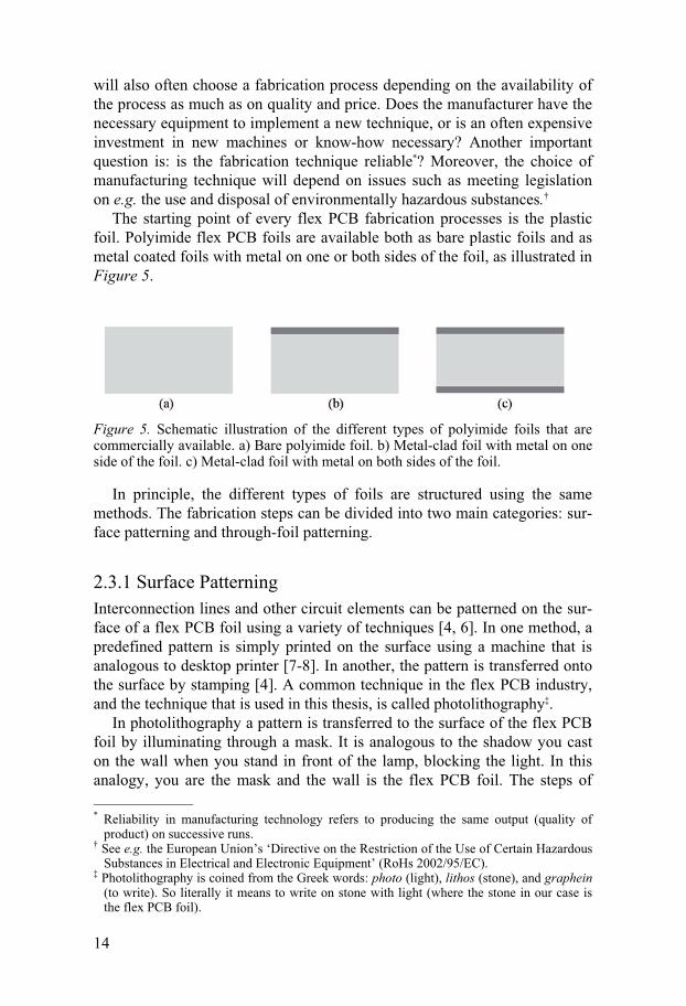
The starting point of every flex PCB fabrication processes is the plastic foil. Polyimide flex PCB foils are available both as bare plastic foils and as metal coated foils with metal on one or both sides of the foil, as illustrated in Figure 5.
Figure 5. Schematic illustration of the different types of polyimide foils that are commercially available. a) Bare polyimide foil. b) Metal-clad foil with metal on one side of the foil. c) Metal-clad foil with metal on both sides of the foil.
In principle, the different types of foils are structured using the same methods. The fabrication steps can be divided into two main categories: sur-face patterning and through-foil patterning.
2.3.1 Surface Patterning Interconnection lines and other circuit elements can be patterned on the sur-face of a flex PCB foil using a variety of techniques [4, 6]. In one method, a predefined pattern is simply printed on the surface using a machine that is analogous to desktop printer [7-8]. In another, the pattern is transferred onto the surface by stamping [4]. A common technique in the flex PCB industry, and the technique that is used in this thesis, is called photolithography‡.
In photolithography a pattern is transferred to the surface of the flex PCB foil by illuminating through a mask. It is analogous to the shadow you cast on the wall when you stand in front of the lamp, blocking the light. In this analogy, you are the mask and the wall is the flex PCB foil. The steps of * Reliability in manufacturing technology refers to producing the same output (quality of
product) on successive runs. † See e.g. the European Union’s ‘Directive on the Restriction of the Use of Certain Hazardous
Substances in Electrical and Electronic Equipment’ (RoHs 2002/95/EC). ‡ Photolithography is coined from the Greek words: photo (light), lithos (stone), and graphein
(to write). So literally it means to write on stone with light (where the stone in our case is the flex PCB foil).
15
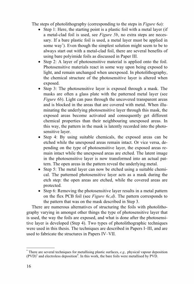
photolithography are illustrated in Figure 6. A more detailed description is found in the following paragraph (and in [1]).
Figure 6. Photolithography. a) The process steps: (1) The starting point – a metal-clad foil. (2) A photosensitive layer is applied. (3) The foil is illuminated through a patterned mask. The illuminated areas in the photosensitive layer become ‘acti-vated’. (4) The photosensitive layer is developed and the illuminated areas are etched away. (5) The exposed metal is etched. (6) The photosensitive layer is re-moved revealing the structured metal. b) A photolithography mask. The light goes through the transparent (open) areas in the mask, and is stopped by the opaque (cov-ered) areas. The image is reproduced with kind permission from FBH/schurian.com. c) A photograph of copper lines on the surface of a polyimide foil. d) A close-up of a copper structure on a polyimide foil (taken by electron microscopy).
16
The steps of photolithography (corresponding to the steps in Figure 6a): � Step 1: Here, the starting point is a plastic foil with a metal layer (if
a metal-clad foil is used, see Figure 5b, no extra steps are neces-sary. If a bare plastic foil is used, a metal layer must be applied in some way*). Even though the simplest solution might seem to be to always start out with a metal-clad foil, there are several benefits of using bare polyimide foils as discussed in Paper III.
� Step 2: A layer of photosensitive material is applied onto the foil. Photosensitive materials react in some way upon being exposed to light, and remain unchanged when unexposed. In photolithography, the chemical structure of the photosensitive layer is altered when exposed.
� Step 3: The photosensitive layer is exposed through a mask. The masks are often a glass plate with the patterned metal layer (see Figure 6b). Light can pass through the uncovered transparent areas and is blocked in the areas that are covered with metal. When illu-minating the underlying photosensitive layer through this mask, the exposed areas become activated and consequently get different chemical properties than their neighbouring unexposed areas. In this way, the pattern in the mask is latently recorded into the photo-sensitive layer.
� Step 4: By using suitable chemicals, the exposed areas can be etched while the unexposed areas remain intact. Or vice versa, de-pending on the type of photosensitive layer, the exposed areas re-main intact while the unexposed areas are etched. The latent image in the photosensitive layer is now transformed into an actual pat-tern. The open areas in the pattern reveal the underlying metal.
� Step 5: The metal layer can now be etched using a suitable chemi-cal. The patterned photosensitive layer acts as a mask during the etch step: the open areas are etched, while the covered areas are protected.
� Step 6: Removing the photosensitive layer results in a metal pattern on the flex PCB foil (see Figure 6c,d). The pattern corresponds to the pattern that was on the mask described in Step 3.
There are numerous alternatives of structuring the foils with photolitho-graphy varying in amongst other things the type of photosensitive layer that is used, the way the foils are exposed, and what is done after the photosensi-tive layer is developed (Step 4). Two types of photolithographic techniques were used in this thesis. The techniques are described in Papers I–III, and are used to fabricate the structures in Papers IV–VII.
* There are several techniques for metallising plastic surfaces, e.g., physical vapour deposition (PVD)1 and electroless deposition9. In this work, the bare foils were metallised by PVD.
17
2.3.2 Through-foil Patterning Entire circuits can be patterned on the surface of a flex PCB using the tech-nique described in the previous section. Such patterns can be sufficient to serve a number of purposes. However, to create more complex structures, it is often necessary to build vertical structures extending through the foil. For example, by creating a hole through the foil and filling it with metal, it is possible to electrically connect a circuit that is on the top side of the foil with a circuit that is on the bottom side (see Figure 7). The resulting structures are three dimensional circuits which are more compact, and in some cases can have new functional possibilities. Such an electrical connection is called a through-hole via interconnect, or in short: a via.
Figure 7.A schematic cross-section of two through-hole via interconnects.
A number of techniques for creating vertical through-foil structures exist in the flex PCB industry*. The first step in producing these structures is cre-ating the actual hole through the foil. When this is done, the hole can be filled entirely or in part with e.g. a metal. The main techniques in the first type of processes is discussed in Section 3.2, while the second type is treated in e.g. [6, 9-12].
The smallest dimensions that are attainable with a via hole fabrication technique are often dependent on the thickness of the foil. Smaller holes are possible in thinner foils. Hence, an important term in describing such a fab-rication technique is the aspect ratio of the resulting holes. The aspect ratio of a structure is the ratio of its height to its width. For example, a circular hole that is 100 μm deep with a diameter of 25 μm has an aspect ratio of 4. The same diameter in a 25 μm thick foil the aspect ratio is only 1. Conse-quently, for a specific height, the higher the aspect ratio the smaller the via hole, and in turn, the larger number of vias that can be packed into a specific area.
* An even larger number of techniques exist (such as deep reactive ion etching), but as the flex PCB industry is highly cost limited, many of these techniques become unsuitable.
18
Drilling There are two types of drilling techniques: mechanical drilling and laser drilling. These techniques are treated in detail in [4, 6]. In the first technique, holes are created by physically removing material from the foil by a me-chanical drill. The pattern of via holes that are to be drilled is predefined and fed to a computer control that moves the drill from location to location. This is why the technique is also called CNC drilling (computer numerical control drilling). Several sheets can be drilled at the same time, and holes with di-ameters down to 50 μm are possible in a 50 μm thick foil (i.e., aspect ratio of 1) [4]. However the technique becomes less productive, in other words slower, with decreasing hole size. Furthermore, the number of sheets that can be drilled at the same time decreases as well.
In the second technique, lasers are used instead of mechanical drills to form the hole. The laser does not mechanically remove the foil material but rather ablates it. In other words it rapidly heats up the material, causing it to evaporate or sublimate. To prevent the surrounding material from heating up as well, the laser light is pulsed quickly (e.g. 109 times a second) at high power peaks. There are a number of different laser systems, each with its advantages and disadvantages. For example, excimer lasers can produce small well-defined holes with diameters down to 10 μm in 25 μm thick foil (i.e. aspect ratio of 2.5) [4]. However, excimer lasers are slow. On the other hand, carbon dioxide lasers are fast but only when creating larger holes (lar-ger than 70 μm). As with mechanical drilling, the ablated pattern is defined by a computer control.
It is important to note that both drilling techniques are sequential, i.e. one hole at a time. This means that the processing costs per hole are the same regardless of the number of holes that are produced, which in turn means that the total cost increases with increasing number of holes per foil.
Chemical and plasma etching Chemically etching through-foil holes refers to removing material from the foil in a predefined area using a chemical. The chemicals that are used can either be in the wet phase, i.e. liquid chemicals, or in the dry phase, i.e. by using a form of gas called plasma.
In both etching techniques the areas that are to be etched are defined us-ing surface patterning techniques such as lithography (see Section 2.3.1). The result is a mask layer, e.g. the metal layer in Figure 6 a, that has open-ings where the holes are to be etched. The mask layer here is analogous to the mask that is used in lithography (see Figure 6a,b). The etchant, i.e. wet or dry, is chosen so as to be selective so that it mainly etches the foil material and not the mask (e.g. the metal layer in Figure 6 a).
19
Figure 8. Mechanisms in chemical and physical etching. (1) Accelerated electrons originating from the plasma ions hit gas molecules that are present in the chamber, causing them to dissociate into reactive species. (2) The reactive species react with molecules on the surface of the foil. (3) The reaction products diffuse away. (4) Some of the plasma ions are accelerated towards the flex PCB foil. (5) Some of the ions collide with reactive species, pushing them forward. These molecules react with surface molecules and diffuse away. (6) Some of the accelerated plasma ions hit the target and knock out molecules from the surface. (7) The knocked out molecules react with some of the reactive species and diffuse away.
In wet etching, the flex PCB is dipped into a container that holds the etchant. The etchant reacts with open areas in the foil, dissolving the foil material. Dry etching is a more complicated process, and is explained in [1] and in the following steps:
� Step 1: The flex PCB foil is placed in a reactor where different gas-ses are introduced.
� Step 2: The gases are activated to form a plasma. A simple explana-tion of plasma is that by applying energy to a gas, for example by heating it or applying an electrical spark, some of the gas molecules lose electrons and become positively charged ions. The freed elec-trons collide with other gas molecules, causing them to lose elec-trons, and so on. The mixture of energetic molecules, ions and elec-trons is a different form of matter called plasma*. Everyday exam-ples of plasma are lightning bolts and neon lamps.
� Step 3: The open areas are etched using one or both of the follow-ing etch processes (see Figure 8):
o Chemical etching: Free electrons originating from the gas molecules that became plasma ions are still present in the chamber. These energetic electrons now hit other gas spe-cies that are present in the chamber causing them to break
* The other forms of matter are: solid, liquid and gaseous. Transforming gas into plasma by applying energy is analogous to transforming water into vapour by boiling it.
20
down into more reactive species (free radicals). For exam-ple, a gas that is commonly used in dry etching, freon (CF4), is dissociated into CF3
+, CF3 and F molecules. The latter molecules are highly reactive and quickly react with molecules that are on the surface of the foil. The resulting combination diffuses (spreads) away from the target.
o Physical etching: The ions are accelerated towards a target, in this case the material to be etched, so that they hit the target. The molecules on the surface are knocked off the surface by the impact.
Chemical etching is fast and isotropic, i.e. the etching rate is the same in
all directions. This means that when etching a hole that is 50 μm deep, the diameter of the hole increases with 100 μm. Physical etching on the other hand is anisotropic, but slow. Combining the two etch processes provides the advantages of both.
The polyimide foils that are used in this thesis are easily etched using chemical and physical plasma etching. The two etch processes can produce through-holes with diameters down to 70 μm in a 50 μm thick foil (i.e. as-pect ratio of 1) [4]. The main advantage of these processes is that they are batch processes and therefore the processing costs do not depend on the number of holes that are etched. This means that processing costs per hole decrease with an increasing number of holes that are produced. So although higher aspect ratios are possible using laser drilling, chemical and plasma etching techniques are more cost advantageous when producing a large amount of holes. However, it should be mentioned that in the case of chemi-cal wet etching, waste treatment and costs related to that are a major issue.
The through-hole fabrication processes that are presented in this thesis were developed as an alternative to conventional chemical and plasma tech-niques. Using the processes in Papers I–III, through-foil structures with higher aspect ratios are possible. In addition, the resultant through-holes enable new applications that are not possible using the conventional tech-niques (demonstrated in Papers IV–VII). The developed processes are dis-cussed in more detail in the following chapter.
21
3. Ion Track Enabled Through-Foil Structures
As mentioned in the previous chapter, the fabrication processes that are pre-sented in this thesis are based on conventional flex PCB techniques. How-ever, the resulting through-foil structures are fundamentally different from their conventional counterparts. Instead of being completely solid or hollow with metal walls, these new structures consist of metal wires that are embed-ded in the flex PCB foil. Multiple wire structures and conventional structures are illustrated in Figure 9. Applications of these structures are discussed in Papers IV–VII and Chapter 4.
Figure 9. Different types of through-foil structures. a) Conventional through-foil structure that is hollow with metallic walls. It has the form of a hole that is fabri-cated with chemical or plasma etching. a) Conventional structure that is completely filled with metal. It has the form of a hole that is fabricated by laser or mechanical drilling. c) High aspect ratio multiple wire structures that are presented in this thesis.
Multiple wire structures are enabled by introducing a pre-treatment step into the conventional fabrication process. Here, the flex PCB foils are pre-treated by irradiation with energetic ions so as to get specific material prop-erties. This irradiation step is an established technique called ion track tech-nology. However, combining ion track technology with flex PCB fabrication techniques is a relatively new concept. This is discussed in more detail in Papers I and III and in this chapter.
22
3.1 Ion Track Technology Energetic ions passing through certain solid materials will damage the mate-rial in its path. If the charged particle has high enough energy, it will leave a continuous channel, only a few nanometres* wide, of transformed material behind it. These channels are called ion tracks. Ion track formation is illus-trated in Figure 10.
Figure 10. Principle of ion track formation. (1) A cross-sectional view of the un-treated material. (2) Energetic ions pass through a material. (3) Each ion that passes through leaves a path of damaged material, called an ion track.
The transformed material in an ion track is different from the pristine ma-terial that surrounds it [13-15]. The different material properties lead to dif-ferent etch rates in certain chemicals. By using the appropriate chemical, the tracks can be etched hundreds, if not thousands, of times faster than the pris-tine material. In other words, in the right etchant, the tracks are opened up long before the surrounding material, forming thin pores through the foil. Once the pores are open, they can be enlarged by etching longer as the pris-tine material is still being etched. Thus, by controlling the etch time, it is possible to control the pore size (see Figure 11). Resulting pores are shown in Figure 12.
Figure 11. Principle of ion track etching. (1) Cross-section view of a material with ion tracks. (2) The material is put in an etchant. The tracks are etched at a higher rate than the surrounding pristine material. (3) After a while in the etchant, the tracks are completely etched, forming continuous pores through the material. The pristine material is still being etched, slowly. (4) If etching is continued, the surroundings continue to be etched, enlarging the pores.
* A nanometre is a thousandth of a micrometre (i.e., a billionth of a metre).
23
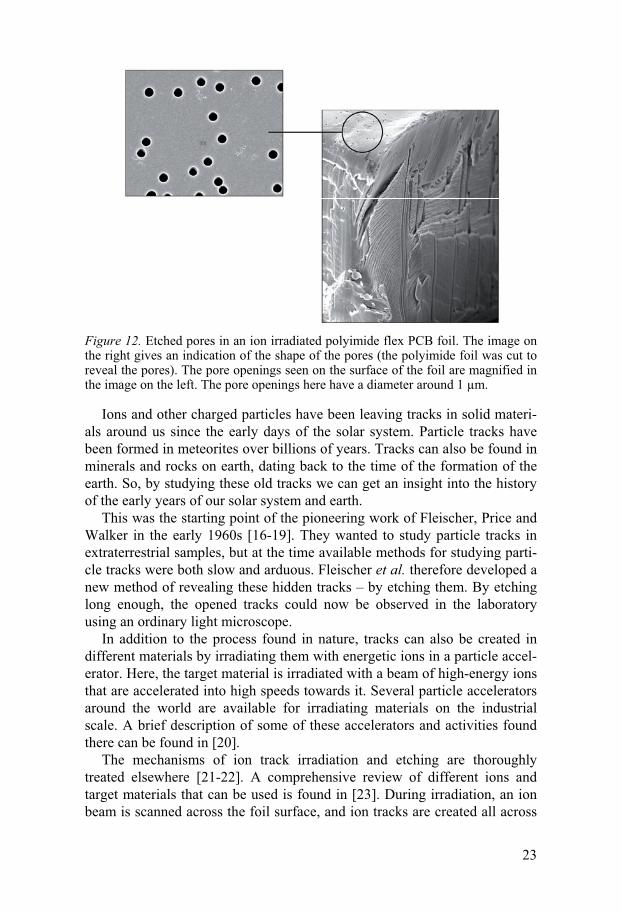
Figure 12. Etched pores in an ion irradiated polyimide flex PCB foil. The image on the right gives an indication of the shape of the pores (the polyimide foil was cut to reveal the pores). The pore openings seen on the surface of the foil are magnified in the image on the left. The pore openings here have a diameter around 1 μm.
Ions and other charged particles have been leaving tracks in solid materi-als around us since the early days of the solar system. Particle tracks have been formed in meteorites over billions of years. Tracks can also be found in minerals and rocks on earth, dating back to the time of the formation of the earth. So, by studying these old tracks we can get an insight into the history of the early years of our solar system and earth.
This was the starting point of the pioneering work of Fleischer, Price and Walker in the early 1960s [16-19]. They wanted to study particle tracks in extraterrestrial samples, but at the time available methods for studying parti-cle tracks were both slow and arduous. Fleischer et al. therefore developed a new method of revealing these hidden tracks – by etching them. By etching long enough, the opened tracks could now be observed in the laboratory using an ordinary light microscope.
In addition to the process found in nature, tracks can also be created in different materials by irradiating them with energetic ions in a particle accel-erator. Here, the target material is irradiated with a beam of high-energy ions that are accelerated into high speeds towards it. Several particle accelerators around the world are available for irradiating materials on the industrial scale. A brief description of some of these accelerators and activities found there can be found in [20].
The mechanisms of ion track irradiation and etching are thoroughly treated elsewhere [21-22]. A comprehensive review of different ions and target materials that can be used is found in [23]. During irradiation, an ion beam is scanned across the foil surface, and ion tracks are created all across
24
the surface of the foil. Hence, if the foils are not masked in some way, pores will also be opened up everywhere during the etching step. Alternatively, instead of irradiating the whole surface of the foil, it is possible to move the ion beam (or the sample) in a predefined pattern. A number of such ion beam ‘direct write’ techniques have been developed [24-26], but as they are all time-consuming and expensive, they are not beneficial for large-scale large-area production. In this case, it is more cost-efficient to scan the beam over the whole surface of foils and mask them in some way (either during or after irradiation). Different techniques of masking the foil are discussed in Papers I, III, IV and in Section 3.3.
Porous ion track etched plastic foils are commercially used in several ap-plications such as water filtration. Here the water is flowed through the po-rous foil. Particles that are larger than the pores are blocked and do not pass through the filter. Since the size of the pores in the ion track etched mem-brane can be controlled, the size of the particles that are to be blocked can also be controlled. An overview of the different applications of ion track etched membranes can be found in [27].
Porous ion track membranes and foils are also used in different fields of research. For example, in life sciences the membranes are used as e.g. scaf-folds for cultivating and studying cells [28-29]. The porous membranes are also used as templates for depositing and studying the physics of nanometre- sized structures [30-34]. Depositing such structures in porous foils is dis-cussed in the following section.
An important term in describing ion track etched foils is porosity. Here, porosity is the ratio of the area of all the pores in the foil material to the area of the whole foil. In other words, the term describes how much of the foil’s surface has actually been etched away. Porosity is defined by the number of pores in an area, i.e., the pore density, and the size of the etched pores. The porosity of the foils can be varied to fulfil different demands. For example, in the case of filtration, one might want a large number of pores so that the water can easily flow through the filter. At the same time, the pores should be relatively small so that larger particles can be filtered away. In cell culti-vation however, many relatively large pores are more beneficial. Two differ-ent porosities are shown in Figure 13.
The pore density is controlled during the irradiation step. Each ion that passes through the foil leaves one track behind it. Therefore, by controlling the irradiation dose, the number of ion tracks can be regulated. The irradia-tion dose can be adjusted between just one ion per foil up to billions of ions per square centimetre. The foils in this thesis were irradiated with doses be-tween 5 million and 500 million ions per square centimetre. The size of the pores can be defined by how long the foils are etched (see Figure 11). In this thesis, foil porosities lie between 0.1 % and 17 %. Different issues on the choice of foil porosity are discussed in Papers I, III, IV and VI.
25
Figure 13. Two different porosities: 3 % and 17 %. The surface area is identical in the two images. In the left image there are around 70 million pores per square cen-timetre. In the right image there are around 500 million pores in the same area.
3.2 Deposition in Porous Ion Track Foils A large number of different materials can be deposited in porous ion track
foils. Different metals [35-37], alloys [38], semiconductors [39-40] and plas-tic materials [41-42] have been deposited. The structures can either be solid or hollow, depending on the deposition method (see Figure 14). In addition to being used in science to study the physics of nanometre-sized objects, the deposited structures are envisaged to be used in a range of technological applications such as flat panel displays (as field emitters) [43-44], wireless communication (in tuneable filters and circulators) [45-46], and sensors [47-49]. An overview of possible applications of structures deposited in porous ion track foils can be found in [50].
Figure 14. Deposited structures in porous ion track foils. a) Solid nickel wires with diameters around 0.15 μm. b) Hollow copper tubes with diameters around 10 μm.
The structures that are deposited in the porous foils in this thesis are all metallic and solid, and we refer to them as wires or strands. Their shape is similar to the wires in Figure 14a, and they are deposited by electrodeposi-tion (also known as electroplating). The wires can be seen as replicas of the pores they are deposited in. The number and diameter of the deposited wires depend on the porosity of the foil.
26
In electrodepostion, a metal* is deposited onto the surface of an object. The process involves placing the object into a solution that contains ions of the metal to be coated. An electric current is then passed through the system which causes the metal ions in the solution to pick up electrons at the surface of the object and adhere there as metal ions. Electrodeposition is illustrated schematically in Figure 15.
Figure 15. Illustration of electrodeposition. The surface to be deposited upon is called a working electrode. The electrode is put in a solution called an electrolyte which contains ions of the metal that is to be deposited. When an electrical potential is applied, the metal ions are attracted to the electrode and if the conditions are right, they will adhere to the surface. The potential is applied between the working elec-trode and a counter electrode which is also in the solution (not shown). To be able to do so, the electrodes must be electrically conducting.
Electrodeposition is described extensively elsewhere [9, 51]. The mecha-
nisms and fundamentals of electrodeposition are beyond the scope of this text. However, a brief description of how the technique is used in this thesis for depositing structures in porous foils can be found in Figure 16 and in Paper I. Typical deposited structures are shown in Figure 17.
Figure 16. Main steps of depositing structures in ion track porous foils. (1) Cross-sectional view of a porous foil. (2) A metal layer is deposited onto one side of the foil to make it conducting. The deposited metal layer is then covered on the backside with a non-conducting protective layer. In this way, deposition is restricted to the bottom of the pores. (3) The foil is put in an electrolyte, and a current is applied between it and a counter electrode. Metal is deposited in the pores forming wires. (4) If deposition is continued, the wires fill the pores completely and start to grow on the surface.
* Other materials can also be deposited by electrodeposition, such as semiconductors and conductive polymers.
27
All the vertical through-foil structures that are presented in this thesis consist of multiples of wires like those shown in Figure 17. The fabrication processes that are presented all begin with irradiating polyimide flex PCB foils with energetic ions, followed by the etching and electrodeposition tech-niques described in this chapter. However, to be able to fabricate the struc-tures in this thesis, the aforementioned steps must be combined with other patterning techniques. This is discussed in more detail in Paper III and in the next section.
Figure 17. Nickel wires electrodeposited in porous polyimide foils. After deposition the foil was removed by plasma etching to reveal the wires. a) Wires that are around 20 μm long and have diameters around 0.2 μm. Deposition was stopped before the wires reached the surface of the foil. b) Top view of a wire showing its cross section. Electrodeposition was stopped before the wire reached the surface. The wire diame-ter is around 0.5 μm. c) Here, deposition was continued after the pores were filled. The spherical ‘caps’ on the top of the wire are formed when the wires grow onto the surface of the foil. The wire diameters are around 0.2 μm.
28
3.3 Ion Track Lithography As mentioned in Section 3.2, ion tracks are created all across the surface of the foil. This means that when etched, if the foils are not masked or pat-terned in some way, pores will be opened up everywhere. Hence, during the electrodeposition step, wires will be deposited everywhere in the foil (again, if the foils are not masked in some way during deposition).
To be able to etch tracks and or deposit wires only in certain areas, the foils must be masked in some way. This can be done during irradiation, dur-ing track etching or during electrodeposition. The collective name for these masking techniques is ion track lithography. A number of different such techniques have been presented, three of which were developed in this the-sis. Ion track lithography techniques are discussed in Papers I–III and in the following sections.
3.3.1 Masking during Irradiation The ions have a certain penetration depth into the material that is irradiated. This penetration depth depends on the ion that is used, its energy and on the material that is irradiated [21-23]. Therefore, if a masking layer of some material with a certain thickness is placed in front of the target, the ions can be stopped in this layer before reaching the target material underneath*. Now, if this masking layer has openings in it, the ions will be able to pass through these openings and create tracks in the material below. This is analogous to photolithography where the light is blocked by the metal layer in the glass mask (see Section 2.3.1). In this way, a relief of the pattern in the masking layer is projected onto the foil, and this type of techniques is there-fore called ion track projection lithography. Two masking techniques are illustrated in Figure 18.
Figure 18. Ion track projection lithography techniques. a) A stencil mask placed in front of the target. Here, the ions are stopped before they reach the target. b) A masking structure (could also be a patterned layer) is placed on the target.
* Depending on the type of material in the masking layer and its thickness, the ions can either be stopped completely, or slowed down so that their range is limited to a certain depth.
29
A number of structures fabricated using ion track projection techniques have been presented such as miniaturised quartz tuning forks [52] and mag-nets [53] for use in microelectronics. An advantage of ion track projection lithography is that no additional masking steps are necessary to etch and or deposit wires in certain areas. Furthermore, if the pores are etched until they merge, ion track projection lithography can be used as an alternative tech-nique for micromachining deep vertical structures [54]. A further advantage is that by using nanostructured masks, it is possible to create nanometre-sized vertical structures without using direct-write techniques [55-56].
3.3.2 Masking after Irradiation A disadvantage of ion track projection lithography is that only the pro-
jected mask structures can be fabricated in the materials that are irradiated. If a material is irradiated through a mask in the form of a cross, it will not be possible to etch tracks in a circle (without irradiating again). This in turn means that the irradiated materials can only be used in a limited number of pre-designated applications. Furthermore, the size of the irradiated areas is often limited to the area of the mask.
If ion track lithography is to be used as a large-scale commercial structur-ing technique, masking should be performed in the subsequent steps. In this way, the end users, e.g. a flex PCB manufacturer, will not need to have ac-cess to irradiation facilities but may use pre-irradiated (and sometimes pre-etched and metallised) foils. Furthermore, larger areas can be irradiated us-ing continuous roll-to-roll irradiation facilities which can significantly lower the process costs. Here, the ion beam is scanned across the surface of the foil which is moving. Several commercial facilities are being used today to manufacture plastic porous membranes (e.g. Nucleopore®) by large-scale roll-to-roll irradiation and wet etching.
There are in principle four ion track lithography techniques on homoge-nously irradiated foils. Three of the techniques are presented in this thesis (Papers I-III), whereas the fourth is presented in [57]. The three processes presented in this thesis are illustrated in Figure 19. The resulting through-foil structures consist of multiple submicrometer sized metallic wires.
The metal content of the multiple wire structures is determined by the number and size of the wires that constitute it. This, in turn, is defined by the porosity of the foil as each wire corresponds to one pore. By varying the metal content of the structures, it is possible to adjust their overall properties. For example, a low metal content structure has high electrical resistance and low thermal conductivity, and vice versa. This means that the properties of the structures can be modified to adapt them to different applications. This feature, and other advantages of using multiple wires through-foil structures, are discussed in Papers I, III, IV and VI and in the following chapter.
30
Figure 19. Process steps in the ion track lithography techniques presented in this thesis. a) Process in Paper I. (1) The starting point of the process is a foil that is irradiated homogeneously to a specific depth. (2) Lithographically defined apertures are dry etched into the layer of unirradiated material (3) Pores are etched throughout the whole foil. Only the pores in the dry etched apertures are open from both sides. (4) A metal layer is deposited on back side of foil. (5) Wires are deposited in the open pores. The wires merge and fill the bottom of the dry etched apertures. (6) Lithography to interconnect the structures. b) Process in Paper II. (1) Starting point is an irradiated and wet etched foil. (2) A metal layer is deposited onto one side of the foil. A dry photoresist film is laminated on the opposite side of the foil. Aper-tures are lithographically defined in the resist layer. (5) Wires are deposited in the exposed pores. The wires merge and fill the apertures. (6) Interconnection lithogra-phy. c) Process in Paper III. (1) Starting point is an irradiated, wet etched and metal-lised foil. (2) Lithographically defined apertures are dry etched down uncovering the wires. (6) Interconnection lithography.
31
4. Summary of the Work Presented in the Included Papers
The publications presented in this thesis deal with how ion track lithography has been further developed and used for fabricating high aspect ratio struc-tures in flex PCBs. In the following sections, a background for each paper is presented, describing why the work was done. A summary of the main re-sults and conclusions is presented for each paper. The publications can be divided into two main categories: fabrication processes and demonstrated applications.
4.1 Fabrication Processes 4.1.1 Paper I In this paper, a process is presented for fabricating high aspect ratio multiple wire structures in a polyimide flex PCB foil.
Background As mentioned in Chapter 2, wet etching is one of the most cost-efficient techniques for creating a large number of through-foil structures in flex PCBs. However, the aspect ratios that are attainable using conventional wet etch techniques are low compared to other techniques such as laser drilling*. Therefore, to get the same lateral dimensions as with other techniques, wet etched structures must be created in thinner foils.
Flex PCB foils with thicknesses down to 3 μm are commercially available and can be processed. However, foils that are that thin have drawbacks for use in a number of applications†, and are not as mechanically robust as thicker ones (e.g. 25 μm and thicker). Therefore, new wet etching techniques that can produce high aspect ratio through-foil structures are of interest.
Ion track lithography has been suggested as such a technique [57]. Through-foil structures with aspect ratios up to 2 have been demonstrated in * Aspect ratios up to 1 are attainable with conventional wet etch techniques, and up to 5 with laser drilling. The reader is reminded that higher aspect ratios lead to higher possible packing densities, i.e. a larger amount of structures can be packed into the same area. † Such as in high frequency Radio Frequency Microelectromechanical Systems (RF-MEMS) due to capacitive coupling [57].
32
a polyimide flex PCB foil. However, due to the type of foil that is used, as-pect ratios over 2 are not attainable. Furthermore, it is not possible to fabri-cate multiple wire structures with a low metal content (see Section 3.3) in that material, which in turn limits the possible applications of the resulting structures.
The process that is presented in Paper I was developed in a different flex PCB foil material to enable wet etched structures with higher aspect ratios, as well as with lower metal content, than what was previously presented [2].
Results A new ion track lithography process was successfully demonstrated for bare polyimide foils. The fabrication process allows for through-foil structures with higher aspect ratios, higher packing densities and lower metal contents than previously presented wet etch techniques. A schematic of the process is shown in Figure 19a. Resulting through-hole vias are shown in Figure 20.
Figure 20. Through-foil structures fabricated using the process presented in Paper I. a) Top view of a via opening before metallisation. Pores openings can be seen in the aperture. Each group of pores constitutes a through-foil structure. b) A group of wires that constitutes a multiple wire structure. The wires merged when they reached the bottom surface of the via aperture. The polyimide was removed by plasma etch-ing. Residues remain and can be seen around the via).
Square vias with a side length down to 26 μm were demonstrated in a 75 μm thick foil, corresponding to an aspect ratio of 3. Both low and high via metal contents (0.1 % and 10 %, respectively) can be fabricated using the technique. In turn, it can be concluded that the fabrication technique can be used to fabricate both high-resistive vias for use in e.g. sensor applications, and low-resistive vias for use in e.g. RF-MEMS (Radio Frequency Micro-electromechanical Systems).
Electrical measurements on both low and high metal content vias show that the vias are electrically reliable. Furthermore, it was shown that the vias can withstand current densities up to 4 ·106 A/cm2 per wire in the via.
33
4.1.2 Paper II The fabrication process presented in Paper II was developed as a simpler and more cost-efficient alternative to the process presented in Paper I.
Background A common motivation for all the fabrication processes presented in this the-sis is to achieve compatibility with fabrication techniques that are commonly used in the flex PCB industry today. In this way, the processes can become viable fabrication technologies.
The process presented in Paper I was developed as a step towards that goal. However, an important parameter in that process is that it requires a precise control of the penetration depth of the ions into the foil. This necessi-tates either restrictions on the irradiation parameters which may be expen-sive to achieve, or using a mask layer during irradiation which again may raise process costs. Therefore, even though the process in Paper I can be used to produce high aspect ratio structures, it may prove to be too compli-cated to implement in flex PCB fabrication at a larger scale. Hence, new ion track lithography techniques that overcome these restrictions are of interest.
The idea in this paper was that the starting point for the end user, e.g. a flex PCB manufacturer, is a foil that is already etched with pores every-where. In this case, irradiation and etching can be seen as material pre-treatment steps that can be performed by the material supplier, and all the end user then needs to do is to use flex PCB manufacturing techniques to fabricate vertical structures in the porous foil.
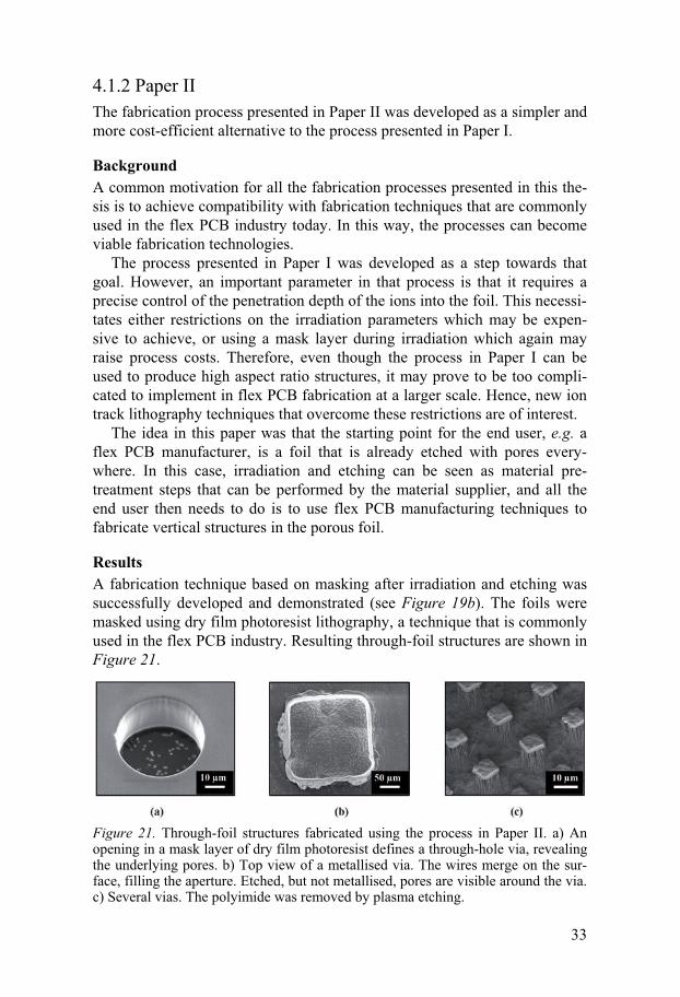
Results A fabrication technique based on masking after irradiation and etching was successfully developed and demonstrated (see Figure 19b). The foils were masked using dry film photoresist lithography, a technique that is commonly used in the flex PCB industry. Resulting through-foil structures are shown in Figure 21.
Figure 21. Through-foil structures fabricated using the process in Paper II. a) An opening in a mask layer of dry film photoresist defines a through-hole via, revealing the underlying pores. b) Top view of a metallised via. The wires merge on the sur-face, filling the aperture. Etched, but not metallised, pores are visible around the via. c) Several vias. The polyimide was removed by plasma etching.
34
Square vias with a side length down to 22 μm that had a pitch (centre-to-centre distance) of 40 μm were opened up in a 75 μm thick polyimide foil. However, it proved difficult to metallise these vias in a uniform and reliable way. This means that if these small dimensions are required, the electrode-position step should be further developed, or alternatively another, thinner dry resist laminate should be used as the masking step.
The smallest vias we were able to metallise uniformly had a side length of 32 μm and a pitch of 60 μm. The vias had a metal content of 0.4 %, but in principle, the process could be used for fabricating structures with the same metal contents as the vias presented in Paper I. Electrical measurements show that the vias are electrically reliable.
4.1.3 Paper III The fabrication process in Paper III was developed to decrease the number of fabrication steps for the end user of the process, and in that way simplify the fabrication process. Furthermore, a review and comparison of ion track lithography techniques is included in the paper.
Background As mentioned before, the objective of the work presented in this thesis is to develop processes that can become viable flex PCB fabrication techniques. The idea in Paper III was to further simplify the process in Paper II for the end user by including the through-foil metallisation step in the material pre-treatment steps. In this way, the number of steps that remain for the end user to fabricate through-foil structures is decreased, potentially decreasing proc-ess lead times and costs.
Results A fabrication technique where through-foil structures are defined after met-allisation of the whole foil was demonstrated (see Figure 19c). Resulting structures are shown in Figure 22.
The demonstrated through-hole vias had a side length of 65 μm. It should however be possible to fabricate smaller vias as the lowest attainable dimen-sions are limited by the resolution of the photolithography and plasma etch-ing steps. The electrical reliability of the vias was not characterised.
The review of ion track lithography shows that the presented techniques all have their inherent advantages and disadvantages. It was also shown that ion track lithography techniques based on irradiating the whole surface of the foil may potentially become commercially viable techniques. However, due to limitations in the availability of irradiation facilities it was found that the techniques are, for the time being, only of interest for niche applications.
35
Figure 22. Through-foil structures fabricated using the process in Paper III. a) Top view of part of a metallised structure. Pores that were not metallised all the way up can be seen in the upper right corner. b) A through-hole via. Wires that are not part of the via can be seen around the structure. The polyimide was removed by plasma etching. Some residues remain and can be seen on the top of the surrounding wires.
4.2 Applications 1: Vertical Thermopiles To understand what a thermopile is, it is important to understand the
thermoelectric effect. The thermoelectric effect (see Figure 23) occurs when two different conductors are connected at two junctions. If the junctions are at different temperatures, hot and cold, an electric potential (voltage) will be generated. The larger the temperature difference between the two junctions, the higher the voltage is generated. A pair of such conductors is called a thermocouple, and a chain of thermocouples is called a thermopile.
Figure 23. The thermoelectric effect. An electrical potential is generated when two different conductors, i.e. a thermocouple, are connected at two junctions, and these two junctions are at different temperatures.
36
To paraphrase, a thermocouple converts the difference in temperature be-tween its two junctions into an electric voltage. This potential can either be used to measure that temperature difference, like a thermometer, or it can be used as a source of energy, like a battery. If designed differently, the ther-mocouples can also operate in the reverse direction, i.e. they can convert an electric potential to heat. In this way, the thermocouples can be used as cool-ing and heating devices, called Peltier elements.
The electrical potential that is generated from a thermocouple depends on the thermopower of the two conductors. The thermopower of a material, also called its Seebeck coefficient, is a measure of the thermoelectric voltage that is generated in response to a temperature difference. To get a large potential, it is beneficial to choose two conductors that have a large difference in ther-mopower, i.e. a large relative Seebeck coefficient.
For example, copper and nickel have Seebeck coefficients of +7 μV/K and -15 μV/K, respectively [59]. This corresponds to a relative Seebeck co-efficient of 22 μV/K. Now, by replacing copper and nickel with antimony and bismuth that have Seebeck coefficients of +47 μV/K and -70 μV/K [59], the relative Seebeck coefficient becomes 117 μV/K, and the voltage gener-ated becomes significantly higher for the same temperature difference.
It should be noted that the voltage generated also depends on other mate-rial properties such as resistivity and heat conductivity. Furthermore, factors such as device design, fabrication methods and the intended application play a role in the choice of the two thermocouple materials.
By connecting two thermocouples together, the potential generated is doubled, and by connecting ten, the potential becomes ten times as much, and so on. Therefore, thermocouples are connected in series, forming a thermopile, and the larger the number of thermocouples in a thermopile, the higher the voltage generated.
Thermopiles are used in a range of applications. For example, the tem-perature inside a refrigerator is often regulated using thermocouples, and many electronic devices are cooled using Peltier elements. Thermopiles are also widely used in different microsystems where they function as local cooling points [60-61], energy scavengers* and power generators [62-64] and temperature and radiation sensing elements in different applications [65-68].
Commercial miniaturized thermopiles are fabricated on rigid substrates such as silicon using high thermopower, but expensive materials. Thermo-piles on flexible substrates have therefore received interest as they are light-weight, bendable and can be used on non-planar surfaces [69-73].
* Energy scavenging, also known as energy harvesting, is the process of collecting and storing energy surrounding us. Wristwatches that are driven by your body temperature, but also windmills and solar cells, are examples of energy scavenging.
37
4.2.1 Paper IV In this paper, vertical thermopiles are demonstrated and characterized in a polyimide flex PCB foil. Background Conventional thermopiles in MEMS have a planar design with the ther-molegs (the two different conductors) going between a hot and cold spot on the surface. An important advantage of using such a planar design is that a whole range of high thermopower materials can be deposited onto the sur-face, and structured into micrometre sized thin lines. In this way, thermo-piles that generate a large electrical potential can be fabricated using conven-tional thin film techniques. However, in this case, both the materials and fabrication methods are relatively costly.
In a vertical design, the hot and cold spots are on the opposite side of the substrate, see Figure 24, and the thermolegs go up and down between the two surfaces of the substrate. Here, the entire surfaces can be used as either the hot or cold surface, which means that the whole substrate can be used for the thermocouples. Furthermore, the thermocouples can be packed closer together in a vertical design in comparison with the planar one. This in turn means that a larger number of thermocouples can be packed into the same area, and hence, higher electrical voltages can be generated. That being said, the challenge here lies in fabricating vertical structures with the same ther-moelectric performance as their planar thin film counterparts. Although a few papers have been presented on vertical thermopiles [74-77], only quasi-vertical structures have been previously achieved in flex PCB foils [78].
Figure 24. Vertical thermopiles with their hot and cold junctions on opposite sides of the foil.
As mentioned before, the voltage generated depends on the difference in temperature. It is therefore important to achieve as large a temperature gra-dient across the thermopiles as possible. Metallised through-foil structures that are fabricated using conventional flex PCB methods have high metal
38
contents, and they therefore conduct heat well. This means that a tempera-ture difference between the two surfaces of the foil will be quickly evened out*, and the voltage generated will decrease or vanish.
The idea in Paper IV was to reduce the metallic content of the vertical structures by using multiple wire structures. In this way, the overall heat conductance of the vias is reduced, and a heat gradient can be maintained across the vertical thermocouples.
Results The process presented in Paper I was further developed to allow for the deposition of two different metals (nickel and antimony) in alternating vias (see Figure 25). Thermopiles with up to 180 nickel-antimony thermocouples were fabricated and connected in series to form thermopiles in a 75 μm thick polyimide foil, shown in Figure 25. 540 thermocouples were fabricated on the same 22 x 22 mm2 sample. The thermopiles showed a clear and reliable voltage response to a temperature gradient that was applied across the foil thickness. The response was measured to be 24 μV/K.
Figure 25. Top view of the polyimide foil. Each via consists of four subvias. a) After deposition of antimony and nickel wires in alternating vias. The opposite of the foil is structured into an electrode pattern that allows for the deposition of two different metals through the foil (in two steps). This pattern can be seen through the transparent polyimide foil. b) The antimony and nickel thermolegs are connected in series forming a thermopile.
The measured thermopile voltage response was a factor 3 lower than what was calculated from the material parameters [59]. Four main reasons for this discrepancy are presented and discussed in the paper. Furthermore, it is dis-cussed how the thermopile structures and the fabrication process can be de-veloped to improve this voltage response. The main factors are treated in the Paper V and in the following section.
* Unless the top and bottom surfaces are actively heated or cooled.
39
4.2.2 Paper V The multiple wire thermopile structures presented in Paper IV are further developed to improve their voltage response. The thermopiles are character-ized for use in infrared (IR) radiation sensing elements.
Background As mentioned before, the measured thermopile voltage response in Paper IV was lower than what was calculated from tabulated values. A source of this discrepancy is the actual length of the antimony thermoleg in the thermo-piles. Nickel plugs were electrodeposited both at the top and bottom of the antimony wires to protect the antimony wires and the copper layer at the bottom of the pores from corrosion. Consequently, the length of the anti-mony part of the wires was smaller than the full wire length, in fact only around 46 μm. This in turn means that the temperature difference across the antimony part of the wire (which is the temperature difference generating the voltage) is smaller than that across the whole thickness of the foil. Hence, by increasing the length of the antimony in the wires, a larger portion of the applied temperature gradient is available for generating the thermoelectric voltage. The idea in Paper V was to do this by increasing the total length of the wires, i.e. increasing the thickness of the foil from 75 μm to 125 μm.
Furthermore, it was hypothesized in Paper IV that improvements in the thermopile fabrication process with regards to electrodeposition uniformity could potentially improve the voltage response. The idea in Paper V was therefore to replace the patterned seed layer electrodes used in Paper IV (see Figure 25a) with an unstructured metal layer. This can be done by using the process presented in Paper II and developing it to allow for the deposition of two different metals in alternating vias.
A further motivation for the work presented in Paper V was to demon-strate the vertical thermopiles as infrared (IR) radiation sensing elements which are a common application area for miniaturized thermopiles [79].
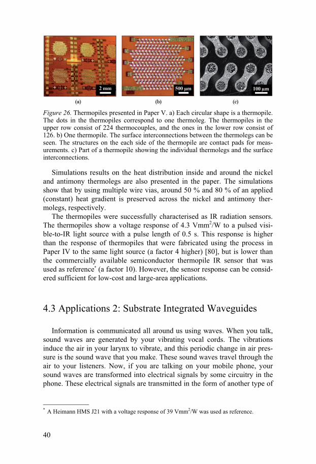
Results The process presented in Paper II was developed to allow for the deposition of nickel and antimony in alternating vias. The process was also optimized for larger sample areas and for depositing wires in thicker polyimide foils (125 μm). Resultant thermopiles are shown in Figure 26.
Thermopiles with up to 224 thermocouples were successfully demon-strated. The length of the antimony centre in the thermocouples was in-creased to around 115 μm in the thicker foils. 50 thermopiles holding more than 4500 thermocouples were fabricated on the same 45 x 45 mm2 sample. Furthermore, the number of thermocouples per unit area (i.e., the packing density) was increased compared to the structures in Paper IV.
40
Figure 26. Thermopiles presented in Paper V. a) Each circular shape is a thermopile. The dots in the thermopiles correspond to one thermoleg. The thermopiles in the upper row consist of 224 thermocouples, and the ones in the lower row consist of 126. b) One thermopile. The surface interconnections between the thermolegs can be seen. The structures on the each side of the thermopile are contact pads for meas-urements. c) Part of a thermopile showing the individual thermolegs and the surface interconnections.
Simulations results on the heat distribution inside and around the nickel and antimony thermolegs are also presented in the paper. The simulations show that by using multiple wire vias, around 50 % and 80 % of an applied (constant) heat gradient is preserved across the nickel and antimony ther-molegs, respectively.
The thermopiles were successfully characterised as IR radiation sensors. The thermopiles show a voltage response of 4.3 Vmm2/W to a pulsed visi-ble-to-IR light source with a pulse length of 0.5 s. This response is higher than the response of thermopiles that were fabricated using the process in Paper IV to the same light source (a factor 4 higher) [80], but is lower than the commercially available semiconductor thermopile IR sensor that was used as reference* (a factor 10). However, the sensor response can be consid-ered sufficient for low-cost and large-area applications.
4.3 Applications 2: Substrate Integrated Waveguides Information is communicated all around us using waves. When you talk,
sound waves are generated by your vibrating vocal cords. The vibrations induce the air in your larynx to vibrate, and this periodic change in air pres-sure is the sound wave that you make. These sound waves travel through the air to your listeners. Now, if you are talking on your mobile phone, your sound waves are transformed into electrical signals by some circuitry in the phone. These electrical signals are transmitted in the form of another type of
* A Heimann HMS J21 with a voltage response of 39 Vmm2/W was used as reference.
41
waves, electromagnetic waves, through the antenna on the phone, via a base station, to your listener’s phone.
Electromagnetic waves can be seen as a combination of oscillating mag-netic and electric fields travelling through space at the speed of light. Elec-tromagnetic waves are classified into different categories according to their frequency*, ranging from short wavelength high-energy gamma and x-ray waves to long wavelength radio (RF) waves. The latter category of waves is used in a whole range of devices, for example, wireless technologies of all kinds, from remote control toys to mobile phones and wireless internet, send or receive RF waves.
Radio waves can be made to carry information by systematically chang-ing a combination of the wave frequency, amplitude, or phase within a fre-quency band. The width of this frequency band determines how much in-formation can be sent at the same time, i.e. the communication speed. Wire-less communication technology today is moving towards broader band-widths, as an increasing amount of functions are required to be integrated and used in the same device. By moving the frequency band to higher fre-quencies, broader bands are possible.
A consequence of higher operation frequencies is that the size of compo-nents in RF devices must be decreased. This is an important driving force for miniaturisation [82]. Further advantages are that the RF devices can become lighter and cheaper, with increased performance and with a larger number of functions integrated into the same volume [83]. Moreover, the miniaturised components have low power consumption [84]. Hence, a large number of micromachined RF components are being developed in both industry and academia [85-87].
4.3.1 Paper VI In Paper VI, a new concept for substrate integrated waveguides (SIW) is demonstrated in a flex PCB foil for high frequency applications.
Background RF signals are transmitted from one position to another using antennas or waveguides. An antenna radiates the RF waves out in space. Depending on the application, the antenna can be designed to radiate equally in all direc-tions or to radiate in one preferred direction. In waveguides, the wave is confined to an area along its propagation path. Here, radiation is a negative phenomenon as it is desirable to transmit the full signal power from one point to another. To achieve this, waveguides are often closed, that is, like a pipe. If the pipes are hollow with metallic walls, the wave is efficiently con-
* Definitions of the wave parameters (frequency, wavelength, amplitude, phase and polarisa-tion) can be found in [81
42
fined. However, such structures are rigid which is not always desirable. Fur-thermore, when fabricating miniaturised waveguides, such metallic hollow structures are expensive to fabricate. Hence, alternative types of micro-machined waveguides have been developed to overcome these restrictions [88]. However, none of these structures can match the performance of the aforementioned metallic pipes.
A new concept for microfabricated waveguides called substrate integrated waveguides (SIW) has recently been introduced [89]. SIWs can be seen as rectangular waveguides that are incorporated into the substrate itself. It con-sists of two vertical walls, a top and a bottom layer, with a dielectric material in between (the substrate). In this way, the SIWs can also be seen as pipe-like, but with the additional merits of miniaturisation and ease of integration with other RF components on the same substrate. Several SIWs have been demonstrated for use in a number of different RF components at frequencies ranging from around 10 GHz to 180 GHz [90-94]. It should be noted here that the SIWs that showed high performance at the higher frequencies were fabricated using relatively costly fabrication techniques and materials.
SIWs can be manufactured using rigid PCB fabrication processes to re-duce fabrication costs. In this case, the vertical walls of the SIWs are not continuous metallic walls, but rather rows of metallised through-hole vias. This is due to process limitations; the via holes are drilled through substrates that are usually several hundred micrometres thick and if they are drilled too closely, the substrate will become mechanically unstable. As there are gaps between the vias, some of the power that is transmitted in the wave radiates out of the waveguide and is lost. This leakage loss is frequency dependent, and the higher the frequency the higher the losses. Consequently, SIWs fab-ricated by PCB fabrication processes can not operate at high frequencies. Previously presented SIWs fabricated with PCB processes have been dem-onstrated at frequencies up to 28 GHz [95].
The idea in Paper VI was to substitute the rows of vias with multiple wire structures. Since the wires and the spacing between them can be reduced to a few hundred nanometres, the walls can be seen as continuous metallic walls. Hence, the leakage losses of the waveguide were expected to become negli-gible, and higher operation frequencies become possible.
Results SIWs with multiple wire vertical walls were fabricated in a porous polyimide flex PCB foil using the process presented in Paper II. Two sample batches were fabricated. In the first batch, the relative permittivity and loss tangent of the porous polyimide foils were characterised in the frequency range of 70 GHz to 90 GHz as ion track porous foils had not been previously charac-terised or used at such high frequencies. Two foil porosities were examined: 3 % and 17 %, and it was found that the lower porosity foils have higher performance in that frequency range. In addition, the insertion losses of mul-
43
tiple wire vias with metal contents of 3 % and 17 % were characterised in the same frequency range. The measured material parameters were then used to design optimised SIWs in the second fabrication batch. The SIWs were de-signed for the 77 – 81 GHz frequency band*. Microstrip lines, grounding vias and a SIW-based antenna were also fabricated in this batch. The antenna was fabricated as a demonstrator of the SIW concept. The foils in the second batch had a porosity of 3 %. Resulting structures are shown in Figure 27.
Figure 27. Structures from the second fabrication batch in Paper VI. a) Segment of a SIW wall. The SIW is detached from the underlying copper layer. The polyimide was removed by plasma etching. b) Multiple wire through-hole vias for grounding. Part of a microstrip line can also be seen. The polyimide was removed here. c) Top view of an SIW-based slot antenna and grounding vias.
The SIW concept was successfully demonstrated at 79 GHz. This allows for several SIW-based devices using PCB fabrication processes foils at higher frequencies than previously presented. Since the leakage losses are significantly reduced, the SIWs are expected to function at even higher fre-quencies. In principle, the operation frequency will not be limited by the leakage losses from the SIW walls, but rather the dielectric losses of the substrate. The performance of the SIW and the SIW-based antenna was found to be in good agreement with simulations.
4.3.2 Paper VII In this paper, SIW-based antennas and antenna arrays are demonstrated and characterised at 79 GHz.
Background In Paper VI, an SIW-based single slot antenna was demonstrated and partly characterised at 79 GHz. The performance of the antenna was found to be promising for applications where flexible light-weight antennas are desir-able. The idea in Paper VII was therefore to further investigate the use of SIWs with multiple wire walls in antennas and antenna arrays.
* The 77– 81 GHz band has been designated by the European Commission for short range radars in automobiles for features such as collision warning and blind spot monitoring [96].
44
In Paper VI, it was seen that the leakage losses from the SIW were re-duced and the operation frequency could be increased to at least 79 GHz. However, the actual losses were not modelled or calculated. A further moti-vation for the work presented in Paper VII was therefore to achieve a better understanding of the loss characteristics of the SIW walls.
Results SIW-based longitudinal and four-by-four slot array antennas were success-fully demonstrated in a flex PCB foil at 79 GHz. In addition, the SIW-based single slot antenna presented in Paper VI was further characterised. A slot antenna arrays are shown in Figure 28.
Figure 28. SIW-based slot array antennas presented in Paper VII. The slots are all of equal length (1.4 mm) and are offset from the centre of the SIW. a) Longitudinal slot array antenna. b) Four-by-four slot array antenna showing the feeding network. c) Four-by-four slot array antenna. The antenna is bent to show its flexibility.
The measured port impedance and radiation patterns of the demonstrated antennas show that they have favourable radiation characteristics with suffi-cient impedance bandwidth at 79 GHz. The measured results are in agree-ment with their simulated values. Calculations of the loss characteristics of the SIW walls confirmed that dielectric losses of the substrate dominate. It is therefore believed that the antenna performance can be improved by trans-ferring the SIW fabrication processes to a lower-loss dielectric material.
4.4 Achieved Goals As discussed in Chapter 1, a main goal in this thesis was to build structures that exhibit increased performance. In this thesis, increased performance is defined as adding new functional possibilities and or improving existing features. Further main goals in this thesis were miniaturisation and building
45
flexible structures. The fabrication processes and structures presented in this thesis all fulfil one or more of these goals, as described below:
� The fabrication process in Paper I allows for creating multiple wire structures in a polyimide flex PCB foil. By changing the substrate material and the fabrication process, the structures are further miniaturised and lower metal-contents are possible. In this way, the structures themselves are improved allowing for new applications. An example of such an application is presented in Paper IV.
� The process presented in Paper II allows for fabrication of multiple wire vias in a simpler and more industrially compatible way. The new possibility in this paper is not the structures themselves (the degree of miniaturisation here is actually decreased), but is rather the fabrication process itself. As it is more industrially compatible, it has a higher potential in becoming a commercially viable tech-nique – which can be seen an important improvement.
� In Paper III, the processes in Papers I–II and [57] are discussed and compared. Furthermore, a new process for fabricating multiple wire vias is presented. The increased performance of this process is that it is a step further in simplifying the process for use in the flex PCB industry. A few applications that can be enabled with this new process are also discussed in the paper.
� Paper IV deals with an application that is enabled by the fabrication processes described above. The new feature that is presented is ver-tical thermopiles in flex PCB foils, allowing for new application ar-eas. The improved feature that is presented is a further development of the technique in Paper I to enable build more complex structures.
� In Paper V, the improved feature is the thermopiles’ higher voltage response to IR light (compared to the thermopiles in Paper IV). Furthermore, the fabrication process is simpler and more industri-ally compatible (the process is a development of the process in Pa-per III). Hence, it can be seen that the vertical thermopiles have po-tential as commercially viable components in low cost and large area applications.
� The new concept of SIWs that is presented in Paper VI leads to a clear improvement in the performance of the waveguides and an SIW-based antenna. In this paper, the improved feature is that the leakage losses of SIWs fabricated by PCB processes are minimised; whereas the new possibility is that the SIWs can be used at signifi-cantly higher frequencies enabling new application areas for flex PCB components. Furthermore, the process in this paper leads to miniaturisation of the vertical walls in the SIWs.
� In paper VII, the new features that are demonstrated are more ad-vanced SIW-based antenna array designs in a flex PCB at high fre-quencies.
46
5. Conclusive Remarks
The work presented in this thesis shows that ion track lithography techniques can become viable alternatives to conventional flex PCB wet etching tech-niques. The resulting multiple wire structures are superior to their conven-tional counterparts when it comes to their higher aspect ratios, higher possi-ble packing densities and low metallic cross-section. Furthermore, metallised through-foil structures with larger areas and more complicated geometries are possible without losing the mechanical stability of the foil. This in turn enables applications that are not possible using conventional techniques and structures.
However, implementing ion track lithography in a commercial flex PCB fabrication facility faces a number of challenges. First, the fabrication proc-esses have not been demonstrated for large-area processing. The bottleneck of these processes lies in the metallisation step which I believe must be fur-ther developed for larger areas and higher deposition rates. Second, multiple wire vias have relatively high resistive losses compared to conventional structures. I therefore believe the fabrication processes must be further de-veloped to allow for higher metal contents and for deposition of metals with lower resistivity, such as copper. Third, access to irradiation facilities today is limited. This in turn limits the supply of material for flex PCB production on a larger-scale. And finally, fabricating structures in thinner dielectric foils may remove the need for high aspect ratio and high packing densities. If the thinner foils can be structured using more mature techniques, I believe flex PCB manufacturing facilities will be reluctant to adopt a new technique. However, I believe multiple wire vias still be interesting for use in niche applications like those demonstrated in this thesis.
47
Sammanfattning på svenska
Miniatyrisering, flexibelt och ökad prestanda är några nyckelbegrepp som kan beskriva målet med denna avhandling. Allt arbete som presenteras här går ut på att utveckla lösningar som har med dessa nyckelbegrepp att göra.
Miniatyrisering, att göra saker mindre, är en viktig drivkraft i båda forsk-ningsvärlden och i industrin. Man miniatyriserar för att få plats med mer på samma yta, och med fler strukturer kan man få fler funktioner. Dessutom kan man också få nya funktioner som inte är möjliga i större skala. Vidare så betyder det ofta också att det blir billigare och bättre. Strukturerna som pre-senteras i denna avhandling är i mikrometerskala, det vill säga, i storleksord-ningen från några tusendels millimeter till några tiondedels millimeter.
Det andra nyckelbegreppet, flexibelt, är inkluderat för att alla strukturer i denna avhandling använder tunna plastfolier som byggsten. Dessa folier kallas flexibla kretskort och används i många i olika applikationer. Man väl-jer ofta att bygga saker i flexibla kretskort för att de är små och tunna, väger lite och kan böjas i olika former. Detta är viktiga parametrar i användnings-områden där vikt och storlek måste begränsas, som till exempel inne i en hörapparat, eller i en apparat med böjbara delar, som till exempel en vikbar mobiltelefon. Den typ av flexibelt kretskortsmaterial som användes i denna avhandling heter polyimid, och är utvalt för dess utmärkta elektriska, meka-niska och kemiska egenskaper.
Det sista nyckelbegreppet, ökad prestanda, betyder i denna avhandling an-tigen att möjliggöra nya funktioner eller att förbättra existerande enheter.
Arbetet som presenteras i avhandlingen kan delas i två huvudkategorier. Den första kategorin består av nya sätt att bygga mikrometerstora strukturer i tunna folier. Där presenteras tre olika sätt att göra detta, alla med sina förde-lar och nackdelar. Det de alla har gemensamt är att de börjar med att folierna beskjuts med tunga snabba joner för att möjliggöra att man ska kunna göra tunna raka porer genom folien.
När dessa tunga snabba joner passerar genom en plast eller andra icke elektriskt ledande material lämnar de spår av förändrat material efter sig. Dessa spår kallas jonspår. Eftersom materialet i jonspåren är olikt den om-kringliggande ursprungliga plasten kan de etsas på olika sätt. Om en lämplig etsvätska används kan man möjliggöra att jonspåren etsas tusentals gånger snabbare än resten av materialet. På det sättet kan jonspåren etsas upp till långa tunna kanaler som kallas porer. Sådana porer visas i Figur 1. När po-rerna är etsade, kan man börja fylla de med exempelvis metall. På det sättet
48
kan man deponera långa tunna trådar som kan användas inom en mängd olika användningsområden. Byggsätten som utvecklas och används i denna avhandling handlar om att bygga strukturer som består av buntar av sådana trådar som visas i Figur 2. Detta görs genom att kombinera jonbestrålning och etsning av jonspår med andra mer konventionella tekniker som används för att strukturera flexibla kretskort.
Figur 1. Porer i en plastfolie. Här har plasten blivit klippt för att visa porerna. Bilden till höger visar långa och tunna porer. Bilden till vänster visar poröppningar på ytan av plastfolien. Pordiametern på ytan är runt en mikrometer och porernas längd är runt 50 mikrometer.
Figur 2. Trådbunt-strukturer. Här har den omkringliggande plasten etsats bort för att visa trådarna. Strukturerna blev byggda med metoderna som presenteras i a) Artikel I. b) Artikel II och c) Artikel III. I alla bilder har trådarna vuxit ihop på det som var plastytan.
49
Genom att variera antalet trådar i bunten och storleken på trådarna, kan man variera mängden metall i trådbunten. På det viset kan man variera tråd-buntens egenskaper. Om man exempelvis har få och tunna trådar kan man få strukturer med låg elektrisk- och värmeledningsförmåga, och vice versa. Detta betyder att man kan skräddarsy strukturernas egenskaper för att anpas-sa dom till olika applikationer.
Den andra kategorin handlar om två olika tillämpningar som möjliggörs genom att använda trådbuntar. I den första bör man ha så lite metall som möjligt, i den andra vill man ha så mycket som möjligt.
Den första tillämpningen som presenteras är termostaplar (kallas också termostackar) i flexibla kretskort. Termostaplar baseras på den termoelekt-riska effekten som kan förklaras på följande vis: När två elektriska ledare är sammankopplade på två olika ställen, genereras det en elektrisk spänning om de två kopplingställena inte har samma temperatur. Ett sådant par ledare kallas ett termopar och en serie termopar utgör en termostapel. Spänningen som genereras i termostapeln beror på vilka material som används, tempera-turskillnaden och på hur många termopar som finns i termopelaren.
Termoparen i kommersiella miniatyriserade termostaplar brukar bestå av tunna linjer metall på en yta. Materialen som används brukar vara optimera-de för att ge en hög spänning, men dom är ofta dyra. För att få plats med flera termopar på en yta och samtidigt sänka kostnaderna kan man gå över till en vertikal design där termoparen går upp och ner genom plasten. Här genereras spänningen av en temperaturskillnad mellan ovan- och undersidan av folien. Problemet här är att om man vill göra detta i ett tunt flexibelt kretskort och termoparledarna är solida, så utjämnas temperaturskillnaden omedelbart och ingen spänning kan genereras. Detta förklaras med att de solida strukturerna har för hög värmeledningsförmåga för att kunna behålla en temperaturskillnad. En lösning på problemet är att minska mängden me-tall i termoparledarna och att på det sättet minska värmeledningsförmågan. Detta kan göras genom att använda ledare som består av tunna metalliska trådar – med andra ord de tidigare nämnda trådbuntarna. Detta visar vi i Ar-tikel IV där vi demonstrerade vertikala termostaplar i ett flexibelt kretskort (polyimid). I artikel V förbättrade vi strukturerna och visade att de vertikala termostaplarna kan används för att mäta temperaturen beröringsfritt via dess värmestrålning.
Det andra tillämpningsområdet som presenteras är vågledare och anten-ner. Dessa strukturer används i enheter som utnyttjar radiovågor för att skicka eller ta emot information, som till exempel mobiltelefoner eller tråd-lösa Internetnätverk. Här skickas information genom att systematisk ändra vågens egenskaper inom ett frekvensband. Bredden av det frekvensbandet bestämmer hur mycket information som kan överföras samtidigt, det vill säga hur snabbt man kan kommunicera. Genom att flytta frekvensbandet till högre frekvenser kan man få ett bredare frekvensband, och därmed en snab-
50
bare kommunikation. En följd av att arbeta vid högre frekvenser är att stor-leken på alla strukturer måste minskas ner till mikrometerskala.
Vågledare och antenner används för att transportera vågorna från ett ställe till ett annat. Antennen strålar vågor ut till omgivningen, medan vågledaren är som ett rör som leder vågen längs en bana. Om röret är ihåligt och väg-garna är gjorda av metall, kan hela vågen ledas fram utan förluster. Vid till-verkningen av sådana effektiva metalliska rör i mikrometerskala används dyra material och tillverkningsmetoder. Dessutom är de materialen som an-vänds rigida, vilket inte alltid är önskvärt. Därför har flera alternativa vågle-dare blivit utvecklade, men ingen med samma prestanda som de metalliska rören.
I papper VI introducerar vi ett nytt koncept för att tillverka relativt billiga och flexibla metalliska rör som fortfarande kan fungera som effektiva vågle-dare vid höga frekvenser. Här blir väggarna i röret en skog av många och tätpackade trådar (täta trådbuntar). Om trådarna är tillräckligt tätpackade fungerar skogen som en metallisk vägg, och vågledaren fungerar som ett metallisk rör. Detta visas i artikel VI och i artikel VII demonstreras olika antenner som är byggda på detta sätt.
51
Acknowledgments
Takk Jan-Åke og Klas for at jeg fikk begynne som doktorand her på denne fantastiske avdelingen. Nå som boken er klar kan jeg innrømme at jeg trodde mikrostrukturer betydde bcc og fcc, men dette ble helt klart mye bedre. Og videre takk til Klas for all støtte, entusiasme, åpenhet og tillit (og for at du faktisk sier ja til ’team building’-forslag som reiser til Polen og julebord på herregård). Takk Micke for alt jeg har lært av deg og for et morsomt og stimulerende samarbeid. Vi må vel være opp i noen tusen timer ren labtid? Og takk for at du alltid har vært tilgjenglig for hjelp, diskusjoner og tankevekkere. Thank you, Henrik and Shi for a great collaboration. It has been fun! And a special thank you for all the extra hours you put in at the end even though you were so busy yourselves. I really appreciate it. Takk Greger for uunnværlig hjelp med mine manuskript. Jeg er nesten tilbøyelig til å begynne å vurdere å gå med på dine STIM-krav. Vi får se. Takk Carin, Caroline, Anja, Ingrid, Ewa og Agneta for all hjelp gjennom årene. Og Jonatan for datahjelp. Og MSL for support i labben. Og til Dubbelsture for at den ikke døde. Men ikke takk til Edwards og sånn er det. Takk Wikipedia for all min kunnskap. En stor takk til alle mine mikmek-venner, past and present. Takk for all hjelp og støtte på veien og for en fantastisk tid på reiser og seminarer og klokkan-fem-macka-fika, for ikke å glemme på Loehmanns og hotelljakt i Lyon. Takk tribologer og andre Ångan-venner for good times både på og utenfor the big Å.
52
Takk Sune for all hjelp med referanser. Takk Linda og Sara for korr-lesing. Thank you, Mary for emergency editing support. Og tack Anders för hjälp med min svenska sammanfattning. Og takk till Sølvi for den norske delen av min svenske sammenfatning, og for heiarop og sangtimer og alt imellom. Og takk til Geir for at du er min Uppsala-bastion. Og sist men ikke minst, takk til mine andre bastioner: Mz and Pz, Tarek, Nadya, Hassan, Amina og Anchooga (in advance), og mine kjære venner. Shoukran alla! Hanna
53
References
1. M J Madou (2002) Fundamentals of Microfabrication: the Science of Miniaturi-zation 2nd ed. (Boca Raton: CRC Press LLC) 1 – 69, 134 – 144
2. K Gilleo (2003) The Circuit Centennial Circuitree Retrieved at circuitree.com: www.circuitree.com/CDA/Articles/Web_Only_Editorial/dc439de37efe7010VgnVCM100000f932a8c0 (retrieved 25/01/2008).
3. printed circuit board The American Heritage® Science Dictionary. Retrieved 30/01/2008 from dictionary.com: dictionary.reference.com/browse/printed cir-cuit board (retrieved 30/01/2008)
5. J M Yang, J Bell, Y Huang, M Tirado, D Thomas, A H Forster, R W Haigis, P D Swanson, R B Wallace, B Martinsons and M Krihak (2002) An integrated, stacked microlaboratory for biological agent detection with DNA and immuno-assays Biosensors and Bioelectronics 17(6-7) 605 – 618
6. Coombs C F Jr (2002) Printed Circuits Handbook 5th ed. (New York: McGraw-Hill) 28.5 – 31.14, 58.1 – 58.17
7. J G V Scott (2005) Digital printing for printed circuit boards Circuit World 31(4), 34 – 41
8. T Sutter (2005) An overview of digital printing for advanced interconnect appli-cations Circuit World 31(3) 4 – 9
9. M Schlesinger and M Paunovic (2000) Modern Electroplating 4th ed. (New York: Wiley) 1–200, 645–666, 759–762, 769–790,
10. N Patton (2005) Flexible PCBs and plating through holes: challenges and solu-tions CircuiTree, 18(9) 44, 46, 48, 50
11. G Allardyce, M Lefebvre , H Tsuchida , M Kusaka and S Hayashi (2004) Cop-per electroplating technology for microvia filling CircuiTree 17 24–34
12. M Lefebvre, G Allardyce, M Seita, H Tsuchida, M Kusaka, and S Hayashi (2003) Copper electroplating technology for microvia filling Circuit World 29(2) 9 – 14
13. A Chapiro (1988) Chemical modifications in irradiated polymers Nuclear In-struments & Methods in Physics Research, Section B: Beam Interactions with Materials and Atoms 32(1–4) 111–114
14. L Calcagno, G Compagnini and G Foti (1992) Structural modification of poly-mer films by ion irradiation Nuclear Instruments & Methods in Physics Re-search, Section B: Beam Interactions with Materials and Atoms 65(1–4) 413– 422
15. E Balanzat, N Betz and S Bouffard (1994) Swift heavy ion modification of polymers Nuclear Instruments & Methods in Physics Research, Section B: Beam Interactions with Materials and Atoms 105(1–4) 46–54
16. R L Fleischer, P B Price and R M Walker (1963) Tracks of charged particles in high polymers Science 140 1221 – 1222
54
17. R L Fleischer, P B Price and E M Symes (1964) Novel filter for biological ma-terials Science 143 249 – 250
18. R L Fleischer, P B Price and R M Walker (1964) Track registration in various solid-state nuclear track detectors Physical Review 133(5A) A1443–A1449
19. R L Fleischer, P B Price and R M Walker (1965) Tracks of Charged Particles in Solids Science 149 383 – 393
20. P Apel (2003) Swift ion effects in polymers: Industrial applications, Nuclear Instruments and Methods in Physics Research, Section B: Beam Interactions with Materials and Atoms 208(1–4) 11–20
21. R L Fleischer, P B Price and R M Walker (1975) Nuclear Tracks in Solids (Berkeley: University of California Press) 3 – 118
22. R Spohr (1990) Ion Tracks and Microtechnology. Basic Principles and Applica-tions (Wiesbaden: Vieweg & Sohn Verlag) 1–262
23. B E Fischer and R Spohr (1983). Production and use of nuclear tracks: imprint-ing structure on solids Reviews of Modern Physics 55(4) 907 – 948
24. B E Fischer and S Metzger (2000) Single-ion micromechanics MRS Bulletin 25 (2) 39–42
25. S Reyntjens and R Puers (2001) A review of focused ion beam applications in microsystem technology Journal of Micromechanics and Microengineering 11(4) 287–300
26. A Persaud, J A Liddle, T Schenkel, J Bokor, T Ivanov and I W Rangelow (2005) Ion implantation with scanning probe alignment Journal of Vacuum Sci-ence and Technology B: Microelectronics and Nanometer Structures 23(6) 2798–2800
27. P Apel (2001) Track etching technique in membrane technology Radiation Measurements 34(1–6) 559–566
28. T Sergent-Engelen, C Halleux, E Ferain, H Hanot, R Legras and Y-J Schneider (1990) Improved cultivation of polarized animal cells on culture inserts with new transparent polyethylene terephthalate or polycarbonate microporous mem-branes Biotechnology Techniques 4(2) 89–94
29. S Zibek, A Stett, P Koltay, M Hu, R Zengerle, W Nisch and M Stelzle, (2007) Localized functional chemical stimulation of TE 671 cells cultured on nanopor-ous membrane by calcein and acetylcholine Biophysical Journal, 92(1) 4–6
30. L Gravier, S Serrano-Guisan, J-P Ansermet (2005) Spin-dependent Peltier effect in Co/Cu multilayer nanowires Journal of Applied Physics 97(10) 10C501
31. L Gravier, J-E Wegrowe, T Wade, A Fabian, J-P Ansermet (2002) Ther-mopower and GMR of a single Co-Cu multilayer nanowire IEEE Transactions on Magnetics, 38(5) 2700–2702
32. A Fabian, C Terrier, S S Guisan, P Guittienne, L Gravier and J-P Ansermet (2006) Current-induced magnetization switching in pseudo spin-valves Journal of Physics Condensed Matter 18(5) 1569–1576
33. J. Spiegel, J. de la Torre, M. Darques, L. Piraux, I. Huynen (2007) Permittivity model for ferromagnetic nanowired substrates IEEE Microwave and Wireless Components Letters 17(7) 492–494
34. L Vila, P Vincent, L Dauginet-De Pra, G Pirio, E Minoux, L Gangloff,, S De-moustier-Champagne, N Sarazin, E Ferain, R Legras, L Piraux and P Legagneux (2007) Growth and field-emission properties of vertically aligned cobalt nano-wire arrays Nano Letters 4(3) 521–524
35. J Vetter and R Spohr (1993) Application of ion track membranes for preparation of metallic microstructures Nuclear Instruments and Methods in Physics Re-search Section B: Beam Interactions with Materials and Atoms 79(1-4) 691–694
55
36. C Schonenberger, B M I van der Zande, L G J Fokkink, M Henny, C Schmid, M Kruger, A Bachtold, R Huber, H Birk and U Staufer (1997) Template synthesis of nanowires in porous polycarbonate membranes: electrochemistry and mor-phology Journal of Physical Chemistry B 101(28) 5497–5505
37. M Motoyama, Y Fukunaka, T Sakka, Y H Ogata and S Kikuchi (2005) Electro-chemical processing of Cu and Ni nanowire arrays Journal of Electroanalytical. Chemistry 584(2) 84–91
38. W Ensinger and P Vater (2005) Diameter distributions of metallic nanowires formed by galvanic deposition inside polymer matrix pores Material Science Engineering C 25(5–8) 609–613
39. M Sima, I Enculescu, T Visan, R Spohr and C Trautmann (2004) Electrochemi-cal deposition of PbSe1�xTex nanorod arrays using ion track etched membranes as template Molecular Crystals and Liquid Crystals 418 749–755
40. S Chakarvarti, V Kumar V and S Kumar (2005) Galvanic-fabrication of CdS microstructures using nuclear track filter membranes Journal of Material Sci-ence 40(2) 503–504
41. C G J Koopal, M C Feiters, R J M Nolte, B de Ruiter and R B M Schasfoort (1992) Glucose sensor utilizing polypyrrole incorporated in track-etch mem-branes as the mediator Biosensors & Bioelectronics 7(7) 461–471
42. M-C Clochard, C Baudin, N Betz, A Le Moel, C Bittencourt, L Houssiau, J-J Pireaux and D Caldemaison (2006) New sulfonated pyrrole and pyrrole 3-carboxylic acid copolymer membranes via track-etched templates Reactive and Functional Polymers 66(11) 1296–1305
43. T E Felter, R G Musket and A F Bernhardt (2005) Field emitter arrays and dis-plays produced by ion tracking lithography Nuclear Instruments and Methods in Physics Research, Section B: Beam Interactions with Materials and Atoms 241 (1–4) 346–350
44. A F Bernhardt, R J Contolini, A F Jankowski, V Liberman, J D Morse, R G Musket, R Barton, J Macaulay and C Spindt (2000) Arrays of field emission cathode structures with sub-300 nm gates Journal of Vacuum Science and Tech-nology B: Microelectronics and Nanometer Structures 18(3) 1212–1215
45. A Saib and I Huynen (2006) Periodic metamaterials combining ferromagnetic nanowires and dielectric structures for planar circuits applications", Electro-magnetics 26(3-4) 261–277
46. A Saib, M Darques, L Piraux, D Vanhoenacker-Janvier and I Huynen (2005) Unbiased microwave circulator based on ferromagnetic nanowires arrays of tun-able magnetization state Journal of Physics D (Applied Physics) 38(16) 2759–2763
47. I Enculescu, M E Toimil-Molares, C Zet, M Daub, L Westerberg, R Neumann and R Spohr (2007) Current perpendicular to plane single-nanowire GMR sen-sor Applied Physics A (Materials Science Processing) A86(1) 43–47
48. M Lindeberg and K Hjort (2003) Interconnected nanowire clusters in polyimide for flexible circuits and magnetic sensing applications Sensors and Actuators A (Physical) A105(2) 150–61
49. D Fink, L T Chadderton, K Hoppe, W R Fahrner, A Chandra and A Kiv (2007) Swift-heavy ion track electronics (SITE) Nuclear Instruments and Methods in Physics Research, Section B: Beam Interactions with Materials and Atoms 261 (1–2) 727–730
50. P B Price (2005) Science and technology with nuclear tracks in solids Radiation Measurements 40(2–6) 146-159
51. C H Hamann, A Hamnett and W Vielstich (2007) Electrochemistry (Weinheim: Wiley VCH) 1–338
56
52. G Thornell, H Rapp and K Hjort (2000) X-cut miniature tuning forks realized by ion track lithography IEEE Transactions on Ultrasonics, Ferroelectrics and Frequency Control 47(1) 8–15
53. D Fink, P S Alegaonkar, A V Petrov, M Wilhelm, P Szimkowiak, M Behar, D Sinha, W R Fahrner, K Hoppe and L T Chadderton (2005) High energy ion beam irradiation of polymers for electronic applications Nuclear Instruments & Methods in Physics Research, Section B: Beam Interactions with Materials and Atoms 236(1–4) 11–20
54. G Thornell, R Spohr, E J van Veldhuizen and K Hjort (1998) Micromachining by ion track lithography Sensors and Actuators, A: Physical 73(1– 2) 176–183
55. R Sanz, J Jensen, A Johansson, M Skupinski, G Possnert, M Boman, M Her-nandez-Velez, M Vazquez and K Hjort (2007) Well-ordered nanopore arrays in rutile TiO2 single crystals by swift heavy ion-beam lithography Nanotechnology 18(30) 305303
56. M Skupinski, J Jensen, A Johansson, G Possnert, M Boman, K Hjort and A Razpet (2007) Nanopattern transfer to Si O2 by ion track lithography and highly selective HF vapor etching Journal of Vacuum Science and Technology B: Mi-croelectronics and Nanometer Structures, 25(3) 862–867
57. M Lindeberg and K Hjort (2004) A comprehensive study of ion track enabled high aspect ratio microstructures in flexible circuit boards Microsystem Tech-nologies 10(8-9) 608 – 621
58. W Veit, H Diestel and R Pregla (1990) Coupling of crossed planar multiconduc-tor systems IEEE Transactions on Microwave Theory and Techniques 38(3) 265–269
59. C Nordlin and J ôsterman Physics Handbook for Science and Engineering (1996) 5th ed. (Lund: Studentlitteratur) 45–46
60. H Bottner (2005) Micropelt miniaturized thermoelectric devices: Small size, high cooling power densities, short response time Proceedings 24th Interna-tional Conference on Thermoelectrics (ICT '05), Clemson, SC, USA 1–8
61. V Semenyuk (2006) Miniature Thermoelectric Modules with Increased Cooling Power Proceedings. 25th Interntional Conference on Thermoelectrics (ICT '06), Vienna, Austria 322–326
62. M A Schmidt (2003) Portable MEMS power sources Digest of Technical Papers IEEE International Solid State Circuits Conference 385, 394–395
63. J A Paradiso and T Starner (2005) Energy scavenging for mobile and wireless electronics IEEE Pervasive Computing 4(1) 18–27
64. E Cantatore and M Ouwerkerk (2006) Energy scavenging and power manage-ment in networks of autonomous microsensors Microelectronics Journal 37(12) 1584–1590
65. G Kaltsas and A G Nassiopoulou (1999) Novel C-MOS compatible monolithic silicon gas flow sensor with porous silicon thermal isolation Sensors and Actua-tors A (Physical) 76(1–3) 133–138
66. H L Hartnagel, K Mutamba, J Pfeiffer, R Riemenschneider and J Peerlings, (1999) MEMS based on III-V-compounds for sensing applications and optical communication Proceedings 57th Annual Device Research Conference Digest (DRC), Santa Barbara, CA, USA 112–115.
67. R Buchner, C Sosna, M Maiwald, W Benecke and W Lang (2006) A high-temperature thermopile fabrication process for thermal flow sensors Sensors and Actuators A (Physical) 130–131 262–266
68. M Hirota, Y Nakajima, M Saito, F Satou and M Uchiyama (2004) Thermoelec-tric infrared imaging sensors for automotive applications Proceedings of SPIE - 5359 111–125
57
69. W Qu, M Plotner W-J Fischer (2001) Microfabrication of thermoelectric gen-erators on flexible foil substrates as a power source for autonomous microsys-tems Journal of Micromechanics and Microengineering 11(2) 146–152
70. J Weber, K Potje-Kamloth, F Haase, P Detemple, F Volklein and T Doll (2006) Coin-size coiled-up polymer foil thermoelectric power generator for wearable electronics Sensors and Actuators, A: Physical 32(1) 325–330
71. N Sato and M Takeda (2005) Fabrication and evaluation of a flexible thermoe-lectric device using metal thin films Proceedings 24th International Conference on Thermoelectrics (ICT'05), Clemson, SC, USA 160–163
72. V Jovanovic and S Ghamaty (2006) Design, fabrication and testing of energy-harvesting thermoelectric generator Smart Structures and Materials 2006 - Smart Structures and Integrated Systems, San Diego, CA, USA 61730
73. M Al khalfioui, A Michez, A Giani, A Boyer and A Foucaran (2003) Ane-mometer based on Seebeck effect Sensors and Actuators A (Physical) 107(1) 36–41
74. G J Snyder, J R Lim, C-K Huang and J-P Fleurial (2003) Thermoelectric micro-device fabricated by a MEMS-like electrochemical process Nature Materials 2(8) 528–531
75. H Bottner, J Nurnus, A Gavrikov, G Kuhner, M Jagle, C Kunzel, D Eberhard, G Plescher, A Schubert and K-H Schlereth (2004) New thermoelectric compo-nents using microsystems technologies Journal of Microelectromechanical Sys-tems 13(3) 414–420
76. W Wang, F Jia, Q Huang and J Zhang (2005) A new type of low power ther-moelectric micro-generator fabricated by nanowire array thermoelectric material Microelectronic Engineering 77(3/4) pp. 223–229
77. W Glatz, S Muntwyler and C Hierold (2006) Optimization and fabrication of thick flexible polymer based micro thermoelectric generator Sensors and Actua-tors A (Physical) 132(1) 337–345
78. K Itoigawa, H Ueno, M Shiozaki, T Toriyama and S Sugiyama (2005) Fabrica-tion of flexible thermopile generator Journal of Micromechanics and Microen-gineering 15(9) 233–238
79. A Graf, M Arndt, M Sauer and G Gerlach (2007) Review of micromachined thermopiles for infrared detection Measurement Science and Technology, 18(7) 59–75
80. M Lindeberg, H Yousef, H Rodjegard, H Martin and K. Hjort (2007) Flexible PCB Vertical Thermopile IR Sensor Proceedings Solid-State Sensors, Actuators and Microsystems Conference (TRANSDUCERS), Lyon, France 2275–2278
81. H D Young and R A Freedman (2000) University physics 10th ed. (San Fran-sisco: Addison-Wesley) 593–613, 1025–1048
82. K J Vinoy, P K Sharma, K A Jose, V K Varadan, V V and Varadan, V. V (2001) Micromachined systems for RF and microwave antenna applications Proceedings of SPIE 4334 156–163
83. H C Kim and K Chun (2007) RF MEMS technology IEEJ Transactions on Electrical and Electronic Engineering 2(3) 249–261
84. L P B Katehi, J F Harvey and E Brown (2002) MEMS and Si micromachined circuits for high-frequency applications IEEE Transactions on Microwave The-ory and Techniques 50(3) 858–866
85. P Gammel, G Fischer and J Bouchard (2005) RF MEMS and NEMS technol-ogy, devices and applications Bell Labs Technical Journal 10(3) 29–59
86. S Lucyszyn (2004) Review of radio frequency microelectromechanical systems technology IEE Proceedings Science, Measurement and Technology 151(2) 93–103
58
87. J Bouchaud and H Wicht (2005) RF MEMS: Status of the industry and road-maps Proceedings of SPIE 5717 50–54
88. I Llamas-Garro and A Corona-Chavez (2006) Micromachined transmission lines for millimeter-wave applications 16th IEEE International Conference on Electronics, Communications and Computers, Puebla, Mexico 15–20
89. D. Deslandes and K Wu (2001) Integrated microstrip and rectangular waveguide in planar form IEEE Microwave and Wireless Components Letters 11(2) 68–70
90. W Hong, B Liu, G Q Luo, Q H Lai, J F Xu, Z C Hao, F F He and X X Yin (2007) Integrated microwave and millimeter wave antennas based on SIW and HMSIW technology Conference Proceedings IEEE International Workshop on Antenna Technology, Small Smart Antennas Metamaterials Applications 69–72
91. W D'Orazio and K. Wu, "Substrate-integrated-waveguide circulators suitable for millimeter-wave integration IEEE Transactions on Microwave Theory 54(10) 3675–3680
92. Z-C Hao, W Hong, X-P Chen, J-X Chen and K Wu (2005) A single-layer folded Substrate Integrated Waveguide (SIW) filter Proceedings Asia-Pacific Micro-wave Conference 1606279
93. K K Samanta, D Stephens and I D Robertson (2006) 60 GHz multi-chip-module receiver with substrate integrated waveguide antenna and filter Electronics Let-ters 42(12) 701–702
94. D Stephens, P R Young and I D Robertson (2005) Design and characterization of 180 GHz filters in photoimageable thick-film technology IEEE MTT-S Inter-national Microwave Symposium Digest 451–454
95. D Deslandes and K Wu (2003) Millimeter-Wave Substrate Integrated Waveguide Filters Canadian Conference on Electrical and Computer Engineer-ing 1917– 1920
96. The European Commission decision (ECC2006/DEC(04)03) is available online at the European Union’s Internet site: http://eurlex.europa.eu/LexUriServ/ Lex-UriServ.do?uri=CELEX:32004D0545:EN:HTML (last accessed 29/02/08).
Acta Universitatis UpsaliensisDigital Comprehensive Summaries of Uppsala Dissertationsfrom the Faculty of Science and Technology 407
Editor: The Dean of the Faculty of Science and Technology
A doctoral dissertation from the Faculty of Science andTechnology, Uppsala University, is usually a summary of anumber of papers. A few copies of the complete dissertationare kept at major Swedish research libraries, while thesummary alone is distributed internationally through theseries Digital Comprehensive Summaries of UppsalaDissertations from the Faculty of Science and Technology.(Prior to January, 2005, the series was published under thetitle “Comprehensive Summaries of Uppsala Dissertationsfrom the Faculty of Science and Technology”.)