2018 Microchip Technology Inc. DS20006070A-page 1 MIC2253 Features • 3.5A Minimum Switch Current • 1.245V ±3% Feedback Voltage • 2.5V to 10V Input Voltage • Output Overvoltage Protection (OVP) • Externally Programmable Soft-Start • Output Voltage Up to 30V • Fixed 1 MHz Operation • <1% Line Regulation • 0.1 μA Shutdown Current • Overtemperature Protection • Undervoltage Lockout (UVLO) • 12-Pin 3 mm x 3 mm Leadless DFN Package • –40°C to +125°C Junction Temperature Range Applications • Mobile Handsets • Portable Media/MP3 Players • Portable Navigation Devices (GPS) • WiFi/WiMax/WiBro Modules • Digital Cameras • Wireless LAN Cards • USB-Powered Devices • Portable Applications General Description The MIC2253 is a high power-density, 1 MHz PWM DC/DC boost regulator. The 3.5A minimum switch current limit, combined with a 1 MHz switching frequency, allows the MIC2253 to use smaller inductors and deliver high power in a tiny solution size. The 2.5V to 10V input voltage range of MIC2253 allows direct operation from 1- and 2-cell Li-ion as well as 3- to 4-cell NiCad, NiMH, alkaline, or lithium batteries. Maximum battery life is assured with a low 0.1 μA shutdown current. The MIC2253 is available in a low profile 12-pin 3 mm x 3 mm DFN package. To prevent a high inrush current, a minimum 1 ms soft-start period is set by default and the MIC2253 has the ability to extend the soft-start period with an external capacitor. Package Type PGND SW 5 1 NC SS FB AGND 12 COMP EN VIN OVP 11 10 9 2 3 4 8 EP PGND SW 6 7 MIC2253 12-Pin 3 mm x 3 mm DFN (ML) (Top View) Efficiency vs. Output Current, V OUT = 5.0V High Current 1 MHz High Efficiency Boost Regulator with OVP and Soft-Start
Transcript
2018 Microchip Technology Inc. DS20006070A-page 1
MIC2253
Features
• 3.5A Minimum Switch Current
• 1.245V ±3% Feedback Voltage
• 2.5V to 10V Input Voltage
• Output Overvoltage Protection (OVP)
• Externally Programmable Soft-Start
• Output Voltage Up to 30V
• Fixed 1 MHz Operation
• <1% Line Regulation
• 0.1 µA Shutdown Current
• Overtemperature Protection
• Undervoltage Lockout (UVLO)
• 12-Pin 3 mm x 3 mm Leadless DFN Package
• –40°C to +125°C Junction Temperature Range
Applications
• Mobile Handsets
• Portable Media/MP3 Players
• Portable Navigation Devices (GPS)
• WiFi/WiMax/WiBro Modules
• Digital Cameras
• Wireless LAN Cards
• USB-Powered Devices
• Portable Applications
General Description
The MIC2253 is a high power-density, 1 MHz PWMDC/DC boost regulator. The 3.5A minimum switchcurrent limit, combined with a 1 MHz switchingfrequency, allows the MIC2253 to use smaller inductorsand deliver high power in a tiny solution size.
The 2.5V to 10V input voltage range of MIC2253 allowsdirect operation from 1- and 2-cell Li-ion as well as 3-to 4-cell NiCad, NiMH, alkaline, or lithium batteries.Maximum battery life is assured with a low 0.1 µAshutdown current.
The MIC2253 is available in a low profile 12-pin 3 mmx 3 mm DFN package. To prevent a high inrush current,a minimum 1 ms soft-start period is set by default andthe MIC2253 has the ability to extend the soft-startperiod with an external capacitor.
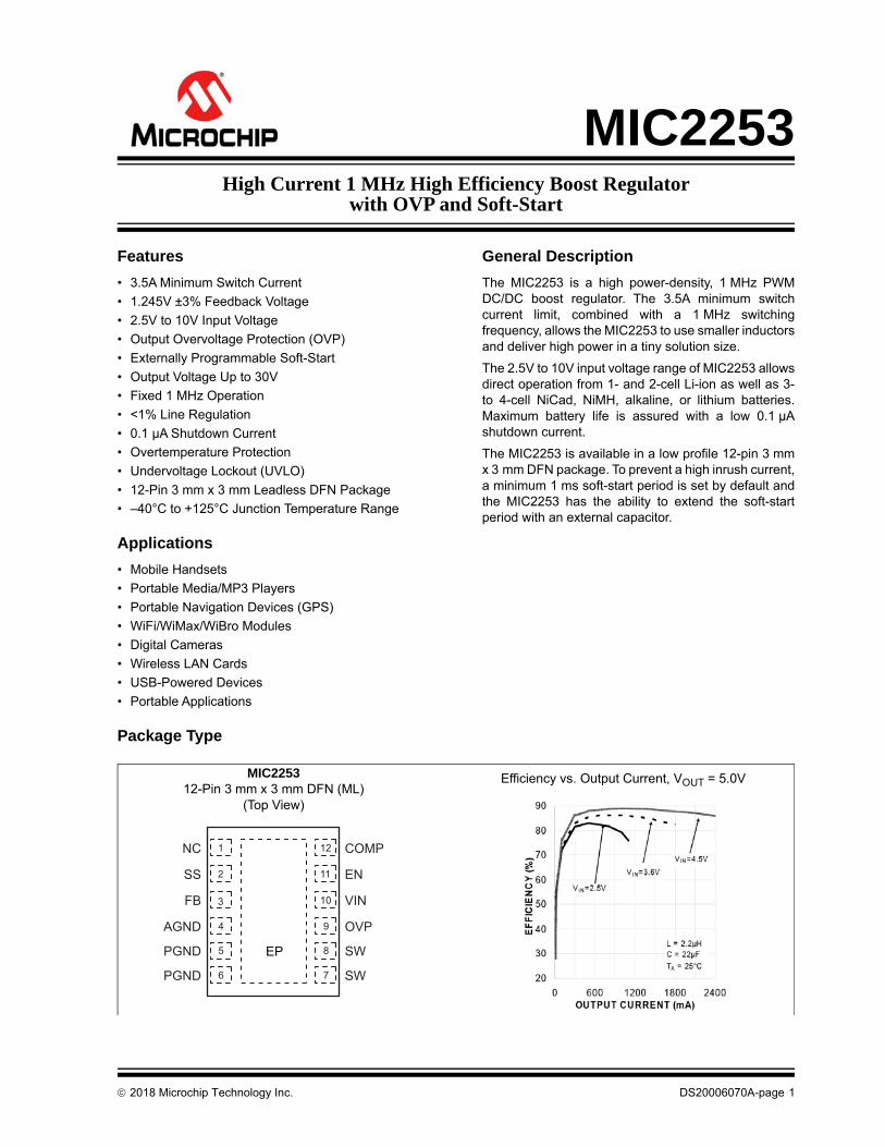
Package Type
PGND SW5
1NC
SS
FB
AGND
12 COMP
EN
VIN
OVP
11
10
9
2
3
4
8EP
PGND SW6 7
MIC225312-Pin 3 mm x 3 mm DFN (ML)
(Top View)
Efficiency vs. Output Current, VOUT = 5.0V
High Current 1 MHz High Efficiency Boost Regulatorwith OVP and Soft-Start
MIC2253
DS20006070A-page 2 2018 Microchip Technology Inc.
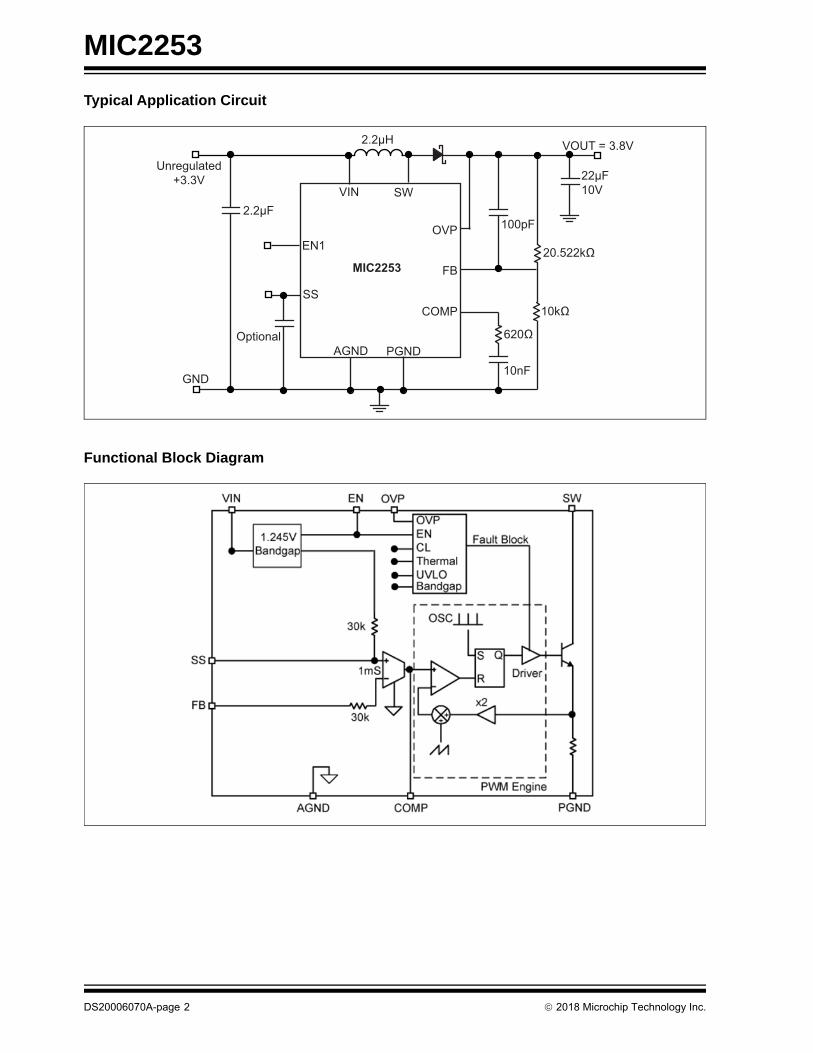
Typical Application Circuit
Functional Block Diagram
MIC2253
VIN SW
EN1OVP
SS
FB
COMP
PGNDAGND
2.2μH
Unregulated+3.3V
2.2μF
Optional
GND
100pF
10nF
22μF10V
VOUT = 3.8V
2018 Microchip Technology Inc. DS20006070A-page 3
MIC2253
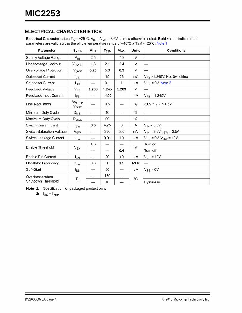
1.0 ELECTRICAL CHARACTERISTICS
Absolute Maximum Ratings †
Supply Voltage (VIN) .................................................................................................................................................+12VSwitch Voltage (VSW) ................................................................................................................................. –0.3V to +34VEnable Voltage (VEN) ................................................................................................................................... –0.3V to 12VFB Voltage (VFB) .........................................................................................................................................................+6VSwitch Current (ISW) .............................................................................................................................. Internally LimitedAmbient Storage Temperature (TS)........................................................................................................ –65°C to +150°CESD Rating (Note 1) .................................................................................................................................................. 2 kV
Operating Ratings ††
Supply Voltage (VIN) .................................................................................................................................. +2.5V to +10VEnable Voltage (VEN) ..........................................................................................................................................0V to VINJunction Temperature (TJ)...................................................................................................................... –40°C to +125°CPackage Thermal Resistance3 mm x 3 mm DFN-12 (JA) ..................................................................................................................................60°C/W
† Notice: Stresses above those listed under “Absolute Maximum Ratings” may cause permanent damage to the device.This is a stress rating only and functional operation of the device at those or any other conditions above those indicatedin the operational sections of this specification is not intended. Exposure to maximum rating conditions for extendedperiods may affect device reliability.
†† Notice: The device is not guaranteed to function outside its operating ratings.
Note 1: Devices are ESD sensitive. Handling precautions are recommended. Human body model, 1.5 kΩ in serieswith 100 pF.
MIC2253
DS20006070A-page 4 2018 Microchip Technology Inc.
ELECTRICAL CHARACTERISTICS
Electrical Characteristics: TA = +25°C; VIN = VEN = 3.6V; unless otherwise noted. Bold values indicate that parameters are valid across the whole temperature range of –40°C ≤ TJ ≤ +125°C. Note 1
Parameter Sym. Min. Typ. Max. Units Conditions
Supply Voltage Range VIN 2.5 — 10 V —
Undervoltage Lockout VUVLO 1.8 2.1 2.4 V —
Overvoltage Protection VOVP 5.25 5.6 6.3 V —
Quiescent Current IVIN — 15 23 mA VFB >1.245V, Not Switching
Shutdown Current ISD — 0.1 1 µA VEN = 0V, Note 2
Feedback Voltage VFB 1.208 1.245 1.283 V —
Feedback Input Current IFB — –450 — nA VFB = 1.245V
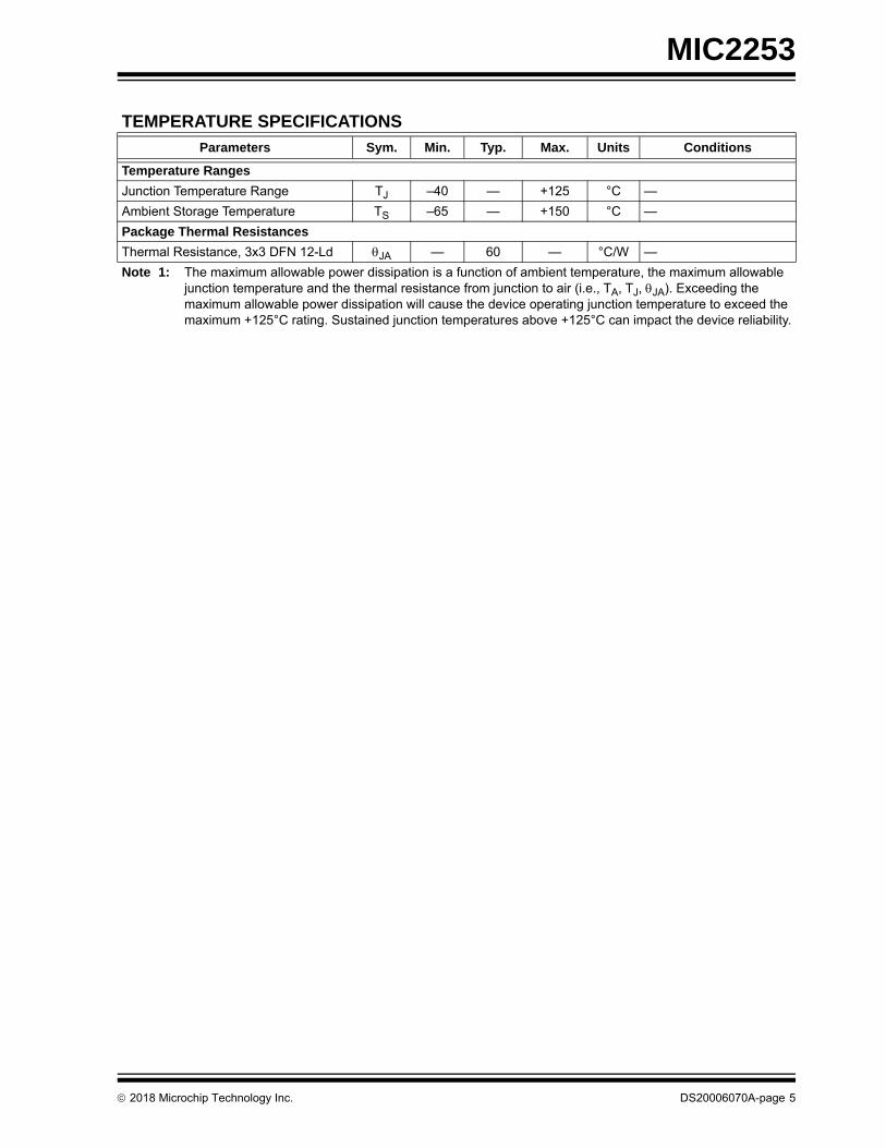
Note 1: The maximum allowable power dissipation is a function of ambient temperature, the maximum allowable junction temperature and the thermal resistance from junction to air (i.e., TA, TJ, JA). Exceeding the maximum allowable power dissipation will cause the device operating junction temperature to exceed the maximum +125°C rating. Sustained junction temperatures above +125°C can impact the device reliability.
MIC2253
DS20006070A-page 6 2018 Microchip Technology Inc.
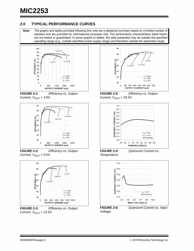
2.0 TYPICAL PERFORMANCE CURVES
FIGURE 2-1: Efficiency vs. Output Current, VOUT = 3.8V.
FIGURE 2-2: Efficiency vs. Output Current, VOUT = 5.0V.
FIGURE 2-3: Efficiency vs. Output Current, VOUT = 12.0V.
FIGURE 2-4: Efficiency vs. Output Current, VOUT = 15.0V.
FIGURE 2-5: Quiescent Current vs. Temperature.
FIGURE 2-6: Quiescent Current vs. Input Voltage.
Note: The graphs and tables provided following this note are a statistical summary based on a limited number ofsamples and are provided for informational purposes only. The performance characteristics listed hereinare not tested or guaranteed. In some graphs or tables, the data presented may be outside the specifiedoperating range (e.g., outside specified power supply range) and therefore outside the warranted range.
2018 Microchip Technology Inc. DS20006070A-page 7
MIC2253
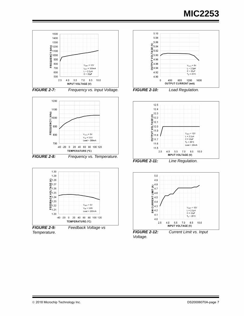
FIGURE 2-7: Frequency vs. Input Voltage.
FIGURE 2-8: Frequency vs. Temperature.
FIGURE 2-9: Feedback Voltage vs Temperature.
FIGURE 2-10: Load Regulation.
FIGURE 2-11: Line Regulation.
FIGURE 2-12: Current Limit vs. Input Voltage.
MIC2253
DS20006070A-page 8 2018 Microchip Technology Inc.
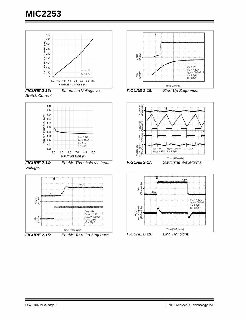
FIGURE 2-13: Saturation Voltage vs. Switch Current.
FIGURE 2-14: Enable Threshold vs. Input Voltage.
FIGURE 2-15: Enable Turn-On Sequence.
FIGURE 2-16: Start-Up Sequence.
FIGURE 2-17: Switching Waveforms.
FIGURE 2-18: Line Transient.
2018 Microchip Technology Inc. DS20006070A-page 9
MIC2253
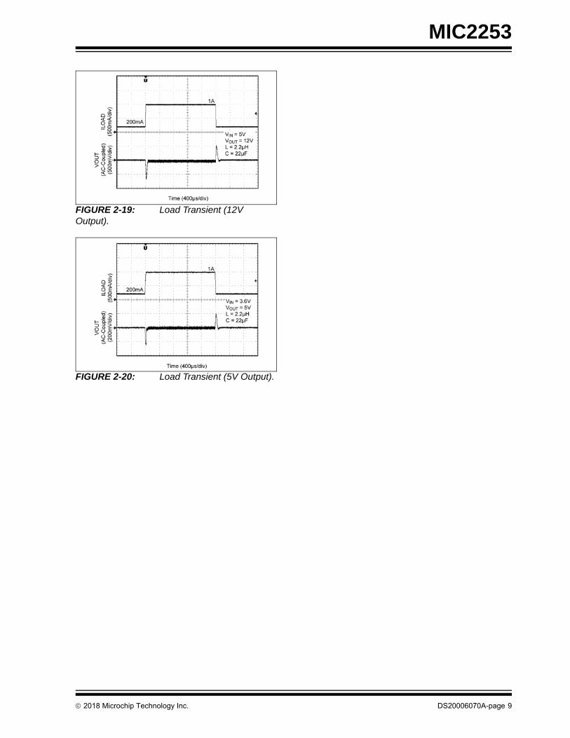
FIGURE 2-19: Load Transient (12V Output).
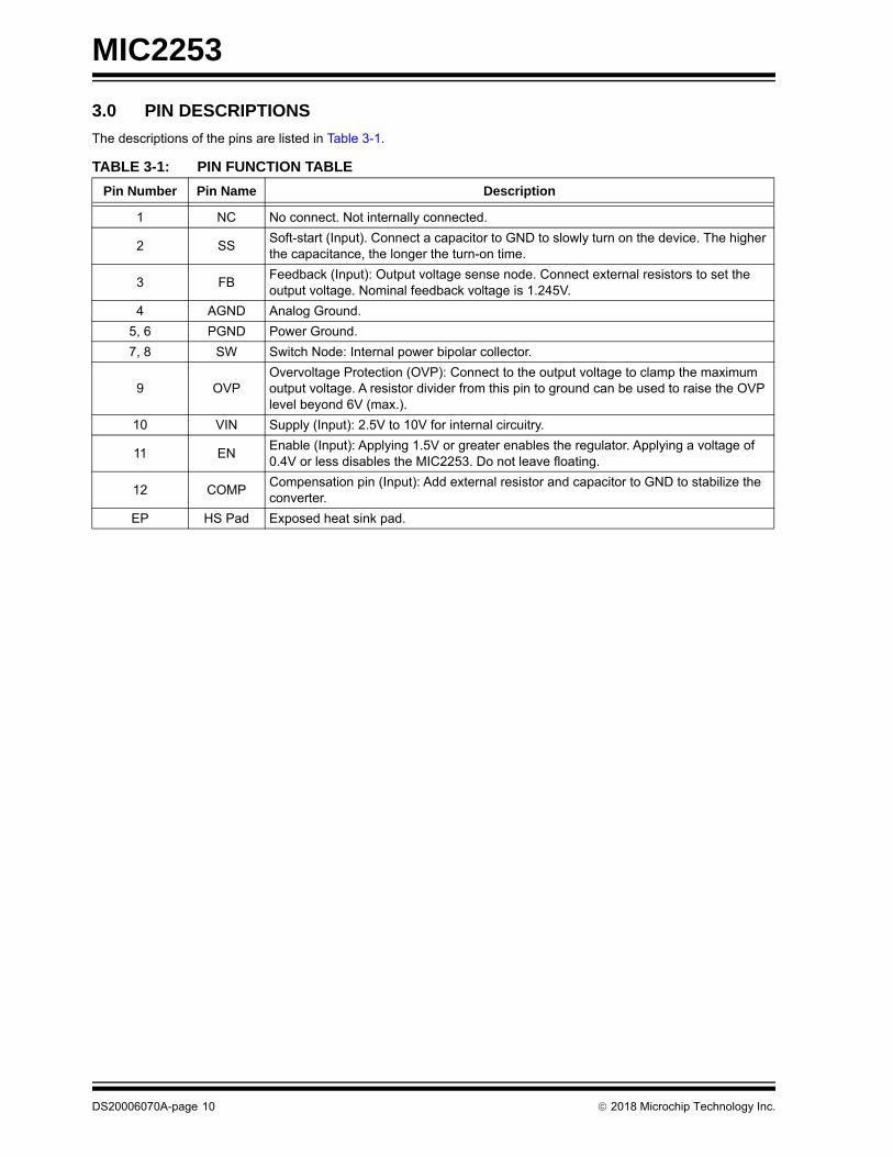
FIGURE 2-20: Load Transient (5V Output).
MIC2253
DS20006070A-page 10 2018 Microchip Technology Inc.
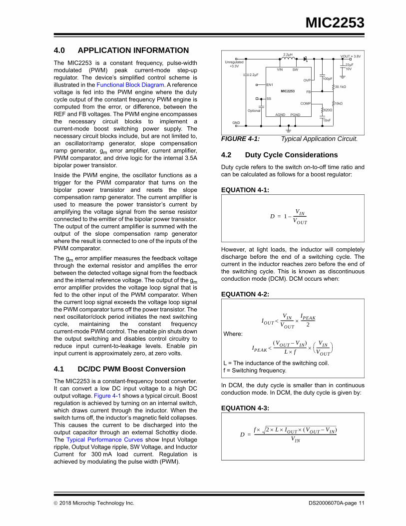
3.0 PIN DESCRIPTIONS
The descriptions of the pins are listed in Table 3-1.
TABLE 3-1: PIN FUNCTION TABLE
Pin Number Pin Name Description
1 NC No connect. Not internally connected.
2 SSSoft-start (Input). Connect a capacitor to GND to slowly turn on the device. The higher the capacitance, the longer the turn-on time.
3 FBFeedback (Input): Output voltage sense node. Connect external resistors to set the output voltage. Nominal feedback voltage is 1.245V.
4 AGND Analog Ground.
5, 6 PGND Power Ground.
7, 8 SW Switch Node: Internal power bipolar collector.
9 OVPOvervoltage Protection (OVP): Connect to the output voltage to clamp the maximum output voltage. A resistor divider from this pin to ground can be used to raise the OVP level beyond 6V (max.).
10 VIN Supply (Input): 2.5V to 10V for internal circuitry.
11 ENEnable (Input): Applying 1.5V or greater enables the regulator. Applying a voltage of 0.4V or less disables the MIC2253. Do not leave floating.
12 COMPCompensation pin (Input): Add external resistor and capacitor to GND to stabilize the converter.
EP HS Pad Exposed heat sink pad.
2018 Microchip Technology Inc. DS20006070A-page 11
MIC2253
4.0 APPLICATION INFORMATION
The MIC2253 is a constant frequency, pulse-widthmodulated (PWM) peak current-mode step-upregulator. The device’s simplified control scheme isillustrated in the Functional Block Diagram. A referencevoltage is fed into the PWM engine where the dutycycle output of the constant frequency PWM engine iscomputed from the error, or difference, between theREF and FB voltages. The PWM engine encompassesthe necessary circuit blocks to implement acurrent-mode boost switching power supply. Thenecessary circuit blocks include, but are not limited to,an oscillator/ramp generator, slope compensationramp generator, gm error amplifier, current amplifier,PWM comparator, and drive logic for the internal 3.5Abipolar power transistor.
Inside the PWM engine, the oscillator functions as atrigger for the PWM comparator that turns on thebipolar power transistor and resets the slopecompensation ramp generator. The current amplifier isused to measure the power transistor’s current byamplifying the voltage signal from the sense resistorconnected to the emitter of the bipolar power transistor.The output of the current amplifier is summed with theoutput of the slope compensation ramp generatorwhere the result is connected to one of the inputs of thePWM comparator.
The gm error amplifier measures the feedback voltagethrough the external resistor and amplifies the errorbetween the detected voltage signal from the feedbackand the internal reference voltage. The output of the gmerror amplifier provides the voltage loop signal that isfed to the other input of the PWM comparator. Whenthe current loop signal exceeds the voltage loop signalthe PWM comparator turns off the power transistor. Thenext oscillator/clock period initiates the next switchingcycle, maintaining the constant frequencycurrent-mode PWM control. The enable pin shuts downthe output switching and disables control circuitry toreduce input current-to-leakage levels. Enable pininput current is approximately zero, at zero volts.
4.1 DC/DC PWM Boost Conversion
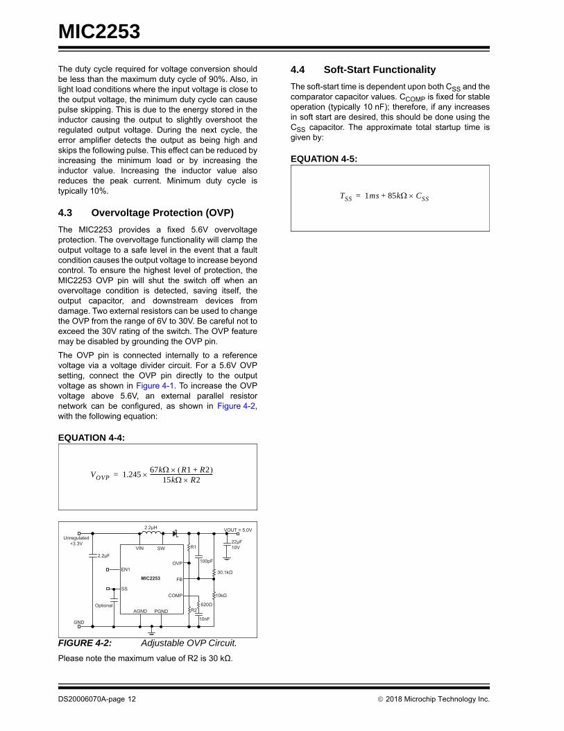
The MIC2253 is a constant-frequency boost converter.It can convert a low DC input voltage to a high DCoutput voltage. Figure 4-1 shows a typical circuit. Boostregulation is achieved by turning on an internal switch,which draws current through the inductor. When theswitch turns off, the inductor’s magnetic field collapses.This causes the current to be discharged into theoutput capacitor through an external Schottky diode.The Typical Performance Curves show Input Voltageripple, Output Voltage ripple, SW Voltage, and InductorCurrent for 300 mA load current. Regulation isachieved by modulating the pulse width (PWM).
FIGURE 4-1: Typical Application Circuit.
4.2 Duty Cycle Considerations
Duty cycle refers to the switch on-to-off time ratio andcan be calculated as follows for a boost regulator:
EQUATION 4-1:
However, at light loads, the inductor will completelydischarge before the end of a switching cycle. Thecurrent in the inductor reaches zero before the end ofthe switching cycle. This is known as discontinuousconduction mode (DCM). DCM occurs when:
EQUATION 4-2:
In DCM, the duty cycle is smaller than in continuousconduction mode. In DCM, the duty cycle is given by:
EQUATION 4-3:
MIC2253
VIN SW
EN1OVP
SS
FB
COMP
PGNDAGND
2.2μH
Unregulated+3.3V
2.2μF
Optional
GND
100pF
10nF
22μF10V
VOUT = 3.8V
D 1VIN
VOUT-------------–=
IOUT
VIN
VOUT-------------
IPEAK
2--------------
Where:
L = The inductance of the switching coil.f = Switching frequency.
DS20006070A-page 12 2018 Microchip Technology Inc.
The duty cycle required for voltage conversion shouldbe less than the maximum duty cycle of 90%. Also, inlight load conditions where the input voltage is close tothe output voltage, the minimum duty cycle can causepulse skipping. This is due to the energy stored in theinductor causing the output to slightly overshoot theregulated output voltage. During the next cycle, theerror amplifier detects the output as being high andskips the following pulse. This effect can be reduced byincreasing the minimum load or by increasing theinductor value. Increasing the inductor value alsoreduces the peak current. Minimum duty cycle istypically 10%.
4.3 Overvoltage Protection (OVP)
The MIC2253 provides a fixed 5.6V overvoltageprotection. The overvoltage functionality will clamp theoutput voltage to a safe level in the event that a faultcondition causes the output voltage to increase beyondcontrol. To ensure the highest level of protection, theMIC2253 OVP pin will shut the switch off when anovervoltage condition is detected, saving itself, theoutput capacitor, and downstream devices fromdamage. Two external resistors can be used to changethe OVP from the range of 6V to 30V. Be careful not toexceed the 30V rating of the switch. The OVP featuremay be disabled by grounding the OVP pin.
The OVP pin is connected internally to a referencevoltage via a voltage divider circuit. For a 5.6V OVPsetting, connect the OVP pin directly to the outputvoltage as shown in Figure 4-1. To increase the OVPvoltage above 5.6V, an external parallel resistornetwork can be configured, as shown in Figure 4-2,with the following equation:
EQUATION 4-4:
FIGURE 4-2: Adjustable OVP Circuit.
Please note the maximum value of R2 is 30 kΩ.
4.4 Soft-Start Functionality
The soft-start time is dependent upon both CSS and thecomparator capacitor values. CCOMP is fixed for stableoperation (typically 10 nF); therefore, if any increasesin soft start are desired, this should be done using theCSS capacitor. The approximate total startup time isgiven by:
2018 Microchip Technology Inc. DS20006070A-page 13
MIC2253
5.0 COMPONENT SELECTION
5.1 Inductor
The MIC2253 is designed to work with a 2.2 µHinductor. This is due to the unavoidable “right half planezero” effect for the continuous current boost convertertopology. The frequency at which the right half planezero occurs can be calculated as follows:
EQUATION 5-1:
The right half plane zero has the undesirable effect ofincreasing gain, while decreasing phase. This requiresthat the loop gain is rolled off before this has significanteffect on the total loop response. This can beaccomplished by either reducing inductance(increasing RHPZ frequency) or increasing the outputcapacitor value (decreasing loop gain).
5.2 Output Capacitor
Output capacitor selection is a trade-off betweenperformance, size, and cost. Increasing outputcapacitance will lead to an improved transientresponse, but also an increase in size and cost. X5R orX7R dielectric ceramic capacitors are recommendedfor designs with the MIC2253.
The output capacitor sets the frequency of thedominant pole and zero in the power stage. The zero isgiven by:
EQUATION 5-2:
For ceramic capacitors, the ESR is very small. Thisputs the zero at a very high frequency where it can beignored. Fortunately, the MIC2253 is current mode inoperation which reduces the need for this outputcapacitor zero when compensating the feedback loop.
The frequency of the pole caused by the outputcapacitor is given by:
EQUATION 5-3:
5.3 Diode Selection
The MIC2253 requires an external diode for operation.A Schottky diode is recommended for mostapplications due to their lower forward voltage drop andreverse recovery time. Make sure that the diodeselected can deliver the peak inductor current and themaximum reverse voltage is rated greater than theoutput voltage.
5.4 Input Capacitor
A minimum 2.2 µF ceramic capacitor with an X5R orX7R dielectric is recommended for designing with theMIC2253. Increasing input capacitance will improveperformance and greater noise immunity on thesource. The input capacitor should be as close aspossible to the inductor and the MIC2253, with shorttraces for good noise performance.
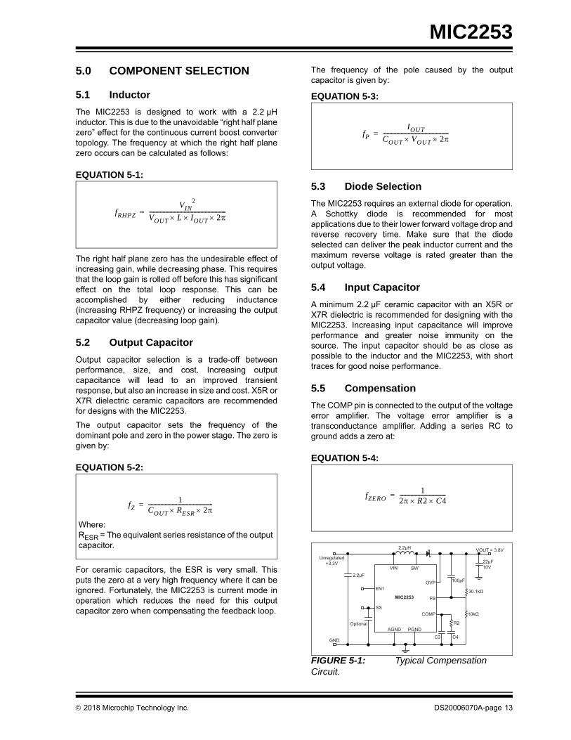
5.5 Compensation
The COMP pin is connected to the output of the voltageerror amplifier. The voltage error amplifier is atransconductance amplifier. Adding a series RC toground adds a zero at:
EQUATION 5-4:
FIGURE 5-1: Typical Compensation Circuit.
fRHPZ
VIN2
VOUT L IOUT 2-------------------------------------------------------=
DS20006070A-page 14 2018 Microchip Technology Inc.
The resistor should be set to approximately 600Ω. Thecapacitor typically ranges from 10 nF to 100 nF.
Adding an optional capacitor from the COMP pin toground adds a pole at approximately:
EQUATION 5-5:
This capacitor typically is 100 pF. Generally, an RC toground is all that is needed. The RC should be placedas close as possible to the COMP pin. The capacitorshould be a ceramic with a X5R, X7R, or COGdielectric. Refer to the MIC2253 evaluation boarduser’s guide document for component location.
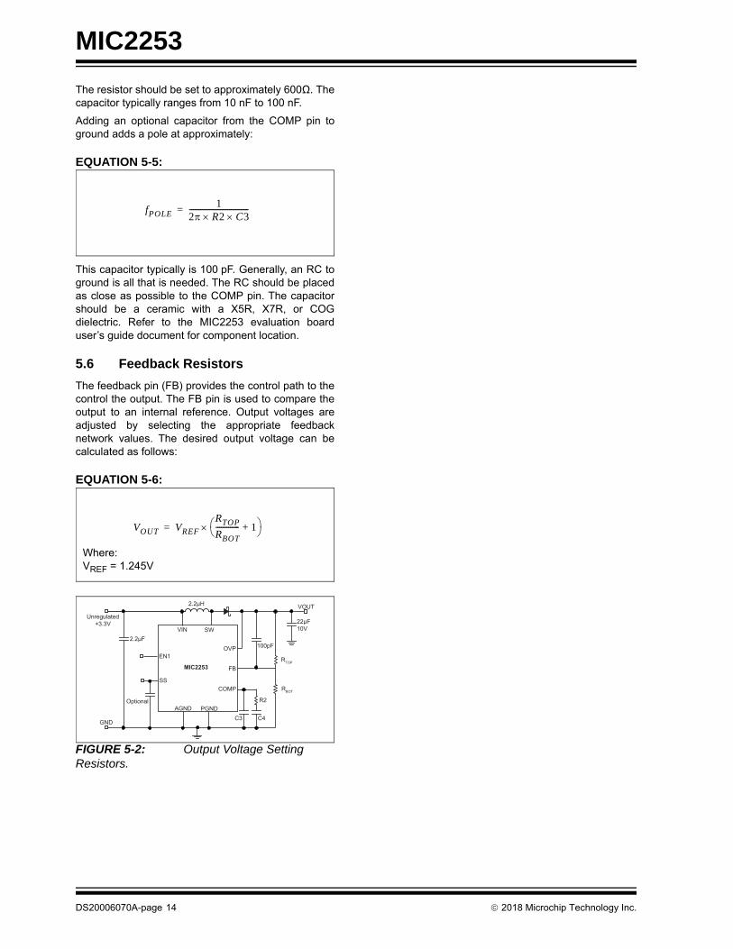
5.6 Feedback Resistors
The feedback pin (FB) provides the control path to thecontrol the output. The FB pin is used to compare theoutput to an internal reference. Output voltages areadjusted by selecting the appropriate feedbacknetwork values. The desired output voltage can becalculated as follows:
EQUATION 5-6:
FIGURE 5-2: Output Voltage Setting Resistors.
fPOLE1
2 R2 C3---------------------------------=
VOUT VREF
RTOP
RBOT------------- 1+ =
Where:VREF = 1.245V
MIC2253
VIN SW
EN1OVP
SS
FB
COMP
PGNDAGND
2.2μH
Unregulated+3.3V
2.2μF
Optional
GND
100pF
R2
RBOT
C4
RTOP
22μF10V
VOUT
C3
2018 Microchip Technology Inc. DS20006070A-page 15
MIC2253
6.0 PACKAGING INFORMATION
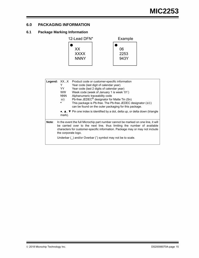
6.1 Package Marking Information
12-Lead DFN* Example
XXXXXXNNNY
062253943Y
Legend: XX...X Product code or customer-specific informationY Year code (last digit of calendar year)YY Year code (last 2 digits of calendar year)WW Week code (week of January 1 is week ‘01’)NNN Alphanumeric traceability code Pb-free JEDEC® designator for Matte Tin (Sn)* This package is Pb-free. The Pb-free JEDEC designator ( )
can be found on the outer packaging for this package.
, , Pin one index is identified by a dot, delta up, or delta down (trianglemark).
Note: In the event the full Microchip part number cannot be marked on one line, it willbe carried over to the next line, thus limiting the number of availablecharacters for customer-specific information. Package may or may not includethe corporate logo.
Underbar (_) and/or Overbar (⎯) symbol may not be to scale.
3e
3e
MIC2253
DS20006070A-page 16 2018 Microchip Technology Inc.
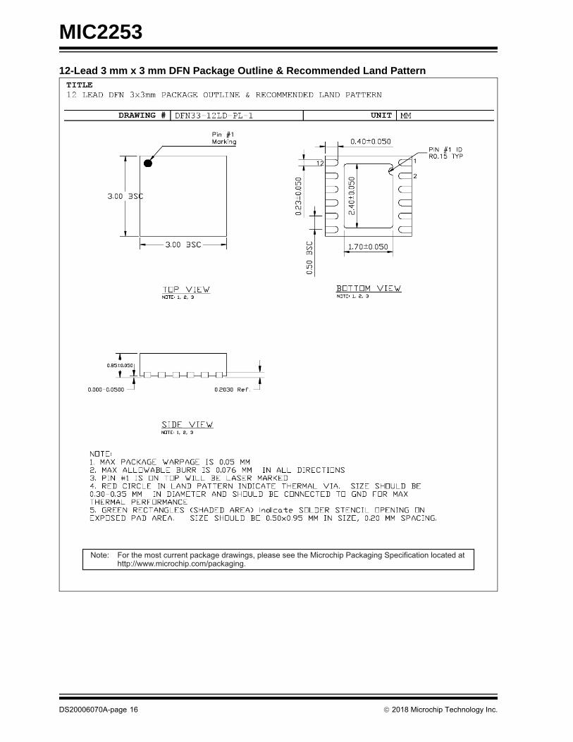
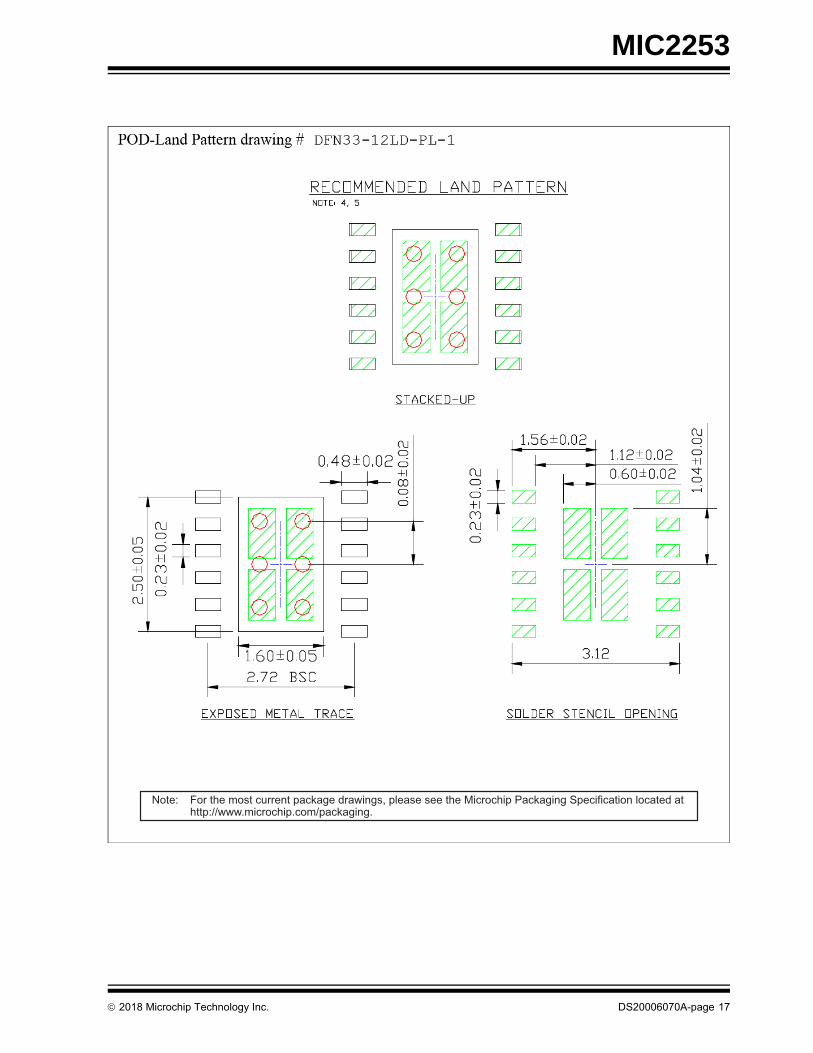
12-Lead 3 mm x 3 mm DFN Package Outline & Recommended Land Pattern
Note: For the most current package drawings, please see the Microchip Packaging Specification located at http://www.microchip.com/packaging.
2018 Microchip Technology Inc. DS20006070A-page 17
MIC2253
Note: For the most current package drawings, please see the Microchip Packaging Specification located at http://www.microchip.com/packaging.
MIC2253
DS20006070A-page 18 2018 Microchip Technology Inc.
NOTES:
2018 Microchip Technology Inc. DS20006070A-page 19
MIC2253
APPENDIX A: REVISION HISTORY
Revision A (September 2018)
• Converted Micrel document MIC2253 to Micro-chip data sheet template DS2000xxxxA.
• Minor grammatical text changes throughout.
• Added Figure 5-1 and Figure 5-2.
MIC2253
DS20006070A-page 20 2018 Microchip Technology Inc.
NOTES:
2018 Microchip Technology Inc. DS20006070A-page 21
MIC2253
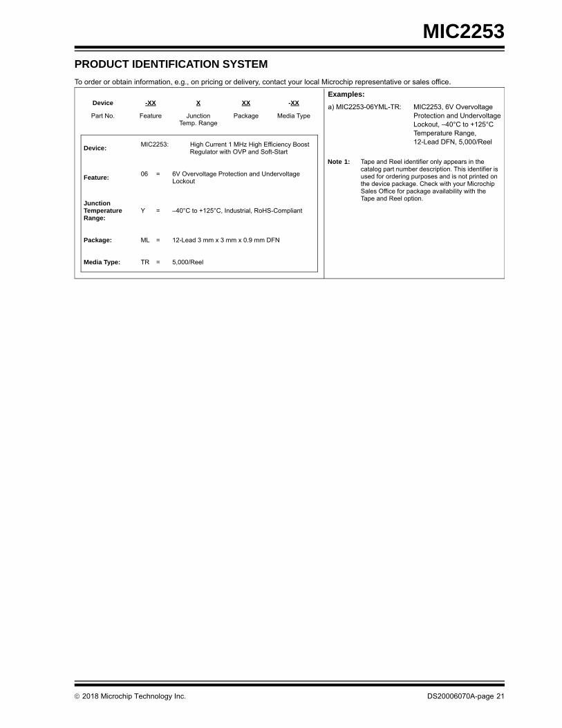
PRODUCT IDENTIFICATION SYSTEM
To order or obtain information, e.g., on pricing or delivery, contact your local Microchip representative or sales office.
Examples:
a) MIC2253-06YML-TR: MIC2253, 6V Overvoltage Protection and Undervoltage Lockout, –40°C to +125°C Temperature Range, 12-Lead DFN, 5,000/Reel
Device:MIC2253: High Current 1 MHz High Efficiency Boost
Regulator with OVP and Soft-Start
Feature:06 = 6V Overvoltage Protection and Undervoltage
Lockout
Junction Temperature Range:
Y = –40°C to +125°C, Industrial, RoHS-Compliant
Package: ML = 12-Lead 3 mm x 3 mm x 0.9 mm DFN
Media Type: TR = 5,000/Reel
Note 1: Tape and Reel identifier only appears in the catalog part number description. This identifier is used for ordering purposes and is not printed on the device package. Check with your Microchip Sales Office for package availability with the Tape and Reel option.
Device -XX X XX -XX
Part No. Feature Junction Temp. Range
Package Media Type
MIC2253
DS20006070A-page 22 2018 Microchip Technology Inc.
NOTES:
2018 Microchip Technology Inc. DS20006070A-page 23
Information contained in this publication regarding deviceapplications and the like is provided only for your convenienceand may be superseded by updates. It is your responsibility toensure that your application meets with your specifications.MICROCHIP MAKES NO REPRESENTATIONS ORWARRANTIES OF ANY KIND WHETHER EXPRESS ORIMPLIED, WRITTEN OR ORAL, STATUTORY OROTHERWISE, RELATED TO THE INFORMATION,INCLUDING BUT NOT LIMITED TO ITS CONDITION,QUALITY, PERFORMANCE, MERCHANTABILITY ORFITNESS FOR PURPOSE. Microchip disclaims all liabilityarising from this information and its use. Use of Microchipdevices in life support and/or safety applications is entirely atthe buyer’s risk, and the buyer agrees to defend, indemnify andhold harmless Microchip from any and all damages, claims,suits, or expenses resulting from such use. No licenses areconveyed, implicitly or otherwise, under any Microchipintellectual property rights unless otherwise stated.
Trademarks
The Microchip name and logo, the Microchip logo, AnyRate, AVR, AVR logo, AVR Freaks, BitCloud, chipKIT, chipKIT logo, CryptoMemory, CryptoRF, dsPIC, FlashFlex, flexPWR, Heldo, JukeBlox, KeeLoq, Kleer, LANCheck, LINK MD, maXStylus, maXTouch, MediaLB, megaAVR, MOST, MOST logo, MPLAB, OptoLyzer, PIC, picoPower, PICSTART, PIC32 logo, Prochip Designer, QTouch, SAM-BA, SpyNIC, SST, SST Logo, SuperFlash, tinyAVR, UNI/O, and XMEGA are registered trademarks of Microchip Technology Incorporated in the U.S.A. and other countries.
ClockWorks, The Embedded Control Solutions Company, EtherSynch, Hyper Speed Control, HyperLight Load, IntelliMOS, mTouch, Precision Edge, and Quiet-Wire are registered trademarks of Microchip Technology Incorporated in the U.S.A.
Adjacent Key Suppression, AKS, Analog-for-the-Digital Age, Any Capacitor, AnyIn, AnyOut, BodyCom, CodeGuard, CryptoAuthentication, CryptoAutomotive, CryptoCompanion, CryptoController, dsPICDEM, dsPICDEM.net, Dynamic Average Matching, DAM, ECAN, EtherGREEN, In-Circuit Serial Programming, ICSP, INICnet, Inter-Chip Connectivity, JitterBlocker, KleerNet, KleerNet logo, memBrain, Mindi, MiWi, motorBench, MPASM, MPF, MPLAB Certified logo, MPLIB, MPLINK, MultiTRAK, NetDetach, Omniscient Code Generation, PICDEM, PICDEM.net, PICkit, PICtail, PowerSmart, PureSilicon, QMatrix, REAL ICE, Ripple Blocker, SAM-ICE, Serial Quad I/O, SMART-I.S., SQI, SuperSwitcher, SuperSwitcher II, Total Endurance, TSHARC, USBCheck, VariSense, ViewSpan, WiperLock, Wireless DNA, and ZENA are trademarks of Microchip Technology Incorporated in the U.S.A. and other countries.
SQTP is a service mark of Microchip Technology Incorporated in the U.S.A.
Silicon Storage Technology is a registered trademark of Microchip Technology Inc. in other countries.
GestIC is a registered trademark of Microchip Technology Germany II GmbH & Co. KG, a subsidiary of Microchip Technology Inc., in other countries.
All other trademarks mentioned herein are property of their respective companies.
Note the following details of the code protection feature on Microchip devices:
• Microchip products meet the specification contained in their particular Microchip Data Sheet.
• Microchip believes that its family of products is one of the most secure families of its kind on the market today, when used in the intended manner and under normal conditions.
• There are dishonest and possibly illegal methods used to breach the code protection feature. All of these methods, to our knowledge, require using the Microchip products in a manner outside the operating specifications contained in Microchip’s Data Sheets. Most likely, the person doing so is engaged in theft of intellectual property.
• Microchip is willing to work with the customer who is concerned about the integrity of their code.
• Neither Microchip nor any other semiconductor manufacturer can guarantee the security of their code. Code protection does not mean that we are guaranteeing the product as “unbreakable.”
Code protection is constantly evolving. We at Microchip are committed to continuously improving the code protection features of ourproducts. Attempts to break Microchip’s code protection feature may be a violation of the Digital Millennium Copyright Act. If such actsallow unauthorized access to your software or other copyrighted work, you may have a right to sue for relief under that Act.
Microchip received ISO/TS-16949:2009 certification for its worldwide headquarters, design and wafer fabrication facilities in Chandler and Tempe, Arizona; Gresham, Oregon and design centers in California and India. The Company’s quality system processes and procedures are for its PIC® MCUs and dsPIC® DSCs, KEELOQ® code hopping devices, Serial EEPROMs, microperipherals, nonvolatile memory and analog products. In addition, Microchip’s quality system for the design and manufacture of development systems is ISO 9001:2000 certified.
QUALITYMANAGEMENTSYSTEMCERTIFIEDBYDNV
== ISO/TS16949==
DS20006070A-page 24 2018 Microchip Technology Inc.
AMERICASCorporate Office2355 West Chandler Blvd.Chandler, AZ 85224-6199Tel: 480-792-7200 Fax: 480-792-7277Technical Support: http://www.microchip.com/supportWeb Address: www.microchip.com
AtlantaDuluth, GA Tel: 678-957-9614 Fax: 678-957-1455
Austin, TXTel: 512-257-3370
BostonWestborough, MA Tel: 774-760-0087 Fax: 774-760-0088
ChicagoItasca, IL Tel: 630-285-0071 Fax: 630-285-0075


![OVP-M3 - Shanghai ONBON Technology Inc. USER MANUAL.pdf · OVP-M3havethreeareas:INPUT、FUNCION、MENU. INPUT area Therearesixbuttonsinthisarea:[DVI]button、[HDMI]button、[CV1]button、](https://static.documents.pub/doc/80x56/5e367ff6d5815309280bc393/ovp-m3-shanghai-onbon-technology-inc-user-manualpdf-ovp-m3havethreeareasiinputfuncionmenu.jpg)


