National Aeronautics and Space Administration High-Density 3D TSOP Stack Packaging NEPP FY11 Summary Report Phillip Zulueta Jet Propulsion Laboratory Pasadena, California Jet Propulsion Laboratory California Institute of Technology Pasadena, California JPL Publication 12-2 2/12
Transcript
National Aeronautics and Space Administration
High-Density 3D TSOP Stack Packaging NEPP FY11 Summary Report
Phillip Zulueta
Jet Propulsion Laboratory Pasadena, California
Jet Propulsion Laboratory California Institute of Technology
Pasadena, California
JPL Publication 12-2 2/12
i
National Aeronautics and Space Administration
High-Density 3D TSOP Stack Packaging NEPP FY11 Summary Report
NASA Electronic Parts and Packaging (NEPP) Program
Office of Safety and Mission Assurance
Phillip Zulueta Jet Propulsion Laboratory
Pasadena, California
NASA WBS: 724297.40.49.11 JPL Project Number: 104593 Task Number: 40.49.02.05
Jet Propulsion Laboratory 4800 Oak Grove Drive Pasadena, CA 91109
http://nepp.nasa.gov
ii
This research was carried out at the Jet Propulsion Laboratory (JPL), California Institute of Technology, and was
sponsored by the National Aeronautics and Space Administration Electronic Parts and Packaging (NEPP) Program.
Reference herein to any specific commercial product, process, or service by trade name, trademark, manufacturer, or
otherwise, does not constitute or imply its endorsement by the United States Government or the Jet Propulsion
Laboratory, California Institute of Technology.
Copyright 2012. California Institute of Technology. Government sponsorship acknowledged.
ACKNOWLEDGMENTS
The author acknowledges individuals from both Interconnect Systems, Inc. (ISI) and JPL who were critical in the
progress of this activity; specifically, Dr. Robert D. Gerke, who initiated this task and Dr. Reza Ghaffarian, who
facilitated the testing. The author extends appreciation to program managers of the NEPP Program—Michael
Sampson, Ken Label, and Dr. Charles Barnes—for their continuous support and encouragement.
iii
TABLE OF CONTENTS 1.0 Introduction ........................................................................................................................................................... 1
2.0 High-Density 3D Packaging Trends ...................................................................................................................... 2 2.1 Stacked Wire-Bonded Die ............................................................................................................................ 2 2.2 Package-on-Package (PoP) ......................................................................................................................... 3 2.3 Package-in-Package (PiP) ........................................................................................................................... 3 2.4 Through Silicon Via (TSV) ............................................................................................................................ 3
6.0 Summary and Recommendations ....................................................................................................................... 11
1
1.0 INTRODUCTION This report documents a reliability evaluation of a particular implementation of package-on-package (PoP) high-density electronic packaging technology. Package-on-package is just one of several new high density packaging technologies that offer significant reductions in overall required PCB board area while allowing for significant and often unique increases in device performance and functionality. The particular PoP technology tested for this report was provided by Interconnect Systems, Inc. (ISI). ISI utilizes standard, readily available device packaging methods in which high-density packaging is achieved through a combination of several technologies:
• Standard packaged memory devices • 3-dimensional (3D) interconnect assembly
In general, 3D packaging provides a high level of functional integration in well-established package families (i.e., ball grid arrays [BGAs] and lead-frame packages) by using stacking die, stacking packages, or a mix of both, and a combination of assembly technologies including wire bonding, flip-chip, and surface mount solder operations. These technologies offer cost-effective solutions for low or medium volume applications, typically used in NASA projects. This task examined a particular type of high-density packaging used for flash memory in thin, small outline packages (TSOPs) in a soldered, stacked configuration. The stackable package contains pads on the top of the package that facilitate the stacking process.
This task is a result of a recommendation from the 2007 NEPP Packaging Roadmap.
2
2.0 HIGH-DENSITY 3D PACKAGING TRENDS Flash memory has become a fundamental building block in today’s electronic systems and is an ideal candidate for integrated memory implementation. Its content can be changed in the field and thus provides broad flexibility in applications. The increasing use of flash memory in today’s electronic systems is helping drive the trend in high-density electronics packaging to the extent that packaging has migrated to the third dimension (3D) and has now become mainstream technology. These new packaging configurations can combine flip chips, wire-bond interconnection, solder, laminate substrates, and over-molding of module assemblies. Package-level integration of disparate device functions is possible and produced through 3D die and package stacking. However, wire-bonding remains the most popular method for low-density connections of less than 200 input/output (I/O) per chip; although it is becoming more difficult to meet the demands for wiring connectivity merely by increasing the number of the peripheral wire-bonds. In order to overcome such wiring connectivity issues, 3D chip stacking technology using through-silicon-via (TSV) technology is attractive because it offers the possibility of solving the serious interconnection problems while offering integrated functions for higher performance. TSV is a novel packaging technology that JPL continues to monitor for future NASA applications.
2.1 Stacked Wire-Bonded Die Vertical chip stacking is performed as chip-to-chip, chip-to-wafer, or wafer-to-wafer processes. Stacked die packages consist of bare die stacked and interconnected using wire-bond and flip-chip connections in one standard package. Figure 2.1-1 shows an example of this. This packaging technology results in the thinnest package with the lowest assembly cost and the potential for the highest board-level reliability. This is due to the fact that soldered interconnects are minimized. Low-profile wire bonding is a critical process for this technology. Stacked die utilizing silicon spacers or epoxy filled with spherical spacers are used to control die-to-die spacing. From a reliability standpoint, the addition of silicon into the package increases the bending resistance and the risk and/or vulnerability for cracks during assembly or qualification testing. These cracks can occur, either in the package body (molding compound) or in the die itself.
Figure 2.1-1. Stacked wire-bonded die.
Source: STATS ChipPAC
3
2.2 Package-on-Package (PoP) Package-on-package (PoP) is a package technology where pre-packaged devices are vertically stacked on top of each other using a lead-frame, printed wiring board, or flex interconnects to integrate different functionalities while still remaining a compact size. For example, combining memory and logic into a single PoP offers advantages in procurement, lower cost, better total system costs, and faster time to produce and integrate into applications. Electrically, PoP offers benefits by minimizing trace lengths between different interoperating parts, yielding better performance, faster signal propagation, and reduced noise and cross-talk. Another benefit is that separate testing (and burn-in) of each package can be conducted before assembly into the integrated structure.
PoP technology has advanced to the point where the JEDEC JC11 committee has developed guidelines and standards related to PoP technology. In March 2007, they released JEDEC Publication 95, Design Guide 4.21A, “Internal Stacking Module, Land Grid Array Packages with External Interconnect Terminals (ISM)” and in January 2009, they released MO-266C, a registration drawing for “Very Thin, Fine-Pitch, Stackable Ball Grid, 0.50 mm Ball Pitch Array Family, VF-XBGA.” Most recently, they released another registration standard in April 2010, MO-302A for “Very Thin, Fine-Pitch, Fully Overmolded, Stackable, Ball Grid Array Family, 0.40 mm Ball Pitch, VF-XBGA.”
PoP technology is not without manufacturing or reliability issues. As the stacked packages may be procured from different suppliers, there is a chance that their expansion coefficients can vary and cause warpage during and after the reflow joining process. Warpage is the result of residual stress induced by non-uniform package shrinkage. Various methods have been implemented to counter these effects. The addition of smaller solder balls on the top pad of the bottom package helps absorb the effect of package warpage, while keeping the total volume of solder paste used to a minimum. In addition, overmolding the assembly can help reduce the effect of these residual stresses.
2.3 Package-in-Package (PiP) Package-in-package (PiP) technology extends traditional packaging by utilizing a combination or “hybridization” of dissimilar packaging technologies. An example of this technology may contain individual die in flip-chip formats integrated with pre-packaged, pre-tested formats like PoP. Combining wire-bonded die on organic substrates or flex interconnected die may further miniaturize the package. Most challenges are in the construction of the package and include bumping of thin wafers, die cracking, thin die flip-chip attachment, underfilling, substrate and package warpage and parametric shifts in the die. Package integration requires innovative assembly techniques and more rigorous methodologies and assembly design rules for managing chip-package interactions.
2.4 Through Silicon Via (TSV) Stacked memory die is an ideal choice for using TSV technology as all interconnections of each die align with the corresponding die located above and below. Vertical electrical connections (vias) pass through the silicon wafer or die. This is a high-performance 3D packaging technique compared to PoP technology because via density can be substantially higher and trace lengths are shorter. Most device manufacturers are involved with TSV or variations of TSV technology. Glass interposer technology used in conjunction or in place of TSV technology is also being developed and noted in recent literature.
4
3.0 EVALUATION APPROACH
3.1 Package Construction The package selected for this evaluation utilizes PoP technology consisting of 48-lead TSOPs solder stacked (both 2-high and 4-high) and integrated into single dual-flat no-lead (DFN) packages (Figure 3.1-1) Topline dummy packages were used in a daisy chain configuration for interconnect testing (Figure 3.1-2). Lead-free solder was used in the stacking assembly process and 63Sn-37Pb solder was used to mount the package to the test board. Ablestik ABLEFILL® UF8828 MRCE underfill was applied after mounting to the board. This particular underfill exhibits high Tg and high-fracture toughness and is engineered to withstand the 260°C peak reflow temperature associated with Pb-free soldering. All material selections and assembly were performed by ISI. An example of the completed assembly is shown in Figure 3.1-3.
Figure 3.1-3. ISI 4-high TSOP stacked package surface-mounted and epoxy-underfilled.
3.2 Testing Thermal cycle testing was conducted in accordance with MIL-STD-883, Method 1010, Test Condition B (temperature cycling, −55°C to +125°C). See Figure 3.2-1 for typical profile. Series resistance was monitored periodically to 500 cycles and recorded.
6
Figure 3.2-1. Temperature cycle profile.
7
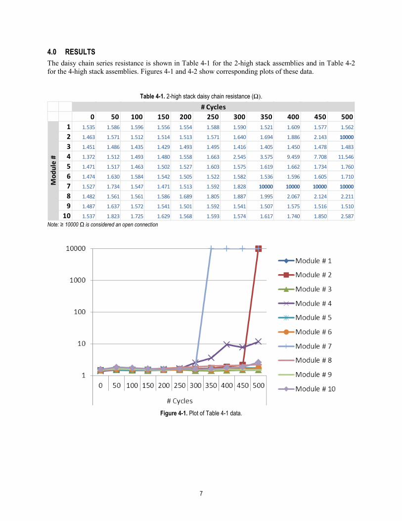
4.0 RESULTS The daisy chain series resistance is shown in Table 4-1 for the 2-high stack assemblies and in Table 4-2 for the 4-high stack assemblies. Figures 4-1 and 4-2 show corresponding plots of these data.
5.0 DISCUSSION The change in electrical resistance with the increasing number of temperature cycles is an indication of an imminent interconnection failure. An electrical resistance of greater than or equal to 10,000 ohms (Ω) is considered an electrical open, a clear failure. The 2-high stack package exhibited stability (arbitrarily less than 10% changes in resistance) within 250 cycles of testing, whereas the 4-high stack package became unstable (greater than 10% change in resistance) within 50–100 cycles of testing. Figure 5-1 is a plot of the cumulative percentage failures versus the number of temperature cycles. This figure shows that the 4-high stack has an increased failure rate over the 2-high stack by a factor of 1.43, which is the ratio of the slopes of the two linear fits for the data.
This significant increase in failure rate coupled with the steadily increasing resistance prior to failure means that the 4-high stack PoP approach implemented in this test is not acceptable for NASA applications.
Due to the limited amount of resources available for this task, a complete root cause failure analysis was not performed on any of the failures from the two different package assemblies. A general discussion of the possible failure mechanisms is provided for completeness, however. The location of these interconnection failures is either within the stack package itself, at the package-to-board interface, or at a combination of these two possible locations. Understanding the material aspects of the packaging construction is essential to not only the assembly of such parts, but also to the design of a reliable product. In this particular PoP construction, the package assembler has no control of the geometries or material selection used in the stacked configuration. It is entirely conceivable that the particular multiple materials of construction with varying coefficients of expansion (CTE), elastic moduli, and strengths contributed to the relatively low interconnection life exhibited in these results. In this particular PoP technology, the package assembler can only control the choice of solder and the associated processing, and whether to overmold the assembly (in which case, the assembler has a choice of overmold material). Overmolding can have some major effects on the CTE; however, in this case, no overmolding was conducted on the
Figure 5-1. Cumulative percentage failure vs. number of temperature cycles.
10
assemblies. From a board reliability standpoint, the user of these packaged assemblies has some control over the choice of board material, solder, and underfill. ISI had control over all material choices, except the TSOP packages and their geometries. The packages used in this evaluation were procured fully assembled, mounted, and underfilled to the test boards.
Isolation of the interconnection failures was not conducted due to the limited resources in this task. However, computed tomography x-ray was conducted on the parts with open interconnections in an attempt to visually isolate the failure. Figures 5-2 and 5-3 show composite images for the 2-high and 4-high stack assemblies, respectively.
Figure 5-2. Computed tomograph X-ray of the 2-high stack assembly.
Figure 5-3. Computed tomograph X-ray of the 4-high stack assembly.
11
6.0 SUMMARY AND RECOMMENDATIONS Although this particular PoP technology offers advantages in 3D high-density packaging with readily available (TSOP to DFN) technology, it was found that this packaging technology does not meet minimum reliability expectations when evaluated under standard temperature cycling methods typically used in electronics packaging qualification tests for NASA applications.
Isolation of specific open interconnection failures did not occur due to the limited available resources in this task. Specific failed units were sent to ISI for their evaluation. As of the completion of this report, no feedback on that evaluation has been received.
Extremely limited evaluations have been conducted within NASA to characterize reliability and failure behavior of PoP/PiP technologies. At the same time, these technologies offer significant packaging advantages where mass and space are factors in a particular application. Thus, future evaluations are recommended. However, it is also acknowledged that a wide variety of 3D packaging options are currently available from various sources and there is limited reliability information to support their adoption. Because of this, the following short-term recommendations are made:
• Conduct 3D stacked packaging survey of suppliers. • Secure available reliability data, particularly as a function of materials and construction. • Review PoP/PiP packages most applicable for high reliability applications. • Monitor progress of TSV stack technologies
The long-term recommendation is to physically evaluate 3D stacked packages/assemblies based on the results of the above short-term recommendations.