nanomaterials Article High-Efficiency, Broadband, Near Diffraction-Limited, Dielectric Metalens in Ultraviolet Spectrum Saima Kanwal 1 , Jing Wen 1, *, Binbin Yu 1 , Dileep Kumar 2 , Xu Chen 1 , Yi Kang 1 , Chunyan Bai 1 and Dawei Zhang 1,3, * 1 Engineering Research Center of Optical Instrument and Systems, Ministry of Education and Shanghai Key Lab of Modern Optical System, University of Shanghai for Science and Technology, No. 516 Jun Gong Road, Shanghai 200093, China; [email protected] (S.K.); [email protected] (B.Y.); [email protected] (X.C.); [email protected] (Y.K.); [email protected] (C.B.) 2 State Key Laboratory of Industrial Control Technology, College of Control Science and Engineering, Zhejiang University, Hangzhou 310027, China; [email protected]3 Shanghai Institute of Intelligent Science and Technology, Tongji University, Shanghai 200082, China * Correspondence: [email protected] (J.W.); [email protected] (D.Z.) Received: 31 January 2020; Accepted: 27 February 2020; Published: 9 March 2020 Abstract: Ultraviolet (UV) optical devices have plenteous applications in the fields of nanofabrication, military, medical, sterilization, and others. Traditional optical components utilize gradual phase accumulation phenomena to alter the wave-front of the light, making them bulky, expensive, and inefficient. A dielectric metasurface could provide an auspicious approach to precisely control the amplitude, phase, and polarization of the incident light by abrupt, discrete phase changing with high efficiency due to low absorption losses. Metalenses, being one of the most attainable applications of metasurfaces, can extremely reduce the size and complexity of the optical systems. We present the design of a high-efficiency transmissive UV metalens operating in a broadband range of UV light (250–400 nm) with outstanding focusing characteristics. The polarization conversion efficiency of the nano-rod unit and the focusing efficiency of the metasurface are optimized to be as high as 96% and 77%, respectively. The off-axis focusing characteristics at different incident angles are also investigated. The designed metalens that is composed of silicon nitride nanorods will significantly uphold the advancement of UV photonic devices and can provide opportunities for the miniaturization and integration of the UV nanophotonics and its applications. Keywords: UV; metalens; broadband; diffraction-limited; PB phase 1. Introduction Metasurfaces have stirred up a spree of research interest in recent years due to their brilliant performance in the field of electromagnetic wave manipulation [1–9]. Metasurfaces are based on some well-designed subwavelength scale arrays of resonators to manipulate the amplitude, phase, propagation direction, and polarization of light to nanoscale resolution at an ease [10–19], making them an appropriate option for miniaturization and integration of photonic systems. Currently, metasurfaces are being applied to various applications, such as metalenses [20], holograms [21,22], cloaking [23,24], surface plasmon launcher [4], nonlinear devices [3,11,25–28], bio sensing [26,27], computing [11,28], switching [5,29], and various novel photonic systems and devices [30–34]. Among these, metalenses are a stirring and significant research direction and application of metasurfaces since they not only outperform the optical properties but are also far smaller and ultrathin comparing to the conventional expensive and bulky optical lenses [35]. Furthermore, they provide a doorway to the integration and miniaturization of the optical devices. Transmissive or reflective metalenses can be explored by Nanomaterials 2020, 10, 490; doi:10.3390/nano10030490 www.mdpi.com/journal/nanomaterials
Transcript
nanomaterials
Article
High-Efficiency, Broadband, Near Diffraction-Limited,Dielectric Metalens in Ultraviolet Spectrum
Saima Kanwal 1, Jing Wen 1,*, Binbin Yu 1, Dileep Kumar 2, Xu Chen 1, Yi Kang 1, Chunyan Bai 1
and Dawei Zhang 1,3,*1 Engineering Research Center of Optical Instrument and Systems, Ministry of Education and Shanghai Key
2 State Key Laboratory of Industrial Control Technology, College of Control Science and Engineering, ZhejiangUniversity, Hangzhou 310027, China; [email protected]
3 Shanghai Institute of Intelligent Science and Technology, Tongji University, Shanghai 200082, China* Correspondence: [email protected] (J.W.); [email protected] (D.Z.)
Received: 31 January 2020; Accepted: 27 February 2020; Published: 9 March 2020�����������������
Abstract: Ultraviolet (UV) optical devices have plenteous applications in the fields of nanofabrication,military, medical, sterilization, and others. Traditional optical components utilize gradual phaseaccumulation phenomena to alter the wave-front of the light, making them bulky, expensive, andinefficient. A dielectric metasurface could provide an auspicious approach to precisely control theamplitude, phase, and polarization of the incident light by abrupt, discrete phase changing with highefficiency due to low absorption losses. Metalenses, being one of the most attainable applications ofmetasurfaces, can extremely reduce the size and complexity of the optical systems. We present thedesign of a high-efficiency transmissive UV metalens operating in a broadband range of UV light(250–400 nm) with outstanding focusing characteristics. The polarization conversion efficiency of thenano-rod unit and the focusing efficiency of the metasurface are optimized to be as high as 96% and77%, respectively. The off-axis focusing characteristics at different incident angles are also investigated.The designed metalens that is composed of silicon nitride nanorods will significantly uphold theadvancement of UV photonic devices and can provide opportunities for the miniaturization andintegration of the UV nanophotonics and its applications.
Metasurfaces have stirred up a spree of research interest in recent years due to their brilliantperformance in the field of electromagnetic wave manipulation [1–9]. Metasurfaces are based onsome well-designed subwavelength scale arrays of resonators to manipulate the amplitude, phase,propagation direction, and polarization of light to nanoscale resolution at an ease [10–19], making theman appropriate option for miniaturization and integration of photonic systems. Currently, metasurfacesare being applied to various applications, such as metalenses [20], holograms [21,22], cloaking [23,24],surface plasmon launcher [4], nonlinear devices [3,11,25–28], bio sensing [26,27], computing [11,28],switching [5,29], and various novel photonic systems and devices [30–34]. Among these, metalensesare a stirring and significant research direction and application of metasurfaces since they not onlyoutperform the optical properties but are also far smaller and ultrathin comparing to the conventionalexpensive and bulky optical lenses [35]. Furthermore, they provide a doorway to the integrationand miniaturization of the optical devices. Transmissive or reflective metalenses can be explored by
dielectric or plasmonic metasurfaces. Plasmonic metalenses perform well in reflection mode. However,owing to the higher reflection and absorption losses of the metals, plasmonic metalenses are lessefficient in much preferred ‘transmissive mode’ for most of the optical devices and systems. Thequest for highly efficient photonic devices has led to the employment of dielectric material as the mostpromising candidate for the progression of high efficiency transmissive metalenses. Optical lossesare minimized to a significant extent by choosing a wide bandgap and high refractive index dielectricmaterial. Thus, dielectric metalenses outperform the plasmonic metalenses in terms of transmissionapplications [36]. The desired characteristics of dielectric metalenses comprise high diffraction andtransmission efficiencies, large numerical aperture (NA), and broadband wavelength operation [37].
Previously reported work on metalenses has focused on various wavelengths ranging fromultraviolet to near-infrared [38], but these metalenses defocused at a small range of UV spectrum dueto the insufficient phase delay. Phase manipulation can be realized by various methods dependingon principles; for instance, Huygens metasurfaces [39,40], surface plasmon wave-guiding [41,42] anddielectric effective refracting [43,44]. For the Pancharatnam–Berry (PB) phase method, the extra localphases of unit cells are controlled by incident angles by element rotation, and they manipulate circularlypolarized (CP) light with great ability.
As mentioned above, earlier reported work on the metalenses in the UV range is lean and they donot operate in a broadband UV spectrum, and hence are defocused on a small UV range. Moreover, thefocusing efficiency and the polarization conversion efficiency of the unit cell is not as high as reportedin our work [38,45,46]. Our design of a 2-D, dielectric UV metalens is based on silicon nitride Si3N4
metasurface, exhibiting high efficiency with a full phase delay of 2π for the broadband UV range(250–400 nm) using PB phase. Our designed metalens has polarization conversion efficiency as high as96%, thus enabling ultra-high focusing efficiency to 77%. Furthermore, the calculated full width athalf maximum (FWHMs) of the focal spot is also diffraction limited. We envision that the designedmetalens will open up a new doorway towards the development of miniaturization and integration ofthe UV photonic devices and its applications.
2. Materials and Methods
The capability to realize high efficiency dielectric metalens in the targeted UV region is criticallybased on the optical properties of the material, as indicated by the complex refractive index, ñ = n + ik.The adopted material should have a high refractive index (n > 2) with relatively negligible absorptionloss (k ≈ 0) at the operating UV regime. Despite a negligible absorption being crucial for hightransmission efficiency, a higher refractive index assures strong confinement of the UV light thatultimately provide full (0 to 2π) phase control [47]. The bandgap of traditional dielectric materialsis narrow, causing high absorption losses in UV. Gallium nitride and titanium oxide have relativelylarge bandgaps but they are not appropriate to use in the targeted UV spectrum due to their higherabsorption losses [46]. Si3N4 has been chosen as the dielectric material for its high refractive indexof about 2.3, an ultra-wide bandgap of about 5.1 eV, and its transparency window (k ≈ 0) for the UVspectrum of 250–400 nm [48]. Phase manipulation can be achieved through various methods relyingon principles such as surface plasmon wave-guiding [41,42], dielectric effective refracting [43,44],and metamaterial Huygens surfaces [39,40]. However, the PB phase method has gained significantattention for being wavelength-independent [49,50]. In this approach, all the building blocks of themetasurface have identical size and uniformly transmitted amplitude. When the circularly polarizedlight is converted into inverse circular polarized light, the transmitted inversed polarized light willhave a geometric phase shift that is double of the rotating angle of the nanorod. The metalens designpresented here is based on high aspect ratio Si3N4 nanorods as shown in Figure 1.
Nanomaterials 2020, 10, 490 3 of 10Nanomaterials 2020, 10, x FOR PEER REVIEW 3 of 10
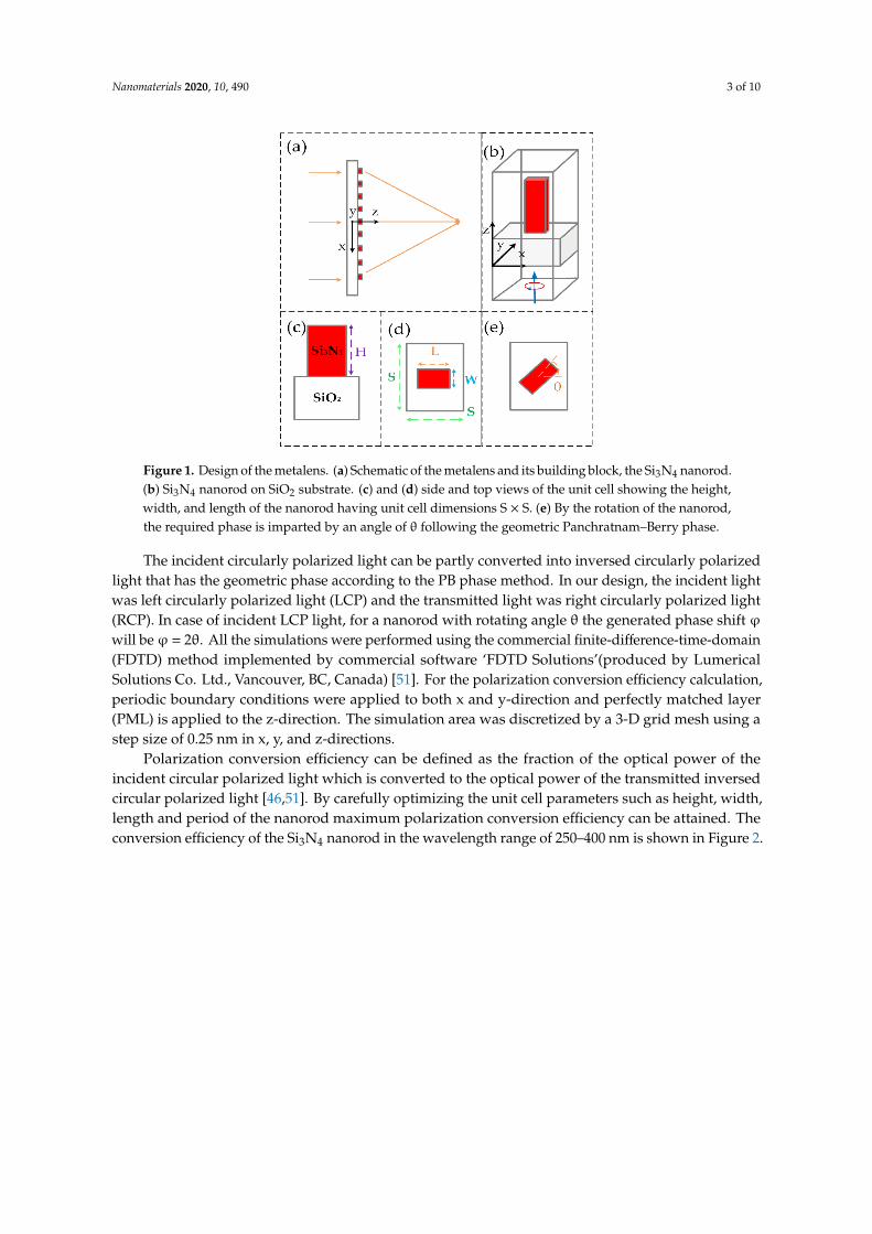
Figure 1. Design of the metalens. (a) Schematic of the metalens and its building block, the Si N nanorod. (b) Si3N4 nanorod on SiO2 substrate. (c) and (d) side and top views of the unit cell showing the height, width, and length of the nanorod having unit cell dimensions S × S. (e) By the rotation of the nanorod, the required phase is imparted by an angle of θ following the geometric Panchratnam–Berry phase.
The incident circularly polarized light can be partly converted into inversed circularly polarized light that has the geometric phase according to the PB phase method. In our design, the incident light was left circularly polarized light (LCP) and the transmitted light was right circularly polarized light (RCP). In case of incident LCP light, for a nanorod with rotating angle θ the generated phase shift φ will be φ = 2θ. All the simulations were performed using the commercial finite-difference-time-domain (FDTD) method implemented by commercial software ‘FDTD Solutions’(produced by Lumerical Solutions Co. Ltd., Vancouver, BC, Canada) [51]. For the polarization conversion efficiency calculation, periodic boundary conditions were applied to both x and y-direction and perfectly matched layer (PML) is applied to the z-direction. The simulation area was discretized by a 3-D grid mesh using a step size of 0.25 nm in x, y, and z-directions.
Polarization conversion efficiency can be defined as the fraction of the optical power of the incident circular polarized light which is converted to the optical power of the transmitted inversed circular polarized light [46,51]. By carefully optimizing the unit cell parameters such as height, width, length and period of the nanorod maximum polarization conversion efficiency can be attained. The conversion efficiency of the Si3N4 nanorod in the wavelength range of 250–400 nm is shown in Figure 2.
Figure 1. Design of the metalens. (a) Schematic of the metalens and its building block, the Si3N4 nanorod.(b) Si3N4 nanorod on SiO2 substrate. (c) and (d) side and top views of the unit cell showing the height,width, and length of the nanorod having unit cell dimensions S × S. (e) By the rotation of the nanorod,the required phase is imparted by an angle of θ following the geometric Panchratnam–Berry phase.
The incident circularly polarized light can be partly converted into inversed circularly polarizedlight that has the geometric phase according to the PB phase method. In our design, the incident lightwas left circularly polarized light (LCP) and the transmitted light was right circularly polarized light(RCP). In case of incident LCP light, for a nanorod with rotating angle θ the generated phase shift ϕwill beϕ = 2θ. All the simulations were performed using the commercial finite-difference-time-domain(FDTD) method implemented by commercial software ‘FDTD Solutions’(produced by LumericalSolutions Co. Ltd., Vancouver, BC, Canada) [51]. For the polarization conversion efficiency calculation,periodic boundary conditions were applied to both x and y-direction and perfectly matched layer(PML) is applied to the z-direction. The simulation area was discretized by a 3-D grid mesh using astep size of 0.25 nm in x, y, and z-directions.
Polarization conversion efficiency can be defined as the fraction of the optical power of theincident circular polarized light which is converted to the optical power of the transmitted inversedcircular polarized light [46,51]. By carefully optimizing the unit cell parameters such as height, width,length and period of the nanorod maximum polarization conversion efficiency can be attained. Theconversion efficiency of the Si3N4 nanorod in the wavelength range of 250–400 nm is shown in Figure 2.
Nanomaterials 2020, 10, 490 4 of 10Nanomaterials 2020, 10, x FOR PEER REVIEW 4 of 10
Figure 2. (a) Simulated polarization conversion efficiency as a function of wavelength for which periodic boundary conditions were applied in x and y directions and perfectly matched layer boundary conditions were applied in the z-direction. (b) Polarization conversion efficiency as a function of wavelength and length of the nanorod at width, W = 85 nm (c) Polarization conversion efficiency as a function of the wavelength and width of the nanorod at length, L = 95 nm.
The polarization conversion efficiency is as high as 96%. The optimized structure parameters for the unit cell are height H = 210 nm, width W = 85 nm, length L = 95 nm, and period S × S = 240 nm.
3. Design of the Metalens, Results, and Discussion
PB phase method was implemented for designing the broadband UV metalens for light convergence at a broadband range of UV light (i.e., 250–400 nm). The incident light with the wavelength λ is focused to a spot by phase control. For a traditional spherical lens, the difference of refractive index between the different media generates the phase shift. As the light propagates through the surface of metalens to the focal point, different positions in the metalens lead to different optical path difference which has a phase shift relative to the center of the metalens (i.e., [51–53]).
2 2 2( , ) ( )x y f f x y= − + +2πφλ
(1)
where, x and y are the coordinates of the nanorod in the metalens, f is the focal length and λ is the wavelength. As the wavelength and the focal length have been determined, the phase φ(x,y) for each nanorod can be calculated. This phase profile is imparted by the rotation of each nanorod at a given coordinate (x,y) by an angle θ(x,y). According to the Pancharatnam–Berry phase method, the phase shift generated by the rotation of the nanorod at the (x,y) position of the metalens has a relationship as [51–53]
( , ) 2 ( , )x y x y=φ θ (2)
where, θ(x,y) is the rotating angle of the nanorod in the position (x,y), hence each nanorod in the metalens is rotated by an angle of [51–53]
2 2 2( , ) ( )x y f f x y= − + +πθλ
(3)
According to the above equation, the rotation angle of all the nanorods is determined at each position. It should be noted that the rotation angle can be an arbitrary value from 0 to π, so the optimized nanorod structure could be able to alter the phase profile of transmitted light at will. Therefore, the transmitted PB phase can achieve full 0 to 2π phase range. The optimized structure
Figure 2. (a) Simulated polarization conversion efficiency as a function of wavelength for whichperiodic boundary conditions were applied in x and y directions and perfectly matched layer boundaryconditions were applied in the z-direction. (b) Polarization conversion efficiency as a function ofwavelength and length of the nanorod at width, W = 85 nm (c) Polarization conversion efficiency as afunction of the wavelength and width of the nanorod at length, L = 95 nm.
The polarization conversion efficiency is as high as 96%. The optimized structure parameters forthe unit cell are height H = 210 nm, width W = 85 nm, length L = 95 nm, and period S × S = 240 nm.
3. Design of the Metalens, Results, and Discussion
PB phase method was implemented for designing the broadband UV metalens for light convergenceat a broadband range of UV light (i.e., 250–400 nm). The incident light with the wavelength λ is focusedto a spot by phase control. For a traditional spherical lens, the difference of refractive index betweenthe different media generates the phase shift. As the light propagates through the surface of metalensto the focal point, different positions in the metalens lead to different optical path difference which hasa phase shift relative to the center of the metalens (i.e., [51–53]).
ϕ(x, y) =2πλ( f −
√f 2 + x2 + y2) (1)
where, x and y are the coordinates of the nanorod in the metalens, f is the focal length and λ is thewavelength. As the wavelength and the focal length have been determined, the phase ϕ(x,y) for eachnanorod can be calculated. This phase profile is imparted by the rotation of each nanorod at a givencoordinate (x,y) by an angle θ(x,y). According to the Pancharatnam–Berry phase method, the phaseshift generated by the rotation of the nanorod at the (x,y) position of the metalens has a relationshipas [51–53]
ϕ(x, y) = 2θ(x, y) (2)
where, θ(x,y) is the rotating angle of the nanorod in the position (x,y), hence each nanorod in themetalens is rotated by an angle of [51–53]
θ(x, y) =π
λ( f −
√f 2 + x2 + y2) (3)
Nanomaterials 2020, 10, 490 5 of 10
According to the above equation, the rotation angle of all the nanorods is determined at eachposition. It should be noted that the rotation angle can be an arbitrary value from 0 to π, so theoptimized nanorod structure could be able to alter the phase profile of transmitted light at will.Therefore, the transmitted PB phase can achieve full 0 to 2π phase range. The optimized structureparameters for the designed metalens in the wavelength range 250–400 nm were chosen as heightH = 340 nm, width W = 85 nm, length L = 150 nm, and period S × S = 240 nm. The diameter of themetalens was 10 µm. The NA of the metalens at the design wavelength λd = 300 nm was calculated tobe 0.75. While focusing, efficiency of the metalens was as high as 77%. Figure 3 presents the focusingcharacteristics of the designed metalens.
Nanomaterials 2020, 10, x FOR PEER REVIEW 5 of 10
parameters for the designed metalens in the wavelength range 250–400 nm were chosen as height H = 340 nm, width W = 85 nm, length L = 150 nm, and period S × S = 240 nm. The diameter of the metalens was 10 µm. The NA of the metalens at the design wavelength λd = 300 nm was calculated to be 0.75. While focusing, efficiency of the metalens was as high as 77%. Figure 3 presents the focusing characteristics of the designed metalens.
Figure 3. Focusing characteristics of UV metalense at incident UV light 250–400 nm. Normalized intensity distribution at y-z plane at (a) λ = 250 nm, (b) λ = 300 nm, (c) λ = 350 nm and (d) λ = 400 nm. Normalized intensity distribution of the metalens at x-y plane at x = y = 0. (e) λ = 250 nm along x-axis at z = 5.3 µm, (f) λ = 300 nm, along x-axis at z = 4.4 µm (g) λ = 350 nm, along x-axis at z = 3.5 µm and (h) λ = 400 nm, along x-axis at z = 2.9 µm. The metalens has a diameter of 10 µm, the numerical aperture (NA) of the metalens at designed wavelength λd = 300 nm is 0.75.
The normalized intensity distributions of the transmitted light beam in the y-z section of the metalens are shown in Figure 3a–d and the intensity profiles of the transmitted light beam in the x-y section of the metalens are shown in Figure 3e–h. The intensity distribution of the focal spot exhibits a strongly focused, bright, and symmetric spot at the center of the focal plane at respective wavelengths (250 nm, 300 nm, 350 nm, and 400 nm). The corresponding normalized intensity profiles along the x-axis show a sharp peak at the center of the plane as shown in Figure 4.
Figure 3. Focusing characteristics of UV metalense at incident UV light 250–400 nm. Normalizedintensity distribution at y-z plane at (a) λ = 250 nm, (b) λ = 300 nm, (c) λ = 350 nm and (d) λ = 400 nm.Normalized intensity distribution of the metalens at x-y plane at x = y = 0. (e) λ = 250 nm along x-axisat z = 5.3 µm, (f) λ = 300 nm, along x-axis at z = 4.4 µm (g) λ = 350 nm, along x-axis at z = 3.5 µmand (h) λ = 400 nm, along x-axis at z = 2.9 µm. The metalens has a diameter of 10 µm, the numericalaperture (NA) of the metalens at designed wavelength λd = 300 nm is 0.75.
The normalized intensity distributions of the transmitted light beam in the y-z section of themetalens are shown in Figure 3a–d and the intensity profiles of the transmitted light beam in the x-ysection of the metalens are shown in Figure 3e–h. The intensity distribution of the focal spot exhibits astrongly focused, bright, and symmetric spot at the center of the focal plane at respective wavelengths(250 nm, 300 nm, 350 nm, and 400 nm). The corresponding normalized intensity profiles along thex-axis show a sharp peak at the center of the plane as shown in Figure 4.
Nanomaterials 2020, 10, 490 6 of 10
Nanomaterials 2020, 10, x FOR PEER REVIEW 5 of 10
parameters for the designed metalens in the wavelength range 250–400 nm were chosen as height H = 340 nm, width W = 85 nm, length L = 150 nm, and period S × S = 240 nm. The diameter of the metalens was 10 µm. The NA of the metalens at the design wavelength λd = 300 nm was calculated to be 0.75. While focusing, efficiency of the metalens was as high as 77%. Figure 3 presents the focusing characteristics of the designed metalens.
Figure 3. Focusing characteristics of UV metalense at incident UV light 250–400 nm. Normalized intensity distribution at y-z plane at (a) λ = 250 nm, (b) λ = 300 nm, (c) λ = 350 nm and (d) λ = 400 nm. Normalized intensity distribution of the metalens at x-y plane at x = y = 0. (e) λ = 250 nm along x-axis at z = 5.3 µm, (f) λ = 300 nm, along x-axis at z = 4.4 µm (g) λ = 350 nm, along x-axis at z = 3.5 µm and (h) λ = 400 nm, along x-axis at z = 2.9 µm. The metalens has a diameter of 10 µm, the numerical aperture (NA) of the metalens at designed wavelength λd = 300 nm is 0.75.
The normalized intensity distributions of the transmitted light beam in the y-z section of the metalens are shown in Figure 3a–d and the intensity profiles of the transmitted light beam in the x-y section of the metalens are shown in Figure 3e–h. The intensity distribution of the focal spot exhibits a strongly focused, bright, and symmetric spot at the center of the focal plane at respective wavelengths (250 nm, 300 nm, 350 nm, and 400 nm). The corresponding normalized intensity profiles along the x-axis show a sharp peak at the center of the plane as shown in Figure 4.
Figure 4. Normalized intensity profiles of the focus spot along x-direction at respective wavelengths(a) y = 0, λ = 250 nm, z = 5.3 µm, (b) y = 0, λ = 300 nm, z = 4.4 µm, (c) y = 0, λ = 350 nm, z = 3.5 µm and(d) y = 0, λ = 400 nm, z = 2.9 µm.
The focal length of the metalens was measured at representative wavelengths (250 nm, 300 nm,350 nm, and 400 nm). The calculated full width at half maximum (FWHM) of the focal spots at therespective wavelengths was 206 nm, 210 nm, 226 nm, and 238 nm; all the values were diffraction-limited(i.e., λd
2NA ). The normalized intensity profiles of the focal spot along x-direction (at z = f, and y = 0)are shown in Figure 4. The focusing efficiency of the UV metalens is measured to be as high as 77%,shown in Figure 5.
Nanomaterials 2020, 10, x FOR PEER REVIEW 6 of 10
Figure 4. Normalized intensity profiles of the focus spot along x-direction at respective wavelengths (a) y = 0, λ = 250 nm, z = 5.3 µm, (b) y = 0, λ = 300 nm, z = 4.4 µm, (c) y = 0, λ = 350 nm, z = 3.5 µm and (d) y = 0, λ = 400 nm, z = 2.9 µm.
The focal length of the metalens was measured at representative wavelengths (250 nm, 300 nm, 350 nm, and 400 nm). The calculated full width at half maximum (FWHM) of the focal spots at the respective wavelengths was 206 nm, 210 nm, 226 nm, and 238 nm; all the values were diffraction-
limited (i.e.2NA
dλ ). The normalized intensity profiles of the focal spot along x-direction (at z = f, and y
= 0) are shown in Figure 4. The focusing efficiency of the UV metalens is measured to be as high as 77%, shown in Figure 5.
.
Figure 5. Focusing efficiency of the metalens designed for the broadband UV spectrum 250–400 nm.
We verified four wavelengths during the optimizing process; the designed metalens worked quite well over the broadband range of 250–400 nm.
We also examined the focusing characteristics of the designed metalens at different incident angles (i.e., 5°, 15°, and 25°). It can be seen by the simulation results presented in Figure 6 that the transmitted light beam was clear. Figure 6 shows the focusing characteristics and corresponding normalized intensity distribution of the focal spot at different incident angles at the respective wavelengths.
Figure 5. Focusing efficiency of the metalens designed for the broadband UV spectrum 250–400 nm.
We verified four wavelengths during the optimizing process; the designed metalens worked quitewell over the broadband range of 250–400 nm.
We also examined the focusing characteristics of the designed metalens at different incident angles(i.e., 5◦, 15◦, and 25◦). It can be seen by the simulation results presented in Figure 6 that the transmittedlight beam was clear. Figure 6 shows the focusing characteristics and corresponding normalizedintensity distribution of the focal spot at different incident angles at the respective wavelengths.
Nanomaterials 2020, 10, 490 7 of 10Nanomaterials 2020, 10, x FOR PEER REVIEW 7 of 10
Figure 6. Focusing characteristics of UV metalens at 250–400 nm at different incident angles. Normalized intensity distribution at x-z plane at an incident angle of 5° (a) λ = 250 nm, (b) λ = 300 nm, (c) λ = 350 nm and (d) λ = 400 nm. Normalized intensity distribution of the metalens at x-z plane at an incident angle of 15° (e) λ = 250 nm, (f) λ = 300 nm (g) λ = 350 nm and (h) λ = 400 nm. Normalized intensity distribution at x-z plane at an incident angle of 25° (i) λ = 250 nm (j) λ = 300 nm (k) λ = 350 nm and (l) λ = 400 nm
4. Conclusions
In summary, we report the design of a dielectric, high efficiency, diffraction-limited UV metalens based on silicon nitride metasurface functioning in the broadband spectrum of ultraviolet light (i.e., from 250–400 nm). PB phase was implemented to the unit cell to realize the required phase distribution of the metalens. The simulated conversion efficiency was 96% while the focusing efficiency of the metalens was as high as 77%. We also investigated the focusing characteristics of the metalens at different incident angles (i.e. 5°, 15°, and 25°), which showed a clear focus spot. The designed UV metalens can have a great promising perception for a diverse range of applications in lithography, UV laser, UV directional light, image sensors, sterilization, communication, and so on. This research on high efficiency broadband UV metalenses can pave the way towards the advancement of miniaturized and integrated UV nanophotonics. Techniques like multiple couple resonances, tailoring the phase profiles at numerous distinct UV wavelengths, engineering the dispersion, or stacking metasurfaces could be adopted in the future for designing an achromatic UV metalens.
Author Contributions: S.K conceived and designed the experiments, and wrote the original manuscript; B.Y, D.K, X.C, Y.K, and C.B contributed to the analysis; J.W and D.Z supervised the study and reviewed the manuscript.
Funding: This work is supported by National Science Foundation Project 61775140 and 81701745, National Key R&D Program of China 2018YFA0701800, Shanghai Municipal Science and Technology Commission Innovation Action Plan 18DZ1100400.
Conflicts of Interest: The authors declare no conflict of interest.
References
Figure 6. Focusing characteristics of UV metalens at 250–400 nm at different incident angles. Normalizedintensity distribution at x-z plane at an incident angle of 5◦ (a) λ= 250 nm, (b) λ= 300 nm, (c) λ = 350 nmand (d) λ = 400 nm. Normalized intensity distribution of the metalens at x-z plane at an incidentangle of 15◦ (e) λ = 250 nm, (f) λ = 300 nm (g) λ = 350 nm and (h) λ = 400 nm. Normalized intensitydistribution at x-z plane at an incident angle of 25◦ (i) λ = 250 nm (j) λ = 300 nm (k) λ = 350 nm and(l) λ = 400 nm
4. Conclusions
In summary, we report the design of a dielectric, high efficiency, diffraction-limited UV metalensbased on silicon nitride metasurface functioning in the broadband spectrum of ultraviolet light(i.e., from 250–400 nm). PB phase was implemented to the unit cell to realize the required phasedistribution of the metalens. The simulated conversion efficiency was 96% while the focusing efficiencyof the metalens was as high as 77%. We also investigated the focusing characteristics of the metalens atdifferent incident angles (i.e., 5◦, 15◦, and 25◦), which showed a clear focus spot. The designed UVmetalens can have a great promising perception for a diverse range of applications in lithography, UVlaser, UV directional light, image sensors, sterilization, communication, and so on. This research onhigh efficiency broadband UV metalenses can pave the way towards the advancement of miniaturizedand integrated UV nanophotonics. Techniques like multiple couple resonances, tailoring the phaseprofiles at numerous distinct UV wavelengths, engineering the dispersion, or stacking metasurfacescould be adopted in the future for designing an achromatic UV metalens.
Author Contributions: S.K. conceived and designed the experiments, and wrote the original manuscript; B.Y.,D.K., X.C., Y.K., and C.B. contributed to the analysis; J.W. and D.Z. supervised the study and reviewed themanuscript. All authors have read and agreed to the published version of the manuscript.
Funding: This work is supported by National Science Foundation Project 61775140 and 81701745, National KeyR&D Program of China 2018YFA0701800, Shanghai Municipal Science and Technology Commission InnovationAction Plan 18DZ1100400.
Conflicts of Interest: The authors declare no conflict of interest.
References
1. Mueller, J.B.; Rubin, N.A.; Devlin, R.C.; Groever, B.; Capasso, F. Metasurface polarization optics: Independentphase control of arbitrary orthogonal states of polarization. Phys. Rev. Lett. 2017, 118, 113901. [CrossRef][PubMed]
2. Khorasaninejad, M.; Shi, Z.; Zhu, A.Y.; Chen, W.-T.; Sanjeev, V.; Zaidi, A.; Capasso, F. Achromatic metalensover 60 nm bandwidth in the visible and metalens with reverse chromatic dispersion. Nano Lett. 2017, 17,1819–1824. [CrossRef] [PubMed]
launcher. Adv. Funct. Mater. 2018, 28, 1705503. [CrossRef]5. Ahmadivand, A.; Gerislioglu, B.; Ramezani, Z. Gated graphene island-enabled tunable charge transfer
plasmon terahertz metamodulator. Nanoscale 2019, 11, 8091–8095. [CrossRef]6. Yu, B.; Wen, J.; Chen, X.; Zhang, D. An achromatic metalens in the near-infrared region with an array based
on a single nano-rod unit. Appl. Phys. Express 2019, 12, 092003. [CrossRef]7. Bai, W.; Yang, P.; Wang, S.; Huang, J.; Chen, D.; Zhang, Z.; Yang, J.; Xu, B. Tunable duplex metalens based on
phase-change materials in communication range. Nanomaterials 2019, 9, 993. [CrossRef]8. Liang, Y.; Liu, H.; Wang, F.; Meng, H.; Guo, J.; Li, J.; Wei, Z. High-efficiency, near-diffraction limited, dielectric
metasurface lenses based on crystalline titanium dioxide at visible wavelengths. Nanomaterials 2018, 8, 288.[CrossRef]
13. Zhang, M.; Pu, M.; Zhang, F.; Guo, Y.; He, Q.; Ma, X.; Huang, Y.; Li, X.; Yu, H.; Luo, X. Plasmonic metasurfacesfor switchable photonic spin–orbit interactions based on phase change materials. Adv. Sci. 2018, 5, 1800835.[CrossRef] [PubMed]
14. De Galarreta, C.R.; Alexeev, A.M.; Au, Y.Y.; Lopez-Garcia, M.; Klemm, M.; Cryan, M.; Bertolotti, J.;Wright, C.D. Nonvolatile reconfigurable phase-change metadevices for beam steering in the near infrared.Adv. Funct. Mater. 2018, 28, 1704993. [CrossRef]
19. Chen, W.T.; Zhu, A.Y.; Sanjeev, V.; Khorasaninejad, M.; Shi, Z.; Lee, E.; Capasso, F. A broadband achromaticmetalens for focusing and imaging in the visible. Nat. Nanotechnol. 2018, 13, 220–226. [CrossRef]
26. Jakšic, Z.; Vukovic, S.; Matovic, J.; Tanaskovic, D. Negative refractive index metasurfaces for enhancedbiosensing. Materials 2011, 4, 1–36. [CrossRef]
27. Ahmadivand, A.; Gerislioglu, B.; Manickam, P.; Kaushik, A.; Bhansali, S.; Nair, M.; Pala, N. Rapid detectionof infectious envelope proteins by magnetoplasmonic toroidal metasensors. ACS Sens. 2017, 2, 1359–1368.[CrossRef]
28. Chizari, A.; Abdollahramezani, S.; Jamali, M.V.; Salehi, J.A. Analog optical computing based on a dielectricmeta-reflect array. Opt. Lett. 2016, 41, 3451–3454. [CrossRef]
47. Devlin, R.C.; Khorasaninejad, M.; Chen, W.T.; Oh, J.; Capasso, F. Broadband high-efficiency dielectricmetasurfaces for the visible spectrum. Proc. Natl. Acad. Sci. USA 2016, 113, 10473–10478. [CrossRef][PubMed]