Page 1
HIGH EFFICIENCY, LOW COST FULLYINTEGRATED DC-DC CONVERTER SOLUTION
A DISSERTATION
SUBMITTED TO THE FACULTY OF THE GRADUATE SCHOOL
OF THE UNIVERSITY OF MINNESOTA
BY
SUDHIR S. KUDVA
IN PARTIAL FULFILLMENT OF THE REQUIREMENTS
FOR THE DEGREE OF
Doctor of Philosophy
PROF. RAMESH HARJANI
April, 2013
Page 2
c© SUDHIR S. KUDVA 2013
ALL RIGHTS RESERVED
Page 3
Acknowledgements
There are many people who have helped, supported and guided me to reach this juncture
in my life and this thesis will be incomplete without offering my gratitude to them.
Firstly, I would like to express my gratitude to Prof. Ramesh Harjani for giving me
the opportunity to work in his lab and guiding me through my PhD. I am extremely
thankful for the freedom he provided me to pursue the research way I liked. But
nevertheless he always knew what I did and advised me when he felt I was spending
too much time on something unreasonable or chasing something unachievable. From
my conversations with my friends in other universities, I have realized that I have been
very lucky in terms of number of tape-outs and the testing facilities at my disposal. I
am indebted to Prof. Harjani for making these facilities available to us and not have
to worry about these things. I have not only benefited technically but also learnt many
other skills such as technical writing, making quality presentations and proposal writing.
I will miss the get togethers, parties at Prof. Harjani’s house and lively discussion I
used to have with Savita ma’am on topics ranging from Indian politics to US law.
I would like to thank Prof. Ned Mohan for agreeing to chair my defense and pre-
liminary oral committee. I would also like to thank Prof. Chris Kim and Prof. Richard
Moeckel for agreeing to be the part of my defense and preliminary oral committee. The
comments given by the committee during the preliminary oral exam were very insight-
ful and helpful towards the latter half of my PhD. I am also thankful to Prof. Anand
i
Page 4
Gopinath and Prof. Paul Imbertson for giving me the opportunity to be a teaching
assistant for their courses. They were both great teachers and made me realize how
much effort goes in teaching a course.
During my PhD there were many instances where I felt something was not possible
to achieve within the deadline and my lab mates were always there to pitch in and make
the impossible possible. In spite of their busy schedule, they were always ready to take
time out for me when I needed any help. I am indebted to Satwik for helping me with
any doubts related to circuit design, debugging tool related issues, providing a helping
hand during the tape outs, teaching me how to play tennis, helping me out when I went
for an internship at Intel, Hillsboro and introducing me to some colorful lingo which has
now become part of my lexicon. I am thankful to Bodhi for the long discussions we had
both technical and non-technical, being my gym coach and above all being there for me
every time I needed some advise, no matter what the topic was. I also miss the idle chats
and mutual cribbing sessions we had together. I am indebted to Martin for teaching
me how to solder, operate some of the test equipments and debugging during testing. I
was privileged to work and share chip space with Taehyoun, Jaehyup and Mohammad.
I am grateful to them for sharing the intense workload during the tape outs. Ashutosh
and Sachin were not only great lab mates but even greater friends. There was never a
dull moment with these two guys around. Thanks Lanka saab for giving me some of
the valuable life lessons in his inimitable style. I am also thankful to Rakesh Palani,
Mustafijur Rahman, Kin-Joe Sham, Mahmoud Reza Ahmadi and Shriharsh Vadlamani.
I am indebted Prof. Sumam David, my adviser for bachelors project and Prof.
Bharadwaj Amrutur, my master’s adviser for imbibing in me a spirit of research and
motivating me to apply for a PhD.
I am grateful to Semiconductor Research corporation (SRC) for supporting my
project. I am thankful to all my SRC mentors Tanay Karnik, Ram Krishnamurthy,
ii
Page 5
Mohammad Khellah, Jeff Cunningham, Bruce Fleischer, Pong-Fei Lu and Koushik K.
Das. Some of their comments and directions they provided played a major role in
shaping this project.
I learnt a lot during my two internships at Intel. I was able to imbibe some of the
design methodology and practices that ensure the success of design in my project as
well. I am indebted to my managers Richard Forand, Krishnan Ravichandran, John
Critchlow and Wu Zuoguo for giving me an opportunity to work in their group. I am
also thankful to my mentors Rinkle Jain, Mohiuddin Mazumdar and Arvind at Intel. I
would also like to thank my team-mates in Intel Harish and George.
There are many people in the ECE department who silently work behind the scenes
and ensure that we students always have the best possible facilities. They ensure that
we spend minimum time on the administrative work and focus most of the time on
our research. I would like to thank Carlos Soria, Chimai Nguyen, Dan Dobrick, Becky
Colberg, Linda Jagerson, Kyle Dukart, Jim Aufderhar, Paula Beck and Linda Bullis.
Outside the lab, many people helped me when I came to Minneapolis. I am thankful
to my first year room-mates Sourabh and Sujit for initiating me to the US lifestyle and
teaching me the necessary survival skills for facing the Minnesota winter. I am also
thankful to my other room-mates Vivek and Rohit for putting up with my random time
schedule and not complaining once about it. I will always cherish the fun time that I
had with Sourabh and Sunayana, be it a trips to Duluth or shopping spree in Albertville
or grocery shopping trips late at night. And special thanks to Sunayana for teaching me
the art of ”saving” money by shopping. I would also like to thank Sauptik for making
me run around badiminton court and being my doubles partner in badminton knowing
well that defeat is certain. Thanks Vandana didi for taking my side against Lanka saab
and for some wonderful authentic Gult food.
I am blessed with great friends, who were always there for me. They raised my
iii
Page 6
spirits whenever I felt down and I had some of the best time with them. I would like
take this opportunity to thank Varad, Tejeswini, Vasuki, Ranjani, Sandeep, Shruti,
Aditya, Subramanya, Jagdish, Harisha, Saikiran and Chaitanya.
Finally, I will be ever grateful to my parents for believing in me and supporting me
in every endeavor that I undertook. They always ensured the best for me and gave
me all the freedom to do what I liked the most. My brother has been the pillar of
strength and has always stood by me in spite of me getting angry at him sometimes.
In Nanditha, I have not only found a good wife but a very understanding person and a
awesome friend. She always figured out when I was stressed and came up with ways to
make me feel good again.
Thank you.
iv
Page 7
Dedicated to my parents, my brother
and my wife Nandu
v
Page 8
Abstract
Rapid advances in the field of integrated circuit design has been advantageous from
point of view of cost and miniaturization. However, power dissipation in highly inte-
grated digital systems has become a major cause of concern. One of the methods to
reduce power dissipation is to dynamically vary the supply voltage (DVS) of digital
block depending on the load conditions. This requires high efficiency power converters
to dynamically vary the supply voltage. Taking this a step further, the digital system
can be further sub-divided into multiple independent voltage domains and DVS applied
independently to these voltage domains. To economically support such an implementa-
tion fully integrated on-chip power converters are a way forward.
This thesis focuses on the design of fully integrated power converters to support DVS
type applications. A switched inductive type converter is highly efficient as its efficiency
depends only on the parasitics. But, a fully integrated switched inductive converter has
some drawbacks and fails to support wide output power range. To circumvent the
problem, we have implemented a switched inductive converter that operates in different
modes based on the load that the converter supports. In these modes of operation,
either the power switch size is scaled or the frequency is scaled to cut down the losses
in the converter. The design achieves a peak efficiency of 74.5% and supplies a 450x
output power range (0.6mW to 266mW).
A fully integrated capacitive converter with all digital ripple mitigation aimed at
supporting the lower output power ranges has been designed. The capacitive converter
uses a dual loop control, where a single bound hysteretic control loop achieves regulation
and the secondary loop achieves ripple control by modulating capacitance size and
charge/discharge time of the capacitance used to transfer charge from the input to
vi
Page 9
output. The partial charge/discharge technique used to achieve ripple control does not
degrade the efficiency, has been proved both theoretically and experimentally. The
design taped out in IBM 130nm process achieves a maximum efficiency of 70% and
reduces the measured ripple from 98mV to 30mV at 0.3V and 4mA load current.
A test-chip designed to study the impact of placing digital circuits underneath
inductor used in power converter type applications is presented. The experimental
results show the feasibility of implementing digital circuits underneath the inductor,
thereby achieving higher area efficiency for the converter. Finally, a combined induc-
tive/capacitive converter where the inductive converter supports the higher power range
and capacitive converter supports the lower power ranges is described. The combined
converter taped out in IBM 32nm SOI process achieves a maximum efficiency of 85.5%
and a power density of 0.7W/mm2.
Additionally, we have also proposed a passive resonance reduction technique to re-
duce resonance on the supply line in bondwire based packages. The technique utilizes
the area underneath the bondpad to implement passives required for resonance reduc-
tion.
vii
Page 10
Contents
Acknowledgements i
Abstract vi
List of Tables xii
List of Figures xiii
1 Introduction 1
1.1 Applications . . . . . . . . . . . . . . . . . . . . . . . . . . . . . . . . . . 7
1.2 Types of Converter . . . . . . . . . . . . . . . . . . . . . . . . . . . . . . 9
1.3 Organization . . . . . . . . . . . . . . . . . . . . . . . . . . . . . . . . . 10
2 Inductive converter 12
2.1 Introduction . . . . . . . . . . . . . . . . . . . . . . . . . . . . . . . . . . 12
2.2 Buck converter . . . . . . . . . . . . . . . . . . . . . . . . . . . . . . . . 14
2.3 Switch scaling and frequency scaling architecture . . . . . . . . . . . . . 16
2.3.1 Switch Scaling . . . . . . . . . . . . . . . . . . . . . . . . . . . . 18
2.3.2 Frequency Scaling . . . . . . . . . . . . . . . . . . . . . . . . . . 21
2.3.3 Integrated converter . . . . . . . . . . . . . . . . . . . . . . . . . 22
2.4 Additional converter features . . . . . . . . . . . . . . . . . . . . . . . . 24
viii
Page 11
2.4.1 Load Current Detection and State Machine . . . . . . . . . . . . 24
2.4.2 PWM transient speed up . . . . . . . . . . . . . . . . . . . . . . 25
2.4.3 Passives . . . . . . . . . . . . . . . . . . . . . . . . . . . . . . . . 26
2.5 Measurement results . . . . . . . . . . . . . . . . . . . . . . . . . . . . . 27
2.5.1 Efficiency . . . . . . . . . . . . . . . . . . . . . . . . . . . . . . . 28
2.5.2 Transient response . . . . . . . . . . . . . . . . . . . . . . . . . . 33
2.5.3 Effect of temperature . . . . . . . . . . . . . . . . . . . . . . . . 35
2.6 Comparison with previous work . . . . . . . . . . . . . . . . . . . . . . . 36
2.7 Summary . . . . . . . . . . . . . . . . . . . . . . . . . . . . . . . . . . . 39
3 Capacitive converter 41
3.1 Introduction . . . . . . . . . . . . . . . . . . . . . . . . . . . . . . . . . . 41
3.2 Capacitive converter model . . . . . . . . . . . . . . . . . . . . . . . . . 45
3.3 Efficiency and Loss components . . . . . . . . . . . . . . . . . . . . . . . 46
3.4 Partial Charging/Discharging and Efficiency . . . . . . . . . . . . . . . . 50
3.5 Implementation . . . . . . . . . . . . . . . . . . . . . . . . . . . . . . . 56
3.5.1 Converter core and primary control loop . . . . . . . . . . . . . . 56
3.5.2 Secondary ripple control loop . . . . . . . . . . . . . . . . . . . . 58
3.5.3 Pulse width variation in hysteretic environment . . . . . . . . . . 60
3.5.4 Passives and load . . . . . . . . . . . . . . . . . . . . . . . . . . . 61
3.6 Measurement Results . . . . . . . . . . . . . . . . . . . . . . . . . . . . . 62
3.7 Summary . . . . . . . . . . . . . . . . . . . . . . . . . . . . . . . . . . . 73
4 Inductors Above Digital Circuits for Compact On-Chip Switching
Regulators 74
4.1 Introduction . . . . . . . . . . . . . . . . . . . . . . . . . . . . . . . . . . 74
4.2 Test-chip and experimental setup . . . . . . . . . . . . . . . . . . . . . . 76
ix
Page 12
4.3 Effect of Low Resistivity Substrate . . . . . . . . . . . . . . . . . . . . . 77
4.4 Coupling from Digital Circuits to Inductor . . . . . . . . . . . . . . . . . 77
4.5 Coupling from Inductor to Digital Circuits . . . . . . . . . . . . . . . . . 79
4.6 Summary . . . . . . . . . . . . . . . . . . . . . . . . . . . . . . . . . . . 83
5 Combined Inductive/Capacitive Converter 84
5.1 Introduction . . . . . . . . . . . . . . . . . . . . . . . . . . . . . . . . . . 84
5.2 Inductive converter . . . . . . . . . . . . . . . . . . . . . . . . . . . . . . 85
5.2.1 Analog to Digital converter (ADC) . . . . . . . . . . . . . . . . . 86
5.2.2 Accumulator . . . . . . . . . . . . . . . . . . . . . . . . . . . . . 89
5.2.3 Digital Pulse Width Modulator . . . . . . . . . . . . . . . . . . . 90
5.2.4 Passives . . . . . . . . . . . . . . . . . . . . . . . . . . . . . . . . 91
5.2.5 Efficiency Improvement Techniques . . . . . . . . . . . . . . . . . 92
5.3 Capacitive converter . . . . . . . . . . . . . . . . . . . . . . . . . . . . . 93
5.4 Combined converter architecture . . . . . . . . . . . . . . . . . . . . . . 94
5.5 Simulation results . . . . . . . . . . . . . . . . . . . . . . . . . . . . . . 97
5.6 Combined converter with increased area efficiency . . . . . . . . . . . . 102
5.7 Test Setup . . . . . . . . . . . . . . . . . . . . . . . . . . . . . . . . . . . 103
5.7.1 Steady state efficiency . . . . . . . . . . . . . . . . . . . . . . . . 103
5.7.2 Load transient measurement . . . . . . . . . . . . . . . . . . . . 105
5.7.3 Transient measurement . . . . . . . . . . . . . . . . . . . . . . . 105
5.8 Summary . . . . . . . . . . . . . . . . . . . . . . . . . . . . . . . . . . . 106
6 Supply Resonance Reduction Technique 108
6.1 Introduction . . . . . . . . . . . . . . . . . . . . . . . . . . . . . . . . . . 108
6.2 Previous Work . . . . . . . . . . . . . . . . . . . . . . . . . . . . . . . . 110
6.3 Theory of Passive Resonance Cancellation . . . . . . . . . . . . . . . . . 111
x
Page 13
6.3.1 ωpar = ωser . . . . . . . . . . . . . . . . . . . . . . . . . . . . . . 112
6.3.2 ωpar < ωser . . . . . . . . . . . . . . . . . . . . . . . . . . . . . . 112
6.4 Experiment Setup and Simulation Results . . . . . . . . . . . . . . . . . 115
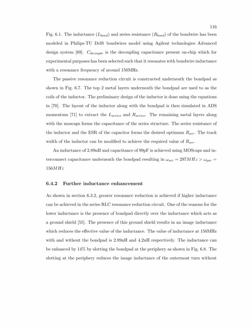
6.4.1 Design, Modeling and parameter extraction . . . . . . . . . . . . 115
6.4.2 Further inductance enhancement . . . . . . . . . . . . . . . . . . 116
6.5 Summary . . . . . . . . . . . . . . . . . . . . . . . . . . . . . . . . . . . 117
7 Conclusions & Contributions 120
7.1 Future work . . . . . . . . . . . . . . . . . . . . . . . . . . . . . . . . . . 122
References 123
xi
Page 14
List of Tables
2.1 Switching + controller power in different modes . . . . . . . . . . . . . . 33
2.2 Comparison with prior work . . . . . . . . . . . . . . . . . . . . . . . . . 37
2.3 Design summary . . . . . . . . . . . . . . . . . . . . . . . . . . . . . . . 39
3.1 Comparison with prior work . . . . . . . . . . . . . . . . . . . . . . . . . 72
3.2 Design summary . . . . . . . . . . . . . . . . . . . . . . . . . . . . . . . 72
5.1 Area occupied by the converter components . . . . . . . . . . . . . . . . 97
5.2 Power density of converters . . . . . . . . . . . . . . . . . . . . . . . . . 103
xii
Page 15
List of Figures
1.1 Evolution of mobile phones [1] . . . . . . . . . . . . . . . . . . . . . . . 2
1.2 Heat removal methods used for cooling the CPU . . . . . . . . . . . . . 3
1.3 Water cooling system in Google’s South Carolina center . . . . . . . . . 4
1.4 Regulator fully off-chip on the PCB . . . . . . . . . . . . . . . . . . . . 5
1.5 Regulator with only passives off-chip on the PCB . . . . . . . . . . . . . 6
1.6 Fully integrated converter . . . . . . . . . . . . . . . . . . . . . . . . . . 6
1.7 Components of power in a laptop . . . . . . . . . . . . . . . . . . . . . . 7
1.8 Variation of current, power and frequency with supply voltage . . . . . . 8
2.1 A typical buck converter and % power dissipation vs load power for a
PWM buck . . . . . . . . . . . . . . . . . . . . . . . . . . . . . . . . . . 14
2.2 Constant frequency PWM mode with switch scaling . . . . . . . . . . . 19
2.3 Bode plot for full system matlab simulation of the converter . . . . . . . 20
2.4 Frequency scaling using PFM controller . . . . . . . . . . . . . . . . . . 22
2.5 Integrated converter with switch scaling and frequency scaling . . . . . . 23
2.6 Current detect and state machine for automatic mode change . . . . . . 25
2.7 PWM speedup circuit and decision circuit algorithm . . . . . . . . . . . 26
2.8 Stacked inductor and chip microphotograph of wide output range DC-DC
converter . . . . . . . . . . . . . . . . . . . . . . . . . . . . . . . . . . . 27
2.9 Populated printed circuit board used for testing the converter . . . . . . 28
xiii
Page 16
2.10 Efficiency of the converter in PWM and PFM modes for different output
voltages . . . . . . . . . . . . . . . . . . . . . . . . . . . . . . . . . . . . 29
2.11 Converter efficiency for different switching frequencies Vout=860mV . . 29
2.12 VI profile of ring oscillator and efficiency of the converter for the VI
profile shown . . . . . . . . . . . . . . . . . . . . . . . . . . . . . . . . . 30
2.13 Output voltage ripple in PWM and PFM modes . . . . . . . . . . . . . 32
2.14 Transient response in PWM → PWM mode with and without speed-up 33
2.15 Automatic mode change transient response . . . . . . . . . . . . . . . . 34
2.16 Efficiency variation with temperature Vout = 760mV . . . . . . . . . . . 35
3.1 Catalog of ripple control techniques . . . . . . . . . . . . . . . . . . . . . 43
3.2 A simple 1:1 converter and the model of a capacitive converter . . . . . 45
3.3 Variation of maximum load current . . . . . . . . . . . . . . . . . . . . . 47
3.4 Components of Pin . . . . . . . . . . . . . . . . . . . . . . . . . . . . . . 48
3.5 Analytical model for the overall efficiency of the converter for different
loads . . . . . . . . . . . . . . . . . . . . . . . . . . . . . . . . . . . . . . 49
3.6 Effect of partial charging on efficiency . . . . . . . . . . . . . . . . . . . 51
3.7 Effect of partial charging on efficiency for a 2:1 converter . . . . . . . . . 54
3.8 Fully integrated capacitive converter . . . . . . . . . . . . . . . . . . . . 57
3.9 Vm = Vin
2 mode and the effective circuits during the 2 phases of operation 57
3.10 Vm = Vin
3 mode and the effective circuits during the 2 phases of operation 58
3.11 Algorithm implemented in secondary loop . . . . . . . . . . . . . . . . . 59
3.12 Implementation of pulse width modulation in hysteresis environment . . 60
3.13 Die photograph of fully integrated capacitive converter . . . . . . . . . . 62
3.14 PCB used to test the capacitive converter . . . . . . . . . . . . . . . . . 63
3.15 Overall efficiency of the converter . . . . . . . . . . . . . . . . . . . . . . 64
3.16 Core efficiency of the converter . . . . . . . . . . . . . . . . . . . . . . . 65
xiv
Page 17
3.17 Variation of ripple with capacitance and charge/discharge time modulation 67
3.18 Variation of ripple with Vout for Iload = 4mA . . . . . . . . . . . . . . . 68
3.19 Output ripple under different modulation conditions @ Vout = 0.4V ,
Iload = 2mA (AC coupled) . . . . . . . . . . . . . . . . . . . . . . . . . . 68
3.20 Transient response of the converter for reference voltage change . . . . . 69
3.21 Load dependent nature of the downward transition of the output voltage
Iload = 2mA . . . . . . . . . . . . . . . . . . . . . . . . . . . . . . . . . . 70
3.22 Transient measurement for load current change for fixed reference voltage 71
4.1 Inductor over digital logic separated into voltage domains . . . . . . . . 75
4.2 Die micrograph of fabricated test inductors . . . . . . . . . . . . . . . . 76
4.3 Inductance of the inductors . . . . . . . . . . . . . . . . . . . . . . . . . 78
4.4 Series resistance of the inductors . . . . . . . . . . . . . . . . . . . . . . 78
4.5 Ring oscillator output . . . . . . . . . . . . . . . . . . . . . . . . . . . . 79
4.6 Leakage on inductor . . . . . . . . . . . . . . . . . . . . . . . . . . . . . 80
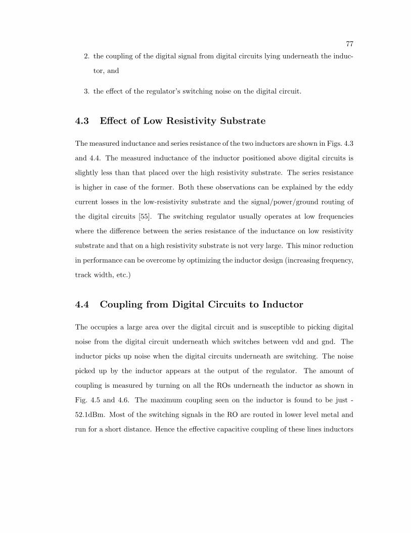
4.7 Coupled power at square wave frequency . . . . . . . . . . . . . . . . . . 81
4.8 Noise paths in a digital circuit . . . . . . . . . . . . . . . . . . . . . . . 82
4.9 Eye diagram of the ring oscillator output . . . . . . . . . . . . . . . . . 82
5.1 Switched inductive converter . . . . . . . . . . . . . . . . . . . . . . . . 87
5.2 Time to digital conversion based ADC . . . . . . . . . . . . . . . . . . . 88
5.3 Accumulator with overflow detect . . . . . . . . . . . . . . . . . . . . . . 90
5.4 Digital Pulse Width Modulator . . . . . . . . . . . . . . . . . . . . . . . 91
5.5 Stacked spiral inductor on top two metal layers . . . . . . . . . . . . . . 92
5.6 Switch size control . . . . . . . . . . . . . . . . . . . . . . . . . . . . . . 92
5.7 Adaptive control of ADC and accumulator clock . . . . . . . . . . . . . 94
5.8 Capacitive converter core used in the combined converter . . . . . . . . 95
5.9 Capacitive converter with associated control loop . . . . . . . . . . . . . 96
xv
Page 18
5.10 Combined converter block diagram . . . . . . . . . . . . . . . . . . . . . 98
5.11 Layout of the combined inductive/capacitive converter . . . . . . . . . . 99
5.12 Efficiency of the inductive converter for different output voltages . . . . 100
5.13 Efficiency of the capacitive converter for different output voltages . . . . 101
5.14 VI profile used to load the combined inductive/capacitive converter and
corresponding converter efficiency . . . . . . . . . . . . . . . . . . . . . . 101
5.15 Ring Oscillator load for converter . . . . . . . . . . . . . . . . . . . . . . 102
5.16 Converter with increased area efficiency . . . . . . . . . . . . . . . . . . 104
5.17 Steady state efficiency measurement structure . . . . . . . . . . . . . . . 105
5.18 Load transient measurement system . . . . . . . . . . . . . . . . . . . . 106
5.19 Transient measurement system . . . . . . . . . . . . . . . . . . . . . . . 106
6.1 Typical bondwire based QFN package with die . . . . . . . . . . . . . . 109
6.2 Electrical model of the package and impedance profile . . . . . . . . . . 111
6.3 Passive resonance reduction circuit . . . . . . . . . . . . . . . . . . . . . 112
6.4 Impedance of the power delivery network for ωpar = ωser . . . . . . . . . 113
6.5 Impedance transformation of a series RLC circuit (ω < ωser) . . . . . . 114
6.6 Impedance of the power delivery network for ωpar < ωser . . . . . . . . . 114
6.7 Inductor implementation under bondpad (figure not to scale) . . . . . . 115
6.8 Peripheral slotted bondpad for increasing inductance . . . . . . . . . . 117
6.9 Simulated impedance of the power delivery network . . . . . . . . . . . 118
6.10 Supply noise @ 10mA / 150MHz peak-to-peak current . . . . . . . . . . 118
xvi
Page 19
Chapter 1
Introduction
Moore’s law, which is basically a prediction made by Gordon E. Moore, co-founder of
Intel corporation, originally stated in [2]
The complexity for minimum component costs has increased at a rate of
roughly a factor of two per year (see graph on next page). Certainly over the
short term this rate can be expected to continue, if not to increase. Over the
longer term, the rate of increase is a bit more uncertain, although there is
no reason to believe it will not remain nearly constant for at least 10 years.
This law initially predicted that the transistor component count doubled every two
years. The original prediction was modified in 1975 in [3] and the transistor count was
estimated to double once every two years. Researchers in field of integrated circuits
have steadfastly worked to satisfy this prediction decade after decade. Because of in-
creased integration, we have seen a rapid rise in computational capability not only in
our stationary devices but also portable battery operated devices. All these advances
have been achieved without any significant increase in cost or in other words the cost
of computation come down significantly. The increased computational capability has
facilitated miniaturization of electronic gadgets by integrating the entire system into a
1
Page 20
2
single silicon chip which can be seen in Fig. 1.1 which shows the evolution of mobile
phones.
Figure 1.1: Evolution of mobile phones [1]
Also from a signal integrity point of view integrating an entire system is highly
desirable as this reduces the number of signals that needs to be driven over a long
distance. Additionally, since the entire system is integrated on-chip, the bill of materials
is reduced and as a result cost reduces.
However, the advantages of increased integration is only one half of the picture with
power dissipation being the other half. According to [4] power dissipation is cause of
concern in both stationary as well as mobile devices. In case of stationary devices,
increased power dissipation demands packages with heat sinks or cooling techniques
capable of dissipating the heat generated. Fig. 1.2(a) shows a CPU heat sink and
Fig. 1.2(b) shows a water cooled CPU. Both of these techniques not only add to the
cost but also increases the size.
Page 21
3
(a) CPU heat sink (src: [5]) (b) Water Cooled CPU (src: [6])
Figure 1.2: Heat removal methods used for cooling the CPU
In case of large server farms, increased power dissipation increases the electricity
and cooling costs. Fig. 1.3 shows the water cooling system in a Google’s South Carolina
center [7].
In case of the portable devices, battery technology has not advanced at the same
pace as the silicon technology [8]. For example, Li-ion energy density has only doubled
in the past two decades. Increasing the battery life by reducing the power dissipation
in integrated systems has become a critical design goal [4].
One of the most effective methods to reduce power dissipation in digital systems
is to dynamically scale the supply voltage (DVS) based on the load conditions [9] as
the power dissipation varies as third power of supply voltage. The supply voltage is
reduced when the computational load reduces and vice versa. In case of a large system,
the system can be sub-divided into multiple smaller domains. DVS can be applied
independently to each of these domains to obtain further savings in power.
The different options available to implement the DVS are listed as follows -
Page 22
4
Figure 1.3: Water cooling system in Google’s South Carolina center
1. Complete off-chip power regulator
2. On-chip power regulator with off-chip passives
3. Complete on-chip power regulator
Complete off-chip power regulators as shown in Fig. 1.4 can have very high efficien-
cies due to the use of discrete components which normally have a high quality factor.
Due to the large size of the passives that are possible in an off-chip implementation
of the converter, the switching frequency can be low reducing the switching losses in
a converter. However, the number of power domains that can be supported by this
implementation is limited because of requirement of additional pins to route the con-
trol signals and the regulated power signals. Also the regulator does not consume any
additional on-chip silicon area but increases the board area. The bill of materials is
increased which may effect the profitability of the product.
Page 23
5
Controller
Mp
Mn
L
C
buffers
Digital Control
ON-CHIP
(Silicon)
OFF-CHIP
(PCB)
Vdd
DC-DC converter Digital load
Figure 1.4: Regulator fully off-chip on the PCB
In case of on-chip power regulator with off-chip passives (Fig. 1.5), the number of
power domains that can be supported are larger than that in the first case because
the control signals need not be brought outside the chip. But the regulator occupies
additional silicon area though this is not significant as the area consuming passives are
off-chip. Bill of materials is lower than the completely off chip case but higher than the
fully integrated converter case.
In case of completely integrated regulators shown in Fig. 1.6 a large number of
independent power domains are possible. This has the lowest bill of materials and
hence very good from the profitability point of view. However with passives integrated
on-chip, silicon area occupied by the regulator is a cause of concern. Also the size of
the passives that are achievable on-chip is limited, which results in higher switching
frequency of the converter, thereby increasing switching losses.
Designing for multiple voltage domains has necessitated that the power converter be
fully integrated on-chip to overcome the constraints imposed by limited pin count and
routing.
Page 24
6
`
Digital Control
ON-CHIP
(Silicon)
OFF-CHIP
(PCB)
Vdd
DC-DC converter
Digital load
Controller
Mp
Mn
L
C
buffersc
Figure 1.5: Regulator with only passives off-chip on the PCB
Digital Control
ON-CHIP
(Silicon)
OFF-CHIP
(PCB)
Vdd
DC-DC converter
Digital load
Controller
Mp
Mn
L
C
buffersc
Figure 1.6: Fully integrated converter
Page 25
7
1.1 Applications
One of the main applications for fully integrated converter is to support DVS based
domains in systems involving digital circuits. Consider the different power components
in a typical laptop shown in Fig. 1.7 [10].
Figure 1.7: Components of power in a laptop
The power supply component with 10% share represents the power lost in voltage
conversion and distribution. The 33% display component represents the power dissi-
pated in the display. The 22% other components represents the power dissipated in
powering the wifi chips, USB drivers, harddisk drivers, CD-ROM drivers etc. And the
most important component being the power dissipated in the digital circuits which com-
prises 35% of all the power dissipated. DVS can be applied to the digital circuits to
reduce power consumption.
However, DVS places additional constraints on the converter. The power consump-
tion of a digital block to which DVS is applied may vary over a wide range as shown in
Page 26
8
0.2 0.4 0.6 0.8 1 1.2 1.410
−2
10−1
100
101
102
Supply Voltage (V)
Pow
er in
mW
(a) Variation of power in DVS (reconstructed from[11])
~ Exponential
V-I relation
~ Quadratic
V-I relation
(b) Ring oscillator current consumption
Figure 1.8: Variation of current, power and frequency with supply voltage
Fig 1.8(a) (reconstructed plot using the data in [11]) for a low voltage motion estimation
accelerator. In this example, the power varies more than four orders of magnitude when
the voltage is varied from 0.25V to 1.4V. As the maximum performance of such appli-
cation specific cores is not always required, significant power savings can be achieved if
the block voltage can be adapted to the load requirements dynamically. Ultra-dynamic
voltage scaling [12] using sub-threshold operation has demonstrated significant energy
savings. The feasibility of sub-threshold operation has been shown in a wide variety of
circuits [13] [14], making it an important component in DVS systems. However, this
necessitates a fully-integrated DC-DC power converter that operates efficiently over a
wide output power range. For testing purposes we have chosen a ring-oscillator as a
representative digital circuit whose V-I profile is shown Fig 1.8(b). This matches the
profile of variation of power with voltage of Fig 1.8(a).
Apart from DVS, converters can be also used to in RF circuits such as the power
amplifier. The output power of a power amplifier varies over a wide range [15]. The
supply voltage of a power amplifier can be varied as per the desired output power to
save power. Also the pulse width modulation and pulse frequency modulation techniques
Page 27
9
used in the converters can also be used in LED display driver. Displays can be another
major field where significant power savings can be achieved as can be seen from the
Fig. 1.7.
1.2 Types of Converter
There are different options available for implementing an on-chip voltage regulator.
1. Linear converter [16, 17]
2. Inductive switching [18–21]
3. Capacitive converters [22–25]
The linear converter and capacitive converter particularly well suited for digital
CMOS processes as they require only capacitors and MOS transistors as switches. But
the efficiency of these depends conversion ratio. However, multiple modes can be imple-
mented in a capacitive converter and higher efficiency can be achieved by selecting the
appropriate mode based on the output voltage desired. Some processes even provide
high density deep trench capacitors [26] which make these converters highly area effi-
cient as well as demonstrated in [27]. Along with digital control to regulate the output
voltage, the capacitive converter can be made completely digital in nature and easily
scalable. On the other hand, the efficiency of an inductive switching regulator depends
only on the parasitics of its components, unlike the linear and capacitive converters. But
inductive switching regulators require inductors which are not easily implementable in
a digital process.
Page 28
10
1.3 Organization
The main focus of this thesis is to develop a converter that is capable of supporting
the applications listed in section 1.1. The converter is required to be highly efficient,
fully integrated on-chip, area efficient to support multiple independent voltage domain
on-chip and capable of supporting a wide output power range. For achieving our goal
we focus on switched inductive type converters and switched capacitive converters as
high efficiency can be achieved using these converter.
Chapter 2 presents a inductive switching type converter. Here we start with a basic
buck converter and analyze the components of power dissipation. We modify the basic
buck converter to make it efficient over a wide output power range by implementing
switch and frequency scaling. The measurement results from a prototype test-chip
display high efficiency over a wide range of output power.
Chapter 3 focuses on a fully integrated capacitive converter with all digital ripple
mitigation technique. The capacitive converter designed for lower output power ranges,
utilizes a dual loop control to reduce the ripple on the output voltage. The chip taped
out in 130nm IBM process show a decrease in ripple of 70% at 0.3V and 4mA load
current.
Chapter 4 discusses a technique to increase the area efficiency of fully integrated
switched inductive type converter. A test-chip fabricated to test the feasibility of placing
the converter inductor above the digital circuits will explained and experimental results
from this setup will be presented.
Chapter 5 describes a combined inductive/capacitive converter which supports a
wide output power range. The switching inductive converter supports the higher power
range and the switched capacitive converter the lower power ranges. Simulation results
of the test-chip taped out in IBM 32nm SOI technology will be presented.
Chapter 6 proposes a technique to reduce resonance on supply line in bond wire
Page 29
11
based packages. The passive resonance reduction technique implemented under the
bondpad achieves 60% reduction in the impedence of the power delivery network.
Chapter 7 concludes the thesis and presents some of the contributions towards the
area of fully integrated converters capable of supporting wide output range.
Page 30
Chapter 2
Inductive converter
2.1 Introduction
This chapter presents a fully integrated inductive converter to dynamically vary the
supply voltage of the digital circuit block. In order to achieve high efficiency the con-
verter operates in different modes depending on the load the converter supports. This
enables the converter to support a wide output power range.
The supply voltage is one of the primary levers available to control power dissipa-
tion [9] in a digital circuit. As shown in equation (2.4) power dissipation in a digital
system is approximately proportional to third power of the supply voltage ( V 3DD).We
can consider this by viewing equations (2.1 - 2.4). The active power power dissipation
of a digital circuit is given by equation (2.1), where Ctot is the total digital capacitor
switched, VDD is the supply voltage and f is the frequency of switching
P = CtotV2DDf (2.1)
Likewise, the switching frequency is given by equation (2.2), where I is the current
supplied to the circuit
f =I
CtotVDD
(2.2)
12
Page 31
13
The on current for the transistor is given by equation (2.3).
I ∝ (VDD − VT )∼1−2 (2.3)
where VT is the threshold voltage The exponential power term decreases as the short
channel effects increase for smaller device dimensions [28] [29]. Substituting equa-
tion (2.2) and equation (2.3) into equation (2.1) we arrive at equation (2.4)
P = CtotV2DD
I
CtotVDD
∝ V ∼2−3DD (2.4)
If the supply voltage is reduced further to operate the circuit in sub-threshold region
of operation, further savings can be achieved as the current decreases exponentially in
this region as shown by equation (2.5) [28].
I = ISeVGS
nkT\q (1− e−
VDSkT\q )(1 + λVDS) ∝ eVDD (2.5)
where k is the Boltzmann constant, T is the absolute temperature in Kelvin , and IS
and n are empirical parameters.
It is this strong dependence on VDD that is utilized in DVS based systems where
the supply voltage is dynamically varied depending on the load being executed by the
system. When running an application which can be run at a slower speed, the supply
voltage and the frequency of operation are scaled down to reduce power dissipation.
The advent of multi-core and application-specific cores, presents the next level of chal-
lenges in power management and distribution. Maximum power saving is possible when
each of the cores form separate voltage domains and DVS is applied to them individu-
ally [30] [31] [32]. This level of fine-grain power control is only possible with individual
power regulators for each voltage domain. Off-chip voltage regulators require individual
power pins to interface the regulated power to the on-chip voltage domains and a few
additional pins to interface with the off-chip power converter. The increased pin-count
and multiple board-level regulators increase the system cost. Additionally, routing of
Page 32
14
the multiple separate regulated supply voltages increases the top level system routing
complexity and leading to increased losses in the power delivery network. For DVS to be
successful, a fully-integrated on-chip power converters appears as an optimal solution,
which is the focus of this work.
The rest of this chapter is organized as follows. Section 2.2 first briefly describes a
typical buck converter and its operation. Section 2.3 focuses on the individual compo-
nents and modifications made to the traditional buck converter architecture and sum-
marizes the changes necessary for the integrated converter. Section 2.4 describes the
additional changes made to improve the transient response and achieve automatic mode
control. Measurement results are presented in Section 2.5 followed by comparison with
other works in Section 2.6. Section 2.7 summarizes this work.
2.2 Buck converter
0
20
40
60
80
100
0.3 10.8 63.4 165.2 317.7
Output
Other
waste
PMOS
Switching
Output power in mWVREF
PWM
Controller
load
L
CMn
Mp
PMOS pulse
NMOS pulse
Figure 2.1: A typical buck converter and % power dissipation vs load power for a PWMbuck
The block-level circuit diagram of a typical buck converter is shown in Fig 2.1 [33]
which achieves a voltage step-down function. The relation between the input voltage
and output voltage is given by equation 2.6, where D is the duty cycle set by the
controller.
Page 33
15
Vout = DVin (2.6)
The PMOS Mp and the NMOS Mn are the power switches. The size of the power
switches is decided by the maximum load current that has to be supported by the
converter. The inductor L and the capacitor C together act as a second order filter
eliminating the switching harmonics and generating DC at the output. The pulse width
modulated(PWM) controller consists of an error amplifier [34, 35] which amplifies the
error between the output voltage and the reference voltage is followed by a compensator.
The compensator output is compared with a saw tooth waveform to generate a duty-
cycle modulated signal. The duty-cycle of this signal depends on output voltage that
is desired. The controller changes the duty-cycle when the reference voltage changes
which in-turn changes the output. The switching signal generated by the controller is
used to drive the power switches through a series of inverter drivers. The duty-cycle
modulated voltage at the drain of the power switches is filtered by the filter formed by
L and C to generate the required DC output voltage. The size of L and C along with
the switching frequency decides the ripple on the output voltage which is given by the
equation (2.7) [36], where fsw is the switching frequency of the buck converter.
∆V =D(1−D)VDD
8LCf2sw
(2.7)
For a fully-integrated implementation, the size of the passives that can be imple-
mented on-chip is limited due to the limited chip area available. To mitigate the problem
of the small size of the passive components, the switching frequency fsw needs to be
increased to meet the output ripple voltage specifications. However, increasing the op-
erating frequency results in increased switching losses in the NMOS and PMOS power
devices and their corresponding drivers.
Page 34
16
2.3 Switch scaling and frequency scaling architecture
In Fig 2.1 we plot the simulated percentage of power dissipated in various components
when the output power of the converter is varied in an integrated pulse width modulated
(PWM) buck converter. The output power is varied by changing both the output voltage
and load current of the converter which is usually the case in DVS based systems where
the current demand reduces as the supply voltage is reduced. The different components
of input power Pin are as follows
Pin = Pout + Psw + Pcond,PMOS + Potherloss (2.8)
where Pout is the power supplied to the load
Psw = CgateV2DDfsw (2.9)
Psw is the power consumed by switching the power device and its respective buffers,
where Cgate is the total capacitance switched which in turn is given by
Cgate = WLCox +WLCox
η+
WLCox
η2+ .... (2.10)
W is the width, L is the length of the power devices being switched, Cox is the gate
capacitance per unit area and η is the fan-out factor in a tapered buffer design. The
PMOS and NMOS devices are in triode region of operation during conduction. Hence,
the conductive loss in the PMOS device can be approximated by
Pcond,PMOS =I2PMOS
µpCoxWp
L(VDD − VTp)
(2.11)
where µp is the hole mobility in PMOS, Wp is the width of the PMOS power device,
VTp is the threshold voltage of the PMOS device and IPMOS is the RMS current in the
PMOS power device. The mean square value, I2PMOS , is given by I2PMOS = D2Iload2 +
I2PMOS,rms where IPMOS,rms is the RMS value of IPMOS,ripple. IPMOS,ripple, in turn is
given by equation (2.12)
Page 35
17
IPMOS,ripple =
−D(1−D)VDD
2Lfsw+ (t− nT ) (1−D)VDD
Lfor nT ≤ t ≤ (nT +DT )
0 for (nT +DT ) ≤ t ≤ (n+ 1)T
(2.12)
Potherloss is the power lost in the rest of the circuit.
Potherloss = Pcond,NMOS + Pcond,L + Psc (2.13)
where
Pcond,NMOS =I2NMOS
µnCoxWn
L(VDD − VTn)
(2.14)
is the conductive losses in the NMOS power device, with an electron mobility of µn,
width Wn and INMOS , the RMS current through the NMOS power device which is the
sum of (1−D)Iload and INMOS,ripple given by equation (2.15)
INMOS,ripple =
0 for nT ≤ t ≤ (nT +DT )
D(1−D)VDD
2Lfsw− (t− (n+D)T )DVDD
Lfor (nT +DT ) ≤ t ≤ (n+ 1)T )
(2.15)
Pcond,L = RsI2ind (2.16)
is the loss in the inductor series resistance Rs, where Iind is the RMS value of current
through the inductor and
Psc = VDDIsc (2.17)
is the loss due to the direct current flowing when the PMOS and NMOS devices are
simultaneously on.
Different techniques have been followed in this design to reduce each of these wasteful
components of power but, special attention is paid to reducing the switching power
Page 36
18
losses, as it forms a significant portion of this wasteful power. At low output powers,
more than 50% of the total input power is dissipated in switching the power devices
and their associated buffers. The switching power losses can be reduced by either
reducing the capacitance being switched or by reducing the frequency of operation.
Both techniques will be applied to our converter.
2.3.1 Switch Scaling
The size of the switching power device is selected based on the maximum load current
supported by the converter. When the load current decreases, using a smaller power
device increases the efficiency by decreasing the switching power losses. In order to
reduce the capacitance being switched, the power device along with its drivers is split
into multiple parts. Depending on the load current requirement an appropriately sized
power device is switched and the remaining power devices and its drivers are completely
turned off. By scaling the switch size [37] [38] we reduce the switching losses at lower
powers, increasing the overall efficiency. In this design we have only scaled the PMOS
power device and its corresponding drivers because the PMOS power devices are much
larger than the NMOS power devices because of their smaller current per unit width.
Also, in a DVS based system, higher output voltages correspond to larger load currents.
Higher output voltages in a buck converter are achieved by turning on the PMOS
power device for a longer portion of the switching cycle, which necessitates a larger
PMOS power device to reduce the conductive losses. Simulations showed that scaling
the NMOS power device provides limited increase in efficiency and only adds to the
design complexity. The optimal sizing of the PMOS power device can be calculated by
considering both the switching power losses and the resistive losses in the PMOS device.
Psw PMOS = Psw + Pcond,PMOS (2.18)
Page 37
19
Differentiating Psw PMOS with respect to Wp and setting dPsw PMOS
dWp= 0, the opti-
mum switching transistor width can be calculated as
Wp,opt =IPMOS
VDDCox
√
1
µp(VDD − VTp)f(1 +1η+ 1
η2+ ....)
(2.19)
From equation (2.19), it is evident that to minimize switching losses and PMOS
conductive losses, the width of the PMOS power device needs to scale proportionally to
the current through the PMOS power device. The current through the PMOS power
device is in turn proportional to load current (and to the duty cycle). In order to cover
the entire output load current range, the PMOS power device is split into 3 parts with
widths 2mm, 6mm and 12mm. Using these devices, effective drive sizes of 2mm (1X),
8mm (4X), 14mm (7X) and 20mm (10X) are achievable. The NMOS power device is a
single 2mm wide device.
load
PMOS pulse
PMOS pulse
PMOS pulse
L
C
Mn
Mp1 Mp2 Mp3
Dead Time
buffer
Comparator Dominant
polePWM Controller
PMOS pulse
NMOS pulse
Error
amplifier
Vref
PMOS switch scaling
Vswitching
Vout
CLPF
RLPF
Figure 2.2: Constant frequency PWM mode with switch scaling
The switch scaled mode uses a fixed frequency based PWM controller as shown in
Fig 2.2. The switching frequency of the PWM based controller is 300MHz. The PWM
Page 38
20
Bode Diagram
Frequency (Hz)
−100
−50
0
50
Mag
nitu
de (
dB)
100
102
104
106
108
−180
0
180
360
Pha
se (
deg)
90 deg
crossover frequency − 1.95MHz
Dominant pole − 40KHz Loop gain − 34dB
Figure 2.3: Bode plot for full system matlab simulation of the converter
Page 39
21
controller uses the dominant pole based compensation technique with the open loop
dominant pole set at approximately 40KHz, achieved by a RC low pass filter. Poles and
zeros of the feedback loop path were extracted via circuit simulations and then used to
create a Matlab model of the system to examine system stability [36] [39]. The system
simulations showed a phase margin of 900 at a gain crossover frequency of 1.95MHz as
shown in the Fig 2.3. A large phase margin was used in this design to ensure stability of
the system even after process variations. The dead time buffer following the comparator
is used to reduce the Psc component of the wasteful power. A tapered buffer design has
been used to drive the NMOS and PMOS power devices with a fan-out factor of 8.
2.3.2 Frequency Scaling
System-level simulations show that though switch scaling achieved efficiency improve-
ments at high and medium output powers, the conversion efficiency was still low at
lower output powers. To combat this problem we perform automatic frequency scaling
at the lowest output powers to further increase the efficiency. Frequency scaling is im-
plemented by operating the converter in pulse frequency modulation (PFM) mode. In
this mode, when the output voltage dips below the reference voltage the PMOS power
device is turned on to charge the filter capacitor which provides the load current. The
NMOS power device is turned on for a short period of time after turning off the PMOS
device to discharge the inductor. The feedback path uses a clocked comparator to sam-
ple the difference between the output voltage and the reference voltage and generate
the switching pulses based on this difference as shown in Fig 2.4.
Depending on the load current, the frequency at which the power devices are switched
changes as shown in equation (2.20), where fPFM is the switching frequency of the power
devices in PWM mode and ∆V is the ripple on the output voltage.
fPFM =IloadC∆V
(2.20)
Page 40
22
load
L
CMn
Mp
PFM Controller
PM
OS
pu
lse
NM
OS
puls
e
Clocked comparator
Vref
CLK
(2n-1) inverters
Vswitching
Vout
Figure 2.4: Frequency scaling using PFM controller
The converter here operates in discontinuous conduction mode where both the PMOS
and NMOS switches are off simultaneously for a part of the clock period. This mode
of operation can only support low load currents because of the small size of the filter
capacitor that provides the load current when both the PMOS and NMOS power devices
are off. During this mode of operation the width of the PMOS and NMOS devices are
fixed at 2mm each.
2.3.3 Integrated converter
In order to obtain high efficiency over the entire output power range, the proposed
converter operates in single-phase PWM mode at high output powers and in PFM mode
at low output powers [40]. A block diagram for the multi-mode integrated converter is
shown in Fig 2.5. A state machine, discussed in more detail in Section 2.4.1, selects the
appropriate mode of operation - PWM or PFM and the appropriate size PMOS power
device in that particular mode. When the output power is high, all the 3 switches are
Page 41
23
load
PMOS pulse
PMOS pulse
PMOS pulse
L
CMn
Mp1 Mp2 Mp3
PWM ControllerPM
OS p
ulse
NM
OS p
ulse
Vref
PMOS switch scaling
PFM Controller
Vswitching
Vout
Integrated Controller
State machine
Controller
select
Controller
select
Controller
select
PMOS size
select
PMOS size
select
Load current detect
high
medium
low
Vswitching
Vout
CLK
S1
S2 S3
S4
Figure 2.5: Integrated converter with switch scaling and frequency scaling
Page 42
24
operational in PWM mode (PWM-10X). At medium output powers, the 12mm switch
along with its driver chain is switched off and the other two operational switches, with
a combined size of 8mm (PWM-4X), provide the output power. At low output powers,
only the 2mm switch is functional in PFM mode (PFM-1X).
In order to conserve power when one of the controllers is operational the other
controller is completely turned off. The PWM controller is turned off by shutting off
the current sources and PFM mode is turned off by gating the clock to the clocked
comparator.
2.4 Additional converter features
2.4.1 Load Current Detection and State Machine
As shown in the equation (2.19) the optimum size of the PMOS switch is decided by
the load current. Hence in order to select the optimum size of the PMOS power device,
a method to sense the current in the load is necessary. Addition of any resistance in
the load current path for the purposes of current sensing results in additional losses and
reduces efficiency. Hence we make use of the parasitic series resistance of the inductor
to detect the current as shown in Fig 2.6(a). The DC voltage drop across the inductor
is directly proportional to the load current. The voltage across the inductor is filtered,
using a RC low pass filter, to calculate the average DC voltage across the inductor.
Based on this measurement, current consumption is deduced and the detector logic
generates a current level signal which takes on three discrete values: HIGH, MEDIUM
or LOW to be used by the state machine. Temperature and process variations can
cause the inductor DC resistance to vary leading to erroneous current level signals. We
compensate for this variation by altering the variable offset in the comparator generating
the current level signals. This variable offset signal can be generated with the help of
Page 43
25
on-chip temperature sensors [41].
Inductor
Comparator
Iload
Current
level
LPF
Switching
node
Output
nodeL Rs
Voffset
(a) Load current detection
S1
S2 S3
S4
PWM 10x
PWM 4x
PFM 1x
PFM 1x
Current = High
Current=L
ow
Current=Medium
Current=Medium
RESET
Current=Not Low
Current=Low
PFM Fails
PFM works
Current =
High
(b) State machine for automaticmode change
Figure 2.6: Current detect and state machine for automatic mode change
In this prototype chip, a simple one-hot encoding based state machine, shown in
Fig 2.6(b) operates the converter in 3 states: PWM-10X, PWM-4X and PFM-1X modes.
(For testing purposes, the state machine can be bypassed to operate the converter
in additional states: PWM-7X and PWM-1X). The state machine operates at a low
frequency dissipating minimal power.
2.4.2 PWM transient speed up
The PWM mode controller uses dominant pole compensation in the feedback loop.
Because of the small bandwidth required to meet the stability criteria, the transient
response is very slow. In order to speed up the transient response, current sources are
added to charge the low pass filter node when a large difference between the reference
voltage and the output voltage is detected as shown in Fig 2.7. Under normal condition,
the current sources are turned off and do not affect the controller. The algorithm
implemented in the decision circuit is also shown in Fig 2.7.
Page 44
26
Vout
Vref
UP
DOWN
Decision
circuit
Low
Pass Filter
R
C
PWM
Feedback path If (Vref – Vout) > 0.1V
UP = 0 and DOWN = 0
Else if (Vref – Vout) < -0.1
UP = 1 and DOWN = 1
Else
UP = 1 and DOWN = 0
Figure 2.7: PWM speedup circuit and decision circuit algorithm
2.4.3 Passives
In our design, all the passive components required in the converter are implemented
on-chip. These components occupy large area and also affect the overall efficiency of
the converter. Hence on-chip passives need to be custom designed to reduce the area
as well as to minimize the associated parasitics which reduce the efficiency. The Pcond,L
component of the wasteful power is directly proportional to the series resistance of the
inductor (and the square of the inductor RMS current) and needs to be minimized. A
custom stacked inductor using the top two low resistivity metal layers was designed as
shown in the Fig 2.8(a). The inductor occupies an area of 500µm X 500µm.
Simulations of the inductor (with 90µm wide metals) placed over high resistivity
substrate in ADS Momentum, shows an inductance of 2nH and series resistance of
0.245Ω at DC [42]. Only the bottom metal needed to be slotted to meet CMP DRC
rules. The top metal was not slotted to reduce series resistance. The filter capacitor
is of size 5nF and effective series resistance (ESR) of 74mΩ and is constructed using
dual-MIMcaps and MOScaps stacked to conserve area.
Page 45
27
500µm
500µm
High
resistivity
substrate
90µm
7.6mΩ/
6.5mΩ/
Slotted
for
DRC
(a) Stacked custom 2nH inductor
Drivers &
Controller
Filter
Capacitor
Stacked
Inductor
Supply
Decaps
(b) Chip microphotograph
Figure 2.8: Stacked inductor and chip microphotograph of wide output range DC-DCconverter
2.5 Measurement results
The prototype design was implemented in IBM 130nm CMOS process. Fig 2.8(b) shows
the die microphotograph of the wide output range DC-DC converter. The converter
core occupies an area of 1.13mm2 and the total design area including the decoupling
capacitors is 1.59mm2. A supply decoupling capacitor was added conservatively to this
prototype due to the large package bondwire inductors and can be eliminated for low
inductance packages including flip chip designs.
Fig. 2.9 shows the populated 2-layer printed circuit board that was used to test the
chip. Most of the signal routing is done on the top layer and bottom layer provides a
solid ground. Different supplies were used to power the converter core and the driver
and controller parts of the chip in order to observe the different power dissipation
components. Decoupling capacitors of sizes ranging from 18pF to 2200µF was used on
the supply lines to provide a stable supply to both converter core and the drivers and
controllers. The smaller ceramic capacitors placed closer to the chip being tested and
the larger tantalum and electrolytic capacitor place farther away from the chip. SMA
connectors were used to route the different clocks onto the chip and the observe the
Page 46
28
Figure 2.9: Populated printed circuit board used for testing the converter
output voltage.
2.5.1 Efficiency
Figure 2.10 plots the measured efficiency of the converter in PWMmode with a switching
frequency of 300MHz and in PFM mode for varying output currents at different output
voltages. A maximum efficiency of 74.45% is obtained at an output voltage of 860mV
and a load current of 125mA while the system was operating in PWM-4X mode. The
maximum power supplied by the converter is 266mW. In the PFM mode, the efficiency
varies from 60.8% to 42.8%. The clock generation block (a ring oscillator) used during
the PFM mode consumes 490µW of power. Our efficiency estimate excludes this power,
as we assume the presence of a system clock. However, if we include this power, the low
end efficiency reduces from 42.8% to 32.3% but it has minimal effect at higher powers.
Page 47
29
Current in mA
PFM
PWMVout = 0.36V
Vout = 0.50V
Vout = 0.74V
Vout = 0.86V
Vout = 0.62V
Figure 2.10: Efficiency of the converter in PWM and PFM modes for different outputvoltages
100 150 200 25068
70
72
74
76
78
80
Current in mA
Effi
cien
cy (
%)
200MHz, 8C
250MHz, 27C200MHz, 27C
300MHz, 27C
Figure 2.11: Converter efficiency for different switching frequencies Vout=860mV
Page 48
30
The system was designed for a switching frequency of 300MHz. With a few ad-
justments in the reference current the system was also made to operate in the PWM
mode with switching frequencies of 250MHz and 200MHz for evaluation purposes. The
efficiency of the converter for an output voltage of 0.86V and varying load currents is
shown in Fig 2.11 for different operating frequencies and ambient temperature condi-
tions. The maximum efficiency at 200MHz and 270C ambient temperature is 76.4%.
The maximum efficiency increased to 77% when the ambient temperature around the
chip was reduced to 80C. (The effect of temperature and its significance on the design
is explained in Section 2.5.3). The improved efficiency at 200MHz is largely a result of
a reduction in switching losses.
Linear re
gulator
This work
10X7X4X1XPWMPFM
Logarithmic
Linear scale
Figure 2.12: VI profile of ring oscillator and efficiency of the converter for the VI profileshown
As discussed earlier in the chapter, one of the motivations for this converter ar-
chitecture was to supply power to digital DVS based systems. In the case of digital
systems, the current has a quadratic relation with supply voltage in strong inversion
and an exponential relation with supply voltage in the sub-threshold region of operation.
Page 49
31
Figure 2.12 shows the current consumption profile for a group of ring oscillators (RO)
which is chosen as a representative digital circuit, when the supply voltage is varied.
The region of operation when the ring oscillator circuit operates in the sub-threshold
region has been zoomed-in and plotted on a logarithmic scale. The power consumption
varies from 0.6mW at 0.3V to 240mW at 0.8V; i.e., a variation of 400X for a supply volt-
age variation of 2.6X. Here both the output voltage and load current of the converter is
being simultaneously varied which results in the variation of power over this wide range.
Figure 2.12 shows the efficiency of the converter when the above discussed load profile is
loading the converter. The mode which provides the best efficiency is manually selected,
for testing purposes and plotted. At higher powers, the best efficiency is obtained when
all the PMOS devices are switching (i.e. all the PMOS transistors are needed to supply
the necessary current). But as the current consumption reduces, a smaller PMOS de-
vice provides better efficiency by reducing the switching losses. When the output power
reduces further, PFM mode with the minimum PMOS device becomes the most efficient
architecture by effectively lowering the switching frequency, and thereby further cutting
down the switching losses. For comparison purposes the theoretical efficiency for a linear
regulator is also plotted. Our converter performs better than the linear regulator at all
output powers. Ripple in the output voltage is also shown at the corresponding output
powers. We note that the ripple is fairly constant in PWM mode and rises slightly as we
reduce the load in PFM mode due to the effective reduction in the switching frequency.
Ripple on the output voltage in PWM mode at 300MHz is shown in Fig 2.13(a).
We suspect that the high frequency artifacts seen on the top graph of the PWM mode
is due to the reference square wave signal that is used in the ramp generation which is
buffered using a chain of inverters that is attached to the converter power supply. The
current drawn by these buffers at different time instances, due to the individual inverter
delays, during their transition results in high frequency noise on the supply which rides
Page 50
32
2ns/div
20mV/div
3.33ns 16mV
28mV
PWM ripple
Filtered PWM ripple
(a) PWM mode output voltage ripple
20ns/div
20mV/div
42ns40mV
(b) PFM mode output voltage ripple
Figure 2.13: Output voltage ripple in PWM and PFM modes
on top of the actual PWM ripple. When this high frequency content is filtered out
using a 600MHz filter, the effective ripple on the output voltage reduces to 16mV. The
ripple on the output voltage in the PFM mode is shown in Fig 2.13(b). As can be seen
in this figure, the high frequency ripple artifacts are absent in the PFM mode as the
ramp generation unit is turned off. The output voltage is 750mV for PWM mode and
375mV in the PFM mode. To get an enlarged view of the ripple on the output voltage,
the signal was AC coupled to the oscilloscope and, hence the lack of DC information.
Also, please note that the time scale in the PFM mode is much larger than the time
scale in the PWM mode because of the decrease in switching frequency with reduced
load. As shown in Fig 2.11, higher efficiency can be achieved by reducing the switching
frequency but reduction in switching frequency also results in increased ripple in the
output voltage. Measured unfiltered ripple voltages at 200MHz, 250MHz and 300MHz
are 46.2mV, 37.2mV, and 28.5mV respectively. Likewise, measured filtered (using a
600MHz filter) ripple voltages at 200MHz, 250MHz and 300MHz are 31.8mV, 24.7mV,
and 16mV respectively. The filtered ripple voltage values match the predicted values,
equation (2.7), reasonably well. The deviation of the unfiltered ripple voltage values
can be attributed to high frequency content injected by the buffers in the ramp signal
generator.
Page 51
33
Table 2.1 shows the switching + controller power in the different modes of operation.
When operating in PWM mode the switching (+ controller) power component varies
only with the size of the PMOS transistor and the associated driver chain. But in the
PFM mode as the switching frequency changes, the switching power component changes
even though the PMOS switch size is constant.
Table 2.1: Switching + controller power in different modes
Mode PMOS Transistor Switching + Controller
Size Power loss in mW
Simulated Measured
PWM 20mm (10x) 17.74 24.5
PWM 14mm (7x) 12.6 17.4
PWM 8mm (4x) 8.44 11.7
PWM 2mm (1x) 3.84 4.32
PFM 2mm (1x) 0.43 - 2.077 0.6 - 4.7
2.5.2 Transient response
PWM PWM
1.4µs
Without transient
Speedup
500ns/div200mV/div
0.6V
0.85V
(a) Transient speed-up turned off
PWM PWM
0.65µs
With transient
Speedup
500ns/div200mV/div
0.6V
0.85V
(b) Transient speed-up turned on
Figure 2.14: Transient response in PWM → PWM mode with and without speed-up
The transient response when switching from one reference voltage to another in
Page 52
34
PWM mode with transient speed-up turned off is shown in Fig 2.14(a). Transition
time for the output voltage to switch from 0.6V to 0.85V is measured to be 1.4µs. The
transition time with speedup enabled was measured to be 0.65µs as shown in Fig 2.14(b)
achieving an effective speedup of > 2X. The transition from 0.85V to 0.6V was measured
to be 0.9µs for both the cases of with speedup and without speedup. As can be seen, the
high → low transition is much faster than the low → high transition which is the reason
that turning on the speedup mechanism had little effect. We see some overshoot and
undershoot in the transient response owing to the simple nature of the control system
used in this design.
5.27µs
PFM 1x
PWM 10x
10µs/div100mV/div
374mV,30mA
717mV,153mA
(a) PFM-1X → PWM-10X
PFM 1x
PWM 10x
30.73µs
10µs/div100mV/div
374mV,30mA
717mV,153mA
(b) PWM-10X → PWM-1X
Figure 2.15: Automatic mode change transient response
The transient response and adaptive mechanisms were further verified by switching
from one extreme state to the other i.e. PWM-10X to PFM-1X and vice versa. Fig-
ure 2.15(a) shows the output voltage switch from 374mV to 717mV. The output current
at 374mV is 30mA and the output current at 717mV is 152.5mA. The converter is in
PFM-1x PMOS for the lower output power and switches to PWM-10x PMOS for the
higher output power. The time taken to make this transition is 5.27µs. Fig 2.15(b)
shows the transient response in the reverse direction. The time taken to make this tran-
sition is 30.73µs. The longer transition time for the down transition is because at the
lower output voltage the converter in PWM mode fails to track the reference voltage,
Page 53
35
which delays the state machine from making a decision in favor of PFM-1X. Finally,
when the converter enters the PFM-1X mode, the converter tracks the reference voltage.
This is a particular problem due to an implementation issue in our prototype design
that is easily fixed with a small change to the PWM feedback system.
2.5.3 Effect of temperature
Wide
output
range
DC-DC
converter
Ambient
temp 550C
Air @ 1000C
QFN
package
From Temptronic
Thermostream®
Nozzle
Figure 2.16: Efficiency variation with temperature Vout = 760mV
The converter is a fully-integrated implementation intended to supply power to
digital circuits. Particularly in DVS mode, the temperature under which the converter
has to operate may be significantly higher than the ambient temperature because of
the heat dissipated by the digital circuitry surrounding the converter. To study the
effect of temperature on the efficiency, the ambient temperature around the chip was
raised by blowing air at 1000C using the Temptronic Thermostream thermal inducing
system as shown in Fig 2.16. The independently measured ambient temperature around
the chip was 550C. The efficiency reduces with an increase in the temperature and this
Page 54
36
reduction in efficiency is greater at higher load currents than at lower load currents
as shown in Fig 2.16. An increase in the temperature results in an increase in series
resistance of the inductor as well as an increase in the channel resistance of the PMOS
and NMOS devices. This increase in the resistance causes larger conductive losses at
higher load currents than at lower load currents when the resistive loss forms only a
small fraction of wasteful power. The efficiency reduces by about 3% at 350mA load
current as compared to 1% at 75mA of load current. The reduced efficiency at elevated
temperature needs to be taken into account when calculating the total system efficiency
in real-world operating conditions.
2.6 Comparison with previous work
Table 2.2 shows the comparison with prior designs. The majority of prior designs use
large off-chip passives. Hence these designs have the advantage that their switching fre-
quency can be much lower than that required in the case of low value on-chip passives.
The lower switching frequency helps reduce the switching losses in the power devices
and their associated drivers which, in turn, increases the efficiency. But in the current
scenario, where implementation of multiple voltage domains is the ultimate goal other
factors like increased pin-count and cost of off-chip components makes these implemen-
tations nonviable . In spite of these factors, we have included systems with off-chip
passives in our comparison. Designs [37] and [38] both use switch scaling to achieve
higher efficiencies at lower output powers. The inductor used in [37] is MEMS-based
and requires additional processing steps, which adds to the manufacturing costs. The
inductors and capacitors are off-chip in [38]. Even though [40] has better efficiency and
a wider operating range, the design is not fully-integrated as both inductor and filter
capacitors are off-chip. The off-chip passives used in [40] are >5000X the size of the
on-chip passives in our design. Even with this severe limitation, this work achieves
Page 55
37
Table 2.2: Comparison with prior work
Ref Output Output Input Efficiency Inductor/
Power Power Voltage(V)/ (%) Capacitor
(mW) Range Max Output
Voltage(V)
[37] 50-200 4X 5/2.5 40 - 60 0.1µH/30nF
(MEMS inductor)
[38] 10-450 45X 3.3/2.5 75 - 93.7 -
(Off-chip passives)
[40] 0.15-600 4000X 5.5-2.8/1.8 70 - 92 10µH/47µF
(Off-chip passives)
[43] 95-400 4X 2.8/1.8 35 - 64 2X11nH/6nF
(Fully on-chip)
[18] 3-315 100X 1.2/0.9 10 - 78 2X2nH/5nF
(Fully on-chip)
This 0.6-266 450X 1.2/0.88 42.8 - 74.5 2nH/5nF
work (Fully on-chip)
Page 56
38
comparable efficiency. Implementations [18] and [43] are fully-integrated design and
hence can be directly compared with our design. The implementation in [18] uses a
stacked converter to reduce ripple without using a very high switching frequency. But
the efficiency drops to 10% at low output powers. The implementation in [43] uses
a two stage interleaved ZVS design operating at a switching frequency of 45MHz but
the output power range is limited to only ≈4X. Our design shows the best efficiency
over a wider range of output powers when compared with other fully-integrated DC-DC
converters. In this prototype we have five different modes of operation. The number of
modes can be further increased by splitting the PMOS power device into smaller parts.
This will further increase the efficiency as the size of the PMOS device can be made
highly proportional to the load current.
A decreasing device feature size has resulted in a decrease in the maximum voltage
allowed in a process. In such a scenario, a DVS based load may require the output
voltage of the converter to be close to the maximum voltage supported by the process
for higher speeds. A switch directly connecting the supply to the output can be used
if the maximum desired output voltage is the same as the supply voltage. Also, from a
backward compatibility point of view, battery voltages higher than maximum allowed
in the process may be the source of input power. In these cases, over voltage stress on
the power devices needs to be factored into the design. One of the ways to mitigate
this problem is by stacking PMOS and NMOS power devices to lower the voltage across
individual devices [44].
In this work we have presented a fully-integrated DC-DC converter with a very
wide output power range. This work shows the feasibility of fine grain power domains
where the converter and the system can be placed close to each other on the same chip.
This will help in the implementation of multiple independent voltage domains without
increasing the pin count or increasing the cost of having multiple regulators on the
Page 57
39
printed circuit board. A summary of our design results are shown in Table 2.3.
Table 2.3: Design summary
Parameter Value
Technology IBM 130nm CMOS
Core area 1.13mm2
Area with decaps 1.59mm2
Peak achievable efficiency 77%
(@200MHz and 80C)
Peak operating efficiency 74.5%
(@300MHz and room temp)
Max o/p power 266mW
Min o/p power 0.6mW
Input voltage 1.2V
Max output voltage 0.88V
Min output voltage 0.3V
O/P voltage ripple @ 750mV 28mV
(unfiltered)
O/P voltage ripple @ 750mV 16mV
(filtered @600MHz)
O/p power range 443x
Filter capacitor 5nF
Inductor 2nH
2.7 Summary
In this chapter, we have presented a wide output range, fully-integrated on-chip power
converter for DVS based applications. To obtain high efficiency over the entire range of
Page 58
40
output powers, the converter switches between different modes of operation. At higher
output powers switch-scaling with a constant frequency PWM based mode of operation
is used. At low output powers, a constant switch width but variable frequency based
PFM control is used. Switching between the different modes happens automatically with
the converter tracking the output current. The prototype chip supplies output power
from 0.6mW to 266mW. The converter achieves a peak efficiency of 77% under reduced
temperature and a maximum efficiency of 74.45% under normal operating conditions.
The efficiency varies between 42.8% to 74.45% over the entire wide power range, which,
to the best of our knowledge is highest reported range for a fully-integrated on-chip
design.
Page 59
Chapter 3
Capacitive converter
3.1 Introduction
This chapter presents an adaptive all digital ripple mitigation technique for fully inte-
grated capacitive DC-DC converters. Ripple control is achieved using a two pronged
approach where coarse ripple control is achieved by varying the size of the bucket capac-
itance and fine control is achieved by charge/discharge time modulation of the bucket
capacitors used to transfer the charge between the input and output, both of which
are completely digital techniques. A dual loop control was used to achieve regulation
and ripple control. Ripple reduces from 98mV to 30mV, when ripple control secondary
loop is enabled for a load of 0.3V and 4mA without significantly impacting the con-
verter’s core efficiency. Measurement results show constant ripple, independent of out-
put voltage. The converter achieves a maximum efficiency of 70% for Vin = 1.3V and
Vout = 0.5V .
There are certain design challenges that has to be addressed for the switched capac-
itor converters to meet specification. All switched capacitor converters have ripple on
the output voltage. Fully integrated capacitive converters typically suffer from a even
41
Page 60
42
higher ripple in the output due to the area-limited size of the tank (Ctank) or decoupling
capacitor as shown in Eqn (3.1). Here for a fixed ripple voltage and a smaller tank capac-
itor, the switching frequency (or the effective switching frequency when using multiple
phases [45]) has to increase. Unfortunately, increasing the switching frequency increases
the switching losses and reduces the overall efficiency. For fully integrated capacitive
converters there is a clear chip area vs efficiency trade off. Increasing the frequency also
creates additional problems in the design of the comparator. The time available for the
comparator to resolve the signal to full Vdd level decreases with increased frequency.
This may necessitate burning additional power or making design modifications in the
comparator to achieve full Vdd swing at the output. Hence, a low switching frequency
is desirable from both a power and a design complexity point of view.
∆Vripple =Iload
CtankfSW(3.1)
One of the root causes of the problem is that the bucket capacitors (see Fig. 3.1)
values are selected depending on the maximum load current at the highest output volt-
age. For other operating conditions the size of the bucket capacitor is larger than what
is actually required. Therefore, when the output voltage or the load current decreases,
the tank capacitor is overcharged by the bucket capacitors resulting in increased ripple.
Consider a 2:1 converter (which will be explained in greater detail in Sections 3.4
and 3.5), where the bucket capacitor (Cbucket) is charged to (Vin − Vout) at the end of
phase I is shorted to tank capacitor (Ctank) charged to Vout in phase II. The effective
value of the output voltage due to this rises to Vout+∆Vripple, where ∆Vripple represents
the ripple on the output voltage which can be calculated as shown in Eqn 3.2 and 3.3.
CtankVout + Cbucket(Vin − Vout) = (Ctank + Cbucket)(Vout +∆Vripple) (3.2)
Page 61
43
∆Vripple =Cbucket
Ctank + Cbucket
(Vin − 2Vout) ≈Cbucket
Ctank
(Vin − 2Vout) (3.3)
The ripple can be reduced by reducing the amount of charge transferred to the tank
capacitor by either dynamically changing the bucket capacitor size or regulating the
amount of charge transferred to the bucket capacitor.
Vref
Vout
ton
Vp Cb1Cb2
Vref
Vout
ton
Vp1Vp2 Cb
Vref
Vout
ton1
Vp1
ton2
Cb
MOS switch
Bucket cap
Analog
control
MOS switch
Bucket cap
Time control
Resistance modulationCapacitance
modulation Time modulation
Ф1
Ф1Ф2
Ф2
C1 C2
Block<1:n>
Select
Figure 3.1: Catalog of ripple control techniques
This can be achieved, as shown in Fig. 3.1, by:
• Modulating the size of the bucket capacitor [46, 47]
• Modulating the resistance of switches [48, 49]
• Modulating the charge/discharge time of the bucket capacitors.
In the capacitance modulation technique the amount of capacitance used for charge
transfer is modulated. This can be accomplished by having multiple converter cores in
parallel and switching only certain number of converter cores as required by the load
condition and is completely digital in nature. However, for a fine ripple control this
Page 62
44
technique necessitates having multiple, very small capacity converter cores in parallel
which increases the layout complexity and also the complexity of the state machine
selecting the appropriate number of cores.
The second method modulates the switch resistance by modulating the gate voltage
of switches and turning the switches partially ON depending on the load conditions.
But this technique requires analog amplifiers to generate intermediate voltage values
and hence is not very convenient from a scaling perspective.
The charge/discharge time modulation technique achieves ripple control by mod-
ulating the time available for the bucket capacitors to charge/discharge. The partial
charging/discharging of the capacitors reduces the ripple by regulating the amount of
charge transferred to the output in a completely digital manner. However, only a limited
range of control is possible using this method.
In this design, we use bucket capacitance modulation for coarse ripple control and
introduce digital bucket capacitor charge/discharge time modulation for fine ripple con-
trol providing a wide range of ripple control. Both these techniques are completely
digital in nature which is highly desirable from scaling point of view. Additionally,
ripple control is achieved without any degradation in converter core efficiency.
This chapter is organized as follows. Section 3.2 explains the model of the ca-
pacitive converter with the help of simple 1:1 converter followed by a discussion on
the different components of power dissipation in the converter when voltage is trans-
formed in section 3.3. Then we present a theoretical analysis to show that partial
charging/discharging that we used in our converter does degrade the efficiency in sec-
tion 3.4. Section 3.5 focuses on the implementation of the complete converter which
include the converter core and the dual loop control technique used for ripple mitiga-
tion. The measurement results from the prototype test-chip fabricated in IBM 130nm
CMOS process present in section 3.6. Finally we conclude this chapter with a summary
Page 63
45
of this work in section 3.7
3.2 Capacitive converter model
Ф1 Ф2
C1
Vin Vout
(a) 1:1 converter mode
Vin Vout
Rout
m x Vin
m x Iout
Iout
(b) Converter model
Figure 3.2: A simple 1:1 converter and the model of a capacitive converter
Fig. 3.2(a) shows a simple 1:1 converter i.e. the maximum output voltage that the
converter can achieve is equal to input voltage [50]. The capacitor Cb is called the bucket
capacitor and transfers the charge from the input to the output. Capacitor CT is the
called the tank capacitor. The tank capacitor may be implemented with the converter
or the decoupling capacitor of the digital block to which the converter is supplying may
form the tank capacitor. In a 1:1 converter, the bucket capacitor is connected between
the input and the ground in phase I and between the output and ground in phase II.
The model of the 1:1 converter is shown in Fig. 3.2(b) which consists of 2 parts.
First the voltage dependent voltage source and second, the output impedance Rout.
The voltage controlled voltage source converts the input voltage to mVin, m=1 for a 1:1
converter. The value of m is decided by the mode in which the converter operates which
is achieved by appropriate connection of the switches and the bucket capacitor. Further
regulation is achieved by varying the output resistance Rout given by equation. 3.4,
where fsw is the switching frequency.
Page 64
46
Rout =1
fswCb
(3.4)
Control system sets the value of the Rout based on the load conditions.
3.3 Efficiency and Loss components
Capacitive converters can be designed to be highly efficient with their theoretical max-
imum efficiency given by Eqn (3.5), where Vm is the maximum unloaded voltage of the
converter for a given converter topology [22].
η =Vout
Vm(3.5)
Hence, maximum efficiency is achieved when Vout is close to Vm. However, the
maximum load current supported by the converter is as shown in Eqn (3.6), where the
kcon is a function of the converter topology. We note that the converter provides zero
current when Vout = Vm. Therefore, for any finite current the efficiency is strictly less
than 100%.
Imax = kconCb × fSW (Vm − Vout) (3.6)
In order to support the load current Cb × fSW has to be appropriately selected.
Note, that for capacitive converters (fSW × Cb) = 1/Rout. In order to support a larger
load current the value of Cb × fSW has to increase as shown in Fig. 3.3. In this figure,
the different lines represent increases in the value of Cb × fSW , i.e., in order to support
a larger load current either Cb can be increased or fSW can be increased. However, in-
creasing Cb requires larger switches which results in increased switching losses. Likewise,
increasing fSW increases switching losses. The overall converter losses include switching
losses (PSW ), losses in the converter core (PC loss) and fixed loses due to biasing (Pbias)
Page 65
47
0.5 0.6 0.7 0.8 0.9 1
10
30
50
70
90
Vout
in V
I max
in m
AIncreasingC
b*f
SW
Figure 3.3: Variation of maximum load current
as shown in Fig. 3.4. The switching losses include the power loss in turning ON and
OFF the switches and the switching of the drivers used to drive these switches and can
be approximated by Eqn (3.7).
PSW = NCSW (1 +1
m+
1
m2+ ...)Vdd
2fSW (3.7)
Here N is the number of phases used in the converter, m is the fanout factor in a
tapered buffer design and CSW is the total gate capacitance of all the switches. For our
initial analytical analysis, we shall assume that individual switches are sized so as to
obtain 5 times the RC time constant for charging/discharging the bucket capacitor Cb
at the switching frequency fSW . Later on in the paper we shall discuss partial charging
and discharging as a refinement to this analysis.
The losses in the converter core can be obtained using Eqn (3.8), where Pout is the
Page 66
48
Pbias
PSW
PC_loss
Pload
Pin
Wasted power
in converter
Figure 3.4: Components of Pin
power output by the converter and PC in = Pout/η is the input power of the converter
core.
PC loss = PC in − Pout (3.8)
The different power loss components can be combined to calculate the overall effi-
ciency of the converter as shown in Eqn (3.9)
ηoverall =Pout
Pout + PC loss + PSW + Pbias
(3.9)
As an example, these losses have been modeled to calculate the overall efficiency
for a 1:1 converter in Fig. 3.5 where the thin dashed lines indicate the efficiency of the
converter core only and the thicker lines, the overall efficiency including the switching
and bias losses in a 130nm technology. We note, as per Eqn (3.5), that the core efficiency
for Vout=0.95V is 95%, for Vout=0.85V is 85% and for Vout=0.75V is equal to 75%
because Vm is equal to 1V. Further, the core efficiency is independent of load current
as was given by Eqn (3.5). However, the overall efficiency changes with load currents
in this optimization as we are varying the product of Cb × fSW to maintain the load
current. Our design goal is to maintain a high overall efficiency for all load conditions.
Page 67
49
0 10 20 30 40 50
70
80
90
100
Imax in mA
Effi
cien
cy (
%)
Vout = 0.95V
Vout = 0.75V
Vout = 0.85VVout = 0.75V
Vout = 0.85V
Vout = 0.95V
Figure 3.5: Analytical model for the overall efficiency of the converter for different loads
So, though the overall peak efficiency for higher Vouts is better, we note that the change
in the efficiency for output voltages close is Vm (Vout = 0.95) is much higher than that
for voltages away from Vm (Vout=0.85 and Vout=0.75) where the efficiency remains flat
for varying Imax. At first, this might seem slightly counter intuitive, however, it can be
explained as follows: to obtain the same load current the Cb × fsw product has to be
three time larger for Vout=0.95V as apposed to Vout=0.85V. Therefore, the switching
losses increase more rapidly for Vout=0.95V than they do for Vout=0.85V.
In our design, the converter components are selected to optimize the overall efficiency
and maintain a flat profile for a wide range of Imax values. In this example, even though
0.95V has a higher core efficiency, the overall efficiency is lower at higher load currents.
However, selecting Vout=0.85V results in a fairly constant and higher efficiency over the
entire range. The loss in efficiency from an ideal converter depends on the converter
configuration, including factors such as the number of switches in series with the bucket
Page 68
50
capacitor, the effective overdrive on the gate of switches, etc., and may be more severe
for multi-mode designs. Only the switching component of the loss scales with device
technology and is proportional to L2, where L is the smallest feature size. For the same
load conditions and a smaller technology the shape of the curves remain similar but the
y values increase. Taking these factors into account, we have selected two modes with
Vm = Vdd/3 and Vm = Vdd/2 to support a output voltage range of 0.3V-0.55V from an
input supply voltage of 1.2V whose main application is to provide supply voltages for
circuits operating near-threshold or in the subthreshold voltage region [12–14].
3.4 Partial Charging/Discharging and Efficiency
The effect of partial charging/discharging of the bucket capacitors on the efficiency of
the converter is illustrated using a simple 1:1 converter in Fig. 3.6. Assuming a constant
output voltage, the efficiency of the energy transfer in 2 phases is evaluated, i.e., from
the input to the bucket capacitor in phase I and from the bucket capacitor to the output
in phase II. The total converter efficiency is the product of the efficiencies in phase I
and phase II. For the fully charged/discharged case, the bucket capacitor is discharged
to Vout at the beginning of phase I and charges eventually to Vin at the end of phase I.
The energy added to the bucket capacitor at the end of this phase is given by Eqn (3.10)
Ecap1 =Cb(V
2in − V 2
out)
2(3.10)
and the energy supplied by the input source by Eqn (3.11)
Ein = CbVin(Vin − Vout) (3.11)
Using Eqns (3.10) and (3.11) the efficiency of the phase I can be calculated as shown
in
η1 =Ecap1
Ein=
(Vin + Vout)
2Vin(3.12)
Page 69
51
C1
VinVout
C1
Ф1 Ф2
C1
Vin VoutVc1
Vc1
Vin
Vout
Vin
Vout
Vin
Vout∆V
Vin
Vout∆V
(Vin + Vout)
2Voutη2=
η1=(∆V + 2Vout)
2Vinη2=
(∆V + 2Vout)
2Vout
Stage I Stage II1:1 Converter
Complete Charging
Partial Charging
η1=(Vin + Vout)
2Vin
Figure 3.6: Effect of partial charging on efficiency
Page 70
52
At the beginning of phase II, the bucket capacitor is charged to Vin and during
phase II, is discharged to Vout. The energy supplied by the bucket capacitor is nothing
but the energy added to the capacitor during the phase I and is given by Ecap2 =
Cb(V2in − V 2
out)/2. The energy delivered to the load is given by Eqn (3.13)
Eout = CbVout(Vin − Vout). (3.13)
Using Ecap2 and Eout, the efficiency of the phase II is given by
η2 =Eout
Ecap2=
2Vout
(Vin + Vout)(3.14)
Using the results of Eqn (3.12) and (3.14), the overall efficiency is
η = η1η2 =Vout
Vin(3.15)
In order to regulate the ripple on the output voltage, we regulate the amount of the
charge that is transferred from the input to the output. This is achieved by charging or
discharging the bucket capacitor partially depending on the load requirements. Consider
a case where the 1:1 converter, as in the previous case, is only partially charged and then
discharged completely. The same exercise as above can be repeated where in phase I the
bucket capacitor is partially charged to Vout +∆V instead of Vin. The energy added to
the bucket capacitor for this case in phase I is given by Eqn (3.16), the energy supplied
by the input source by Eqn (3.17), and the efficiency for this phase by Eqn (3.18).
Ecap1 =Cb(∆V 2 + 2Vout∆V )
2(3.16)
Ein = CbVin∆V (3.17)
η1 =(∆V + 2Vout)
2Vin(3.18)
For phase II, the energy supplied by the bucket capacitor is Ecap2 = Ecap1 and
the energy that is delivered to the output is as shown in Eqn (3.19) and efficiency by
Page 71
53
Eqn (3.20).
Eout = CbVout∆V (3.19)
η2 =2Vout
(∆V + 2Vout)(3.20)
The overall converter efficiency is of the partial charging case is calculated from the
Eqns (3.18) and (3.20) as
η = η1η2 =Vout
Vin(3.21)
We note, that the overall efficiency of the converter remains the same in both cases
but the intermediate efficiencies vary. In partial charging, the efficiency of the charging
phase is less than that for complete charging. This is because the capacitor is charged
when the voltage drop across the switch is large, i.e., larger losses. However, the effi-
ciency in the discharging phase for partially charging is higher than that for complete
charging as now capacitor has to discharge from a lower value and the drop across
the switch during the discharge process is smaller. The same explanation holds true
if the capacitors are completely charged and partially discharged. Hence, by utilizing
partial charging/discharging the overall efficiency of the converter does not change but
the output ripple voltage is reduced. Effectively, partial charging behaves like a smaller
capacitor allowing for a larger range of “capacitive modulation”.
The analysis above can be extended to a 2:1 converter shown in Fig. 3.7 used in
this particular implementation. In a 2:1 converter, unlike the 1:1 converter energy is
transferred to the output during both the phases of operation which forces us to slightly
modify the way overall efficiency is calculated for the two cases. The total efficiency
for both the complete and the partial charging cases is evaluated by taking the ratio
of the total energy delivered to the load, to the total energy supplied by the source.
For the complete charging case, in phase I, the bucket capacitor connected between the
source and the load is charged from Vout to Vin−Vout. The energy delivered to the load,
Page 72
54
energy stored in the bucket capacitor and the energy supplied by the source is given by
Eqns (3.22)-(3.24) respectively.
C1
VinVout
C1
Vc1Vc1
Vin-Vout
Vout Vout
Vout∆V Vout
∆V
Stage I Stage II
2:1 Converter
Complete Charging
Partial Charging
Ф1
Ф1Ф2
Ф2
Vin VoutC1Vout
Vin-Vout
Vin-Vout Vin-Vout
Vc1 Vc1
Figure 3.7: Effect of partial charging on efficiency for a 2:1 converter
Eload1 = CbVout(Vin − 2Vout) (3.22)
Ecap1 =CbVin(Vin − 2Vout)
2(3.23)
Esupply = CbVin(Vin − 2Vout) (3.24)
In phase II, the bucket capacitor connected across the output discharges from Vin−
Vout to Vout supplying energy to the load given by Eqn (3.25).
Eload2 = CbVout(Vin − 2Vout) (3.25)
Page 73
55
The overall efficiency is given by the ratio of the total energy delivered to the load
versus the total energy supplied by the source as shown in Eqns (3.26) and (3.27)
η =Eload1 + Eload2
Esupply
(3.26)
η =Vout
Vin/2(3.27)
For the partial charging case, the bucket capacitor connected between the source
and the load is partially charged to Vout +∆V instead of Vin − Vout. Hence, the energy
delivered to the load, energy stored in the bucket capacitor and the energy supplied by
the source is given by Eqns (3.28)-(3.30) respectively in phase I.
Eload1 = CbVout∆V (3.28)
Ecap1 =Cb∆V (∆V + 2Vout)
2(3.29)
Esupply = CbVin∆V (3.30)
The partially charged bucket capacitor is discharged to Vout in phase II and the en-
ergy supplied to the load is given by Eqn (3.31) and the overall efficiency by Eqns (3.32).
Eload1 = CbVout∆V (3.31)
η =Vout
Vin/2(3.32)
As in case of the 1:1 converter, the overall efficiency for both complete and partial
charging are the same for the 2:1 converter as well. As explained earlier, the ripple
is being controlled by reducing the overcharging and transferring only small quantities
of energy from the source to the load during each switching cycle or equivalently the
effective bucket capacitor appears as a capacitance of a smaller size than what is actually
physically implemented when the loading conditions reduce.
In summary, we see that irrespective of the converter configuration (conversion ra-
tio) used, the overall efficiency with partial charging/discharging of the bucket capacitor
Page 74
56
remains the same as was the case for the complete charging/discharging of bucket ca-
pacitors.
3.5 Implementation
3.5.1 Converter core and primary control loop
Fig. 3.8 shows the block diagram of the fully integrated capacitive converter. The con-
verter core has 2-phases that are interleaved. Additionally, two capacitive converter
(CC) modes of operation (Vm = Vdd/2 and Vm = Vdd/3) are used to achieve high effi-
ciency over the entire output voltage range [22]. In the Vm = Vdd/2 mode (Fig. 3.9(a)),
the bucket capacitor is connected between the input and output in phase I and in paral-
lel with the output in phase II as shown in Fig. 3.9(b). Whereas in the Vm = Vdd/3 mode
(Fig. 3.10(a)), 2 capacitors are connected in series in phase I and then both these ca-
pacitors are connected in parallel across the output in phase II as shown in Fig. 3.10(b).
The switches are arranged so as to re-use the same bucket capacitors in both modes
of operations. Two copies of the multi mode 2-phase interleaved converter cores are
connected in parallel. Either both the converter cores are used or only one of them is
used to supply the output load.
Regulation of the output voltage is achieved by a single bound hysteretic con-
troller [51] which forms the primary control loop. The primary loop changes the fre-
quency of switching of the converter depending on the output voltage and the load
current. A clocked comparator is used to compare the output voltage with the reference
voltage. When the output voltage dips below the reference voltage, a switching action
is initiated. The switching frequency modifies the effective Rout = 1/(fSW × Cb) of the
converter thereby achieving output voltage regulation. The switching pulses are passed
Page 75
57
Ф1 Ф2
Ф2
Ф1
Ф2C1
C2
Ф1
Ф1Ф2
Ф2
C1 C2
IPO-OPG (2:1) ISO-OPG (3:1)
VoutVout
Vout
2-phase interleaved
Vref
DPWM
Clocked
comparatorDrivers
Non-overlap
generation
Detector
CLK
S1
S2 S3
S4
State machine
3-bit
Ctank
Block<0:1> Vin
Figure 3.8: Fully integrated capacitive converter
Vin Vout
Ф1
Ф1Ф2
Ф2
C1 C2
Cbucket
Ctank
(a) Vm = Vin
2mode
Vin Vout
C1 C2
Cbucket
Ctank
Vin Vout
C1 C2
Cbucket
Ctank
Phase I Phase II
(b) IPO OPG phases
Figure 3.9: Vm = Vin
2 mode and the effective circuits during the 2 phases of operation
Page 76
58
Vin Vout
C1
C2
Ф1
Ф1
Ф1
Ф2
Ф2
Ф2
Ф2
Cbucket
Cbucket
Ctank
(a) Vm = Vin
3mode
Vin Vout
C1
C2
Cbucket
Cbucket
Ctank
Vin Vout
C1
C2
Cbucket
Cbucket
Ctank
Phase I Phase II
(b) Two phase operation
Figure 3.10: Vm = Vin
3 mode and the effective circuits during the 2 phases of operation
through a digital pulse width modulator whose control input is generated by the sec-
ondary ripple control loop which is explained in more detail in section 3.5.2 and 3.5.3.
The switches are driven using tapered inverter buffers with a fanout of 8 [28] [29].
3.5.2 Secondary ripple control loop
A secondary loop is responsible for controlling the ripple on the output voltage. The
frequency of oscillation measured using a counter is an indirect measure of the ripple
on the output voltage, i.e., the ripple increases with reduced frequency, and forms the
input to the secondary loop. The algorithm implemented to achieve ripple control is
shown in Fig 3.11. If the switching frequency is equal to the reference clock frequency
then both the converter cores are put in use and the pulse width is maximized for both
charging/discharging of the bucket capacitors. If the switching frequency is less than
1/6th of the reference frequency then only one of the converter cores is used and the
minimum pulse width is used for charging/discharging the bucket capacitors. For any
frequency in between these two limits the number of converter cores used is retained
from the previous cycle and only the charge/discharge time is modified based on the
switching frequency. The changes instituted by the secondary loop impacts the primary
Page 77
59
loop as well. Due to the reduced ripple on the output (as a result of less overcharging),
the switching frequency set by the primary loop changes. The secondary loop does not
effect the stability of the primary hysteretic loop. The effective switching frequency of
the converter is now set by the interplay between the two loops and varies continuously
which randomizes the frequency content on the output voltage reducing EMI, a side
benefit of this architecture. The power dissipation of the secondary loop decreases as
the load current decreases as it operates at the switching frequency of the converter.
Frequency?
>100MHz
Max bucket
cap size
Max pulse
width
33MHz – 100MHz
Same bucket
cap size
Fine tune
pulse width
<33MHzMin bucket
cap size
Min pulse
width
A
A
Figure 3.11: Algorithm implemented in secondary loop
Page 78
60
3.5.3 Pulse width variation in hysteretic environment
As described in Section 3.5.1, the primary loop initiates a switching activity whenever
the output dips below the reference voltage to transfer charge from the input source to
the output. Hence, regulation is achieved by varying the frequency of switching of the
converter. This complicates the design of the pulse width modulator which has to vary
the charge/discharge pulse width in a variable frequency environment.
Vref
VoutComp. Phase
Initial
Phase
Comp. Phase
Initial
Phase
TCLK
TSW
VCLK
Vcomparator
VDPWM
Converter
Phase
Modulated
edge
Figure 3.12: Implementation of pulse width modulation in hysteresis environment
We simplify this problem by defining one switching activity as the transition from
Page 79
61
the initial phase to the complementary phase and back to the initial phase. In the
case of a 2-phase interleaved converter, the initial phase of the 0 converter is phase I
and during the switching activity it transitions to phase II (complimentary phase) and
then back to phase I. For the 180 converter, the initial and the complimentary phases
are opposite to that of the 0 converter. If the secondary loop is not functional then
the time duration of the complimentary phase is equal to TCLK
2 , where TCLK is the
reference clock period. Partial charging/discharging is achieved by changing the time
the converter spends in the complimentary phase. On the other hand, the time spent
by the converter in the initial phase is decided by the frequency of switching (fSW )
which, in turn, is determined by the primary loop. Thus, as far as the digital pulse
width modulator is concerned, it operates in a fixed frequency environment defined by
the reference clock frequency which reduces the complexity of the design of the pulse
width modulator. Of the two phases of the interleaved converter, one of the phases
experiences charge time modulation and other discharge time modulation.
The timing diagram of the pulse width modulation in shown in Fig 3.12. When the
output drops below the reference, at the rising edge of the reference clock comparator
generates a pulse initiating the switching activity. This pulse is passed through a digital
pulse width modulator which modulates this pulse according to the code generated by
the secondary loop, thereby changing the charging/discharging period.
3.5.4 Passives and load
The bucket capacitors are constructed using dual-MIMcaps in order to reduce loses due
to the parasitic capacitances when the switches and control circuitry are placed below
the bucket capacitors. The total size of the bucket capacitor was 936pF which was used
by both converter modes. A 5nF tank capacitor is built using both dual-MIMcaps and
MOScaps for reduced area.
Page 80
62
The load comprises binary weighted NMOS transistors connected between the out-
put and the ground. These NMOS transistors are controlled using the serial pro-
grammable interface register to set the load current to an appropriate value. The load
current can be varied in steps of 0.5mA.
3.6 Measurement Results
The prototype, fabricated in IBM’s 130nm CMOS process [42], occupies a total area
of 0.97mm2 including the tank capacitors and the decoupling cap on the input supply.
The die photograph of the fully integrated converter is shown in Fig. 3.13.
Tank
Capacitor
Serial
programmer
Constant load current
Phase 00
Phase 1800
Block<0>Bl ock<1>
Digital
cont roller
Figure 3.13: Die photograph of fully integrated capacitive converter
Fig. 3.14 shows the PCB used for testing the capacitive converter. The die was
packaged in a 6mm-by-6mm QFN package with 40 pins. The test PCB is a 2-layered
FR4 PCB. Same technique which was used to design the PCB in Chapter. 2 was also
used in the design of this PCB. However, the number of components is less compared
to the earlier PCB mainly because most of the structures which is used to load the
converter is located on-chip. But as a contingency measure during testing, PCB was
Page 81
63
Figure 3.14: PCB used to test the capacitive converter
designed so as to be able to load the converter externally as well in case of failure of
internal structure. Since the internal loading mechanism worked, the external loading
mechanism was not used.
The converter achieves a maximum efficiency of 70% for Vin = 1.3V and Vout =
0.5V and a maximum power density of 24.5mW/mm2 including the tank capacitor.
In majority of digital circuit blocks, the decoupling capacitors are inherently present
and can act as the tank capacitor. Ignoring the area occupied by the tank capacitor,
increases the power density to 68mW/mm2. The main area occupying element are the
bucket capacitors implemented using dual-MIMcaps. However, the power density will
increase significantly if high density capacitors are available in the process.
The efficiency of the converter at fixed output voltages and different load currents is
shown in Fig. 3.15. The max efficiency curves represent the efficiency of the converter
Page 82
64
10 20 30 4055
60
65
70
Current in mA
Effi
cien
cy (
%)
Vout
=0.5V
(Max efficiency)
Vout
=0.45V
(State m/c control)V
out =0.45V
(Max efficiency)
Vout
=0.5V
(State m/c control)
Figure 3.15: Overall efficiency of the converter
Page 83
65
with the secondary loop disabled. Ripple on the output voltage is uncontrolled as
all the converter blocks are switching and charge/discharge time is set to maximum
possible value. When the secondary loop is enabled, depending on the load conditions
an appropriate number of converter blocks and charge/discharge time of the bucket
capacitors are modulated to reduce the overcharging of the output node. Due to reduced
overcharging, the frequency of switching increases slightly as compared to the case where
the secondary loop is disabled. This results in a slight decrease in efficiency due to
increased switching losses. With a smaller process technology, switching losses will have
a lower impact on the overall efficiency and the efficiency decrease due to state machine
action is expected to be minimal.
000 011 111000 011 11160
65
70
75
80
Pulse width code
Con
vert
er c
ore
effic
ienc
y (%
)
Half of bucketcapacitanceswitching
70.3%
Full bucketcapacitanceswitching
Vout
=0.45VIload
=8.5mA71.9%
Figure 3.16: Core efficiency of the converter
The converter can also be manually controlled to set the number of converter blocks
to be used and the time for charging/discharging the bucket capacitors can be set to
Page 84
66
the desired value. Fig. 3.16 shows the efficiency of the converter core neglecting the
power consumed in the controller and drivers, when charge/discharge pulse width and
the bucket capacitance size is varied. Code 111 represents no time modulation and code
000 represents minimum pulse width for charging/discharging. Also the efficiency is
measured when both the converter blocks are operational and when only one converter
block is operational. The efficiency of the converter core remains fairly constant and
varies between 70.3% to 71.9% over the entire range of pulse width modulation which
confirms our theory presented in Section 3.4.
The variation of the ripple on the output voltage when the number of converter
blocks and charge/discharge time are varied is shown in Fig. 3.17. Capacitance modula-
tion by changing the number of converter blocks that is operational achieves coarse rip-
ple control. Further, fine ripple control is achieved by modulating the charge/discharge
time of the bucket capacitors.
Fig. 3.18 shows the variation of the ripple when Vout is varied from 0.3V to 0.55V. The
bucket capacitors are designed to support the maximum operating condition. Hence,
when the secondary loop is turned off, all the converter blocks are operational and
the charge/discharge time is at its maximum possible value, ripple is minimum at this
design point (0.55V in this case). When the output voltage is varied away from this
design point, ripple increases linearly. When the secondary ripple control is enabled,
depending on the operating condition, the number of converter blocks operational and
charge/discharge time is varied to achieve an almost constant ripple voltage of ≈ 30mV
independent of the output voltage.
Fig. 3.19 shows the transient measurement of the output voltage when Vout = 0.4V
and Iload = 2mA. The output voltage is AC coupled and hence contains no DC in-
formation. The ripple on the output voltage is 77mV when all the converter blocks
are switching and no time modulation of charge/discharge pulse (Fig. 3.19(a)). When
Page 85
67
000 111011 011000 11120
30
40
50
60
70
80
Pulse width code
Rip
ple
(mV
)
Half of bucketcapacitanceswitching
Vout
= 0.4Iload
= 2mA
Full bucketcapacitanceswitching
Vout
= 0.45Iload
= 2mA
Figure 3.17: Variation of ripple with capacitance and charge/discharge time modulation
Page 86
68
0.3 0.35 0.4 0.45 0.5 0.5520
40
60
80
100
Vout
in V
Rip
ple
in m
V
Secondary loopenabled
Secondary loopdisabled
Figure 3.18: Variation of ripple with Vout for Iload = 4mA
77mV
20mV/div
50ns/div
(a) Full capacitance + no timemodulation
45mV
20mV/div
50ns/div
(b) Half capacitance + no timemodulation
27mV
20mV/div
50ns/div
(c) State machine control
Figure 3.19: Output ripple under different modulation conditions @ Vout = 0.4V , Iload =2mA (AC coupled)
Page 87
69
only one of the converter blocks is used for energy transfer the ripple reduces to 45mV
(Fig. 3.19(b)). In Fig. 3.19(c) the state machine decides the mode of operation based on
the ripple. The ripple on the output voltage reduces to 27mV, which is a 65% reduction
compared to the case in Fig. 3.19(a). As discussed earlier, the transient measurement
results show the increase in the switching frequency when the overcharging on the out-
put is reduced. Also, the switching frequency is not constant and varies due to the
interaction between the primary and the secondary loop.
-100 0 100 200 300 400 500
0.3
0.5
0.3
0.5
0.7
time (ns)
voltage (V)
61ns
Vref
Band limited Vout
300mV
Iload = 8mA
550mV
Vout
(a) Upward transient response
-100 0 100 200 300 400 500
0.3
0.5
0.3
0.5
0.7
time (ns)
Voltage (V)
110ns
Vref
Band limited Vout
Vout
325mV
Iload = 8mA510mV
(b) Downward transient response
Figure 3.20: Transient response of the converter for reference voltage change
Fig. 3.20 shows the transient measurement of the response of the converter for a
change in the reference voltage. The load current is fixed at 8mA and the reference
voltage is varied. Fig. 3.20(a) shows the response of the converter, in blue, for an
upward transition from 300mV to 550mV which takes 61ns whereas the downward
transition from 510mV to 325mV takes 110ns as shown in Fig. 3.20(a). The transition
of the reference voltages, in red, is also shown in the corresponding figures. Ringing
was observed on the output voltage in the transient measurement. The ringing is due
to bondwires present in the package and not due to the controller which was verified
by changing the switching frequency of the controller and observing no change in the
Page 88
70
frequency of ringing in the output voltage. The band limited transient measurements
with cutoff frequency of 25MHz for both output transitions without the ringing from
the packaging and the bond wires is shown as black lines (without the ripple) that follow
the output response in Fig. 3.20.
-100 0 100 200 300 400 500
0.3
0.5
0.3
0.5
0.7
time (ns)
voltage (V)
61ns
Vref
Band limited Vout
300mV
Iload = 2mA
550mV
(a) Upward transient response
-100 0 100 200 300 400 500
0.3
0.5
0.3
0.5
0.7
time (ns)
voltage (V)
434ns
Vref
Band limited Vout Iload = 2mA510mV
325mV
(b) Downward transient response
Figure 3.21: Load dependent nature of the downward transition of the output voltageIload = 2mA
The single bound hysteretic controller only actively pulls up the output voltage i.e.
the controller initiates a switching activity when the output dips below the reference
voltage. When the output voltage is higher than the reference voltage the controller
allows the load current to discharge the tank capacitor. Hence the downward transition
is load current dependent and takes 434ns to settle at 325mV from 510mV when the load
current is reduced to 2mA from 8mA as shown in Fig. 3.21(b). The upward transition
shown in Fig. 3.21(a) takes the same time for 2mA load current as for the previous case
shown in Fig. 3.20.
Fig. 3.22 shows the transient measurement when the load current is abruptly varied
from 2mA to 32mA and vice versa with the output voltage set to a fixed value of 440mV.
The load current is set by NMOS current sources connected between the output node
and the ground controlled SPI registers. The output voltage sees a shift by around 25mV
Page 89
71
1V/div
500ns/div
50mV/div
500ns/div
2mA
32mA
SPI
control
Vout = 440mV
(a) 2mA to 32mA
1V/div
500ns/div
50mV/div
500ns/div
2mA
32mA
Vout = 440mV
SPI
control
(b) 32mA to 2mA
Figure 3.22: Transient measurement for load current change for fixed reference voltage
when the current changes from 2mA to 32mA, corresponding to a output impedance
of 0.78Ωs. The SPI control waveform which does not have a debounce circuit is also
shown. The converter displays a stable behavior even with the multiple control loops.
Table 3.1 shows the comparison of this work with other designs. The design in [48] is
not fully integrated and uses off-chip bucket (1µF ) and tank capacitors (2.2µF=440x of
our on-chip tank) which allows the switching frequency to be as low as 200KHz making
the switching losses insignificant as compared to our design where the reference fre-
quency is 200MHz. The design in [45] and [47] are fully integrated designs implemented
in lower technology nodes. These designs have an inherent advantage of lower switching
losses. Our prototype design implemented in 130nm process shows efficiency which is
comparable to the fully integrated designs in lower technology nodes with excellent rip-
ple performance. Additionally, the efficiency is expected to improve further with device
scaling. Table 3.2 summarizes the salient features of this design.
Page 90
72
Ref Technology Max Ripple Commentsefficiency
[48] 600nm 87% 20mV Off-chip capacitors
(Resistance modulation)
[45] 32nm 80% - Fully integrated
(32-phase interleaved)
[47] 45nm 69% <50mV Fully integrated
(Cap modulation)
This work 130nm 70% <50mV Fully integrated
(Cap + time modulation)
Table 3.1: Comparison with prior work
Table 3.2: Design summary
Parameter Value
Technology IBM 130nm CMOS
Total Area 0.97mm2
Peak achievable efficiency 70%
Max o/p power 22mW @ 0.4V
Input voltage 1.2V
Max output voltage 0.55V
Min output voltage 0.3V
Power density with tank capacitor 24.5mW/mm2
Power density without tank capacitor 68mW/mm2
Tank capacitor 5nF
(moscaps and dual-MIMcaps)
Modes used Vm = Vin
3 and Vm = Vin
2
Regulation Single bound hysteretic control
Page 91
73
3.7 Summary
In this paper, we have demonstrated a fully integrated capacitive DC-DC converter in
IBM’s CMOS 130nm technology. The integrated converter uses two loops, primary for
regulation and secondary for ripple control. The secondary loop in-turn utilizes a dual
pronged approach which is all digital in nature to reduce ripple on the output voltage.
This technique utilizes capacitance modulation to achieve coarse ripple reduction and
uses partial charging/discharging of the bucket capacitors for further ripple mitigation.
We vary the charge/discharge pulse width in a hysteretic variable frequency environ-
ment. This is achieved using a simple digital PWM, by targeting only one of the phases
when the switching activity is initiated. This implementation achieves a 65% reduction
in the ripple voltage for an output at 0.4V and a load of 2mA and a 70% reduction of
the ripple voltage for an output voltage of 0.3V and a load of 4mA. The prototype ca-
pacitive converter achieves a maximum efficiency of 70% and a maximum power density
of 68mW/mm2 ignoring the tank capacitor area.
Page 92
Chapter 4
Inductors Above Digital Circuits
for Compact On-Chip Switching
Regulators
4.1 Introduction
This chapter presents a technique to reduce the area in fully integrated inductor based
switching regulators for supplying power to multiple domains that use DVS. Area re-
duction is achieved by placing the inductor directly above the logic circuits. The corre-
sponding impact on the inductor and the digital circuits is studied.
Different types of on-chip power converters can be used for powering multiple in-
dependent voltage domains on a single chip. Inductive switching regulators, with their
higher conversion efficiency, are often the preferred choice. Fully integrated switching
regulators have been demonstrated [18] but due to the use of on-chip inductors, suffer
from a large area requirement. One way to circumvent this problem is to place the
inductor over the digital logic as shown in Fig. 4.1. The use of inductors over logic
74
Page 93
75
circuits has not been utilized mainly due to the reduction of the quality factor of the
inductor. Previous work, focused primarily on analog design, has put components below
the periphery of the inductor (below the tracks) [52,53] leaving a lot of area in the center
of the inductor unused.We explore the feasibility of implementing the inductor for the
switching regulator over digital circuits completely occupying the area underneath [54].
Figure 4.1: Inductor over digital logic separated into voltage domains
This chapter is organized as follows. We explain the test-chip implementation and
experiment conducted in section 4.2. Section 4.3 will deal with the variation of the
series resistance and inductance of the inductor due to the underlying substrate. The
digital circuit noise coupling onto the inductor is discussed in section 4.4. Effect of the
switching noise of the regulator is discussed in section 4.5 followed by summary of this
work.
Page 94
76
4.2 Test-chip and experimental setup
The test chip was fabricated in the 130nm IBM CMOS process and includes two identical
inductors. One of these was placed over a high resistivity moat for bench-marking, and
the other was placed over ring oscillators (ROs) as shown in Fig. 4.2. The ROs are
placed under the tracks of the inductor as well as the center of the inductor covering
most of the area under the inductor. No restriction has been imposed on routing in ROs
and hence the structure is representative of any digital logic circuit. The ROs can be
independently controlled using the control bits stored in a control register. To accurately
measure the characteristics of the passives, on-chip one-port calibration structures are
provided.
PROBE PADS
PROBE PADS
RO
INDUCTOR
(WITH ROs UNDERNEATH)
INDUCTOR
(HIGH RESISTIVITY
SUBSTRATE)
Figure 4.2: Die micrograph of fabricated test inductors
We will divide the problem into three parts -
1. the effect of the low resistivity substrate on the inductance and series resistance
Page 95
77
2. the coupling of the digital signal from digital circuits lying underneath the induc-
tor, and
3. the effect of the regulator’s switching noise on the digital circuit.
4.3 Effect of Low Resistivity Substrate
The measured inductance and series resistance of the two inductors are shown in Figs. 4.3
and 4.4. The measured inductance of the inductor positioned above digital circuits is
slightly less than that placed over the high resistivity substrate. The series resistance
is higher in case of the former. Both these observations can be explained by the eddy
current losses in the low-resistivity substrate and the signal/power/ground routing of
the digital circuits [55]. The switching regulator usually operates at low frequencies
where the difference between the series resistance of the inductance on low resistivity
substrate and that on a high resistivity substrate is not very large. This minor reduction
in performance can be overcome by optimizing the inductor design (increasing frequency,
track width, etc.)
4.4 Coupling from Digital Circuits to Inductor
The occupies a large area over the digital circuit and is susceptible to picking digital
noise from the digital circuit underneath which switches between vdd and gnd. The
inductor picks up noise when the digital circuits underneath are switching. The noise
picked up by the inductor appears at the output of the regulator. The amount of
coupling is measured by turning on all the ROs underneath the inductor as shown in
Fig. 4.5 and 4.6. The maximum coupling seen on the inductor is found to be just -
52.1dBm. Most of the switching signals in the RO are routed in lower level metal and
run for a short distance. Hence the effective capacitive coupling of these lines inductors
Page 96
78
0.05 2 4 60.6
0.8
1.0
1.2
1.4
Frequency in GHz
Indu
ctan
ce in
nH
High resistivity substrate
On digital circuits
Figure 4.3: Inductance of the inductors
0.05 2 4 60
1
2
3
4
5
6
7
Frequency in GHz
Ser
ies
resi
stan
ce in
Ohm
s
High resistivity substrate
On digital circuit
Figure 4.4: Series resistance of the inductors
Page 97
79
is small. Global signals running over large distance under the inductor may be a cause
of concern. But in a typical switching regulator, the inductor is followed by a large
filter capacitor which further attenuates the noise picked up by the inductor, effectively
making the coupling effect a non-issue.
Figure 4.5: Ring oscillator output
4.5 Coupling from Inductor to Digital Circuits
Switching regulator waveforms are likely to couple onto digital circuits. We use a 1.4V
square wave test-signal to drive the inductor. The coupled power is observed at the
output buffer with the center ring oscillator (where coupling is maximum [52]) turned
ON and OFF. Fig. 4.7 shows the coupling power at different frequencies for these two
Page 98
80
Figure 4.6: Leakage on inductor
Page 99
81
conditions.As the frequency increases the amount of coupling also increases which is
understandable as the coupling is mainly capacitive in nature. So if the switching
frequency of the regulator is chosen to be small then the coupling to digital circuit can
also be reduced.
100 200 300 400 500 600−50
−45
−40
−35
−30
Frequency in MHz
Indu
ctor
to d
igita
l circ
uit c
oupl
ing
in d
Bm
Coupled signalindistinguishable from RO output
ROs turned ON
ROs turned OFF
Figure 4.7: Coupled power at square wave frequency
Our measurements show that the spurs created due to leakage and any mixing action
are well-within the noise-margins of digital circuits, and therefore, should not affect
their operation. It is also observed that the output coupled power (at the square-wave
frequency) is reduced by at least 3dBm when the RO is ON. The dominant path for
coupling is through the power (VDD) and ground lines as shown in Fig. 4.8. However, the
VDD and ground lines are separated and this spatial difference leads to signals coupling
in different amounts and with different phases. When the center RO is OFF, the buffer
output can sit either at VDD or ground and the noise riding on the respective line is
measured at the output. When the RO is ON, the buffer output constantly switches
Page 100
82
Figure 4.8: Noise paths in a digital circuit
(a) Eye without noise (b) Eye with noise
Figure 4.9: Eye diagram of the ring oscillator output
Page 101
83
between the rail voltages, thereby spreading the coupled signal power, and consequently,
reducing its strength at the square-wave frequency. The noise from the prior stages is
rejected as it is below the noise margin of the static gate.
The effect of coupling noise is shown in Fig. 4.9. A 500MHz 0.9Vpp signal is fed
to the inductor and the eye at the output of the RO is observed. There was more
coupling on to the VDD line as compared to the ground line due to our particular RO
layout. The jitter on the RO output increased from 17.89ps to 39.71ps in the presence
of a switching signal. The eye opening decreased from 589.2mV to 510mV. Therefore,
in order to withstand noise on the rails, circuits with a higher noise margin are more
suited for this technique. If high speed I/O based circuits are placed underneath the
inductor the increased jitter due to the coupled signal needs to be taken into account
when a system is designed. However, this is unlikely to affect normal digital circuits
placed at the center of the chip.
4.6 Summary
In this chapter, we discussed the impact of placing the inductor for the power converter
over the digital logic. We evaluate the impact on the performance of the inductor as well
as the interaction between the inductor and logic circuits. The resulting performance
degradation was seen to be well within acceptable margins for both the inductor (to
be used in switching regulators) and the digital logic. Clearly, showing that utilizing
inductors over digital logic is a promising technique for low area, high efficiency switching
regulators.
Page 102
Chapter 5
Combined Inductive/Capacitive
Converter
5.1 Introduction
This chapter presents a combined inductive/capacitive converter to support a wide
output power range maintaining a high efficiency over this entire range. The inductive
converter is operational during the high voltage (high output power) load condition
and enables the capacitive converter at low voltage (low output power). The converter
achieves a maximum efficiency of 85.5%. The design has been taped out in IBM 32nm
SOI process.
Chapter 2 presented an inductive converter with multiple modes to support a wide
output power range. The converter used a PWM converter with switch scaling for
higher output power ranges and hysteretic controller with frequency scaling for lower
power ranges. Measurement results showed that the inductive controller showed better
efficiency at higher power ranges compared to lower power ranges.
Chapter 3 described capacitive converter capable of supporting lower power ranges.
84
Page 103
85
Measurement result show that capacitive converter showing an efficiency better than
the efficiency of the switched inductive controller for the lower power ranges.
We combine learnings we obtain from these test-chips to build a combined induc-
tive/capacitive converter where the inductive and capacitive converter are connected in
parallel to support the appropriate output power range. The switching inductive based
converter which is a next generation design of [56, 57] supports the higher voltage and
power whereas a capacitive converter which is a scaled down version of [58] handles lower
voltage range. Digital PWM controllers [59, 60] have been shown to be highly efficient
and give the advantage of scalability from one technology generation to the next. Hence
in our implementation inductive converter uses a digital PWM based controller and the
capacitive converter a single bound hysteretic controller. A state-machine decides which
converter is required to be operational based on the output voltage desired and disables
the other converter.
This chapter is organized as follows. Section 5.2 describes the inductive converter
and the different components of the digital controller. Section 5.3 presents the capacitive
converter part of the combined converter. Section 5.4 explains the combined converter
architecture followed by simulation results in section 5.5. An area efficiency improving
technique implemented with one of the converter versions is presented in section 5.6.
Test setup is explained in section 5.7 and we conclude this chapter with a summary in
section 5.8.
5.2 Inductive converter
The inductive converter is operational when the output voltage that the converter needs
to support is high. The clocks to the digital controller are enabled and the switching
action resumes. The inductive converter consists of the core converter unit and the
controller which regulates the output to the voltage to the desired value as shown in
Page 104
86
Fig. 5.1. The converter core of [57] forms the starting point for the design of this
converter core. The switched inductor converter is a buck converter with manual switch
scaling capability. The sizes of the power switches can be manually varied based on the
current that the converter is needed to support. Also the passives design which will
be explained in section 5.2.4 is slightly more involved due to additional design rules in
32nm technology as compared to the 130nm technology. Also, interconnects thickness
has scaled down in 32nm technology which has increased the parasitics associated with
the passives.
The controller is a digital PWM based controller with time to digital conversion
type analog to digital converter to digitize the error between the reference voltage and
the output voltage. The error is then digitally integrated in an accumulator output of
which forms the code for generation of appropriate duty-cycle pulse in a digital PWM
generator. The individual components of the digital controller are explained in the
following section
5.2.1 Analog to Digital converter (ADC)
In a power converter type application the ADC is required to digitize the difference
between the reference voltage and the output voltage. The reference voltage is variable
and the output voltage is expected to be close to the reference voltage [61]. Hence the
ADC is required to digitize only a small voltage range. Hence, a low resolution ADC is
sufficient for our purpose. In this design, the ADC output is 4-bit signed binary number
as shown in Fig. 5.2.
The difference between the output voltage and the reference voltage is amplified
and used to control the delay of two variable delay lines whose input is reference clock
signal. The delay lines are composed of chain of current starved inverters whose delay is
controlled by the changing the current in these inverters. Depending on the difference
Page 105
87
ADCDPWM Acc
+
Z-1
Din
48
Deadtime
generator
CLKCLKAdaptive Clock
Adp_CLK
Vref
Vout
Rload
L
C
Power
Switches
8
Switch
size
control
AVDD
Digital Controller
Figure 5.1: Switched inductive converter
Page 106
88
matched
D
Q
D
Q
D
Q
Dummy loads
+
+-
-
Vin1
Vin2
refclk
Thermometric code
to signed binary
4
B3:B0
H- tree routing
Figure 5.2: Time to digital conversion based ADC
Page 107
89
in voltage the edge propagates at different rates in two delay lines. The output of one
of the delay line is used as a clock signal for a D-flip flops to take the snapshot of the
other delay line. The other delay line is tapped at 16-equidistant nodes to form the
data input to the D-flipflops. Based on the delay difference between the two delay lines
a thermometric code is captured in the D-flip flops which is proportional to difference
in voltage. This thermometric code is then converted to a 4- bit signed binary number.
This technique requires a delay matching between the clock line and the data line.
The data line nodes have extra load due to D-flipflop which are not present on the clock
delay line nodes. Hence dummy loads are added on this line to match the delay in the
two lines when the control input is same. Also there are additional drivers that are used
to drive the clock node. Delay of these additional drivers are matched with inverters
added before the data delay line. The clock line has a H-tree routing to capture all the
data nodes at the same time instant.
5.2.2 Accumulator
The ADC output is integrated in a digital integrator built using a accumulator shown
in fig 5.3(a). The 4- bit output of the ADC is sign extended to 10-bit signed binary
number. The summer in the accumulator is a ripple carry summer. Additional logic is
included in the accumulator to detect an overflow as shown in Fig. 5.3(b) and prevent
wrap-around of the accumulator output. The sign of the inputs is compared and if the
sign of the inputs are different then there will be no overflow. If the both inputs have
the same, then sign of the output is observed. If output has the same sign as the inputs
then no overflow has resulted otherwise there is an overflow. If an overflow is detected
then the previous sum is retained in the register. The register is made using D-flipflops.
Page 108
90
+
Z-1
Din
Dout
overflow
8 10
4 bit sign
extended 10 bit
Ripple carry
adder
(a) Accumulator block diagram
Inputs
Sum & ADC out
I/Ps same
sign
no
yes
O/P same
sign as I/Ps
yes
no
No
Overflow
No
Overflow
Overflow
(b) overflow detection algo-rithm
Figure 5.3: Accumulator with overflow detect
5.2.3 Digital Pulse Width Modulator
The digital PWM generation block receives the MSB 8-bits of the 10-bit accumulator
output. The DPWM circuits consist of a D-flipflop and chain of delay cells to generate
the appropriate delay as shown in fig 5.4. The D-flipflop is clocked by positive edge of
a clock. The D-flipflop data input is connected to Vdd. The same edge is propagated
through a delay chain whose delay is controlled by the DPWM control word from the
accumulator. The delayed edge from the delay line is then converted to a pulse and
used to reset the D-flipflop to zero thereby changing the duty-cycle of the clock signal
according to the DPWM control word. The delay cell consists of an inverter loaded
with binary weighted capacitors connected to a switch. Depending on the digital code,
certain capacitors will load the inverter and set the delay of the delay line.
Page 109
91
C 2C 2nC
B0 B1 Bn
C 2C 2nC
B0 B1 Bn
B0:Bn
D
reset
Q
D-FF
Edge to
pulse
Delay cell
CLK
Dout
Frequency control
Figure 5.4: Digital Pulse Width Modulator
5.2.4 Passives
As the converter is fully integrated the passives are constructed on-chip. Care must be
taken in the design of passives as the parasitic associated with these passive results in
efficiency degradation.
Inductor A stacked inductor in top 2 metal layers was constructed. The inductor
occupies an area of 524µm X 524µm. The layout of the inductor was EM simulated using
EMX [62]. The inductor offers an inductance of 2nH along with a series resistance of
0.485Ω at DC and 0.685Ω resistance at 300MHz which is the switching frequency of the
converter. The inductor tracks have been split into multiple strands and these strands
are in-turn slotted to pass density rules in this particular design technology. Fig. 5.5
shows the layout of the inductor on the two topmost layers of the metal stack.
Capacitor The capacitor was constructed using high density deep trench capacitor.
The capacitor of size 6.6nH occupied a total area of 270µm X 191µm. The capacitor
was strapped in all metal layers to reduce the ESR which post-layout simulation showed
Page 110
92
524um
524um
Topmost
metal
(a) Topmost metal layer
Topmost-1
metal
(b) Penultimate metal layer
Figure 5.5: Stacked spiral inductor on top two metal layers
to be 90mΩ.
5.2.5 Efficiency Improvement Techniques
There is scope for efficiency improvement in the inductive converter and some of the
techniques to cut-down on wasteful energy are listed below.
SPI
control
Fanout of 8
2mmSwitching
signal
Figure 5.6: Switch size control
Switch size scaling In order to reduce the switching losses the size of the power
switches can be scaled manually according to the load conditions. The switch size
Page 111
93
control word is stored in the serial programmable register. The control word forms the
mux select line to select either the switching signal or the power switch turn-off signal
as shown in the Fig. 5.6. The PMOS switch consists of 6 equal sized cells each of width
2mm and the corresponding drivers preceded by the mux. Hence the switch size of
PMOS can be varied from 2mm to 12mm in steps of 2mm. Similarly NMOS switch is
divided into 2 parallel cells of size 2mm each. In this design, the switch size selection
is a manual feature but can easily be included in state machine functionality to achieve
automatic control of switch size as was demonstrated in [57].
Adaptive clock frequency The clock frequency of the ADC and the accumulator
can be reduced in steady state operating conditions to reduce loss in the controller. The
DPWM switching frequency remains unaltered and the accumulator register is updated
at a lower rate. This is possible because in steady state the the reference voltage and
the output voltage are not expected to change. The steady state condition is detected
by checking the ADC output which is the difference between the reference voltage and
the output voltage. When the error is less than a certain value a clock whose frequency
1/4th the frequency of the reference clock is selected as shown in Fig. 5.7. When there is
a change in reference voltage or change in the output voltage due to some load transients
and the error increases, the ADC and accumulator frequency reverts back to the nominal
value.
5.3 Capacitive converter
The switched capacitive is enabled by the state machine when the reference voltage is
lower than 0.5V. In this prototype a single mode (IPO-OPG) [22,58] capacitive converter
which is 2-phase interleaved has been implemented as shown in Fig. 5.8. The IPO-OPG
configuration achieves a maximum conversion ratio of 1:2 (Vout = Vin/2). Here the
charge transfer capacitors are connected between the input and the output in phase
Page 112
94
fclk
fclk/4
To ADC &
Accumulator
ADC_out
2
Steady state
detect
If (‐ 5 > ADC_out> 4)
transient_state
else
steady_state
end
Figure 5.7: Adaptive control of ADC and accumulator clock
1 and between the output and the ground in phase 2. The bucket capacitor are all
implemented using the deep trench capacitors.
The complete capacitive converter configuration implemented is shown in Fig. 5.9.
A single bound hysteretic controller achieves the regulation. In this type of control the
output voltage is compared with the reference voltage and when the output voltage dips
below the reference voltage a switching action is initiated to transfer quanta of charge
from the supply to the output.
In this implementation, single capacitive converter mode has been implemented but
multiple modes can be easily implemented and appropriate mode selected by the state
machine based on the reference voltage.
5.4 Combined converter architecture
State machine implemented in this design selects between the inductive and capacitive
converter based on the reference voltage. When the reference voltage is more than 0.5V
inductive converter is selected and capacitive converter otherwise. State machine turns
off a particular converter by gating off the clock to that converter.
Page 113
95
CLK
CLK_b
CLK_b
CLK
CLK
CLK
CLK_b
CLK_b
Vout
Cb1 Cb2
Phase 00 Phase 180
0
Figure 5.8: Capacitive converter core used in the combined converter
Page 114
96
IPO-OPG (2:1)
Vout
2-phase interleaved
Vref
Clocked
comparatorDrivers
Non-overlap
generation
Ctank
CLK
CLK_b
CLK_b
CLK
CLK
CLK
CLK_b
CLK_b
Vout
Cb1 Cb2
Phase 00 Phase 180
0
AVDD
Clk
Figure 5.9: Capacitive converter with associated control loop
Page 115
97
The block diagram of the combined converter with inductive converter, capacitive
converter and the state machine is shown in Fig. 5.10
The layout of the combined inductive/capacitive converter is shown in the Fig. 5.11
was taped out in IBM 32nm SOI process. The converter occupies a total area of 524µm
X 822µm including the area occupied by the decoupling capacitors on the input sup-
ply. The area occupied by different converter components is as shown in table 5.1 The
filter capacitor is shared between the 2 converters. 76% of the area of the converter
is the inductor area. The input supply voltage of the converter is 1.2V and the con-
verter supplies a maximum power of 300mW. The converter achieves a power density
of 0.826W/mm2.
Table 5.1: Area occupied by the converter components
Component Area(mm2)
Inductor 0.275
Filter cap 0.054
Power devices 0.018
Controller 0.008
Capacitive converter 0.008
Total 0.363
5.5 Simulation results
The efficiency of the switched inductive converter for a fixed Rload and different output
voltages is shown in Fig 5.12. The converter in this mode achieves a maximum efficiency
of 85.5%. The graph shows the efficiency measurement for two PMOS switch sizes -
4mm and 8mm. Depending on the load condition the switch size can be varied to
achieve higher efficiency.
Page 116
98
ADCDPWM Acc
+Z-1
Din
48
Deadtime
generator
CLKCLKAdaptive Clock
Adp_CLK
Vref
Vout
L
Power
Switches
8
Switch size
control
AVDD
Digital
Controller
C
Rload
IPO-OPG
(2:1)
2-phase
interleaved
Vref
Clocked
comparatorDrivers
Non-overlap
generation
CLK
CLK_b
CLK_b
CLK
CLK
CLK
CLK_b
CLK_b
Vout
Cb
1
Cb2
Phase 00 Phase 1800
AVDD
Clk
Vref
Vout
State
Machine
CLK
Capacitive
converter
Inductive
converter
Figure 5.10: Combined converter block diagram
Page 117
99
Filter
capacitor
Inductor
PMOS
NMOS
Cap
conv
Dig.
Cont.
822um
524umFigure 5.11: Layout of the combined inductive/capacitive converter
Page 118
100
0.2 0.4 0.6 0.8 120
30
40
50
60
70
80
90
Voltage (V)
Effi
cien
cy (
%)
PMOS 8mm
Load 2.5Ω
PMOS 4mm
Load 10Ω
Linear regulator
Figure 5.12: Efficiency of the inductive converter for different output voltages
Fig. 5.13 shows the efficiency of the switched capacitive converter at different out-
put voltages and a fixed Rload. Both the converter achieves efficiency higher than a
theoretical maximum efficiency of a linear regulator.
Fig. 5.14 shows the efficiency of the combined converter when the converter is
stressed by a VI profile shown in Fig. . The VI profile represents the VI profile of
a group of ring oscillators used as a representative digital circuit when their supply
voltage is varied from 0.3V to 0.85V. The combined converter achieves high efficiency
over the entire range of operation. Additional capacitive converter modes can be im-
plemented easily to further improve the low power efficiency.
Page 119
101
0.3 0.35 0.4 0.45 0.520
30
40
50
60
70
80
Voltage (V)
Effi
cien
cy (
%)
Load = 20
Ω
Load = 10
0Ω
Linear re
gulator
Figure 5.13: Efficiency of the capacitive converter for different output voltages
0 50 100 15020
30
40
50
60
70
80
90
Power (mW)
Effi
cien
cy (
%)
Combined converter
Linear re
gulator
Inductive0.3 0.4 0.5 0.6 0.7 0.8 0.90
50
100
150
200
Voltage (V)
Cur
rent
(m
A)
Figure 5.14: VI profile used to load the combined inductive/capacitive converter andcorresponding converter efficiency
Page 120
102
5.6 Combined converter with increased area efficiency
The inductor in the combined converter layout occupies 76% of the total area. The area
efficiency of the converter can be increased if the area under the inductor can be utilized.
As shown in [54], this is possible with digital circuits underneath the inductor. In one
of the versions of the converter, that was taped out we have implemented a converter
with digital circuits underneath the inductor. We use ring oscillators as representative
digital circuits implemented under the inductor which can all be controlled using serial
programmable register as shown in Fig. 5.15. The same ring oscillators acts as load for
converter.
RO_EN
Figure 5.15: Ring Oscillator load for converter
The converter layout with ring oscillators is shown in Fig. 5.16. The converter
achieves a power density of 3.41W/mm2. The converter supplies power to the digital
blocks which inherently include decoupling capacitors. So if we ignore the filter capacitor
area, the power density increases to 8.8W/mm2. If a capacitive converter is used in
place of the combined inductive/capacitive converter, then 6nF of bucket capacitor is
needed to support an output power of 300mW. Considering the area occupied by just
bucket capacitor, MOScap(13fF/µm2) [4] implementation will provide a power density
of 0.65W/mm2 and if we use deep trench capacitors (120fF/µm2) [26] implementation
we obtain a power density of 6W/mm2 as shown in table 5.2. The power density
in case of the capacitive converter is obtained considering just the bucket capacitor
Page 121
103
area. Additional area is occupied by the switches, drivers and the controller which will
bring down the power density further down. Hence the combined inductive/capacitive
converter provides the best power density.
Table 5.2: Power density of converters
Converter type Power density(W/mm2)
Capacitive Converter 0.65
(using MOScaps)
Capacitive Converter 6
(using DTDcaps)
Combined converter 8.8
5.7 Test Setup
Different test structures that are implemented on-chip and the corresponding test method-
ology are explained below
5.7.1 Steady state efficiency
The converter can be stressed by setting the load current to appropriate value using
the binary weighted NMOS transistors connected between the output node and the
ground as shown in Fig. 5.17. The current can be varied from 1.25mA to 390mA. The
control signals are generated from the serial programmable registers. In order to exactly
measure the current being drawn another identical bank of NMOS transistors controlled
by same set of signal from SPI registers. The drain node of the of these transistor is
connected to a pin (Dummy Vout). The voltage at the Dummy Vout node is set to
same value as the Vout and the current is measured. This experiment will be repeated
for different reference voltages and load currents.
Page 122
104
8 groups of ring
oscillators under inductor
Figure 5.16: Converter with increased area efficiency
Page 123
105
A1A2An
Vout (From converter)
8
SPI_A
A1 A2 An
Dummy Vout (To Pin)
Figure 5.17: Steady state efficiency measurement structure
5.7.2 Load transient measurement
In order to observe the effect of the load transient on the converter, the setup shown in
Fig. 5.18 is used. Here, two banks of NMOS current loads are connected to the output
voltage. The current drawn by these banks are set to appropriate value using the SPI
register control signals. An external signal is used to switch between the bank of NMOS
transistors. The same external signal will also be used as a trigger signal to capture the
effect of load transient on the output voltage.
5.7.3 Transient measurement
The effect of the change of reference voltage will also be studied by abruptly switching
the reference voltage from one value to other. This is achieved by using the setup shown
in Fig. 5.19. The SPDT switch is used to switch between the two reference voltages
through an analog multiplexer. This will form the reference voltage that will form the
reference voltage on-chip. The mux control signal is used to trigger the oscilloscope
to capture the output voltage. Both reference voltage and the load current can be
simultaneously switched by using the mux control signal as the external signal to switch
Page 124
106
A1 A2 An B1B2Bn
Vout
External control signal
Trigger for scope
En_A En_B
8
SPI_A
8
SPI_B
Figure 5.18: Load transient measurement system
the banks of load current.
EG2355
(SPDT switch)
MAX6816
(Switch
debouncer)
Vref1
Vref2
MC74HC4053
(Analog mux)
To test-chip
Vref
Mux control Oscilloscope
trigger signal
1
0
Figure 5.19: Transient measurement system
5.8 Summary
This chapter presented a design of a combined inductive/capacitive converter to support
a wide output power range maintaining a high efficiency over this entire range. The
Page 125
107
inductive converter is operational during the high voltage (high output power) load
condition and enables the capacitive converter at low voltage (low output power). The
inductive converter uses a PWM based digital controller and the capacitive converter
achieves regulation by single bound hysteretic control mechanism. Additional power
saving techniques to increase efficiency were also described. A state machine controls
which converter is enabled and which converter is disabled depending on the existing
load condition. The converter achieves a maximum efficiency of 85.5% and a power
density of 0.7W/mm2. The design has been taped out in IBM 32nm SOI process. The
design is fully integrated with passives constructed on-chip. Another version of the same
converter with ring oscillators underneath the inductor was also taped out in the same
chip to which achieves a power density of 2W/mm2 has also been described. Testing
structures and methodology that will be followed to test the chip are also explained in
detail.
Page 126
Chapter 6
Supply Resonance Reduction
Technique
6.1 Introduction
In this chapter, we explore a passive network based resonance reduction technique which
is implemented in the unused area underneath the bondpad. As a result, the entire
solution is achieved without any additional area or power consumption.
The design of the power delivery network needs to take certain factors into consider-
ation to ensure integrity of the supply. One of those factor is to ensure that the supply
voltage does not resonate due to current transients of the system. The overshoot and
undershoot on the supply lines caused by the parasitic resonance introduces noise and
can lead to timing failures in high speed digital circuits and limits the sensitivity of ana-
log circuits. Increasing the size of the on-die decoupling capacitors to reduce resonance
proves to be counterproductive as increased gate leakage due to these capacitors leads
to additional power dissipation.
The presence of parasitic inductance and capacitance in the power delivery network
108
Page 127
109
causes resonance when there is a change in current. Multiple resonances are observed
at different frequencies due to parasitic inductances in the different parts of the power
delivery network [63]. The inductance of the voltage regulator with bulk capacitor,
inductance of the PCB trace with the midrange PCB capacitance and package induc-
tance with on-chip decoupling capacitance result in resonance at different frequencies.
The dominant among these resonances is the one due to the package inductance with
the on-chip decoupling capacitance [63]. This is particularly problematic in bondwire
based packages as shown in Fig 6.1, where the bondwire behaves as a high Q inductor
forming a parallel resonant circuit with on-chip decoupling capacitors. Many techniques
have been published to reduce this dominant resonance. But these techniques come at
additional cost of area or power or additional pins. We present a method which tries to
achieve the same goal without consuming additional area or additional power consump-
tion. The resonance reduction circuit is passive in nature hence does not consume any
additional active power. It is implemented underneath the bondpad connected supply
line, hence has a zero-area penalty [64].
2mm
6mm
QFN
DieBondwire
Ground plane
Figure 6.1: Typical bondwire based QFN package with die
This chapter is organized as follows. Section 6.2 describes some of the techniques
Page 128
110
that have been implemented for resonance reduction. Section 6.3 theoretically shows
that an inductor with large series resistance achieves the desired result. Section 6.4
explains the simulation setup and the results. Finally, we present summary in section
6.5.
6.2 Previous Work
Apart from the traditional method of adding more supply pins to reduce package in-
ductance or adding more decoupling capacitors on chip, various innovative techniques
have been published to reduce the resonance on the supply line. J. Xu et al. [63] use an
active damping technique where the voltage variation is sensed and current opposite in
phase to the supply current is injected. This scheme consumes 1mA of active damping
current for 3.42mA of supply current. E. Alon et al. [65] demonstrate a linear regula-
tion based technique where a second higher than nominal supply voltage is used with
push-pull based regulator topology. J. Gu et al. [66] utilize the Miller multiplication to
increase the effective value of the decoupling capacitor on the supply. An operational
amplifier boosts the effective value of a conventional capacitance to provide the desired
higher active decap. J. Kim et al. [67] use the parasitic capacitance of the sleep blocks
for the purpose of resonance reduction. A noise sensor along with controller generates
the pulses required to turn on and off the foot transistor of the sleep-block for noise
cancellation. M. Ingels et al. [68] has implemented a passive RLC based decoupling
method. This is a passive resonance reduction technique but utilizes off-chip capacitor
and resistor to achieve the desired result.
Techniques described in [63] [65] [66] [67] and [68] are either active in nature and con-
sume extra power or require additional pins. Hence we explore a passive fully-integrated
solution with zero area penalty solution which can achieve significant resonance reduc-
tion.
Page 129
111
6.3 Theory of Passive Resonance Cancellation
Bondwire
Cdecouple
On-chipOff-chip
VDD
Rload
(a) Electrical model of package
Rload
Cdecouple
Lbond
Rbond
Zparallel
(b) Equivalent cir-cuit
0
10
20
30
40
50
Frequency
Impe
danc
e in
Ohm
s
(c) impedance profile
Figure 6.2: Electrical model of the package and impedance profile
The package along with the bondpad and decoupling capacitance can be electrically
modeled (Fig 6.2(a)) as a parallel resonant circuit formed by the bondwire providing the
high-Q inductance and the on-chip decoupling capacitor as shown in Fig 6.2(b) where
Lbond is the bondwire inductance, Rbond bondwire series resistance and the Cdecouple
includes decoupling capacitance and bondpad capacitance. This parallel resonant circuit
has the largest impedance at the resonance frequency ωpar as shown in Fig 6.2(c). Hence
we can use a series resonant circuit which has the smallest impedance at the resonant
frequency ωser in parallel with the parallel resonant circuit in order to reduce the effective
impedance of the supply line as shown in Fig 6.3. Constrained by area availability, it
may or may not be always possible to achieve ωpar= ωser. Hence 3 separate cases have
to be considered.
1. ωpar = ωser
2. ωpar < ωser
3. ωpar > ωser
Of these 3 cases, case 3 is most improbable given the area constraint. Hence this case
will not be dealt with in this work. But an analysis similar to one shown in section 6.3.2
Page 130
112
Bondwire
Cdecouple
On-chipOff-chip
Lseries
Rseries
Cseries
VDD
Rload
Figure 6.3: Passive resonance reduction circuit
can be used for case 3 as well.
6.3.1 ωpar = ωser
The series resonant circuit which has the same resonant frequency is connected in parallel
with the parallel resonant circuit formed by the bondwire and decoupling capacitor. At
the frequency of resonance, both series and parallel resonant circuits are purely resistive
in nature and these effective resistances Rpar and Rseries are in parallel. For minimum
impedance, it may appear that the Rseries should be as small as possible. But secondary
impedance peaks may result around the resonance frequency which necessitate higher
Rseries for damping these peaks as shown in Fig. 6.4. Here, note that the resonance
peaks at Rseries = 1Ω are much larger than the peak at Rseries = 8Ω.
6.3.2 ωpar < ωser
The limited area available for resonance reduction structure limits the size capacitor
and the inductor. Hence the series resonance frequency may be higher than the paral-
lel resonance frequency of the bondwire and the decoupling capacitor. For maximum
resonance reduction the the series resonant circuit should offer minimum resistance at
Page 131
113
108
0
10
20
30
40
50
Frequency in Hz
Impe
danc
e in
Ohm
s
Rseries = 1 Ohm
Withoutresonancereduction
Rseries = 8 Ohm
Figure 6.4: Impedance of the power delivery network for ωpar = ωser
ωpar. The impedance of RLC series circuit is given by equation 6.1.
Zseries =
(
Rseries + jωLseries +1
jωCseries
)
(6.1)
The imaginary part of the impedance is capacitive in nature at ω < ωser. Hence
this can be modeled as a effective capacitance as shown in Fig. 6.5
1
jωCserieseff
= jωLseries +1
jωCseries(6.2)
The series connection of Rseries and Cserieseff can be converted into a parallel con-
nection of Rseriespar whose value is given by equation 6.3 and Cseriespar .
Rseriespar = Rseries(1 +1
ω2C2serieseff
R2series
) (6.3)
Differentiating Rseriespar with respect to Rseries, the minimum value is achieved when
Rseries =1
jωCserieseff
= jωLseries +1
jωCseries
Page 132
114
Lseries
Rseries
Cseries
Cserieseff
Rseries
Cseriespar
Rseriespar
Figure 6.5: Impedance transformation of a series RLC circuit (ω < ωser)
108
0
10
20
30
40
50
Frequency in Hz
Impe
danc
e in
Ohm
s
Rseries=1 Ohm
Rseries=16 Ohms
Withoutresonancereduction
Rseries=8 Ohms
Figure 6.6: Impedance of the power delivery network for ωpar < ωser
Page 133
115
Hence the optimum series resistance for maximum resonance reduction is equal to the
effective reactance of the series RLC circuit. Higher resonance reduction can be achieved
if the reactance is as small as possible which implies a need for a higher inductance value.
Fig. 6.6 shows the simulation with ωser ≈ 300MHz for different values of Rseries. For
the values of Lseries and Cseries the optimum value of Rseries = 8Ω which results in
minimum impedance and the highest ripple suppression.
6.4 Experiment Setup and Simulation Results
6.4.1 Design, Modeling and parameter extraction
Bondpad
Bondwire
Stacked inductor
To MOScap,
MOMcap
Figure 6.7: Inductor implementation under bondpad (figure not to scale)
As a proof of concept the structure was implemented in IBMs standard 65nm CMOS
technology considering a 2mm-by-2mm die in a QFN 6mm-by-6mm package as shown
Page 134
116
Fig. 6.1. The inductance (Lbond) and series resistance (Rbond) of the bondwire has been
modeled in Philips-TU Delft bondwires model using Agilent technologies Advanced
design system [69]. Cdecouple is the decoupling capacitance present on-chip which for
experimental purposes has been selected such that it resonates with bondwire inductance
with a resonance frequency of around 150MHz.
The passive resonance reduction circuit is constructed underneath the bondpad as
shown in Fig. 6.7. The top 2 metal layers underneath the bondpad are used to as the
coils of the inductor. The preliminary design of the inductor is done using the equations
in [70]. The layout of the inductor along with the bondpad is then simulated in ADS
momentum [71] to extract the Lseries and Rseries. The remaining metal layers along
with the moscaps forms the capacitance of the series structure. The series resistance of
the inductor and the ESR of the capacitor forms the desired optimum Rser. The track
width of the inductor can be modified to achieve the required value of Rser.
An inductance of 2.89nH and capacitance of 99pF is achieved using MOScaps and in-
terconnect capacitance underneath the bondpad resulting in ωser = 297MHz > ωpar =
156MHz
6.4.2 Further inductance enhancement
As shown in section 6.3.2, greater resonance reduction is achieved if higher inductance
can be achieved in the series RLC resonance reduction circuit. One of the reasons for the
lower inductance is the presence of bondpad directly over the inductance which acts as
a ground shield [55]. The presence of this ground shield results in an image inductance
which reduces the effective value of the inductance. The value of inductance at 150MHz
with and without the bondpad is 2.89nH and 4.2nH respectively. The inductance can
be enhanced by 14% by slotting the bondpad at the periphery as shown in Fig. 6.8. The
slotting at the periphery reduces the image inductance of the outermost turn without
Page 135
117
Figure 6.8: Peripheral slotted bondpad for increasing inductance
effecting the bondpad reliability.
Fig. 6.9 shows the post-layout AC simulation result of the power delivery network
with and without resonance reduction circuit consisting of the series RLC circuit un-
derneath a peripheral slotted bondpad. The resonance on the power delivery network
occurs at 156MHz. The impedance of the networks reduces by 60% when the resonance
reduction circuit is present. The frequency of resonance shifts to 128MHz due to pres-
ence of additional capacitance. The corresponding ripple on the supply voltage can be
seen in the transient which is shown in Fig 6.10.
6.5 Summary
In this chapter we have explored techniques for resonance reduction using passive tech-
niques. The theory of resonance reduction using passive series RLC based circuitry was
explained in detail. Then a practical method of implementation which did not incur any
Page 136
118
108
0
5
10
15
20
25
30
Frequency in Hz
Impe
danc
e in
Ohm
s60%
reduction
128MHz 156MHz
Without resonancereduction
With resonancereduction
Figure 6.9: Simulated impedance of the power delivery network
1 1.1 1.2 1.3 1.4 1.5
x 10−7
1.05
1.1
1.15
1.2
1.25
1.3
1.35
Time in seconds
Vol
tage
in V
With resonance reduction
Without resonance reduction
Figure 6.10: Supply noise @ 10mA / 150MHz peak-to-peak current
Page 137
119
area penalty was presented. This zero-area overhead was achieved by implementing the
resonance reduction circuitry underneath the supply bondpad. Post-layout simulation
of this particular implementation showed 60% reduction in peak impedance of the power
delivery network with resonance frequency of 156MHz. Since the entire implementation
is passive, the resonance reduction is achieved at zero additional power. The technique
discussed here has focused on bonded chips due to the large resonance peaks associated
with this packaging technology. However, the technique is applicable to other packaging
techniques, including flip chip, etc.
Page 138
Chapter 7
Conclusions & Contributions
Large scale integration due to scaling of CMOS technology has been highly beneficial
from cost and miniaturization point of view. But at the same time power dissipation
is becoming a bigger and bigger problem in these chips. Power dissipation forms an
important specification which plays a critical role on deciding the cost or the speed
at which system can operate. Going forward, in order to sustain the rapid advances in
CMOS technology due to scaling, innovative solutions are required to keep the overcome
the power dissipation problem. In case of digital systems, dynamically varying the
supply voltage according to the computational requirement mitigates the problem of
excessive power dissipation. Large systems can implement multiple voltage domains
with each domain independently varying the supply voltage based on the computation
being performed in that particular domain.
In this thesis, we focus on designing converters which support such applications
which put additional requirements on conventional converters. We have designed con-
verters which are completely integrated on-chip for the purpose of supporting multiple
independent voltage domain on a single chip. The limited area available in a fully in-
tegrated design creates additional problem by limiting the size of passives that can be
120
Page 139
121
implemented. We discuss different methods which we use to overcome these problems.
Three fully integrated converter architectures have been presented in this thesis.
First, an inductive converter taped out in IBM 130nm CMOS process was discussed.
The converter utilizes switch scaling and frequency scaling to reduce wasteful power.
At higher output power the converter utilizes a pulse width modulation based controller
with variable switch size based on the load current requirement. At lower output powers,
fixed minimum switch size with pulse frequency modulation type controller operational.
The converter achieved a peak efficiency of 77% at reduced temperatures and an ef-
ficiency of 74.5% at normal operating conditions. The converter supported an 440X
output power range from 0.6mW to 266mW.
Next a capacitive converter with all digital ripple mitigation technique was pre-
sented. Again due to small size of passives, ripple on the output voltage is major
problem. A fully digital technique where capacitance modulation and charge/discharge
time modulation was utilized to achieve ripple control. The converter efficiency remains
same when the charge/discharge time is modulated was shown theoretically and proved
experimentally. The converter used a dual loop control technique where a single bound
hysteretic control loop achieved regulation function and the outer loop achieved ripple
control. The converter taped out in IBM 130nm CMOS achieves a maximum efficiency
of 70%. The converter with ripple control loop enable reduces the ripple to 30mV at
0.3V and 4mA load current as compared to 98mV when the secondary loop is disabled.
Finally a combined inductive/capacitive converter which was taped out in IBM
32nm SOI was discussed. The inductive converter of the combined converter supports
the higher output powers and the capacitive converter supports the lower output powers
with a state machine deciding which converter is operational based on the load condi-
tions. Simulations results showed that the converter achieves a maximum efficiency of
85.5% and a power density of 0.7W/mm2.
Page 140
122
Additionally, the feasibility of implementing digital circuits underneath an induc-
tor used in power converter application was shown experimentally. The degradation in
performance of both the inductor as well digital was experimentally evaluated. The en-
tire exercise showed that placing digital circuits underneath the inductor is a promising
method of increasing the area efficiency.
7.1 Future work
The problem of excessive power dissipation due to increased computational capability
of integrated circuits has made power management, a hot area of research. Power con-
verters playing a crucial role in the entire scheme of things are being widely researched
in both academia as well industry. Fully integrated converters with their limitations
pose additional challenges which makes it exciting area of research. Achieving efficien-
cies comparable with discrete components based converter [72] is one of the challenges
in fully integrated converter design. Also with microprocessor power consumption ex-
ceeding 100W [73], supplying this entire power through on-chip converter is another
challenge. This also calls for achieving higher power density so as to economically
support such high powers.
Other avenues of research include developing controllers to achieve quick transient
response when load condition changes. Also developing converters with very high input
voltage but low input current is another important research area. This enables the use
of smaller number of pins to transfer power inside a chip where it can be converted to
desired voltage.
Power converters are not limited to DVS based application and can be used in power
amplifiers as well energy harvesting systems. Overall the area of fully integrated power
converter design with its challenges makes an exciting area for research with lot of scope
for improvement.
Page 141
References
[1] Mobile evolution. http://www.godadgo.com.au/tech-know/7/mobile/866/it’
s-for-you.
[2] G. E. Moore. Cramming more components onto integrated circuits. Electronics,
pages 114 – 117, April 1965.
[3] G. E. Moore. Progress in digital integrated electronics. In 1975 International
Electron Devices Meeting, pages 11 – 13, 1975.
[4] International Technology Roadmap for Semiconductors - System Drivers, 2009.
[5] CPU heatsink for cooling. http://www.tweaktown.com/pressrelease/6144/
scythe_announces_the_ninja_3_silent_version_cpu_cooler/index.html.
[6] Water cooled CPUs. http://www.tomshardware.co.uk/gtx-285-infinity,
review-31543.html.
[7] Water cooling system at google server farm. http://www.gizmag.com/
inside-google-data-centers/24654/pictures#3.
[8] Battery statistics. http://batteryuniversity.com/learn/article/battery_
statistics.
123
Page 142
124
[9] Thomas D. Burd, Trevor A. Pering, Anthony J. Stratakos, and Robert W. Broder-
sen. A dynamic voltage scaled microprocessor system. IEEE Journal of Solid-State
Circuits, pages 342–351, Nov. 2000.
[10] Mobile pc display power. http://www.spwg.org/shah_presentation.pdf.
[11] H. Kaul, M. Anders, S. Mathew, S. Hsu, R. Krishnamurthy, and S. Borkar. A
320mV 56µW 411GOPS/watt ultra-low voltage motion estimation accelerator in
65nm CMOS. In IEEE International Solid State Circuits Conference, pages 316–
317,616, 2008.
[12] B. Calhoun and A. P. Chandrakasan. Ultra-dynamic voltage scaling (UDVS) using
sub-threshold operation and local voltage dithering. IEEE Journal of Solid-State
Circuits, pages 238 – 245, January 2006.
[13] Y. Pu, J. P. D. Gyvez, H. Corporaal, and Y. Ha. An ultra-low-energy multi-
standard JPEG co-processor in 65nm CMOS with sub/near threshold supply volt-
age. IEEE Journal of Solid-State Circuits, pages 668 – 680, March 2010.
[14] I. J. Chang, J-J. Kim, S. P. Park, and K. Roy. A 32 kb 10T sub-threshold SRAM
array with bit-interleaving and differential read scheme in 90 nm CMOS. IEEE
Journal of Solid-State Circuits, pages 650 – 658, February 2009.
[15] D. A. Teeter, E. T. Spears, H. D. Bui, H. Jiang, and D. Widay. Average current re-
duction in (W)CDMA power amplifiers. In 2006 IEEE Radio Frequency Integrated
Circuits (RFIC), 2006.
[16] P. Hazucha, T. Karnik, B. A. Bloechel, C. Parsons, D. Finan, and S. Borkar.
Area-efficient linear regulator with ultra-fast load regulation. IEEE Journal of
Solid-State Circuits, pages 933 – 940, April 2005.
Page 143
125
[17] P. Hazucha, S. T. Moon, G. Schrom, F. Paillet, D. S. Gardener, S. Rajapandian,
and T. Karnik. High voltage tolerant linear regulator with fast didgital control
for biasing of integrated DC-DC converters. IEEE Journal of Solid-State Circuits,
pages 66 – 73, January 2007.
[18] J. Wibben and R. Harjani. A high efficiency DC-DC converter using 2nH integrated
inductors. IEEE Journal of Solid-State Circuits, pages 844–854, August 2008.
[19] P. Hazucha, G. Schrom, J. Hahn, B. A. Bloechel, P. Hack, G. E. Dermer, S. Naren-
dra, D. Gardener, T. Karnik, V. De, and S. Borkar. A 233 mhz, 80%-87% efficienct
DC-DC converter untilizing air core inductors on package. IEEE Journal of Solid-
State Circuits, pages 838 – 845, April 2005.
[20] M. Wens and M. S. J. Steyaert. A fully integrated CMOS 800-mW four-phase semi-
constant on/off- time step-down converter. IEEE Journal of Solid-State Circuits,
pages 326 – 333, February 2011.
[21] M. Wens and M. S. J. Steyaert. A fully-integrated 0.18µm CMOS DC-DC step-
down converter, using a bondwire spiral inductor. In CICC 2008, IEEE Custom
Integrated Circuits Conference, 2008, pages 17 – 20, 2008.
[22] R. Balczewski and R. Harjani. Capacitive voltage multipliers: a high efficiency
method to generate multiple on-chip supply voltages. In ISCAS, pages 508 – 511,
2001.
[23] D. Maksimovic and S. Dhar. Switched-capacitor DC-DC converters for low-power
on-chip applications. In 1999 PESC. 30th annual IEEE Power Electronics Special-
ists Conference, pages 54 – 59, 1999.
Page 144
126
[24] T. V. Breussegem and M. S. J. Steyaert. A 82% efficiency 0.5% ripple 16-phase
fully integrated capacitive voltage doubler. In 2009 Symposium on VLSI Circuits,
pages 198 – 199, 2009.
[25] D. Ma and F. Luo. Robust multiple-phase switched capacitor DC-DC power con-
verter with digital interleaving regulation scheme. IEEE Transactions on Very
Large Scale Integration (VLSI) Systems, pages 611 – 619, June 2008.
[26] C. Pei, R. Booth, H. Ho, N. Kusaba, X. Li, M.-J. Brodsky, P. Parries, H. Shang,
R. Divakaruni, and S. Iyer. A novel, low-cost deep trench decoupling capacitor
for high-performance, low-power bulk CMOS applications. In 9th International
Conference on Solid-State and Integrated-Circuit Technology,2008 ICSICT, pages
1146–1149, 2008.
[27] L. Chang, R. K. Montoye, B. L. Ji, A. J. Weger, K. G. Stawiasz, and R. H. Den-
nard. A fully-integrated switched-capacitor 2:1 voltage converter with regulation
capability and 90% efficiency at 2.3a/mm2. In IEEE Symposium on VLSI Circuits
(VLSIC), pages 55 – 56, 2010.
[28] J. M. Rabaey, A. Chandrakasan, and B. Nikolic. Digital Integrated Circuits. Pren-
tice hall of India private limited, 2003.
[29] N. H. E. Weste and D. Harris. CMOS VLSI Design - A Circuits and systems
perspective. Addison Wesley, 2005.
[30] T. Hattori, T. lrita, M. Ito, E. Yamamoto, H. Kato, G. Sado, Y. Yamada,
K. Nishiyama, H. Yagi, T. Koike, Y. Tsuchihashi, M. Higashida, H. Asano,
I. Hayashibara, K. Tatezawa, Y. Shimazaki, N. Morino, K. Hirose, S. Tamaki,
Page 145
127
S. Yoshioka, R. Tsuchihashi, N. Arai, T. Akiyama, and K. Ohno. A power man-
agement scheme controlling 20 power domains for a single-chip mobile processor.
In ISSCC, pages 2210 – 2219, 2006.
[31] C. Isci, A. Buyuktosunoglu, C-Y Cher, P. Bose, and M. Martonosi. An analysis
of efficient multi-core global power management policies: Maximizing performance
for a given power budget. In 39th Annual IEEE/ACM International Symposium
on Microarchitecture, pages 347 – 358, 2006.
[32] R. Islam, A. Sabbavarapu, and R. Patel. Power reduction schemes in next gen-
eration Intel R© ATOMTMprocessor based soc for handheld applications. In IEEE
Symposium on VLSI Circuits (VLSIC), pages 173 – 174, 2010.
[33] R. Erickson and D. Maksimovic. Fundementals of Power Electronics. Germany:
Springer, 2001.
[34] B. Razavi. Design of Analog CMOS Integrated Circuits. Tata McGraw-Hill Pub-
lishing Company Limited, 2002.
[35] P. R. Gray, P. J. Hurst, S. H. Lewis, and R. G. Meyer. Analysis and Design of
Analog Integrated Circuits. John Wiley and Sons, Inc, 2004.
[36] N. Mohan. Power Electronics. MNPERE Minneapolis, 2005.
[37] S. Musunuri and P. L. Chapman. Optimization of CMOS transistors for low power
DC-DC converters. In IEEE 36th Power Electronics Specialists conference, pages
2151–2157, 2005.
[38] D. Ma, W-H. Ki, and C-Y Tsui. An integrated one-cycle control buck converter
with adaptive output and dual loops for output error correction. IEEE Journal of
Solid State Circuits, pages 140 – 149, January 2004.
Page 146
128
[39] K. Ogata. Modern Control Engineering. Prentice Hall, Englewood Cliffs, New
Jersey, 1990.
[40] J. Xiao, A. V. Peterchev, J. Zhang, and S. R. Sanders. A 4µA quiescent-current
dual-mode digitally controlled buck converter IC for cellular phone applications.
IEEE Journal of Solid State Circuits, pages 2342–2348, December 2004.
[41] A. Naveh, E. Rotem, A. Mendelson, S. Gochman, R. Chabukswar, K. Krishnan, and
A. Kumar. Power and thermal management in the Intel R© CoreTMDuo processor.
Intel Technology Journal, pages 110–122, May 2006.
[42] MOSIS wafer acceptance tests. https://www.mosis.com/cgi-bin/cgiwrap/
umosis/swp/params/ibm-013/v15t_8rf_8lm_dm_c4u10-params.txt.
[43] S. Abedinpour, B. Bakkaloglu, and S. Kiaei. A multistage interleaved synchronous
buck converter with integrated output filter in 0.18µm SiGe process. IEEE Trans-
actions on Power Electronics, pages 2164–2175, November 2007.
[44] S. Bandyopadhyay, Y. Ramadass, and A. P. Chandrakasan. 20µA to 100mA DC-
DC converter with 2.8V to 4.2V battery supply for poratble applications in 45nm
CMOS. In IEEE International Solid State Circuits Conference, pages 386–387,
2011.
[45] H-P. Le, S. R. Sanders, and E. Alon. Design techniques for fully intregrated
switched-capacitor DC-DC converters. IEEE Journal of Solid-State Circuits, pages
2120 – 2131, Sep 2011.
[46] T. D. Cook, T. Akhter, and J. C. Cunningham. Variable load, variable output
charge-base voltage multipliers, 2011.
Page 147
129
[47] Y.K.Ramadass, A. A. Fayed, and A. P. Chandrakasan. A fully-integrated switched-
capacitor step-down dc-dc converter with digital capacitance modulation in 45 nm
CMOS. IEEE Journal of Solid-State Circuits, pages 2557 – 2565, December 2010.
[48] H. Lee and P. K. T. Mok. An SC voltage doubler with pseudo-continuous output
regulation using a three-stage switchable opamp. IEEE Journal of Solid-State
Circuits, pages 1216 – 1229, June 2007.
[49] L. Salem and R. Jain. A novel control technique to eliminate output voltage-ripple
in switched-capacitor DC-DC converters. In 2011 IEEE International Symposium
on Circuits and Systems (ISCAS), pages 825 – 828, 2011.
[50] R. Balczewski and R. Harjani. Capacitive power converters : framework, design
and analysis. PhD thesis, ECE Department, University of Minnesota, Twin Cities,
2000.
[51] M. Seeman and R. Jain. Single-bound hysteretic regulation of switched capacitor
converters, 2011.
[52] F. Zhang and P. R. Kinget. Design of components and circuits underneath in-
tegrated inductors. IEEE Journal of Solid-State Circuits, pages 2265–2271, Oct.
2006.
[53] J. Borremans, P. Wambacq, M. Kuijk, G. Carchon, and S. Decoutere. A 400 µw
4.7-to-6.4 GHz VCO under an above-IC inductor in 45nm CMOS. In ISSCC, pages
536–537,634, 2008.
[54] S.S Kudva and R.Harjani. Inductors above digital circuits: Towards compact on-
chip switching regulators. In TECHCON 2010, 2010.
Page 148
130
[55] C. P. Yue and S. S. Wong. On–chip spiral inductors with patterned ground shields
for Si-based RF ICs. IEEE Journal of Solid-State Circuits, pages 743–752, May
1998.
[56] S.S Kudva and R.Harjani. Fully integrated on-chip DC-DC converter with a 450x
output range. In CICC 2012, IEEE Custom Integrated Circuits Conference, 2012,
pages 1 – 4, 2012.
[57] S.S Kudva and R.Harjani. Fully integrated on-chip DC-DC converter with a 450x
output range. IEEE Journal of Solid-State Circuits, pages 1940 – 1951, August
2011.
[58] S.S Kudva and R.Harjani. Fully integrated capacitive converter with all digital
ripple mitigation. In CICC 2012, IEEE Custom Integrated Circuits Conference,
2012, pages 1 – 4, 2012.
[59] B. J. Patella, A. Prodic, A. Zirger, and D. Maksimovic. High-frequency digital
PWM controller IC for DC-DC converters. IEEE Transactions on Power Electron-
ics, pages 438 – 446, January 2003.
[60] Jianhui Zhang and Seth R. Sanders. Advanced Pulse Width Modulation Controller
ICs for Buck DC-DC Converters. PhD thesis, EECS Department, University of
California, Berkeley, Dec 2006.
[61] A. Parayandeh and A. Prodic. Programmable analog-to-digital converter for low-
power DC-DC SMPS. IEEE Transactions on Power Electronics, pages 500 – 505,
January 2008.
[62] EM simulator - integrand emx. http://www.integrandsoftware.com/aboutemx.
php.
Page 149
131
[63] J. Xu, P. Hazucha, Z. Wu, P. Aseron, M. Huang, F. Paillet, G. Schrom, J. Tschanz,
V. De, T. Karnik, and G. Taylor. A band-limited active damping circuit with 13dB
power supply resonance reduction. IEEE Journal of Solid-State Circuits, pages 61
– 68, January 2008.
[64] S.S Kudva and R.Harjani. A zero-area, zero-power supply resonance reduction
technique. In TECHCON 2011, 2011.
[65] E. Alon and M. Horowitz. Integrated regulation for energy-efficient digital circuits.
In CICC 2007, IEEE Custom Integrated Circuits Conference, 2007, pages 389 –
392, 2007.
[66] J. Gu, R. Harjani, and C. Kim. Design and implementation of active decoupling
capacitor circuits for power supply regulation in digital ICs. IEEE Transactions
on Very Large Scale Integration (VLSI) Systems, pages 292 – 301, February 2009.
[67] J. Kim, T. Nakura, H. Takata, K. Ishibashi amd M. Ikeda, and K. Asada. Reso-
nant supply noise canceller utilizing parasitic capacitance of sleep blocks. In IEEE
Symposium on VLSI Circuits (VLSIC), pages 119 – 120, 2010.
[68] M. Ingels and M. S. J. Steyaert. Design strategies and decoupling techniques for
reducing the effects of electrical interference in mixed-mode ICs. IEEE Journal of
Solid-State Circuits, pages 1136 – 1141, July 1997.
[69] Philips-TU delft bondwires model. http://edocs.soco.agilent.com/display/
ads201101/BONDW+Shape+%28Philips-TU+Delft+Bondwire+Parameterized+
Shape%29.
[70] H. M. Greenhouse. Design of planar rectangular microelectronic inductors. IEEE
Tran. on Parts, Hybrids, and Packaging, pages 101 – 109, June 1974.
Page 150
132
[71] ADS momentum simulator. http://www.home.agilent.com/en/pc-1887116/
momentum-3d-planar-em-simulator?&cc=US&lc=eng.
[72] 1-MHz, 3.3V, high-efficiency synchronous buck converter with TPS43000 PWM
controller. http://www.ti.com/lit/ug/sluu111/sluu111.pdf.
[73] Intel core i7 processor series and extreme edition series datasheet.
http://www.intel.com/content/www/us/en/processors/core/
core-i7-900-ee-and-desktop-processor-series-datasheet-vol-1.html.